EP1732365A2 - Circuit and method for detecting the crest factor of a lamp current or a lamp voltage - Google Patents
Circuit and method for detecting the crest factor of a lamp current or a lamp voltage Download PDFInfo
- Publication number
- EP1732365A2 EP1732365A2 EP06011752A EP06011752A EP1732365A2 EP 1732365 A2 EP1732365 A2 EP 1732365A2 EP 06011752 A EP06011752 A EP 06011752A EP 06011752 A EP06011752 A EP 06011752A EP 1732365 A2 EP1732365 A2 EP 1732365A2
- Authority
- EP
- European Patent Office
- Prior art keywords
- lamp
- circuit arrangement
- circuit
- crest factor
- subcircuit
- Prior art date
- Legal status (The legal status is an assumption and is not a legal conclusion. Google has not performed a legal analysis and makes no representation as to the accuracy of the status listed.)
- Withdrawn
Links
Images
Classifications
-
- H—ELECTRICITY
- H05—ELECTRIC TECHNIQUES NOT OTHERWISE PROVIDED FOR
- H05B—ELECTRIC HEATING; ELECTRIC LIGHT SOURCES NOT OTHERWISE PROVIDED FOR; CIRCUIT ARRANGEMENTS FOR ELECTRIC LIGHT SOURCES, IN GENERAL
- H05B41/00—Circuit arrangements or apparatus for igniting or operating discharge lamps
- H05B41/14—Circuit arrangements
- H05B41/26—Circuit arrangements in which the lamp is fed by power derived from dc by means of a converter, e.g. by high-voltage dc
- H05B41/28—Circuit arrangements in which the lamp is fed by power derived from dc by means of a converter, e.g. by high-voltage dc using static converters
- H05B41/282—Circuit arrangements in which the lamp is fed by power derived from dc by means of a converter, e.g. by high-voltage dc using static converters with semiconductor devices
- H05B41/285—Arrangements for protecting lamps or circuits against abnormal operating conditions
- H05B41/2858—Arrangements for protecting lamps or circuits against abnormal operating conditions for protecting the lamp against abnormal operating conditions
-
- H—ELECTRICITY
- H05—ELECTRIC TECHNIQUES NOT OTHERWISE PROVIDED FOR
- H05B—ELECTRIC HEATING; ELECTRIC LIGHT SOURCES NOT OTHERWISE PROVIDED FOR; CIRCUIT ARRANGEMENTS FOR ELECTRIC LIGHT SOURCES, IN GENERAL
- H05B41/00—Circuit arrangements or apparatus for igniting or operating discharge lamps
- H05B41/14—Circuit arrangements
- H05B41/36—Controlling
- H05B41/38—Controlling the intensity of light
- H05B41/39—Controlling the intensity of light continuously
- H05B41/392—Controlling the intensity of light continuously using semiconductor devices, e.g. thyristor
- H05B41/3921—Controlling the intensity of light continuously using semiconductor devices, e.g. thyristor with possibility of light intensity variations
Definitions
- the invention relates to a circuit arrangement for detecting a crest factor of a lamp current or a lamp burning voltage of an electric lamp. Furthermore, the invention relates to a method for detecting such a crest factor. Moreover, the invention also relates to an electric ballast having a circuit arrangement for detecting a crest factor mentioned above and a method for operating an electric lamp with an electronic ballast, in which a crest factor is detected according to the above-mentioned method.
- an oscillation can typically develop in the lower area of the dimming area, in particular in the lower third of the dimming area, which results from the interplay of the lamp characteristic curve, resonant circuit and regulation.
- This area which is also referred to as the "frequency inversion” area, is particularly noticeable during a startup phase of amalgam lamps. Under extreme ambient temperatures, such a "frequency reversal" range is also observed with mercury lamps.
- This oscillation causes a strong modulation of the lamp current with frequencies of 30 Hz to 10 kHz and is usually not recognizable as optical instability. However, the high crest factor of the lamp current caused thereby can cause severe damage to the electric lamp as well as a life-shortening effect.
- the present invention is therefore based on the object to provide a circuit arrangement for detecting a crest factor of a lamp current or a lamp burning voltage of an electric lamp and a method for detecting such a crest factor, by which or can be prevented that a high-powered electric lamp Crest factor is operated. Furthermore, it is an object of the invention to provide an electronic ballast having a circuit arrangement for detecting a crest factor of an electric lamp, and to provide a method for operating an electric lamp with an electronic ballast, with the damaging influence of too high a crest factor can be prevented to an electric lamp and a reliable and safe operation of the electric lamp can be made possible.
- This object is achieved by a circuit arrangement for detecting a crest factor of a lamp current or a lamp voltage of an electric lamp, which has the features of claim 1 and a method for detecting such a crest factor, which has the features of claim 16.
- this object is also achieved by an electronic ballast having the features of claim 12, and a method for operating an electric lamp having the features of claim 18, solved.
- a circuit arrangement for detecting a crest factor of an electric lamp is designed both for detecting a lamp current crest factor and a lamp burn voltage crest factor.
- the circuit arrangement has a first subcircuit, wherein this first subcircuit is designed to determine an averaged value from an input signal applied to the circuit arrangement.
- the circuit arrangement comprises a second subcircuit which is designed to determine a maximum value from the input signal applied to the circuit arrangement is.
- the circuit arrangement has a comparator circuit, wherein the comparator circuit is designed to generate an output signal in the form of a comparison signal.
- the comparator signal which can be generated by the comparator circuit can be generated from the output signal of the first subcircuit which characterizes the averaged value and an output signal of the second subcircuit which characterizes the maximum permissible crest factor.
- the output signal of the second subcircuit can be generated taking into account the signal characterizing the maximum value of the input signal.
- the first subcircuit is designed as a low-pass circuit.
- the low-pass circuit comprises in a preferred embodiment, a resistor and a capacitor, which are electrically connected to a first circuit node of the first sub-circuit.
- the capacitor may be connected to a second electrical connection to ground potential.
- an output of the first subcircuit is electrically connected to a first input of the comparator circuit and an output of the second subcircuit is electrically connected to a second input of the comparator circuit.
- the output signals of the first and the second subcircuit are thus applied to different inputs of the comparator circuit, which is advantageously designed as a comparator.
- the second subcircuit is advantageously electrically connected to a first input terminal of the circuit arrangement and in a preferred embodiment comprises a diode and a capacitor, which are electrically connected to a first circuit node of the second subcircuit.
- the second subcircuit is preferably designed for scaling the signal which characterizes the maximum permissible crest factor and for specifying a time constant for this signal which characterizes this maximum permissible crest factor.
- the second subcircuit has two resistors. It can thus be made possible that the signal which characterizes the peak value of the crest factor or the maximum permissible crest factor can be generated and, in particular, provided at the second input of the comparator circuit for a relatively long period of time by adjusting the time constant in a variable and flexible manner for a relatively long period of time ,
- a third subcircuit may be provided in a preferred manner, this third subcircuit being designed for processing and rectification of the input signal which is applied to the circuit arrangement.
- the third subcircuit has an output which is advantageously electrically connected to an input of the first subcircuit.
- the third subcircuit preferably comprises at least two diodes and a resistor.
- the third subcircuit can be designed to be relatively simple and inexpensive, and a very well prepared and rectified input signal can be provided for further processing.
- the crest factor of the lamp current or the lamp burning voltage of the electric lamp is at least partially digitally detectable.
- a microprocessor is provided in which at least one of the operations that can be carried out in the subcircuits and / or the comparator circuit can be carried out digitally.
- the comparison signal of the comparator circuit for setting the crest factor can be provided.
- the circuit arrangement is thus designed such that the comparison signal generated by the comparator circuit can be transmitted as an output signal of the circuit arrangement to further units that are provided for the operation and adjustment of an electric lamp, and thus an accurate and secure setting of the crest factor of a lamp current or a Lamp burning voltage can be carried out.
- a safe operation of the electric lamp can be carried out in a low-cost manner.
- Another aspect of the invention relates to an electronic ballast for an electric lamp, which has a circuit arrangement according to the invention or an advantageous embodiment of the circuit arrangement according to the invention. It can thereby be achieved that the operation and setting of fluorescent lamps designed as electric lamps, which are electrically connected to electronic ballasts, can be performed safely. In particular, when dimming these fluorescent lamps thus a damaging or Lebensdauerverkürzender influence can be prevented by a "frequency reversal" area, since the occurrence of high crest factors of the lamp current or the lamp burning voltage can be avoided.
- the circuit arrangement arranged in the electronic ballast is electrically connected to a first terminal with a first lamp filament.
- the circuit arrangement with this input is also electrically connected to a half-bridge inverter.
- the electrical connection of the circuit arrangement in the electronic ballast is such that a crest factor can be accurately detected in a simple and reliable manner.
- the circuit arrangement in the electronic ballast preferably has an output which is electrically connected to a control unit of the electronic ballast.
- the comparison signal which is provided as an output signal from the circuit arrangement, can thus be transmitted directly to this control unit for further processing and evaluation and can be provided for setting the lamp parameters and thus also the crest factor of the electric lamp.
- the electronic ballast for setting and operation with a fluorescent lamp in particular an amalgam lamp or a mercury lamp, is electrically connected. Especially with these lamps safe operation can thus be performed without too high a crest factor of the lamp current or the lamp burning voltage.
- a first method step an averaged value is determined from an input signal applied to the circuit arrangement by means of a first subcircuit. Furthermore, a maximum value from this input signal applied to the circuit arrangement is determined by means of a second subcircuit. Out of that the maximum value Characterizing signal is determined by the second subcircuit, a maximum allowable Crest composition characterizing output signal or generated. From the output signal of the first subcircuit, which characterizes the averaged value and an output signal of the second subcircuit, which characterizes the maximum permissible crest factor, a comparison of these two signals is carried out in a further method step.
- the comparison signal generated by the comparison is provided as an output signal of the circuit arrangement.
- a simple and low-effort and exact detection of a crest factor of the lamp current or the lamp burning voltage can be carried out.
- the comparison signal generated in the method according to the invention can then be used as an information signal for further adjustment and control of Lampenparametem such that the operation of an electric lamp with a high crest factor of the lamp current or the lamp burning voltage can be prevented.
- the input signal is conditioned and rectified prior to determining the averaged value.
- Another aspect of the invention relates to a method for operating an electric lamp, which is electrically connected to an electronic ballast, wherein in this inventive method for operating the electric lamp, a crest factor of a lamp voltage or a lamp current according to a method of the invention described above for detecting such Crest Factors is detected. It can thereby be achieved that the operation and adjustment of the electric lamp can be performed safely and reliably.
- circuit arrangement according to the invention and the electronic ballast according to the invention are, insofar as transferable, as inventive embodiments of the invention for detecting a crest factor of a lamp voltage or a lamp current of an electric lamp, as well as the inventive method for operating an electric lamp.
- a crest factor of the lamp current or the lamp burning voltage with a suitable circuit arrangement which in a preferred manner in a arranged electronic ballast, determined based on a measurement of the lamp current or the lamp burning voltage.
- the determined crest factor is compared with a permissible maximum value, wherein when the maximum value is exceeded by the determined value of the crest factor, a power of the electric lamp can be increased until the permissible maximum value is fallen below again.
- FIGS. 1 and 2 identical or functionally identical elements are given the same reference numerals.
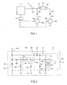
- FIG. 1 shows a schematic representation of an electronic ballast 1.
- the electronic ballast 1 is electrically connected to an electric lamp, which is formed in the embodiment shown as a fluorescent lamp 2.
- the electronic ballast 1 has a half-bridge inverter 11, which is electrically connected to an output with an inductance 12.
- the inductor 12 is further electrically connected to a first lamp filament 21 of the fluorescent lamp 2.
- the inductor 12 also has an electrical connection to a capacitor, which in the exemplary embodiment as a starting capacitor 13a is formed on.
- the ignition capacitor 13a may also be formed as an element of a voltage divider circuit for lamp voltage measurement, which may also be implemented as a resistor divider circuit.
- the electronic ballast 1 comprises a circuit arrangement 14a according to the invention for detecting a crest factor of a lamp burning voltage, which is electrically connected to a first input 141 to the first lamp filament 21 via the ignition capacitor 13a.
- a signal characterizing the lamp burning voltage is transmitted.
- a further capacitor which in the exemplary embodiment is designed as a half-bridge capacitor 13b, is connected to a second lamp filament 22.
- the half-bridge capacitor 13b has an electrical connection to ground potential. It should be noted that in the first embodiment, a circuit 14b is not present.
- the circuit arrangement 14a has a first output 142, which is electrically connected to a control unit 19.
- the circuit 14a is electrically connected to a second output at ground potential.
- the control unit 19 is also electrically connected to an output to an input of the half-bridge inverter 11.
- the circuit arrangement 14a according to the invention is thus designed to detect the crest factor of the lamp firing voltage.
- the second exemplary embodiment of the electronic ballast 1 according to the invention which is likewise shown in FIG. 1, will be explained in more detail below.
- the circuit arrangement 14a is not formed.
- the ignition capacitor 13a is guided to ground potential.
- the circuit arrangement 14b for detecting the crest factor of the lamp current is formed in the second exemplary embodiment.
- the circuit arrangement 14b is electrically connected with a first input 143 to the half-bridge capacitor 13b.
- the circuit arrangement 14b also has a first output 144 in the second exemplary embodiment, which is electrically connected to the control unit 19, wherein a second output of the circuit arrangement 14b is at ground potential.
- an electronic ballast 1 according to the invention either according to the first embodiment or realized according to the second embodiment.
- a realization in which both the signal paths from the inductance 12 via the ignition capacitor 13a via the circuit arrangement 14a to the control unit 19 and additionally the signal path from the second lamp coil 22 via the half-bridge capacitor 13b via the circuit arrangement 14b to the control unit 19 is realized is not provided ,
- FIG. 2 shows a detailed illustration of a circuit arrangement 14a or 14b according to the invention for detecting a crest factor of a lamp burning voltage or a lamp current.
- the circuit arrangement 14b for detecting the crest factor of the lamp current is considered in more detail below.
- the circuit arrangement 14b according to the invention has a first subcircuit 15, which is designed to determine an averaged value of the lamp current from an input signal applied to the circuit arrangement 14b via the input terminal 143.
- the first subcircuit 15 is formed in the embodiment as a low-pass circuit and has a resistor 151 and a capacitor 152.
- the resistor 151 is electrically connected at a first end to an input 15b of the first subcircuit 15 and at a second end to a circuit node of the first subcircuit 15.
- the capacitor 152 is also connected to the circuit node of the first subcircuit 15 and also has a second electrical connection to ground potential.
- the circuit arrangement 14b comprises a second subcircuit 16, which in the exemplary embodiment is designed to determine a maximum permissible value of the lamp current from the input signal applied to the circuit arrangement 14b.
- the second subcircuit 16 has an input 16b, which is electrically connected to the input terminal 143 of the circuit arrangement 14b.
- the second subcircuit 16 has a diode 161 and a capacitor 162.
- the diode 161 is connected with its anode to the input 16b of the second sub-circuit 16. With its cathode, the diode 161 is electrically connected to a first circuit node of the second sub-circuit 16.
- the second subcircuit 16 moreover has two resistors 163, 164 which are used for scaling the signal and for specifying a time constant for this signal, which is the maximum permissible value Crest factor characterized, is formed.
- the resistor 164 is connected to ground potential and connected to a second circuit node of the second subcircuit 16.
- the first resistor 163 is connected between the two circuit nodes of the second subcircuit 16.
- the first subcircuit 15 is connected to an output 15a to a first input 17a of a comparator circuit 17.
- An output 16a of the second subcircuit 16 is electrically connected to a second input 17b of this comparator circuit 17.
- the comparator circuit 17 is formed in the embodiment as a comparator.
- the circuit arrangement 14b in the illustrated embodiment comprises a third subcircuit 18, which is designed for processing and rectifying the input signal which is present at the input 143.
- the third subcircuit comprises a first diode 181 and a second diode 182.
- the first diode 181 is guided with its anode to ground potential, wherein it is connected with its cathode to a first circuit node of the third subcircuit.
- the second diode 182 is guided with its anode at the first circuit node and with its cathode to a second circuit node of the third subcircuit 18.
- the third subcircuit 18 also detects a resistor 183, which is electrically connected to the second circuit node and to ground potential.
- an output 18a of the third subcircuit 18 is electrically connected to the input 15b of the first subcircuit 15.
- the input signal applied to the input 143 is thus transmitted to the third sub-circuit 18 for conditioning and rectification.
- the rectified by this third sub-circuit 18 and processed input signal is then transmitted to the first sub-circuit 15, in which a signal is generated which characterizes the averaged value of the lamp current.
- the input signal applied to the input 143 is transmitted to the second subcircuit 16, in which a maximum permissible value is determined and in which an output signal is generated which characterizes the maximum permissible crest factor.
- the comparison signal generated by the comparator of the comparator circuit 17 is provided as an output signal of the circuit arrangement 14b at the output 144 and transmitted to the control unit 19.
- this control unit 19 is then a scheme with regard to a Setpoint of the crest factor of the lamp current is performed and transmit a corresponding signal to the half-bridge inverter 11.
- the subcircuits 15, 16 and 18 and / or the comparator circuit 17 are designed as digital circuits, thereby enabling digital detection of the processes respectively performed in the subcircuits.
- the sub-circuits 15, 16 and 18 and the comparator circuit 17 are implemented in a microprocessor and the entire detection of the crest factor, as carried out in the circuit 14b, takes place in a digital manner. This means that averaging, peak detection, scaling, timing, and threshold comparison are performed on a digital basis.
- the circuit arrangement 14a is analogous to the circuit arrangement 14b.
Landscapes
- Circuit Arrangements For Discharge Lamps (AREA)
- Measurement Of Current Or Voltage (AREA)
Abstract
Description
Die Erfindung betrifft eine Schaltungsanordnung zur Erfassung eines Crestfaktors eines Lampenstroms oder einer Lampenbrennspannung einer elektrischen Lampe. Des Weiteren betrifft die Erfindung ein Verfahren zum Erfassen eines derartigen Crestfaktors. Darüber hinaus betrifft die Erfindung auch ein elektrisches Vorschaltgerät mit einer Schaltungsanordnung zum Erfassen eines oben genannten Crestfaktors sowie ein Verfahren zum Betreiben einer elektrischen Lampe mit einem elektronischen Vorschaltgerät, bei dem ein Crestfaktor gemäß dem oben genannten Verfahren erfasst wird.The invention relates to a circuit arrangement for detecting a crest factor of a lamp current or a lamp burning voltage of an electric lamp. Furthermore, the invention relates to a method for detecting such a crest factor. Moreover, the invention also relates to an electric ballast having a circuit arrangement for detecting a crest factor mentioned above and a method for operating an electric lamp with an electronic ballast, in which a crest factor is detected according to the above-mentioned method.
Beim Dimmen von elektrischen Lampen, insbesondere Leuchtstofflampen mit elektronischen Vorschaltgeräten, kann sich typischerweise im unteren Bereich des Dimmbereichs, insbesondere im unteren Drittel des Dimmbereichs, eine Schwingung ausbilden, die sich durch das Zusammenspiel von Lampenkennlinie, Resonanzkreis und Regelung ergibt. Dieser Bereich, welcher auch als "Frequenzumkehr"-Bereich bezeichnet wird, tritt besonders stark während einer Hochlaufphase von Amalgam-Lampen auf. Unter extremen Umgebungstemperaturen wird ein derartiger "Frequenzumkehr"-Bereich auch bei Quecksilber-Lampen beobachtet. Diese Schwingung bewirkt eine starke Modulation des Lampenstroms mit Frequenzen von 30 Hz bis 10 kHz und ist zumeist nicht als optische Instabilität erkennbar. Der dadurch verursachte hohe Crestfaktor des Lampenstroms kann jedoch für die elektrische Lampe eine starke Schädigung sowie eine lebensdauerverkürzende Auswirkung haben.When dimming electrical lamps, in particular fluorescent lamps with electronic ballasts, an oscillation can typically develop in the lower area of the dimming area, in particular in the lower third of the dimming area, which results from the interplay of the lamp characteristic curve, resonant circuit and regulation. This area, which is also referred to as the "frequency inversion" area, is particularly noticeable during a startup phase of amalgam lamps. Under extreme ambient temperatures, such a "frequency reversal" range is also observed with mercury lamps. This oscillation causes a strong modulation of the lamp current with frequencies of 30 Hz to 10 kHz and is usually not recognizable as optical instability. However, the high crest factor of the lamp current caused thereby can cause severe damage to the electric lamp as well as a life-shortening effect.
Um den Betrieb mit hohem Lampenstromcrestfaktor zu vermeiden wird versucht, den Bereich der "Frequenzumkehr" durch geeignete Auswahl von Resonanzkreis und Regelung klein zu halten und die schädigende Wirkung des hohen Crestfaktors durch erhöhte Lampenwendelheizung zu verringern. Des Weiteren wird entweder der Bereich der zulässigen Umgebungstemperatur für den Dimmbetrieb eingeschränkt oder der zulässige Dimmbereich bei extremen Umgebungstemperaturen reduziert. Darüber hinaus ist es auch bekannt, dass bei einigen Betriebsgeräten, insbesondere elektronischen Vorschaltgeräten, für Amalgam-Lampen die volle Dimm-Funktion erst nach einer vorgegebenen Zeitdauer nach dem Einschalten freigegeben wird, um dadurch die Hochlaufphase zu überbrücken.In order to avoid high lamp current crest factor operation, it is attempted to minimize the range of "frequency inversion" by appropriate selection of resonant circuit and control and to reduce the damaging effect of the high crest factor by increasing lamp filament heating. Furthermore, either the range of permissible Ambient temperature restricted for dimming operation or the permissible dimming range reduced under extreme ambient temperatures. In addition, it is also known that in some operating devices, in particular electronic ballasts, for amalgam lamps, the full dimming function is released only after a predetermined period of time after switching on, thereby bridging the startup phase.
Der vorliegenden Erfindung liegt deshalb die Aufgabe zugrunde, eine Schaltungsanordnung zum Erfassen eines Crestfaktors eines Lampenstroms oder einer Lampenbrennspannung einer elektrischen Lampe sowie ein Verfahren zum Erfassen eines derartigen Crestfaktors zu schaffen, durch welche bzw. durch welches verhindert werden kann, dass eine elektrische Lampe mit hohem Crestfaktor betrieben wird. Des Weiteren ist es Aufgabe der Erfindung, ein elektronisches Vorschaltgerät zu schaffen, welches eine Schaltungsanordnung zum Erfassen eines Crestfaktors einer elektrischen Lampe aufweist, sowie ein Verfahren zum Betreiben einer elektrischen Lampe mit einem elektronischen Vorschaltgerät zu schaffen, mit dem der schädigende Einfluss eines zu hohen Crestfaktors auf eine elektrische Lampe verhindert werden kann und ein zuverlässiger und sicherer Betrieb der elektrischen Lampe ermöglicht werden kann.The present invention is therefore based on the object to provide a circuit arrangement for detecting a crest factor of a lamp current or a lamp burning voltage of an electric lamp and a method for detecting such a crest factor, by which or can be prevented that a high-powered electric lamp Crest factor is operated. Furthermore, it is an object of the invention to provide an electronic ballast having a circuit arrangement for detecting a crest factor of an electric lamp, and to provide a method for operating an electric lamp with an electronic ballast, with the damaging influence of too high a crest factor can be prevented to an electric lamp and a reliable and safe operation of the electric lamp can be made possible.
Diese Aufgabe wird durch eine Schaltungsanordnung zum Erfassen eines Crestfaktors eines Lampenstroms oder einer Lampenbrennspannung einer elektrischen Lampe, welche die Merkmale nach Patentanspruch 1 aufweist und ein Verfahren zum Erfassen eines derartigen Crestfaktors, welches die Merkmale nach Patentanspruch 16 aufweist, gelöst. Darüber hinaus wird diese Aufgabe auch durch ein elektronisches Vorschaltgerät, welches die Merkmale nach Patentanspruch 12 aufweist, sowie ein Verfahren zum Betreiben einer elektrischen Lampe, welches die Merkmale nach Patentanspruch 18 aufweist, gelöst.This object is achieved by a circuit arrangement for detecting a crest factor of a lamp current or a lamp voltage of an electric lamp, which has the features of claim 1 and a method for detecting such a crest factor, which has the features of
Eine erfindungsgemäße Schaltungsanordnung zum Erfassen eines Crestfaktors einer elektrischen Lampe ist sowohl zum Erfassen eines Lampenstromcrestfaktors als auch eines Lampenbrennspannungscrestfaktors ausgebildet. Die Schaltungsanordnung weist eine erste Teilschaltung auf, wobei diese erste Teilschaltung zum Bestimmen eines gemittelten Werts aus einem an die Schaltungsanordnung angelegten Eingangssignal ausgebildet ist. Des Weiteren umfasst die Schaltungsanordnung eine zweite Teilschaltung, welche zum Bestimmen eines maximalen Werts aus dem an die Schaltungsanordnung angelegten Eingangssignal ausgebildet ist. Als weiteres wesentliches Merkmal weist die Schaltungsanordnung eine Vergleicherschaltung auf, wobei die Vergleicherschaltung zum Erzeugen eines Ausgangssignals in Form eines Vergleichssignals ausgebildet ist. Das durch die Vergleicherschaltung erzeugbare Vergleichsignal ist dabei aus dem den gemittelten Wert charakterisierenden Ausgangssignal der ersten Teilschaltung und einem den maximal zulässigen Crestfaktor charakterisierenden Ausgangssignal der zweiten Teilschaltung erzeugbar. Das Ausgangssignal der zweiten Teilschaltung ist unter Berücksichtigung des den maximalen Wert des Eingangssignals charakterisierenden Signals erzeugbar. Die erfindungsgemäße Schaltungsanordnung ist somit derart konzipiert, dass der Betrieb einer elektrischen Lampe mit hohem Crestfaktor, insbesondere hohem Lampenstromcrestfaktor oder hohem Lampenbrennspannungscrestfaktor, verhindert werden kann. Dadurch kann auch erreicht werden, dass schädigende und lebensdauerverkürzende Beeinträchtigungen der elektrischen Lampe verhindert werden können. Durch die Schaltungsanordnung gemäß der Erfindung kann eine störende Beeinflussung des Einstellens und Betreibens einer elektrischen Lampe durch einen "Frequenzumkehr"-Bereich vermieden werden.A circuit arrangement according to the invention for detecting a crest factor of an electric lamp is designed both for detecting a lamp current crest factor and a lamp burn voltage crest factor. The circuit arrangement has a first subcircuit, wherein this first subcircuit is designed to determine an averaged value from an input signal applied to the circuit arrangement. Furthermore, the circuit arrangement comprises a second subcircuit which is designed to determine a maximum value from the input signal applied to the circuit arrangement is. As a further essential feature, the circuit arrangement has a comparator circuit, wherein the comparator circuit is designed to generate an output signal in the form of a comparison signal. The comparator signal which can be generated by the comparator circuit can be generated from the output signal of the first subcircuit which characterizes the averaged value and an output signal of the second subcircuit which characterizes the maximum permissible crest factor. The output signal of the second subcircuit can be generated taking into account the signal characterizing the maximum value of the input signal. The circuit arrangement according to the invention is thus designed in such a way that the operation of an electric lamp with a high crest factor, in particular a high lamp current crest factor or a high lamp burn voltage crest factor, can be prevented. As a result, it can also be achieved that damaging and life-shortening impairments of the electric lamp can be prevented. By the circuit arrangement according to the invention, a disturbing influence on the setting and operation of an electric lamp by a "frequency reversal" area can be avoided.
In vorteilhafter Weise ist die erste Teilschaltung als Tiefpassschaltung ausgebildet. Die Tiefpassschaltung umfasst dabei in bevorzugter Ausführung einen Widerstand und einen Kondensator, welche mit einem ersten Schaltungsknoten der ersten Teilschaltung elektrisch verbunden sind. Darüber hinaus kann in bevorzugter Ausführung der Kondensator mit einem zweiten elektrischen Anschluss mit Massepotential verbunden sein.Advantageously, the first subcircuit is designed as a low-pass circuit. The low-pass circuit comprises in a preferred embodiment, a resistor and a capacitor, which are electrically connected to a first circuit node of the first sub-circuit. In addition, in a preferred embodiment, the capacitor may be connected to a second electrical connection to ground potential.
Bevorzugt ist ein Ausgang der ersten Teilschaltung mit einem ersten Eingang der Vergleicherschaltung und ein Ausgang der zweiten Teilschaltung mit einem zweiten Eingang der Vergleicherschaltung elektrisch verbunden. Die Ausgangssignale der ersten und der zweiten Teilschaltung werden somit an verschiedenen Eingängen der Vergleicherschaltung, welche in vorteilhafter Weise als Komparator ausgebildet ist, angelegt.Preferably, an output of the first subcircuit is electrically connected to a first input of the comparator circuit and an output of the second subcircuit is electrically connected to a second input of the comparator circuit. The output signals of the first and the second subcircuit are thus applied to different inputs of the comparator circuit, which is advantageously designed as a comparator.
Die zweite Teilschaltung ist in vorteilhafter Weise mit einem ersten Eingangsanschluss der Schaltungsanordnung elektrisch verbunden und umfasst in bevorzugter Ausführung eine Diode und einen Kondensator, welche mit einem ersten Schaltungsknoten der zweiten Teilschaltung elektrisch verbunden sind.The second subcircuit is advantageously electrically connected to a first input terminal of the circuit arrangement and in a preferred embodiment comprises a diode and a capacitor, which are electrically connected to a first circuit node of the second subcircuit.
Die zweite Teilschaltung ist in bevorzugter Weise zum Skalieren des Signals, welches den maximal zulässigen Crestfaktor charakterisiert, und zur Vorgabe einer Zeitkonstante für dieses Signal, welches diesen maximal zulässigen Crestfaktor charakterisiert, ausgebildet. Dazu kann in vorteilhafter Weise vorgesehen sein, dass die zweite Teilschaltung zwei Widerstände aufweist. Dadurch kann ermöglicht werden, dass über die Einstellung der Zeitkonstante in variabler und flexibler Weise auch für eine relativ lange Zeitdauer das den Spitzenwert des Crestfaktors bzw. den maximal zulässigen Crestfaktor charakterisierende Signal erzeugbar und insbesondere am zweiten Eingang der Vergleicherschaltung für eine relativ lange Zeitdauer bereitstellbar ist.The second subcircuit is preferably designed for scaling the signal which characterizes the maximum permissible crest factor and for specifying a time constant for this signal which characterizes this maximum permissible crest factor. For this purpose, it may be provided in an advantageous manner that the second subcircuit has two resistors. It can thus be made possible that the signal which characterizes the peak value of the crest factor or the maximum permissible crest factor can be generated and, in particular, provided at the second input of the comparator circuit for a relatively long period of time by adjusting the time constant in a variable and flexible manner for a relatively long period of time ,
Eine dritte Teilschaltung kann in bevorzugter Weise vorgesehen sein, wobei diese dritte Teilschaltung zur Aufbereitung und Gleichrichtung des Eingangssignals, welches an der Schaltungsanordnung angelegt ist, ausgebildet ist. Durch eine derartige Signalaufbereitung und Gleichrichtung kann die Erfassung des Crestfaktors wesentlich verbessert und exakter durchgeführt werden.A third subcircuit may be provided in a preferred manner, this third subcircuit being designed for processing and rectification of the input signal which is applied to the circuit arrangement. By such a signal conditioning and rectification, the detection of the crest factor can be significantly improved and performed more accurately.
Die dritte Teilschaltung weist einen Ausgang auf, welcher in vorteilhafter Weise mit einem Eingang der ersten Teilschaltung elektrisch verbunden ist. Die dritte Teilschaltung umfasst in bevorzugter Weise zumindest zwei Dioden und einen Widerstand. Dadurch kann die dritte Teilschaltung relativ einfach und aufwandsarm ausgeführt sein und ein für das weitere Verarbeiten sehr gut aufbereitetes und gleichgerichtetes Eingangssignal bereitgestellt werden. In bevorzugter Weise ist der Crestfaktor des Lampenstroms oder der Lampenbrennspannung der elektrischen Lampe zumindest teilweise digital erfassbar. In vorteilhafter Ausführung ist dabei ein Mikroprozessor vorgesehen, in welchem zumindest einer der in den Teilschaltungen und/oder der Vergleicherschaltung durchführbaren Vorgänge digital durchführbar ist.The third subcircuit has an output which is advantageously electrically connected to an input of the first subcircuit. The third subcircuit preferably comprises at least two diodes and a resistor. As a result, the third subcircuit can be designed to be relatively simple and inexpensive, and a very well prepared and rectified input signal can be provided for further processing. Preferably, the crest factor of the lamp current or the lamp burning voltage of the electric lamp is at least partially digitally detectable. In an advantageous embodiment, a microprocessor is provided in which at least one of the operations that can be carried out in the subcircuits and / or the comparator circuit can be carried out digitally.
In bevorzugter Weise ist das Vergleichssignal der Vergleicherschaltung zum Einstellen des Crestfaktors bereitstellbar. Die Schaltungsanordnung ist somit derart ausgebildet, dass das durch die Vergleicherschaltung erzeugte Vergleichsignal als Ausgangssignal der Schaltungsanordnung an weitere Einheiten, die zum Betrieb und zur Einstellung einer elektrischen Lampe bereitgestellt sind, übertragen werden kann und somit eine genaue und sichere Einstellung des Crestfaktors eines Lampenstroms oder einer Lampenbrennspannung durchgeFührt werden kann. Ein sicherer Betrieb der elektrischen Lampe kann dadurch in aufwandsarmer Weise durchgeführt werden.In a preferred manner, the comparison signal of the comparator circuit for setting the crest factor can be provided. The circuit arrangement is thus designed such that the comparison signal generated by the comparator circuit can be transmitted as an output signal of the circuit arrangement to further units that are provided for the operation and adjustment of an electric lamp, and thus an accurate and secure setting of the crest factor of a lamp current or a Lamp burning voltage can be carried out. A safe operation of the electric lamp can be carried out in a low-cost manner.
Ein weiterer Aspekt der Erfindung betrifft ein elektronisches Vorschaltgerät für eine elektrische Lampe, welche eine erfindungsgemäße Schaltungsanordnung oder eine vorteilhafte Ausführung der erfindungsgemäßen Schaltungsanordnung aufweist. Dadurch kann erreicht werden, dass das Betreiben und Einstellen von als Leuchtstofflampen ausgebildeten elektrischen Lampen, welche mit elektronischen Vorschaltgeräten elektrisch verbunden sind, sicher durchgeführt werden kann. Insbesondere beim Dimmen dieser Leuchtstofflampen kann somit ein schädigender oder lebensdauerverkürzender Einfluss durch einen "Frequenzumkehr"-Bereich verhindert werden, da das Auftreten von hohen Crestfaktoren des Lampenstroms oder der Lampenbrennspannung vermieden werden kann.Another aspect of the invention relates to an electronic ballast for an electric lamp, which has a circuit arrangement according to the invention or an advantageous embodiment of the circuit arrangement according to the invention. It can thereby be achieved that the operation and setting of fluorescent lamps designed as electric lamps, which are electrically connected to electronic ballasts, can be performed safely. In particular, when dimming these fluorescent lamps thus a damaging or Lebensdauerverkürzender influence can be prevented by a "frequency reversal" area, since the occurrence of high crest factors of the lamp current or the lamp burning voltage can be avoided.
In bevorzugter Weise ist die in dem elektronischen Vorschaltgerät angeordnete Schaltungsanordnung mit einem ersten Anschluss mit einer ersten Lampenwendel elektrisch verbunden. Darüber hinaus ist die Schaltungsanordnung mit diesem Eingang auch mit einem Halbrückenwechselrichter elektrisch verbunden. Die elektrische Verschaltung der Schaltungsanordnung in dem elektronischen Vorschaltgerät ist dabei derart, dass ein Crestfaktor in einfacher und zuverlässiger Weise genau erfasst werden kann.In a preferred manner, the circuit arrangement arranged in the electronic ballast is electrically connected to a first terminal with a first lamp filament. In addition, the circuit arrangement with this input is also electrically connected to a half-bridge inverter. The electrical connection of the circuit arrangement in the electronic ballast is such that a crest factor can be accurately detected in a simple and reliable manner.
Die Schaltungsanordnung in dem elektronischen Vorschaltgerät weist in bevorzugter Weise einen Ausgang auf, welcher mit einer Regelungseinheit des elektronischen Vorschaltgeräts elektrisch verbunden ist. Das Vergleichssignal, welches als Ausgangssignal von der Schaltungsanordnung bereitgestellt wird, kann somit zum weiteren Verarbeiten und Auswerten direkt an diese Regelungseinheit übertragen werden und zum Einstellen der Lampenparameter und somit auch des Crestfaktors der elektrischen Lampe bereitgestellt werden.The circuit arrangement in the electronic ballast preferably has an output which is electrically connected to a control unit of the electronic ballast. The comparison signal, which is provided as an output signal from the circuit arrangement, can thus be transmitted directly to this control unit for further processing and evaluation and can be provided for setting the lamp parameters and thus also the crest factor of the electric lamp.
Es kann vorgesehen sein, dass das elektronische Vorschaltgerät zum Einstellen und Betreiben mit einer Leuchtstofflampe, insbesondere einer Amalgam-Lampe oder einer Quecksilber-Lampe, elektrisch verbunden ist. Gerade bei diesen Lampen kann somit ein sicherer Betrieb ohne einen zu hohen Crestfaktor des Lampenstroms oder der Lampenbrennspannung durchgeführt werden.It can be provided that the electronic ballast for setting and operation with a fluorescent lamp, in particular an amalgam lamp or a mercury lamp, is electrically connected. Especially with these lamps safe operation can thus be performed without too high a crest factor of the lamp current or the lamp burning voltage.
Bei einem erfindungsgemäßen Verfahren zum Erfassen eines Crestfaktors einer Lampenbrennspannung oder eines Lampenstroms einer elektrischen Lampe durch eine Schaltungsanordnung wird in einem ersten Verfahrensschritt mittels einer ersten Teilschaltung ein gemittelter Wert aus einem an die Schaltungsanordnung angelegten Eingangssignal bestimmt. Des Weiteren wird ein maximaler Wert aus diesem an die Schaltungsanordnung angelegten Eingangssignal mittels einer zweiten Teilschaltung bestimmt. Aus dem den maximalen Wert charakterisierenden Signal wird mittels der zweiten Teilschaltung ein den maximal zulässigen Crestfaktor charakterisierendes Ausgangssignal bestimmt bzw. erzeugt. Aus dem Ausgangssignal der ersten Teilschaltung, welches den gemittelten Wert charakterisiert und einem Ausgangssignal der zweiten Teilschaltung, welches den maximal zulässigen Crestfaktor charakterisiert, wird in einem weiteren Verfahrensschritt ein Vergleichen dieser beiden Signale durchgeführt. Das durch den Vergleich erzeugte Vergleichssignal wird als Ausgangssignal der Schaltungsanordnung bereitgestellt. Durch das erfindungsgemäße Verfahren kann eine einfache und aufwandsarme sowie exakte Erfassung eines Crestfaktors des Lampenstroms oder der Lampenbrennspannung durchgeführt werden. Das bei dem erfindungsgemäßen Verfahren erzeugte Vergleichssignal kann dann als Informationssignal zur weiteren Einstellung und Regelung von Lampenparametem herangezogen werden, derart, dass der Betrieb einer elektrischen Lampe mit einem zu hohen Crestfaktor des Lampenstroms oder der Lampenbrennspannung verhindert werden kann.In a method according to the invention for detecting a crest factor of a lamp burning voltage or a lamp current of an electric lamp by means of a circuit arrangement, in a first method step an averaged value is determined from an input signal applied to the circuit arrangement by means of a first subcircuit. Furthermore, a maximum value from this input signal applied to the circuit arrangement is determined by means of a second subcircuit. Out of that the maximum value Characterizing signal is determined by the second subcircuit, a maximum allowable Crestfaktor characterizing output signal or generated. From the output signal of the first subcircuit, which characterizes the averaged value and an output signal of the second subcircuit, which characterizes the maximum permissible crest factor, a comparison of these two signals is carried out in a further method step. The comparison signal generated by the comparison is provided as an output signal of the circuit arrangement. By the method according to the invention, a simple and low-effort and exact detection of a crest factor of the lamp current or the lamp burning voltage can be carried out. The comparison signal generated in the method according to the invention can then be used as an information signal for further adjustment and control of Lampenparametem such that the operation of an electric lamp with a high crest factor of the lamp current or the lamp burning voltage can be prevented.
In vorteilhafter Weise wird das Eingangssignal vor dem Bestimmen des gemittelten Werts aufbereitet und gleichgerichtet.Advantageously, the input signal is conditioned and rectified prior to determining the averaged value.
Ein weiterer Aspekt der Erfindung betrifft ein Verfahren zum Betreiben einer elektrischen Lampe, welche mit einem elektronischen Vorschaltgerät elektrisch verbunden ist, wobei bei diesem erfindungsgemäßen Verfahren zum Betreiben der elektrischen Lampe ein Crestfaktor einer Lampenbrennspannung oder eines Lampenstroms nach einem oben erläuterten erfindungsgemäßen Verfahren zum Erfassen eines derartigen Crestfaktors erfasst wird. Dadurch kann erreicht werden, dass das Betreiben und Einstellen der elektrischen Lampe sicher und zuverlässig durchgeführt werden kann.Another aspect of the invention relates to a method for operating an electric lamp, which is electrically connected to an electronic ballast, wherein in this inventive method for operating the electric lamp, a crest factor of a lamp voltage or a lamp current according to a method of the invention described above for detecting such Crest Factors is detected. It can thereby be achieved that the operation and adjustment of the electric lamp can be performed safely and reliably.
Weitere Ausgestaltungen der Erfindung sind in den Unteransprüchen angegeben.Further embodiments of the invention are specified in the subclaims.
Vorteilhafte Ausgestaltungen der erfindungsgemäßen Schaltungsanordnung sowie dem erfindungsgemäßen elektronischen Vorschaltgerät sind, soweit übertragbar, auch als erfindungsgemäße Ausgestaltungen des erfindungsgemäßen Verfahrens zum Erfassen eines Crestfaktors einer Lampenbrennspannung oder eines Lampenstroms einer elektrischen Lampe, sowie dem erfindungsgemäßen Verfahren zum Betreiben einer elektrischen Lampe anzusehen.Advantageous embodiments of the circuit arrangement according to the invention and the electronic ballast according to the invention are, insofar as transferable, as inventive embodiments of the invention for detecting a crest factor of a lamp voltage or a lamp current of an electric lamp, as well as the inventive method for operating an electric lamp.
Bei der Erfindung wird somit ein Crestfaktor des Lampenstroms oder der Lampenbrennspannung mit einer geeigneten Schaltungsanordnung, welche in bevorzugter Weise in einem elektronischen Vorschaltgerät angeordnet ist, anhand einer Messung des Lampenstroms oder der Lampenbrennspannung ermittelt. Der ermittelte Crestfaktor wird mit einem zulässigen Maximalwert verglichen, wobei bei Überschreitung des Maximalwerts durch den ermittelten Wert des Crestfaktors eine Leistung der elektrischen Lampe soweit angehoben werden kann, bis der zulässige Maximalwert wieder unterschritten ist. Mit der Erfindung kann auch erreicht werden, dass in kritischen Phasen des Betriebs, insbesondere während des Hochlaufens der elektrischen Lampe, der Dimmbereich quasi nach unten hin nur soweit erforderlich bzw. nur minimal eingeschränkt wird.In the invention, therefore, a crest factor of the lamp current or the lamp burning voltage with a suitable circuit arrangement, which in a preferred manner in a arranged electronic ballast, determined based on a measurement of the lamp current or the lamp burning voltage. The determined crest factor is compared with a permissible maximum value, wherein when the maximum value is exceeded by the determined value of the crest factor, a power of the electric lamp can be increased until the permissible maximum value is fallen below again. With the invention it can also be achieved that in critical phases of the operation, in particular during the run-up of the electric lamp, the dimming range is virtually restricted as far as necessary or only minimally downwards.
Ausführungsbeispiele der Erfindung werden nachfolgend anhand schematischer Zeichnungen näher erläutert. Es zeigen:
- Figur 1
- ein erstes und zweites Ausführungsbeispiel eines erfindungsgemäßen elektronischen Vorschaltgeräts, welches mit einer elektrischen Lampe verbunden ist; und
Figur 2- eine Darstellung einer erfindungsgemäßen Schaltungsanordnung zum Erfassen eines Crestfaktors eines Lampenstroms oder einer Lampenbrennspannung.
- FIG. 1
- a first and second embodiment of an electronic ballast according to the invention, which is connected to an electric lamp; and
- FIG. 2
- an illustration of a circuit arrangement according to the invention for detecting a crest factor of a lamp current or a lamp burning voltage.
In den Figuren 1 und 2 werden gleiche oder funktionsgleiche Elemente mit den gleichen Bezugszeichen versehen.In FIGS. 1 and 2, identical or functionally identical elements are given the same reference numerals.
In Figur 1 ist eine schematische Darstellung eines elektronischen Vorschaltgeräts 1 gezeigt. Das elektronische Vorschaltgerät 1 ist mit einer elektrischen Lampe, welche im gezeigten Ausführungsbeispiel als Leuchtstofflampe 2 ausgebildet ist, elektrisch verbunden.FIG. 1 shows a schematic representation of an electronic ballast 1. The electronic ballast 1 is electrically connected to an electric lamp, which is formed in the embodiment shown as a
In der in Figur 1 gezeigten Darstellung sind zwei verschiedene Ausführungsbeispiele der Erfindung gezeigt. Nachfolgend wird zunächst die Realisierung des ersten Ausführungsbeispiels näher erläutert. Das elektronische Vorschaltgerät 1 weist einen Halbbrückenwechselrichter 11 auf, welcher mit einem Ausgang mit einer Induktivität 12 elektrisch verbunden ist. Die Induktivität 12 ist des Weiteren mit einer ersten Lampenwendel 21 der Leuchtstofflampe 2 elektrisch verbunden. Darüber hinaus weist die Induktivität 12 auch eine elektrische Verbindung zu einem Kondensator, welcher im Ausführungsbeispiel als Zündkondensator 13a ausgebildet ist, auf. Anzumerken ist, dass der Zündkondensator 13a auch als Element einer Spannungsteilerschaltung zur Lampenspannungsmessung ausgebildet sein kann, welche auch als Widerstandsteilerschaltung realisiert sein kann. Des Weiteren umfasst das elektronische Vorschaltgerät 1 eine erfindungsgemäße Schaltungsanordnung 14a zum Erfassen eines Crestfaktors einer Lampenbrennspannung, welche mit einem ersten Eingang 141 mit der ersten Lampenwendel 21 über den Zündkondensator 13a elektrisch verbunden ist. Im Signalpfad zwischen der Induktivität 12 und der ersten Lampenwendel 21 sowie im Signalpfad zwischen der Induktivität 12 bis zur Schaltungsanordnung 14a wird ein die Lampenbrennspannung charakterisierendes Signal übertragen. Des Weiteren ist ein weiterer Kondensator, welcher im Ausführungsbeispiel als Halbbrückenkondensator 13b ausgebildet ist, mit einer zweiten Lampenwendel 22 verbunden. Darüber hinaus weist der Halbbrückenkondensator 13b im ersten Ausführungsbeispiel eine elektrische Verbindung zu Massepotential auf. Anzumerken ist, dass im ersten Ausführungsbeispiel eine Schaltungsanordnung 14b nicht vorhanden ist.In the illustration shown in Figure 1, two different embodiments of the invention are shown. The realization of the first exemplary embodiment will first be explained in more detail below. The electronic ballast 1 has a half-
Wie des Weiteren aus der Darstellung in Figur 1 zu entnehmen ist, weist die Schaltungsanordnung 14a einen ersten Ausgang 142 auf, welcher mit einer Regelungseinheit 19 elektrisch verbunden ist. Darüber hinaus ist die Schaltungsanordnung 14a mit einem zweiten Ausgang mit Massepotential elektrisch verbunden. Die Regelungseinheit 19 ist darüber hinaus mit einem Ausgang mit einem Eingang des Halbbrückenwechselrichters 11 elektrisch verbunden. Im oben erläuterten ersten Ausführungsbeispiel ist somit die erfindungsgemäße Schaltungsanordnung 14a zum Erfassen des Crestfaktors der Lampenbrennspannung ausgebildet.As can also be seen from the illustration in FIG. 1, the
Im Nachfolgenden wird das in Figur 1 ebenfalls dargestellte zweite Ausführungsbeispiel des erfindungsgemäßen elektronischen Vorschaltgeräts 1 näher erläutert. Anzumerken ist, dass bei diesem zweiten Ausführungsbeispiel die Schaltungsanordnung 14a nicht ausgebildet ist. In diesem zweiten Ausführungsbeispiel ist der Zündkondensator 13a an Massepotential geführt. Anstatt der Schaltungsanordnung 14a ist im zweiten Ausführungsbeispiel die Schaltungsanordnung 14b zum Erfassen des Crestfaktors des Lampenstroms ausgebildet. Die Schaltungsanordnung 14b ist mit einem ersten Eingang 143 mit dem Halbbrückenkondensator 13b elektrisch verbunden. Entsprechend dem ersten Ausführungsbeispiel weist auch im zweiten Ausführungsbeispiel die Schaltungsanordnung 14b einen ersten Ausgang 144 auf, welcher mit der Regelungseinheit 19 elektrisch verbunden ist, wobei ein zweiter Ausgang der Schaltungsanordnung 14b an Massepotential liegt. Es sei erwähnt, dass ein erfindungsgemäßes elektronisches Vorschaltgerät 1 entweder gemäß dem ersten Ausführungsbeispiel oder gemäß dem zweiten Ausführungsbeispiel realisiert ist. Eine Realisierung, bei der sowohl die Signalpfade von der Induktivität 12 über den Zündkondensator 13a über die Schaltungsanordnung 14a hin zur Regelungseinheit 19 und zusätzlich der Signalpfad von der zweiten Lampenwendel 22 über den Halbbrückenkondensator 13b über die Schaltungsordnung 14b zur Regelungseinheit 19 realisiert ist, ist nicht vorgesehen.The second exemplary embodiment of the electronic ballast 1 according to the invention, which is likewise shown in FIG. 1, will be explained in more detail below. It should be noted that in this second embodiment, the
In Figur 2 ist eine detaillierte Darstellung einer erfindungsgemäßen Schaltungsanordnung 14a oder 14b zum Erfassen eines Crestfaktors einer Lampenbrennspannung bzw. eines Lampenstroms gezeigt. Zur näheren Erläuterung wird nachfolgend die Schaltungsanordnung 14b zum Erfassen des Crestfaktors des Lampenstroms näher betrachtet. Wie aus Figur 2 zu erkennen ist, weist die erfindungsgemäße Schaltungsanordnung 14b eine erste Teilschaltung 15 auf, welche zum Bestimmen eines gemittelten Werts des Lampenstroms aus einem an die Schaltungsanordnung 14b über den Eingangsanschluss 143 angelegten Eingangssignal ausgebildet ist. Die erste Teilschaltung 15 ist im Ausführungsbeispiel als Tiefpassschaltung ausgebildet und weist einen Widerstand 151 sowie einen Kondensator 152 auf. Der Widerstand 151 ist mit einem ersten Ende mit einem Eingang 15b der ersten Teilschaltung 15 und mit einem zweiten Ende mit einem Schaltungsknoten der ersten Teilschaltung 15 elektrisch verbunden. Der Kondensator 152 ist ebenfalls mit dem Schaltungsknoten der ersten Teilschaltung 15 verbunden und weist darüber hinaus eine zweite elektrische Verbindung zu Massepotential auf.FIG. 2 shows a detailed illustration of a
Des Weiteren umfasst die Schaltungsanordnung 14b eine zweite Teilschaltung 16, welche im Ausführungsbeispiel zum Bestimmen eines maximal zulässigen Werts des Lampenstroms aus dem an die Schaltungsanordnung 14b angelegten Eingangssignal ausgebildet ist. Wie zu erkennen ist, weist die zweite Teilschaltung 16 einen Eingang 16b auf, welcher mit dem Eingangsanschluss 143 der Schaltungsanordnung 14b elektrisch verbunden ist. Zur Erzeugung eines maximal zulässigen Werts aus dem Eingangssignal weist die zweite Teilschaltung 16 eine Diode 161 sowie einen Kondensator 162 auf. Die Diode 161 ist dabei mit ihrer Anode mit dem Eingang 16b der zweiten Teilschaltung 16 verbunden. Mit ihrer Kathode ist die Diode 161 mit einem ersten Schaltungsknoten der zweiten Teilschaltung 16 elektrisch verbunden. Mit diesem ersten Schaltungsknoten ist auch der Kondensator 162 elektrisch verbunden, wobei dieser Kondensator 162 mit seinem zweiten Ende mit Massepotential elektrisch verbunden ist. Im gezeigten Ausführungsbeispiel gemäß Figur 2 weist die zweite Teilschaltung 16 darüber hinaus zwei Widerstände 163, 164 auf, welche zur Skalierung des Signals und zur Vorgabe einer Zeitkonstante für dieses Signal, welches den maximal zulässigen Crestfaktor charakterisiert, ausgebildet ist. Wie aus der Darstellung in Figur 2 zu erkennen ist, ist der Widerstand 164 an Massepotential angeschlossen und mit einem zweiten Schaltungsknoten der zweiten Teilschaltung 16 verbunden. Der erste Widerstand 163 ist zwischen die beiden Schaltungsknoten der zweiten Teilschaltung 16 geschaltet. Wie aus der Darstellung in Figur 2 zu erkennen ist, ist die erste Teilschaltung 15 mit einem Ausgang 15a mit einem ersten Eingang 17a einer Vergleicherschaltung 17 verbunden. Ein Ausgang 16a der zweiten Teilschaltung 16 ist mit einem zweiten Eingang 17b dieser Vergleicherschaltung 17 elektrisch verbunden. Die Vergleicherschaltung 17 ist im Ausführungsbeispiel als Komparator ausgebildet.Furthermore, the
Des Weitem umfasst die Schaltungsanordnung 14b im dargestellten Ausführungsbeispiel eine dritte Teilschaltung 18, welche zum Aufbereiten und Gleichrichten des Eingangsignals, welches am Eingang 143 anliegt, ausgebildet ist. Die dritte Teilschaltung umfasst eine erste Diode 181 sowie eine zweite Diode 182. Die erste Diode 181 ist mit ihrer Anode an Massepotential geführt, wobei sie mit ihrer Kathode mit einem ersten Schaltungsknoten der dritten Teilschaltung verbunden ist. Des Weiteren ist die zweite Diode 182 mit ihrer Anode an dem ersten Schaltungsknoten und mit ihrer Kathode an einen zweiten Schaltungsknoten der dritten Teilschaltung 18 geführt. Darüber hinaus erfasst die dritte Teilschaltung 18 auch einen Widerstand 183, welcher mit dem zweiten Schaltungsknoten und mit Massepotential elektrisch verbunden ist. Wie aus der Darstellung in Figur 2 zu erkennen ist, ist ein Ausgang 18a der dritten Teilschaltung 18 mit dem Eingang 15b der ersten Teilschaltung 15 elektrisch verbunden.By far, the
Das an den Eingang 143 angelegte Eingangssignal wird somit an die dritte Teilschaltung 18 zur Aufbereitung und Gleichrichtung übertragen. Das durch diese dritte Teilschaltung 18 gleichgerichtete und aufbereitete Eingangssignal wird dann an die erste Teilschaltung 15 übertragen, in der ein Signal generiert wird, welches den gemittelten Wert des Lampenstroms charakterisiert. In entsprechender Weise wird das am Eingang 143 angelegte Eingangssignal an die zweite Teilschaltung 16 übertragen, in welcher ein maximal zulässiger wert ermittelt wird und in der ein Ausgangssignal erzeugt wird, welches den maximal zulässigen Crestfaktor charakterisiert. In der Vergleicherschaltung 17 wird dann ein Vergleich zwischen den Ausgangssignalen der Teilschaltungen 15 und 16 durchgeführt und das durch den Komparator der Vergleicherschaltung 17 erzeugte Vergleichsignal als Ausgangssignal der Schaltungsanordnung 14b am Ausgang 144 bereitgestellt und an die Regelungseinheit 19 übertragen. In dieser Regelungseinheit 19 wird dann eine Regelung im Hinblick auf einen Sollwert des Crestfaktors des Lampenstroms durchgeführt und ein entsprechendes Signal an den Halbbrückenwechselrichter 11 übertragen. Durch die Erfindung kann der Betrieb der Leuchtstofflampe 2 ohne zu hohen Crestfaktor durchgeführt werden, wobei dadurch ein schädigender oder lebensdauerverkürzender Betrieb der Leuchtstofflampe 2 verhindert werden kann.The input signal applied to the
Es kann auch vorgesehen sein, dass zumindest einige der Teilschaltungen 15, 16 und 18 und/oder die Vergleicherschaltung 17 als digitale Schaltungen ausgebildet sind und dadurch eine digitale Erfassung der jeweils in den Teilschaltungen durchgeführten Vorgänge ermöglicht wird. In besonders vorteilhafter Weise kann vorgesehen sein, dass die Teilschaltungen 15, 16 und 18 sowie die Vergleicherschaltung 17 in einem Mikroprozessor realisiert sind und die gesamte Erfassung des Crestfaktors, wie sie in der Schaltungsanordnung 14b durchgeführt wird, in digitaler Weise erfolgt. Dies bedeutet, dass die Mittelwertbildung, die Spitzenwerterfassung, die Skalierung, das Zeitverhalten und der Schwellwertvergleich auf digitaler Basis durchgeführt wird.It can also be provided that at least some of the
Die Schaltungsanordnung 14a ist analog zur Schaltungsanordnung 14b ausgebildet.The
Claims (19)
dadurch gekennzeichnet, dass
die erste Teilschaltung (15) als Tiefpassschaltung ausgebildet ist.Circuit arrangement according to Claim 1,
characterized in that
the first subcircuit (15) is designed as a low-pass circuit.
dadurch gekennzeichnet, dass
ein Ausgang (15a) der ersten Teilschaltung (15) mit einem ersten Eingang (17a) der Vergleicherschaltung (17) und ein Ausgang (16a) der zweiten Teilschaltung (16) mit einem zweiten Eingang (17b) der Vergleicherschaltung (17) elektrisch verbunden ist.Circuit arrangement according to Claim 1 or 2,
characterized in that
an output (15a) of the first subcircuit (15) is electrically connected to a first input (17a) of the comparator circuit (17) and an output (16a) of the second subcircuit (16) is electrically connected to a second input (17b) of the comparator circuit (17) ,
dadurch gekennzeichnet, dass
die zweite Teilschaltung (16) mit einem Eingang (16b) mit einem ersten Eingangsanschluss (141; 143) der Schaltungsanordnung (14a, 14b) elektrisch verbunden ist, wobei die zweite Teilschaltung (16) eine Diode (161) und einen Kondensator (162) aufweist.Circuit arrangement according to one of the preceding claims,
characterized in that
the second subcircuit (16) having an input (16b) is electrically connected to a first input terminal (141; 143) of the circuit arrangement (14a, 14b), the second subcircuit (16) comprising a diode (161) and a capacitor (162) having.
dadurch gekennzeichnet, dass
die zweite Teilschaltung (16) zum Skalieren des Signals, welches den maximal zulässigen Crestfaktor charakterisiert, und zur Vorgabe einer Zeitkonstante für das Signal, welches den maximal zulässigen Crestfaktor charakterisiert, ausgebildet ist.Circuit arrangement according to one of the preceding claims,
characterized in that
the second sub-circuit (16) for scaling the signal, which characterizes the maximum allowable crest factor, and for setting a time constant for the signal, which characterizes the maximum allowable crest factor is formed.
gekennzeichnet durch
eine dritte Teilschaltung (18), welche zur Aufbereitung und Gleichrichtung des Eingangssignals ausgebildet ist,Circuit arrangement according to one of the preceding claims,
marked by
a third sub-circuit (18), which is designed for processing and rectification of the input signal,
dadurch gekennzeichnet, dass
die dritte Teilschaltung (18) mit einem Ausgang (18a) mit einem Eingang (15b) der ersten Teilschaltung (15) elektrisch verbunden ist.Circuit arrangement according to Claim 6,
characterized in that
the third subcircuit (18) having an output (18a) is electrically connected to an input (15b) of the first subcircuit (15).
dadurch gekennzeichnet, dass
die dritte Teilschaltung (18) zumindest zwei Dioden (181, 182) und einen Widerstand (183) aufweist.Circuit arrangement according to Claim 6 or 7,
characterized in that
the third subcircuit (18) has at least two diodes (181, 182) and a resistor (183).
dadurch gekennzeichnet, dass
der Crestfaktor des Lampenstroms oder der Lampenbrennspannung zumindest teilweise digital erfassbar ist.Circuit arrangement according to one of the preceding claims,
characterized in that
the crest factor of the lamp current or the lamp voltage is at least partially digitally detectable.
gekennzeichnet durch
einen Mikroprozessor, in welchem zumindest einer der in den Teilschaltungen (15, 16, 18) und/oder der Vergleicherschaltung (17) durchführbaren Vorgänge digital durchführbar ist.Circuit arrangement according to Claim 9,
marked by
a microprocessor in which at least one of the in the sub-circuits (15, 16, 18) and / or the comparator circuit (17) feasible operations is digitally feasible.
dadurch gekennzeichnet, dass
das Vergleichssignal der Vergleicherschaltung (17) zum Einstellen des Crestfaktors bereitstellbar ist.Circuit arrangement according to one of the preceding claims,
characterized in that
the comparison signal of the comparator circuit (17) can be provided for setting the crest factor.
dadurch gekennzeichnet, dass
die Schaltungsanordnung (14a; 14b) mit einem Eingang (141; 143) mit einer Lampenwendel (21; 22) elektrisch verbunden ist.Electronic ballast according to claim 12,
characterized in that
the circuit arrangement (14a; 14b) is electrically connected to an input (141; 143) with a lamp filament (21; 22).
dadurch gekennzeichnet, dass
die Schaltungsanordnung (14a; 14b) mit einem ersten Ausgang (142; 144) mit einer Regelungseinheit (19) elektrisch verbunden ist.Electronic ballast according to claim 12 or 13,
characterized in that
the circuit arrangement (14a; 14b) is electrically connected to a first output (142; 144) with a control unit (19).
dadurch gekennzeichnet, dass
das elektronische Vorschaltgerät (1) mit einer Leuchtstofflampe (2), insbesondere einer Amalgam-Lampe oder Quecksilber-Lampe, elektrisch verbunden ist.Electronic ballast according to one of Claims 12 to 14,
characterized in that
the electronic ballast (1) is electrically connected to a fluorescent lamp (2), in particular an amalgam lamp or mercury lamp.
dadurch gekennzeichnet, dass
das Eingangssignal vor dem Bestimmen des gemittelten Crestfaktors aufbereitet und gleichgerichtet wird.Method according to claim 16,
characterized in that
the input signal is conditioned and rectified prior to determining the averaged crest factor.
dadurch gekennzeichnet, dass
das Verfahren nach Anspruch 16 oder 17 in dem elektronischen Vorschaltgerät (1) durchgeführt wird.Method according to claim 18,
characterized in that
the method according to claim 16 or 17 is carried out in the electronic ballast (1).
Applications Claiming Priority (1)
| Application Number | Priority Date | Filing Date | Title |
|---|---|---|---|
| DE102005027012A DE102005027012A1 (en) | 2005-06-10 | 2005-06-10 | Circuit arrangement and method for detecting a crest factor of a lamp current or a lamp burning voltage of an electric lamp |
Publications (2)
| Publication Number | Publication Date |
|---|---|
| EP1732365A2 true EP1732365A2 (en) | 2006-12-13 |
| EP1732365A3 EP1732365A3 (en) | 2007-10-24 |
Family
ID=36992021
Family Applications (1)
| Application Number | Title | Priority Date | Filing Date |
|---|---|---|---|
| EP06011752A Withdrawn EP1732365A3 (en) | 2005-06-10 | 2006-06-07 | Circuit and method for detecting the crest factor of a lamp current or a lamp voltage |
Country Status (5)
| Country | Link |
|---|---|
| US (1) | US7355356B2 (en) |
| EP (1) | EP1732365A3 (en) |
| CN (1) | CN1956617A (en) |
| CA (1) | CA2549808A1 (en) |
| DE (1) | DE102005027012A1 (en) |
Cited By (1)
| Publication number | Priority date | Publication date | Assignee | Title |
|---|---|---|---|---|
| WO2008083855A1 (en) | 2007-01-11 | 2008-07-17 | Osram Gesellschaft mit beschränkter Haftung | Method for determining a crest factor of a lamp current of an electric lamp |
Families Citing this family (2)
| Publication number | Priority date | Publication date | Assignee | Title |
|---|---|---|---|---|
| JP5380138B2 (en) * | 2009-04-06 | 2014-01-08 | 本田技研工業株式会社 | Grid interconnection inverter |
| DE102009023884A1 (en) * | 2009-06-04 | 2011-01-27 | Osram Gesellschaft mit beschränkter Haftung | Electronic ballast and method for operating at least one discharge lamp |
Citations (6)
| Publication number | Priority date | Publication date | Assignee | Title |
|---|---|---|---|---|
| US3502983A (en) * | 1968-11-20 | 1970-03-24 | Bell Telephone Labor Inc | Signal peak-to-average ratio detector |
| US5220276A (en) * | 1991-06-11 | 1993-06-15 | Keithley Corporation | Crest factor measurement device |
| US5363020A (en) * | 1993-02-05 | 1994-11-08 | Systems And Service International, Inc. | Electronic power controller |
| WO2000040058A1 (en) * | 1998-12-29 | 2000-07-06 | Koninklijke Philips Electronics N.V. | Dimmable electronic ballast with single stage feedback inverter |
| WO2002019779A1 (en) * | 2000-08-28 | 2002-03-07 | Koninklijke Philips Electronics N.V. | Circuit device |
| WO2004028206A2 (en) * | 2002-09-19 | 2004-04-01 | International Rectifier Corporation | Adaptive cfl control circuit |
Family Cites Families (2)
| Publication number | Priority date | Publication date | Assignee | Title |
|---|---|---|---|---|
| ATE259574T1 (en) * | 2000-06-15 | 2004-02-15 | Univ City Hong Kong | DIMMABLE ECG |
| JP4244747B2 (en) * | 2002-11-08 | 2009-03-25 | ウシオ電機株式会社 | High pressure discharge lamp lighting device |
-
2005
- 2005-06-10 DE DE102005027012A patent/DE102005027012A1/en not_active Withdrawn
-
2006
- 2006-06-07 EP EP06011752A patent/EP1732365A3/en not_active Withdrawn
- 2006-06-08 CA CA002549808A patent/CA2549808A1/en not_active Abandoned
- 2006-06-09 US US11/449,838 patent/US7355356B2/en active Active
- 2006-06-09 CN CNA200610149512XA patent/CN1956617A/en active Pending
Patent Citations (6)
| Publication number | Priority date | Publication date | Assignee | Title |
|---|---|---|---|---|
| US3502983A (en) * | 1968-11-20 | 1970-03-24 | Bell Telephone Labor Inc | Signal peak-to-average ratio detector |
| US5220276A (en) * | 1991-06-11 | 1993-06-15 | Keithley Corporation | Crest factor measurement device |
| US5363020A (en) * | 1993-02-05 | 1994-11-08 | Systems And Service International, Inc. | Electronic power controller |
| WO2000040058A1 (en) * | 1998-12-29 | 2000-07-06 | Koninklijke Philips Electronics N.V. | Dimmable electronic ballast with single stage feedback inverter |
| WO2002019779A1 (en) * | 2000-08-28 | 2002-03-07 | Koninklijke Philips Electronics N.V. | Circuit device |
| WO2004028206A2 (en) * | 2002-09-19 | 2004-04-01 | International Rectifier Corporation | Adaptive cfl control circuit |
Cited By (1)
| Publication number | Priority date | Publication date | Assignee | Title |
|---|---|---|---|---|
| WO2008083855A1 (en) | 2007-01-11 | 2008-07-17 | Osram Gesellschaft mit beschränkter Haftung | Method for determining a crest factor of a lamp current of an electric lamp |
Also Published As
| Publication number | Publication date |
|---|---|
| US20060279231A1 (en) | 2006-12-14 |
| CN1956617A (en) | 2007-05-02 |
| US7355356B2 (en) | 2008-04-08 |
| DE102005027012A1 (en) | 2006-12-14 |
| CA2549808A1 (en) | 2006-12-10 |
| EP1732365A3 (en) | 2007-10-24 |
Similar Documents
| Publication | Publication Date | Title |
|---|---|---|
| EP0422255B1 (en) | Electronic ballast | |
| EP0876742B1 (en) | Method and control circuit for regulation of the operational characteristics of gas discharge lamps | |
| DE19900153A1 (en) | Integrated gate driver circuit | |
| EP2377372B1 (en) | Method, device and lighting system | |
| DE69911376T2 (en) | METHOD AND ARRANGEMENT FOR OPERATING ELECTRONIC CONTROL GEARS FOR DISCHARGE LAMPS OF HIGH INTENSITY | |
| DE102004039421B4 (en) | Ballast of a discharge lamp and method for driving a discharge lamp | |
| EP2258149B1 (en) | Detection of the type of an hid lamp by a multi-lamp operating device and lighting system | |
| EP1901591B1 (en) | Ignition of gas discharge lamps in variable ambient conditions | |
| EP1732365A2 (en) | Circuit and method for detecting the crest factor of a lamp current or a lamp voltage | |
| DE69709604T2 (en) | CIRCUIT | |
| EP1424881B1 (en) | Method and device for driving a fluorescent lamp | |
| EP1276355B1 (en) | Circuit arrangement to determine the pre-heating power | |
| DE60122192T2 (en) | CIRCUIT | |
| EP2274960B1 (en) | Method and circuit arrangement for operating at least one discharge lamp | |
| EP1992203B1 (en) | Electronic ballast and method for operating an electrical lamp | |
| WO2008128577A1 (en) | Circuit arrangement for igniting and operating a discharge lamp | |
| EP2208401B1 (en) | Electronic ballast and method for operating at least one first and second discharge lamp | |
| DE102020103921B4 (en) | Operating device and method for operating a lighting arrangement | |
| EP3580824B1 (en) | Circuit for limiting the making current in a power supply unit | |
| EP3195698B1 (en) | Electronic ballast and method for controlling a load | |
| DE10127135B4 (en) | Dimmable electronic ballast | |
| DE102005018763A1 (en) | Operating devices with evaluation of the lamp temperature during lamp control | |
| EP2468078B1 (en) | Electronic ballast and method for operating at least one discharge lamp | |
| DE69619252T2 (en) | METHOD AND DEVICE FOR CONTROLLING GAS DISCHARGE LAMPS | |
| EP2119324A1 (en) | Method for determining a crest factor of a lamp current of an electric lamp |
Legal Events
| Date | Code | Title | Description |
|---|---|---|---|
| PUAI | Public reference made under article 153(3) epc to a published international application that has entered the european phase |
Free format text: ORIGINAL CODE: 0009012 |
|
| AK | Designated contracting states |
Kind code of ref document: A2 Designated state(s): AT BE BG CH CY CZ DE DK EE ES FI FR GB GR HU IE IS IT LI LT LU LV MC NL PL PT RO SE SI SK TR |
|
| AX | Request for extension of the european patent |
Extension state: AL BA HR MK YU |
|
| PUAL | Search report despatched |
Free format text: ORIGINAL CODE: 0009013 |
|
| AK | Designated contracting states |
Kind code of ref document: A3 Designated state(s): AT BE BG CH CY CZ DE DK EE ES FI FR GB GR HU IE IS IT LI LT LU LV MC NL PL PT RO SE SI SK TR |
|
| AX | Request for extension of the european patent |
Extension state: AL BA HR MK YU |
|
| AKX | Designation fees paid | ||
| STAA | Information on the status of an ep patent application or granted ep patent |
Free format text: STATUS: THE APPLICATION IS DEEMED TO BE WITHDRAWN |
|
| 18D | Application deemed to be withdrawn |
Effective date: 20080425 |
|
| REG | Reference to a national code |
Ref country code: DE Ref legal event code: 8566 |