EP1729347A2 - Quantenpunktinfrarotdetektor mit Zwischenenergieband - Google Patents
Quantenpunktinfrarotdetektor mit Zwischenenergieband Download PDFInfo
- Publication number
- EP1729347A2 EP1729347A2 EP06380115A EP06380115A EP1729347A2 EP 1729347 A2 EP1729347 A2 EP 1729347A2 EP 06380115 A EP06380115 A EP 06380115A EP 06380115 A EP06380115 A EP 06380115A EP 1729347 A2 EP1729347 A2 EP 1729347A2
- Authority
- EP
- European Patent Office
- Prior art keywords
- electrons
- infrared photodetector
- dots
- band
- radiation
- Prior art date
- Legal status (The legal status is an assumption and is not a legal conclusion. Google has not performed a legal analysis and makes no representation as to the accuracy of the status listed.)
- Withdrawn
Links
Images


Classifications
-
- H—ELECTRICITY
- H10—SEMICONDUCTOR DEVICES; ELECTRIC SOLID-STATE DEVICES NOT OTHERWISE PROVIDED FOR
- H10F—INORGANIC SEMICONDUCTOR DEVICES SENSITIVE TO INFRARED RADIATION, LIGHT, ELECTROMAGNETIC RADIATION OF SHORTER WAVELENGTH OR CORPUSCULAR RADIATION
- H10F77/00—Constructional details of devices covered by this subclass
- H10F77/10—Semiconductor bodies
- H10F77/14—Shape of semiconductor bodies; Shapes, relative sizes or dispositions of semiconductor regions within semiconductor bodies
-
- H—ELECTRICITY
- H10—SEMICONDUCTOR DEVICES; ELECTRIC SOLID-STATE DEVICES NOT OTHERWISE PROVIDED FOR
- H10F—INORGANIC SEMICONDUCTOR DEVICES SENSITIVE TO INFRARED RADIATION, LIGHT, ELECTROMAGNETIC RADIATION OF SHORTER WAVELENGTH OR CORPUSCULAR RADIATION
- H10F77/00—Constructional details of devices covered by this subclass
- H10F77/10—Semiconductor bodies
- H10F77/14—Shape of semiconductor bodies; Shapes, relative sizes or dispositions of semiconductor regions within semiconductor bodies
- H10F77/146—Superlattices; Multiple quantum well structures
-
- B—PERFORMING OPERATIONS; TRANSPORTING
- B82—NANOTECHNOLOGY
- B82Y—SPECIFIC USES OR APPLICATIONS OF NANOSTRUCTURES; MEASUREMENT OR ANALYSIS OF NANOSTRUCTURES; MANUFACTURE OR TREATMENT OF NANOSTRUCTURES
- B82Y10/00—Nanotechnology for information processing, storage or transmission, e.g. quantum computing or single electron logic
-
- B—PERFORMING OPERATIONS; TRANSPORTING
- B82—NANOTECHNOLOGY
- B82Y—SPECIFIC USES OR APPLICATIONS OF NANOSTRUCTURES; MEASUREMENT OR ANALYSIS OF NANOSTRUCTURES; MANUFACTURE OR TREATMENT OF NANOSTRUCTURES
- B82Y20/00—Nanooptics, e.g. quantum optics or photonic crystals
-
- H—ELECTRICITY
- H10—SEMICONDUCTOR DEVICES; ELECTRIC SOLID-STATE DEVICES NOT OTHERWISE PROVIDED FOR
- H10F—INORGANIC SEMICONDUCTOR DEVICES SENSITIVE TO INFRARED RADIATION, LIGHT, ELECTROMAGNETIC RADIATION OF SHORTER WAVELENGTH OR CORPUSCULAR RADIATION
- H10F10/00—Individual photovoltaic cells, e.g. solar cells
- H10F10/10—Individual photovoltaic cells, e.g. solar cells having potential barriers
-
- H—ELECTRICITY
- H10—SEMICONDUCTOR DEVICES; ELECTRIC SOLID-STATE DEVICES NOT OTHERWISE PROVIDED FOR
- H10F—INORGANIC SEMICONDUCTOR DEVICES SENSITIVE TO INFRARED RADIATION, LIGHT, ELECTROMAGNETIC RADIATION OF SHORTER WAVELENGTH OR CORPUSCULAR RADIATION
- H10F30/00—Individual radiation-sensitive semiconductor devices in which radiation controls the flow of current through the devices, e.g. photodetectors
- H10F30/20—Individual radiation-sensitive semiconductor devices in which radiation controls the flow of current through the devices, e.g. photodetectors the devices having potential barriers, e.g. phototransistors
- H10F30/21—Individual radiation-sensitive semiconductor devices in which radiation controls the flow of current through the devices, e.g. photodetectors the devices having potential barriers, e.g. phototransistors the devices being sensitive to infrared, visible or ultraviolet radiation
-
- H—ELECTRICITY
- H10—SEMICONDUCTOR DEVICES; ELECTRIC SOLID-STATE DEVICES NOT OTHERWISE PROVIDED FOR
- H10F—INORGANIC SEMICONDUCTOR DEVICES SENSITIVE TO INFRARED RADIATION, LIGHT, ELECTROMAGNETIC RADIATION OF SHORTER WAVELENGTH OR CORPUSCULAR RADIATION
- H10F30/00—Individual radiation-sensitive semiconductor devices in which radiation controls the flow of current through the devices, e.g. photodetectors
- H10F30/20—Individual radiation-sensitive semiconductor devices in which radiation controls the flow of current through the devices, e.g. photodetectors the devices having potential barriers, e.g. phototransistors
- H10F30/21—Individual radiation-sensitive semiconductor devices in which radiation controls the flow of current through the devices, e.g. photodetectors the devices having potential barriers, e.g. phototransistors the devices being sensitive to infrared, visible or ultraviolet radiation
- H10F30/22—Individual radiation-sensitive semiconductor devices in which radiation controls the flow of current through the devices, e.g. photodetectors the devices having potential barriers, e.g. phototransistors the devices being sensitive to infrared, visible or ultraviolet radiation the devices having only one potential barrier, e.g. photodiodes
- H10F30/223—Individual radiation-sensitive semiconductor devices in which radiation controls the flow of current through the devices, e.g. photodetectors the devices having potential barriers, e.g. phototransistors the devices being sensitive to infrared, visible or ultraviolet radiation the devices having only one potential barrier, e.g. photodiodes the potential barrier being a PIN barrier
-
- H—ELECTRICITY
- H10—SEMICONDUCTOR DEVICES; ELECTRIC SOLID-STATE DEVICES NOT OTHERWISE PROVIDED FOR
- H10F—INORGANIC SEMICONDUCTOR DEVICES SENSITIVE TO INFRARED RADIATION, LIGHT, ELECTROMAGNETIC RADIATION OF SHORTER WAVELENGTH OR CORPUSCULAR RADIATION
- H10F39/00—Integrated devices, or assemblies of multiple devices, comprising at least one element covered by group H10F30/00, e.g. radiation detectors comprising photodiode arrays
- H10F39/10—Integrated devices
- H10F39/107—Integrated devices having multiple elements covered by H10F30/00 in a repetitive configuration, e.g. radiation detectors comprising photodiode arrays
-
- H—ELECTRICITY
- H10—SEMICONDUCTOR DEVICES; ELECTRIC SOLID-STATE DEVICES NOT OTHERWISE PROVIDED FOR
- H10F—INORGANIC SEMICONDUCTOR DEVICES SENSITIVE TO INFRARED RADIATION, LIGHT, ELECTROMAGNETIC RADIATION OF SHORTER WAVELENGTH OR CORPUSCULAR RADIATION
- H10F77/00—Constructional details of devices covered by this subclass
- H10F77/10—Semiconductor bodies
- H10F77/12—Active materials
- H10F77/124—Active materials comprising only Group III-V materials, e.g. GaAs
-
- Y—GENERAL TAGGING OF NEW TECHNOLOGICAL DEVELOPMENTS; GENERAL TAGGING OF CROSS-SECTIONAL TECHNOLOGIES SPANNING OVER SEVERAL SECTIONS OF THE IPC; TECHNICAL SUBJECTS COVERED BY FORMER USPC CROSS-REFERENCE ART COLLECTIONS [XRACs] AND DIGESTS
- Y02—TECHNOLOGIES OR APPLICATIONS FOR MITIGATION OR ADAPTATION AGAINST CLIMATE CHANGE
- Y02E—REDUCTION OF GREENHOUSE GAS [GHG] EMISSIONS, RELATED TO ENERGY GENERATION, TRANSMISSION OR DISTRIBUTION
- Y02E10/00—Energy generation through renewable energy sources
- Y02E10/50—Photovoltaic [PV] energy
-
- Y—GENERAL TAGGING OF NEW TECHNOLOGICAL DEVELOPMENTS; GENERAL TAGGING OF CROSS-SECTIONAL TECHNOLOGIES SPANNING OVER SEVERAL SECTIONS OF THE IPC; TECHNICAL SUBJECTS COVERED BY FORMER USPC CROSS-REFERENCE ART COLLECTIONS [XRACs] AND DIGESTS
- Y02—TECHNOLOGIES OR APPLICATIONS FOR MITIGATION OR ADAPTATION AGAINST CLIMATE CHANGE
- Y02E—REDUCTION OF GREENHOUSE GAS [GHG] EMISSIONS, RELATED TO ENERGY GENERATION, TRANSMISSION OR DISTRIBUTION
- Y02E10/00—Energy generation through renewable energy sources
- Y02E10/50—Photovoltaic [PV] energy
- Y02E10/544—Solar cells from Group III-V materials
-
- Y—GENERAL TAGGING OF NEW TECHNOLOGICAL DEVELOPMENTS; GENERAL TAGGING OF CROSS-SECTIONAL TECHNOLOGIES SPANNING OVER SEVERAL SECTIONS OF THE IPC; TECHNICAL SUBJECTS COVERED BY FORMER USPC CROSS-REFERENCE ART COLLECTIONS [XRACs] AND DIGESTS
- Y02—TECHNOLOGIES OR APPLICATIONS FOR MITIGATION OR ADAPTATION AGAINST CLIMATE CHANGE
- Y02P—CLIMATE CHANGE MITIGATION TECHNOLOGIES IN THE PRODUCTION OR PROCESSING OF GOODS
- Y02P70/00—Climate change mitigation technologies in the production process for final industrial or consumer products
- Y02P70/50—Manufacturing or production processes characterised by the final manufactured product
Definitions
- Infrared photodetectors are traditionally classified into thermal and photon devices.
- thermal devices the detection of radiation is based on the change of temperature that the absorption of infrared (IR) radiation causes in some sensitive component (gas, resistor, thermocouple, piezoelectric material) of the detector. This change modifies some physical property of the component which is the one triggering the detection. Examples of these are the pyroelectric detectors, Golay cell detectors, thermopiles and bolometers.
- IR photon photodetectors deals with photon devices characterised by the absorption of IR radiation is related to the transition of electrons from a lower energy state to a higher energy state.
- Known IR photon photodetectors are based either on the use of low bandgap semiconductor materials, such us HgTe, InSb, InAs, CdHgTe, or the use of low dimensional structures, such as quantum wells or dots.
- a low bandgap photodetector The basic structure of a low bandgap photodetector is pictured in Figure 2. It consists of a p (16) and n (17) layers sandwiching the low bandgap semiconductor (18), that can be doped or not, plus some metallic contacts (19).
- the detection of IR radiation is based on the photovoltaic effect. Hence, when a photon with energy above the bandgap is absorbed, it pumps an electron from the valence band to the conduction band in the low bandgap semiconductor (28). IR radiation can be detected well as photocurrent (best when the device is short-circuited) or as photovoltage (best when the device is open-circuited).
- An IR photodetector based on the use of low bandgap semiconductors materials relies on the natural existence of a semiconductor whose bandgap fits the value of the wavelength of the radiation to be detected.
- inter sub-band absorption This increases the number of electrons in the conduction band (27) and, therefore, the electron conductivity what ultimately will allow the detection of the incident IR light.
- the barrier material (23) is doped in order to fill with electrons the confined states (26).
- An specific draw-back of using quantum wells is that, due to optical selection rules, the absorption of light at normal incidence is not possible what can be amended by using quantum dots.
- a general draw-back of these photodetectors is that they do not allow for detection of light in the photovoltaic mode (that is, without, the appliance of a voltage between device terminals).
- the semiconductor (23) that surrounds the quantum structure (24) ⁇ the wells or the dots ⁇ is called barrier material and has a bandgap higher than the contacting layers (21).
- the contacting layers have a higher bandgap than the barrier material, these regions would be the ones dominating the resistance of the device by blockading the extraction of current instead of the modulation achieved by the IR radiation.
- the fact that the contacting layers (21) have the same type of doping and a bandgap lower than the barrier material, must be emphasised to distinguish our invention from these devices.
- our invention with an structure apparently similar to the one just described is characterised, however, because the sandwiching layers are of different type (p and n) and, for better performance, their bandgap is higher than the one of the barrier material.
- the ones based on low bandgap semiconductors have the advantage of operating in the photovoltaic mode what implies they exhibit a better detectivity.
- the detectors based on low semiconductor structures are not conceived to operate in the photovoltaic mode and, therefore, have a potentially worst detectivity. In return, they offer a wider spectrum for wavelength detection since this can be tuned by changing the dimensions of the quantum structures.
- the invention described here combines the best of both type of devices. From one side, it is conceived to operate in the photovoltaic mode. On the other hand, the use of quantum dots allows to tune the wavelength of detection.
- our invention exploits the physical properties predicted in the literature for intermediate band materials. These are characterised by the existence of an intermediate electronic band in-between what otherwise would be a conventional semiconductor bandgap. Intermediate band materials are still mostly a theoretical concept. Some papers, however, have appeared in the literature proposing its synthesis by means of Ga x AsTi 1-x , II-O x -VI 1-x highly mismatched alloys and even quantum dots. In some cases, some preliminary experimental results have been provided demonstrating the existence of this intermediate band.
- our invention also differs from others, such as US6657195 , US6642537 , US6531700 , US136909 , in the fact that the latest use quantum wells for IR radiation detection, while our invention proposes the use of quantum dots.
- quantum wells do not provide the zero density of states between the confined states and the conduction band which is required by our invention.
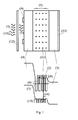
- Figure 1 shows its basic structure. It consists of a semiconductor region (1) with quantum dots (11) embed in it and sandwiched by two semiconductor regions, called “emitters". One of these emitters is of p type (4) and the other is of n type (3). Metal contacts, (9) and (10), are placed on these emitters. The contact located at the front side (9), that is, the side to receive the IR radiation (5), must not cover completely this area in order to allow radiation to come through. Typically, it should get the form of a grid.
- dots (11) The material that constitutes the dots (11) is called “dot material” and the material that surrounds it, “barrier material” (2). These are made of different semiconductors, characterised usually by different gaps. When properly chosen, they can lead to a simplified band diagram, also in Figure 1, but with some more detail in Figure 4.
- the band structure plotted is characterised by the appearance of an energy barrier for electrons in the conduction band.
- the height of this barrier (29) is known as depth of the potential well nevertheless quantum dots, wires or wells are being described.
- this invention will work also if the confinement potential is created in the valence band.
- the example chosen for illustration purposes is known as type I heterostructure, but other heterostructure types, like type II, can also work as far as this invention is concerned.
- Type II heterostructures are characterised by the conduction band of the dot material falls below the valence band of the barrier material or the conduction band of the barrier material falls below the valence band material.
- dots implies that the barrier material completely surrounds the dot material.
- the small dimension of the dots causes the quantum confinement of the electrons in the dot.
- This confinement is characterised because only a few energy levels (7) are allowed for electrons in the range of energies that compromises the potential well (29). If the dot is sufficiently small, it is possible to reach the ideal situation in which only one of these energy levels exist. With intrinsic semiconductor materials being used and in equilibrium conditions, these energy levels will be emptied of electrons. As far as this invention is concerned, it is necessary this energy levels are not emptied of electrons.
- the barrier (11) is n doped so that by the physical effect known as modulated doping, the electron is transferred from the impurity to this confined state.
- Doping density should be in the order of the dot density. A much higher doping could fill states in the conduction band and therefore, degrade photon absorption since empty states in the conduction band are necessary to allocate the electrons pumped from the confined states. Conversely, a lower density can insufficiently fill the confined states and again prevent photon absorption due to the absence of electrons to be pumped to the conduction band. Doping within the dot can produce the same filling of the confined states with electrons. However, effectively doping in the dot is considered technologically more difficult than doping in the barrier.
- the structure of the QDIB-IR photodetector would have been based on electron confinement in the valence band instead of confinement in the conduction band, p type doping would be required, in the barrier region or in the dot regions with the same considerations than above, to supply with holes the confined states. This is due to the fact that, in this case, empty states would be required in the confined states to receive the electrons from the valence band pumped by the IR radiation.
- the collection of confined states in the dot leads to a band, particularly, if the dots are located in a periodic fashion.
- This band is known in the literature as intermediate band.
- this band is effectively separated from the conduction band, where "effectively" means that a zero density of states exist between both, the use of quantum dots is a must.
- Our invention requires a zero density of states between the intermediate band and the conduction band. Quantum wells or wires do not provide such zero density of states.
- Conduction, intermediate and valence band have their own quasi-Fermi level to describe the electron population in each of them, to know, conduction band quasi-Fermi level (30), intermediate band quasi-Fermi level (31) and valence band quasi-Fermi level (32). With a high dot density, the quasi-Fermi level related to the intermediate band (31) can remain clamped to its equilibrium position, which is that of the intermediate band, even when the device becomes biased or illuminated.
- the wavelength of the IR radiation that will become effectively detected by this detector is that whose energy is in the order of the energy that separates the intermediate band (7) from the conduction band (8).
- the detector When an infrared photon impinges in the detector and is absorbed, it causes an electronic transition (6) from the intermediate band (7) to the conduction band (8), a process usually known as inter-subband transition. To detect this absorption process, and therefore, to detect the incident IR radiation, the detector can be operated both in voltage mode as in current mode.
- FIG. 5 shows the simplified bandgap diagram of the device operating under these conditions.
- the transition of electrons from the intermediate band to the conduction band (8) rises up the quasi-Fermi level of electrons in the conduction band (30).
- thermal process pump electrons from the valence band to the intermediate band (34) As it is known, in equilibrium, these processes are exactly balanced by the reverse ones or recombination processes (35).
- IR radiation promotes electrons from the intermediate band to the conduction band, equilibrium is broken and the valence band quasi-Fermi level (32) also rises up above the intermediate band quasi-Fermi level (31).
- the difference in the value between conduction and valence band quasi-Fermi levels becomes the output photovoltage (36) of the device multiplied by the electron charge.
- the photodetector is short-circuited ( Figure 6).
- the absorption of IR photons also causes electronic transitions from the intermediate band to the conduction band (6) and rises up the conduction band quasi-Fermi level (30) as in the case before.
- the output voltage is cero and the valence band quasi-Fermi level (32) equals the electron one.
- the recombination of electrons (35) between the intermediate band and the valence band is reduced and a current is extracted that is limited by the thermal generation (34) between the valence band and the intermediate band. This current is extracted as electrons (36) that exit the n contact and that equal the number of holes per unit of time that exit the p contact (37).
- the QDIB-IR detector shares with low bandgap photodetectors its operation in the photovoltage mode, and therefore, a potential for a higher detectivity that can allow their operation at room temperature where other IR detectors require cooling. It shares with the IR detectors based on conductivity change, also making use of low dimensional structures, the fact that its threshold bandgap for IR absorption can be tuned as the dimensions of the dots are changed. Both advantages are now combined in our device that also has the advantage of being capable of detecting light at normal incidence.
- a low energy band-pass filter (12) should be located in front of the side receiving the radiation.
- detectivity improves if no current (or voltage) is obtained from the device when it is not illuminated with the radiation to detect.
- this filter should blockade the pass of photons with energy higher or equal than the gap that separates the intermediate band from the valence band (38).
- the filter (12) could be removed.
- some dark current would be extracted from the device since, in addition to the mechanisms described above, external non infrared illumination could pump electrons directly from the valence band to the conduction band (14).
- the emitters are not only of the same type (21) (say n type) but must have a bandgap lower than the barrier material, our invention works better if the emitters have a higher bandgap.
- a higher bandgap decreases the recombination in the emitters and therefore improves (decreases) the dark current of the device. This translates into a higher gain of the photodetector.
- the device could also be operated at a reverse bias. This would be, however, at the cost of sacrificing some detectivity of the device. This is because, again, a reverse saturation current would be extracted from the device even when no IR radiation is present, having its physical origin in the thermal generation processes between bands as, for example, those taking place between the valence band and the conduction band.
- this band bending in the space charge regions also modifies the shape of the confining potential of the dots and therefore the position of the energy levels. This increases the difficulty to engineer the detection wavelength.
- conventional p (41) and n (40) semiconductor layers could be inserted adjacent to the emitters to sustain the band bending of the corresponding space charge regions instead of the region with quantum dots (1). We call these layers "damping" layers.
- An IR reflector (42) could also be located at the rear side of the device to reflect back to the quantum dot region the photons that have not been absorbed.
- the back contact (10) should also take the form of a grid.
- These contacting layers, made of a wide bandgap semiconductor would be in theory transparent to IR radiation and therefore, there would be no harm would they cover completely the front side of the emitter rather than being restricted to the regions underneath the metal contacts. In practice, it might not be the case since their high doping might cause free electron absorption processes to turn them into IR absorbers.
- the emitters take the form of layers. It is only necessary that at least a p and an n region exist. It is possible to take advantage from this fact as shown, for example, in Figure 8 where the p emitter (45) has been reduced to occupy the region underneath the contacts. The surface of the now completely exposed to IR radiation quantum dot region (1) should be passivated (46).
- This geometry also takes the advantage from the fact that the current extracted from the detector is small so that a some higher series resistance than in other optoelectronic devices, like for example solar cells, can be tolerated, furthermore if the device is operated in the voltage mode.
- a 0.1 ⁇ m GaAs n + type (10 18 cm -3 , silicon doped) buffer layer (49) is grown in a molecular beam epitaxy (MBE) system over a n type (5 ⁇ 10 17 cm -3 ) substrate (50).
- MBE molecular beam epitaxy
- This layer (49) will also act as back surface field layer to reduce back surface recombination.
- the following layers are grown on top:
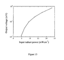
- Devices fabricated according to the recipe above have been manufactured and tested as IR photodetectors both in the current as in the voltage mode. For doing so, they were illuminated at normal incidence with a black body source at 850 C filtered by a 400 ⁇ m GaSb unintentionally doped wafer that plays the role of the filter (12). This filter blockades radiation below 1700 nm. Devices were operated at room temperature. Results are shown in Figure 12 (current mode) and Figure 13 (voltage mode) and demonstrate the operation of the devices as IR photodetectors.
- the QDIB-IR photodetector can be used to detect infrared radiation, both in the long-wavelength infrared region (1-30 microns) as in the far-infrared region (more than 30 microns) depending on the dot size. This capability to detect infrared light makes them suitable for manufacturing gas and molecule analyzers, flame detectors, and thermographic cameras.
- the QDIB-IR detector is used together with an infrared source and a monochromator.
- the monochromator scans the infrared source and focuses its output into the detector.
- the gas or dilution containing the molecules to be analyzed is inserted in-between this output and the detector.
- no test sample might have been inserted in order to set the reference for the measurement.
- the QDIB-IR would continuously monitor the subject under surveillance. When a fire starts, the phenomena is followed by a rising in the temperature and therefore, by an increase in the amount of infrared radiation that the QDIB-IR will detect. Without having an actual fire or flame, the QDIB-IR can also be used for contactless temperature measurements.
- the QDIB-IR can detect radiation for incidence normal to the plane of growth
- an array of these devices can be integrated in the same wafer to constitute the pixels of an imagining device.
- some of the photodectors in the array can be designed to detect mainly radiation at a given wavelength while others are at a different one. In this way, a multi-color array could be fabricated. Either way, the array will constitute the basic element of a thermographic camera with military (detection of targets) and medical applications (identification of harmed tissues). The use of QDIB-IR will also relax the need of detector cooling.
Landscapes
- Engineering & Computer Science (AREA)
- Chemical & Material Sciences (AREA)
- Nanotechnology (AREA)
- Physics & Mathematics (AREA)
- Crystallography & Structural Chemistry (AREA)
- Mathematical Physics (AREA)
- Theoretical Computer Science (AREA)
- Life Sciences & Earth Sciences (AREA)
- Biophysics (AREA)
- Optics & Photonics (AREA)
- Light Receiving Elements (AREA)
- Photometry And Measurement Of Optical Pulse Characteristics (AREA)
Applications Claiming Priority (1)
| Application Number | Priority Date | Filing Date | Title |
|---|---|---|---|
| ES200501296A ES2297972A1 (es) | 2005-05-30 | 2005-05-30 | Fotodetector de infrarrojos de banda intermedia y puntos cuanticos. |
Publications (2)
| Publication Number | Publication Date |
|---|---|
| EP1729347A2 true EP1729347A2 (de) | 2006-12-06 |
| EP1729347A3 EP1729347A3 (de) | 2008-01-16 |
Family
ID=36660159
Family Applications (1)
| Application Number | Title | Priority Date | Filing Date |
|---|---|---|---|
| EP06380115A Withdrawn EP1729347A3 (de) | 2005-05-30 | 2006-05-17 | Quantenpunktinfrarotdetektor mit Zwischenenergieband |
Country Status (3)
| Country | Link |
|---|---|
| US (1) | US20060266998A1 (de) |
| EP (1) | EP1729347A3 (de) |
| ES (1) | ES2297972A1 (de) |
Cited By (2)
| Publication number | Priority date | Publication date | Assignee | Title |
|---|---|---|---|---|
| US7915521B2 (en) | 2007-10-10 | 2011-03-29 | The Trustees Of Princeton University | Type II quantum dot solar cells |
| US8927852B2 (en) | 2008-08-21 | 2015-01-06 | Seagate Technology Llc | Photovoltaic device with an up-converting quantum dot layer and absorber |
Families Citing this family (22)
| Publication number | Priority date | Publication date | Assignee | Title |
|---|---|---|---|---|
| US7745900B2 (en) * | 2005-08-24 | 2010-06-29 | Micron Technology, Inc. | Method and apparatus providing refractive index structure for a device capturing or displaying images |
| ES2276624B2 (es) * | 2005-12-13 | 2008-03-16 | Universidad Politecnica De Madrid | Metodo para la supresion de la recombinacion no radiativa en materiales dopados con centros profundos. |
| US7750425B2 (en) * | 2005-12-16 | 2010-07-06 | The Trustees Of Princeton University | Intermediate-band photosensitive device with quantum dots embedded in energy fence barrier |
| US11245048B2 (en) * | 2006-03-19 | 2022-02-08 | Shimon Maimon | Reduced dark current photodetector with charge compensated barrier layer |
| US11264528B2 (en) * | 2006-03-19 | 2022-03-01 | Shimon Maimon | Reduced dark current photodetector with charge compensated barrier layer |
| KR101513406B1 (ko) * | 2006-09-29 | 2015-04-17 | 유니버시티 오브 플로리다 리서치 파운데이션, 인크. | 적외선 감지 및 표시를 위한 방법 및 장치 |
| JP5364526B2 (ja) * | 2009-10-02 | 2013-12-11 | 三菱重工業株式会社 | 赤外線検出素子、赤外線検出装置及び赤外線検出素子の製造方法 |
| AU2011258475A1 (en) | 2010-05-24 | 2012-11-15 | Nanoholdings, Llc | Method and apparatus for providing a charge blocking layer on an infrared up-conversion device |
| RU2013139232A (ru) * | 2011-02-28 | 2015-04-10 | Юниверсити Оф Флорида Рисеч Фаундэйшн, Инк. | Устройства преобразования с повышением частоты, содержащие широкополосный поглотитель |
| US10170652B2 (en) * | 2011-03-22 | 2019-01-01 | The Boeing Company | Metamorphic solar cell having improved current generation |
| CN103733355B (zh) | 2011-06-30 | 2017-02-08 | 佛罗里达大学研究基金会有限公司 | 用于检测红外辐射的带有增益的方法和设备 |
| RU2503090C1 (ru) * | 2012-05-29 | 2013-12-27 | Лариса Викторовна Арапкина | Способ детектирования электромагнитного излучения и устройство для его осуществления |
| FR2992470B1 (fr) * | 2012-06-26 | 2014-08-08 | Commissariat Energie Atomique | Element photodetecteur pour une radiation lumineuse infrarouge et photodetecteur comprenant un tel element photodetecteur |
| US10566491B2 (en) * | 2013-02-12 | 2020-02-18 | The George Washington University | Solar cell using quantum dots and method of fabricating same |
| US8952478B2 (en) * | 2013-04-24 | 2015-02-10 | Infineon Technologies Austria Ag | Radiation conversion device and method of manufacturing a radiation conversion device |
| US9941433B2 (en) * | 2014-12-11 | 2018-04-10 | Vadient Optics, Llc | Composite quantum-dot materials for photonic detectors |
| KR101660163B1 (ko) * | 2015-02-04 | 2016-09-26 | 엘지전자 주식회사 | 광 변환 부재, 이를 포함하는 백라이트 유닛 및 디스플레이 장치 |
| CA2988784A1 (en) | 2015-06-11 | 2017-03-09 | University Of Florida Research Foundation, Incorporated | Monodisperse, ir-absorbing nanoparticles and related methods and devices |
| CN105720130B (zh) * | 2015-07-10 | 2018-01-30 | 中国科学院物理研究所 | 基于量子阱带间跃迁的光电探测器 |
| CN106847952A (zh) * | 2016-12-14 | 2017-06-13 | 中国科学院上海微系统与信息技术研究所 | 一种Si基三维Ge量子点晶体光伏型近中红外双色探测器 |
| EP3586378A4 (de) * | 2017-02-24 | 2020-09-30 | The Government of the United States of America, as represented by the Secretary of the Navy | Kapazitiver infrarotphotodetektor |
| CN113281833B (zh) * | 2021-05-10 | 2023-03-10 | 姜泽 | 一种薄镜片优面形红外带通滤光片及制作方法 |
Citations (8)
| Publication number | Priority date | Publication date | Assignee | Title |
|---|---|---|---|---|
| US17176A (en) | 1857-04-28 | Self-adjusting- sack-holdeb | ||
| US94597A (en) | 1869-09-07 | Improved breast-loop for hames | ||
| US136909A (en) | 1873-03-18 | Improvement in washing-machines | ||
| US6239449B1 (en) | 1998-05-05 | 2001-05-29 | National Research Council Of Canada | Quantum dot infrared photodetectors (QDIP) |
| US6452242B1 (en) | 2000-03-23 | 2002-09-17 | Mp Technologies Llc | Multi color detector |
| US6531700B1 (en) | 1998-09-08 | 2003-03-11 | Lockheed Martin Corporation | Integral charge well for QWIP FPA'S |
| US6642537B1 (en) | 1996-08-27 | 2003-11-04 | California Institute Of Technology | Dual band QWIP focal plane array |
| US6657195B1 (en) | 2000-09-21 | 2003-12-02 | Lockheed Martin Corporation | Clutter discriminating focal plane arrays |
Family Cites Families (13)
| Publication number | Priority date | Publication date | Assignee | Title |
|---|---|---|---|---|
| US5936258A (en) * | 1995-04-28 | 1999-08-10 | Fujitsu Limited | Optical semiconductor memory device and read/write method therefor |
| JPH10326906A (ja) * | 1997-05-26 | 1998-12-08 | Hamamatsu Photonics Kk | 光検出素子及び撮像素子 |
| GB2353635B (en) * | 1999-07-10 | 2002-03-20 | Toshiba Res Europ Ltd | Optical device |
| KR100313889B1 (ko) * | 1999-03-31 | 2001-11-17 | 구자홍 | 양자점 적외선 수광소자 및 그 제조방법 |
| ES2149137B1 (es) * | 1999-06-09 | 2001-11-16 | Univ Madrid Politecnica | Celula solar fotovoltaica de semiconductor de banda intermedia. |
| US6346431B1 (en) * | 2000-07-10 | 2002-02-12 | Lg Electronics Inc. | Quantum dot infrared detection device and method for fabricating the same |
| AUPQ897600A0 (en) * | 2000-07-25 | 2000-08-17 | Liddiard, Kevin | Active or self-biasing micro-bolometer infrared detector |
| JP3753605B2 (ja) * | 2000-11-01 | 2006-03-08 | シャープ株式会社 | 太陽電池およびその製造方法 |
| TW480591B (en) * | 2001-01-15 | 2002-03-21 | Nat Science Council | Manufacture method of quantum dot infrared sensor |
| US20030136909A1 (en) * | 2002-01-23 | 2003-07-24 | James Plante | High temperature quantum well photodetectors |
| JP4040970B2 (ja) * | 2002-12-27 | 2008-01-30 | 独立行政法人科学技術振興機構 | 中赤外光子検出器 |
| US6906326B2 (en) * | 2003-07-25 | 2005-06-14 | Bae Systems Information And Elecronic Systems Integration Inc. | Quantum dot infrared photodetector focal plane array |
| KR20050019484A (ko) * | 2003-08-19 | 2005-03-03 | 삼성전자주식회사 | 광검출소자가 일체적으로 성장된 장파장 수직 면발광 레이저 |
-
2005
- 2005-05-30 ES ES200501296A patent/ES2297972A1/es active Pending
-
2006
- 2006-05-17 EP EP06380115A patent/EP1729347A3/de not_active Withdrawn
- 2006-05-26 US US11/441,034 patent/US20060266998A1/en not_active Abandoned
Patent Citations (8)
| Publication number | Priority date | Publication date | Assignee | Title |
|---|---|---|---|---|
| US17176A (en) | 1857-04-28 | Self-adjusting- sack-holdeb | ||
| US94597A (en) | 1869-09-07 | Improved breast-loop for hames | ||
| US136909A (en) | 1873-03-18 | Improvement in washing-machines | ||
| US6642537B1 (en) | 1996-08-27 | 2003-11-04 | California Institute Of Technology | Dual band QWIP focal plane array |
| US6239449B1 (en) | 1998-05-05 | 2001-05-29 | National Research Council Of Canada | Quantum dot infrared photodetectors (QDIP) |
| US6531700B1 (en) | 1998-09-08 | 2003-03-11 | Lockheed Martin Corporation | Integral charge well for QWIP FPA'S |
| US6452242B1 (en) | 2000-03-23 | 2002-09-17 | Mp Technologies Llc | Multi color detector |
| US6657195B1 (en) | 2000-09-21 | 2003-12-02 | Lockheed Martin Corporation | Clutter discriminating focal plane arrays |
Cited By (2)
| Publication number | Priority date | Publication date | Assignee | Title |
|---|---|---|---|---|
| US7915521B2 (en) | 2007-10-10 | 2011-03-29 | The Trustees Of Princeton University | Type II quantum dot solar cells |
| US8927852B2 (en) | 2008-08-21 | 2015-01-06 | Seagate Technology Llc | Photovoltaic device with an up-converting quantum dot layer and absorber |
Also Published As
| Publication number | Publication date |
|---|---|
| EP1729347A3 (de) | 2008-01-16 |
| US20060266998A1 (en) | 2006-11-30 |
| ES2297972A1 (es) | 2008-05-01 |
Similar Documents
| Publication | Publication Date | Title |
|---|---|---|
| EP1729347A2 (de) | Quantenpunktinfrarotdetektor mit Zwischenenergieband | |
| US9472697B2 (en) | Photodetector with surface plasmon resonance | |
| US7271405B2 (en) | Intersubband detector with avalanche multiplier region | |
| Stiff et al. | High-detectivity, normal-incidence, mid-infrared (λ∼ 4 μm) InAs/GaAs quantum-dot detector operating at 150 K | |
| EP3072161B1 (de) | Zweifarbdetektor zur erweiterung eines resonanten hohlraums zur leistungsverbesserung | |
| Zhou et al. | Progress in quantum well and quantum cascade infrared photodetectors in SITP | |
| JP4856031B2 (ja) | アバランシェフォトダイオード | |
| US5567955A (en) | Method for infrared thermal imaging using integrated gasa quantum well mid-infrared detector and near-infrared light emitter and SI charge coupled device | |
| Liu et al. | High Temperature Behaviors of 1–2.5 μm Extended Wavelength In₀. ₈₃Ga₀. ₁₇As Photodetectors on InP Substrate | |
| WO2014064930A1 (en) | High operating temperature resonant tunnelling quantum well photodetector | |
| Mazzeo et al. | AlGaN-based linear array for UV solar-blind imaging from 240 to 280 nm | |
| Bansal et al. | Photodetectors for security application | |
| Buffaz et al. | State of the art of quantum cascade photodetectors | |
| Krishna et al. | Hot Dot Detectors. Infrared Quantum Dot Intersubband Photodetectors Are a Promising Technology for Multiwavelength IR Detection | |
| Perera | Quantum structures for multiband photon detection | |
| JP2773930B2 (ja) | 光検知装置 | |
| Gunapala et al. | infrared photodetector focal plane | |
| US8513704B2 (en) | Method for manufacturing a photodiode and corresponding photodiode and electromagnetic radiation detector | |
| Suo et al. | Dark Current Analysis of InAsSb-Based Hetero-$ p {\text {-}} i {\text {-}} n $ Mid-Infrared Photodiode | |
| Butyagin et al. | AlGaAs/GaAs multiquantum-well heterostructures for long-wavelength (8–10 μm) IR photodetectors | |
| Wehner et al. | Resonant cavity-enhanced mercury cadmium telluride detectors | |
| Pernot et al. | Improvement of Low‐Intensity Ultraviolet Photodetectors Based on AlGaN with Low Threading Dislocation Density | |
| Ji | Characterisation of AlInAsSb photodiodes and type-II InGaAs/GaAsSb superlattice photodiodes | |
| Plis et al. | Lateral diffusion of minority carriers in InAsSb-based nBn detectors | |
| Klimov et al. | Room temperature mid-IR two-color photodiodes with InAs and InAs0. 9Sb0. 1 absorbing layers |
Legal Events
| Date | Code | Title | Description |
|---|---|---|---|
| PUAI | Public reference made under article 153(3) epc to a published international application that has entered the european phase |
Free format text: ORIGINAL CODE: 0009012 |
|
| 17P | Request for examination filed |
Effective date: 20060517 |
|
| AK | Designated contracting states |
Kind code of ref document: A2 Designated state(s): AT BE BG CH CY CZ DE DK EE ES FI FR GB GR HU IE IS IT LI LT LU LV MC NL PL PT RO SE SI SK TR |
|
| AX | Request for extension of the european patent |
Extension state: AL BA HR MK YU |
|
| RIC1 | Information provided on ipc code assigned before grant |
Ipc: H01L 31/0304 20060101ALI20071025BHEP Ipc: H01L 27/144 20060101ALI20071025BHEP Ipc: H01L 31/101 20060101ALI20071025BHEP Ipc: H01L 31/0352 20060101AFI20060907BHEP |
|
| PUAL | Search report despatched |
Free format text: ORIGINAL CODE: 0009013 |
|
| AK | Designated contracting states |
Kind code of ref document: A3 Designated state(s): AT BE BG CH CY CZ DE DK EE ES FI FR GB GR HU IE IS IT LI LT LU LV MC NL PL PT RO SE SI SK TR |
|
| AX | Request for extension of the european patent |
Extension state: AL BA HR MK YU |
|
| AKX | Designation fees paid |
Designated state(s): AT BE BG CH CY CZ DE DK EE ES FI FR GB GR HU IE IS IT LI LT LU LV MC NL PL PT RO SE SI SK TR |
|
| 17Q | First examination report despatched |
Effective date: 20080909 |
|
| STAA | Information on the status of an ep patent application or granted ep patent |
Free format text: STATUS: THE APPLICATION IS DEEMED TO BE WITHDRAWN |
|
| 18D | Application deemed to be withdrawn |
Effective date: 20090120 |