EP1729337A2 - Electronic device and method of manufacturing the same - Google Patents
Electronic device and method of manufacturing the same Download PDFInfo
- Publication number
- EP1729337A2 EP1729337A2 EP06252847A EP06252847A EP1729337A2 EP 1729337 A2 EP1729337 A2 EP 1729337A2 EP 06252847 A EP06252847 A EP 06252847A EP 06252847 A EP06252847 A EP 06252847A EP 1729337 A2 EP1729337 A2 EP 1729337A2
- Authority
- EP
- European Patent Office
- Prior art keywords
- substrate
- solder
- electronic device
- packaging part
- packaging
- Prior art date
- Legal status (The legal status is an assumption and is not a legal conclusion. Google has not performed a legal analysis and makes no representation as to the accuracy of the status listed.)
- Withdrawn
Links
Images





Classifications
-
- H—ELECTRICITY
- H05—ELECTRIC TECHNIQUES NOT OTHERWISE PROVIDED FOR
- H05K—PRINTED CIRCUITS; CASINGS OR CONSTRUCTIONAL DETAILS OF ELECTRIC APPARATUS; MANUFACTURE OF ASSEMBLAGES OF ELECTRICAL COMPONENTS
- H05K3/00—Apparatus or processes for manufacturing printed circuits
- H05K3/22—Secondary treatment of printed circuits
- H05K3/28—Applying non-metallic protective coatings
- H05K3/284—Applying non-metallic protective coatings for encapsulating mounted components
-
- H—ELECTRICITY
- H10—SEMICONDUCTOR DEVICES; ELECTRIC SOLID-STATE DEVICES NOT OTHERWISE PROVIDED FOR
- H10W—GENERIC PACKAGES, INTERCONNECTIONS, CONNECTORS OR OTHER CONSTRUCTIONAL DETAILS OF DEVICES COVERED BY CLASS H10
- H10W72/00—Interconnections or connectors in packages
- H10W72/20—Bump connectors, e.g. solder bumps or copper pillars; Dummy bumps; Thermal bumps
-
- H—ELECTRICITY
- H05—ELECTRIC TECHNIQUES NOT OTHERWISE PROVIDED FOR
- H05K—PRINTED CIRCUITS; CASINGS OR CONSTRUCTIONAL DETAILS OF ELECTRIC APPARATUS; MANUFACTURE OF ASSEMBLAGES OF ELECTRICAL COMPONENTS
- H05K3/00—Apparatus or processes for manufacturing printed circuits
- H05K3/30—Assembling printed circuits with electric components, e.g. with resistors
- H05K3/303—Assembling printed circuits with electric components, e.g. with resistors with surface mounted components
- H05K3/305—Affixing by adhesive
-
- H—ELECTRICITY
- H05—ELECTRIC TECHNIQUES NOT OTHERWISE PROVIDED FOR
- H05K—PRINTED CIRCUITS; CASINGS OR CONSTRUCTIONAL DETAILS OF ELECTRIC APPARATUS; MANUFACTURE OF ASSEMBLAGES OF ELECTRICAL COMPONENTS
- H05K3/00—Apparatus or processes for manufacturing printed circuits
- H05K3/30—Assembling printed circuits with electric components, e.g. with resistors
- H05K3/32—Assembling printed circuits with electric components, e.g. with resistors electrically connecting electric components or wires to printed circuits
- H05K3/34—Assembling printed circuits with electric components, e.g. with resistors electrically connecting electric components or wires to printed circuits by soldering
- H05K3/341—Surface mounted components
- H05K3/3431—Leadless components
- H05K3/3442—Leadless components having edge contacts, e.g. leadless chip capacitors, chip carriers
-
- H—ELECTRICITY
- H05—ELECTRIC TECHNIQUES NOT OTHERWISE PROVIDED FOR
- H05K—PRINTED CIRCUITS; CASINGS OR CONSTRUCTIONAL DETAILS OF ELECTRIC APPARATUS; MANUFACTURE OF ASSEMBLAGES OF ELECTRICAL COMPONENTS
- H05K3/00—Apparatus or processes for manufacturing printed circuits
- H05K3/30—Assembling printed circuits with electric components, e.g. with resistors
- H05K3/32—Assembling printed circuits with electric components, e.g. with resistors electrically connecting electric components or wires to printed circuits
- H05K3/34—Assembling printed circuits with electric components, e.g. with resistors electrically connecting electric components or wires to printed circuits by soldering
- H05K3/3452—Solder masks
-
- H—ELECTRICITY
- H05—ELECTRIC TECHNIQUES NOT OTHERWISE PROVIDED FOR
- H05K—PRINTED CIRCUITS; CASINGS OR CONSTRUCTIONAL DETAILS OF ELECTRIC APPARATUS; MANUFACTURE OF ASSEMBLAGES OF ELECTRICAL COMPONENTS
- H05K2201/00—Indexing scheme relating to printed circuits covered by H05K1/00
- H05K2201/09—Shape and layout
- H05K2201/09818—Shape or layout details not covered by a single group of H05K2201/09009 - H05K2201/09809
- H05K2201/0989—Coating free areas, e.g. areas other than pads or lands free of solder resist
-
- H—ELECTRICITY
- H05—ELECTRIC TECHNIQUES NOT OTHERWISE PROVIDED FOR
- H05K—PRINTED CIRCUITS; CASINGS OR CONSTRUCTIONAL DETAILS OF ELECTRIC APPARATUS; MANUFACTURE OF ASSEMBLAGES OF ELECTRICAL COMPONENTS
- H05K2201/00—Indexing scheme relating to printed circuits covered by H05K1/00
- H05K2201/09—Shape and layout
- H05K2201/09818—Shape or layout details not covered by a single group of H05K2201/09009 - H05K2201/09809
- H05K2201/099—Coating over pads, e.g. solder resist partly over pads
-
- H—ELECTRICITY
- H05—ELECTRIC TECHNIQUES NOT OTHERWISE PROVIDED FOR
- H05K—PRINTED CIRCUITS; CASINGS OR CONSTRUCTIONAL DETAILS OF ELECTRIC APPARATUS; MANUFACTURE OF ASSEMBLAGES OF ELECTRICAL COMPONENTS
- H05K2201/00—Indexing scheme relating to printed circuits covered by H05K1/00
- H05K2201/10—Details of components or other objects attached to or integrated in a printed circuit board
- H05K2201/10613—Details of electrical connections of non-printed components, e.g. special leads
- H05K2201/10621—Components characterised by their electrical contacts
- H05K2201/10636—Leadless chip, e.g. chip capacitor or resistor
-
- H—ELECTRICITY
- H05—ELECTRIC TECHNIQUES NOT OTHERWISE PROVIDED FOR
- H05K—PRINTED CIRCUITS; CASINGS OR CONSTRUCTIONAL DETAILS OF ELECTRIC APPARATUS; MANUFACTURE OF ASSEMBLAGES OF ELECTRICAL COMPONENTS
- H05K2201/00—Indexing scheme relating to printed circuits covered by H05K1/00
- H05K2201/10—Details of components or other objects attached to or integrated in a printed circuit board
- H05K2201/10613—Details of electrical connections of non-printed components, e.g. special leads
- H05K2201/10621—Components characterised by their electrical contacts
- H05K2201/10727—Leadless chip carrier [LCC], e.g. chip-modules for cards
-
- H—ELECTRICITY
- H05—ELECTRIC TECHNIQUES NOT OTHERWISE PROVIDED FOR
- H05K—PRINTED CIRCUITS; CASINGS OR CONSTRUCTIONAL DETAILS OF ELECTRIC APPARATUS; MANUFACTURE OF ASSEMBLAGES OF ELECTRICAL COMPONENTS
- H05K2201/00—Indexing scheme relating to printed circuits covered by H05K1/00
- H05K2201/10—Details of components or other objects attached to or integrated in a printed circuit board
- H05K2201/10613—Details of electrical connections of non-printed components, e.g. special leads
- H05K2201/10621—Components characterised by their electrical contacts
- H05K2201/10734—Ball grid array [BGA]; Bump grid array
-
- H—ELECTRICITY
- H05—ELECTRIC TECHNIQUES NOT OTHERWISE PROVIDED FOR
- H05K—PRINTED CIRCUITS; CASINGS OR CONSTRUCTIONAL DETAILS OF ELECTRIC APPARATUS; MANUFACTURE OF ASSEMBLAGES OF ELECTRICAL COMPONENTS
- H05K2201/00—Indexing scheme relating to printed circuits covered by H05K1/00
- H05K2201/10—Details of components or other objects attached to or integrated in a printed circuit board
- H05K2201/10613—Details of electrical connections of non-printed components, e.g. special leads
- H05K2201/10954—Other details of electrical connections
- H05K2201/10977—Encapsulated connections
-
- H—ELECTRICITY
- H05—ELECTRIC TECHNIQUES NOT OTHERWISE PROVIDED FOR
- H05K—PRINTED CIRCUITS; CASINGS OR CONSTRUCTIONAL DETAILS OF ELECTRIC APPARATUS; MANUFACTURE OF ASSEMBLAGES OF ELECTRICAL COMPONENTS
- H05K2201/00—Indexing scheme relating to printed circuits covered by H05K1/00
- H05K2201/20—Details of printed circuits not provided for in H05K2201/01 - H05K2201/10
- H05K2201/2036—Permanent spacer or stand-off in a printed circuit or printed circuit assembly
-
- H—ELECTRICITY
- H05—ELECTRIC TECHNIQUES NOT OTHERWISE PROVIDED FOR
- H05K—PRINTED CIRCUITS; CASINGS OR CONSTRUCTIONAL DETAILS OF ELECTRIC APPARATUS; MANUFACTURE OF ASSEMBLAGES OF ELECTRICAL COMPONENTS
- H05K2203/00—Indexing scheme relating to apparatus or processes for manufacturing printed circuits covered by H05K3/00
- H05K2203/13—Moulding and encapsulation; Deposition techniques; Protective layers
- H05K2203/1305—Moulding and encapsulation
- H05K2203/1316—Moulded encapsulation of mounted components
-
- H—ELECTRICITY
- H10—SEMICONDUCTOR DEVICES; ELECTRIC SOLID-STATE DEVICES NOT OTHERWISE PROVIDED FOR
- H10W—GENERIC PACKAGES, INTERCONNECTIONS, CONNECTORS OR OTHER CONSTRUCTIONAL DETAILS OF DEVICES COVERED BY CLASS H10
- H10W72/00—Interconnections or connectors in packages
- H10W72/90—Bond pads, in general
-
- H—ELECTRICITY
- H10—SEMICONDUCTOR DEVICES; ELECTRIC SOLID-STATE DEVICES NOT OTHERWISE PROVIDED FOR
- H10W—GENERIC PACKAGES, INTERCONNECTIONS, CONNECTORS OR OTHER CONSTRUCTIONAL DETAILS OF DEVICES COVERED BY CLASS H10
- H10W72/00—Interconnections or connectors in packages
- H10W72/90—Bond pads, in general
- H10W72/921—Structures or relative sizes of bond pads
- H10W72/923—Bond pads having multiple stacked layers
-
- H—ELECTRICITY
- H10—SEMICONDUCTOR DEVICES; ELECTRIC SOLID-STATE DEVICES NOT OTHERWISE PROVIDED FOR
- H10W—GENERIC PACKAGES, INTERCONNECTIONS, CONNECTORS OR OTHER CONSTRUCTIONAL DETAILS OF DEVICES COVERED BY CLASS H10
- H10W72/00—Interconnections or connectors in packages
- H10W72/90—Bond pads, in general
- H10W72/941—Dispositions of bond pads
- H10W72/9415—Dispositions of bond pads relative to the surface, e.g. recessed, protruding
-
- H—ELECTRICITY
- H10—SEMICONDUCTOR DEVICES; ELECTRIC SOLID-STATE DEVICES NOT OTHERWISE PROVIDED FOR
- H10W—GENERIC PACKAGES, INTERCONNECTIONS, CONNECTORS OR OTHER CONSTRUCTIONAL DETAILS OF DEVICES COVERED BY CLASS H10
- H10W74/00—Encapsulations, e.g. protective coatings
- H10W74/10—Encapsulations, e.g. protective coatings characterised by their shape or disposition
- H10W74/15—Encapsulations, e.g. protective coatings characterised by their shape or disposition on active surfaces of flip-chip devices, e.g. underfills
-
- H—ELECTRICITY
- H10—SEMICONDUCTOR DEVICES; ELECTRIC SOLID-STATE DEVICES NOT OTHERWISE PROVIDED FOR
- H10W—GENERIC PACKAGES, INTERCONNECTIONS, CONNECTORS OR OTHER CONSTRUCTIONAL DETAILS OF DEVICES COVERED BY CLASS H10
- H10W90/00—Package configurations
- H10W90/701—Package configurations characterised by the relative positions of pads or connectors relative to package parts
- H10W90/721—Package configurations characterised by the relative positions of pads or connectors relative to package parts of bump connectors
- H10W90/724—Package configurations characterised by the relative positions of pads or connectors relative to package parts of bump connectors between a chip and a stacked insulating package substrate, interposer or RDL
-
- Y—GENERAL TAGGING OF NEW TECHNOLOGICAL DEVELOPMENTS; GENERAL TAGGING OF CROSS-SECTIONAL TECHNOLOGIES SPANNING OVER SEVERAL SECTIONS OF THE IPC; TECHNICAL SUBJECTS COVERED BY FORMER USPC CROSS-REFERENCE ART COLLECTIONS [XRACs] AND DIGESTS
- Y02—TECHNOLOGIES OR APPLICATIONS FOR MITIGATION OR ADAPTATION AGAINST CLIMATE CHANGE
- Y02P—CLIMATE CHANGE MITIGATION TECHNOLOGIES IN THE PRODUCTION OR PROCESSING OF GOODS
- Y02P70/00—Climate change mitigation technologies in the production process for final industrial or consumer products
- Y02P70/50—Manufacturing or production processes characterised by the final manufactured product
-
- Y—GENERAL TAGGING OF NEW TECHNOLOGICAL DEVELOPMENTS; GENERAL TAGGING OF CROSS-SECTIONAL TECHNOLOGIES SPANNING OVER SEVERAL SECTIONS OF THE IPC; TECHNICAL SUBJECTS COVERED BY FORMER USPC CROSS-REFERENCE ART COLLECTIONS [XRACs] AND DIGESTS
- Y10—TECHNICAL SUBJECTS COVERED BY FORMER USPC
- Y10T—TECHNICAL SUBJECTS COVERED BY FORMER US CLASSIFICATION
- Y10T29/00—Metal working
- Y10T29/49—Method of mechanical manufacture
- Y10T29/49002—Electrical device making
- Y10T29/49117—Conductor or circuit manufacturing
- Y10T29/49124—On flat or curved insulated base, e.g., printed circuit, etc.
- Y10T29/4913—Assembling to base an electrical component, e.g., capacitor, etc.
-
- Y—GENERAL TAGGING OF NEW TECHNOLOGICAL DEVELOPMENTS; GENERAL TAGGING OF CROSS-SECTIONAL TECHNOLOGIES SPANNING OVER SEVERAL SECTIONS OF THE IPC; TECHNICAL SUBJECTS COVERED BY FORMER USPC CROSS-REFERENCE ART COLLECTIONS [XRACs] AND DIGESTS
- Y10—TECHNICAL SUBJECTS COVERED BY FORMER USPC
- Y10T—TECHNICAL SUBJECTS COVERED BY FORMER US CLASSIFICATION
- Y10T29/00—Metal working
- Y10T29/49—Method of mechanical manufacture
- Y10T29/49002—Electrical device making
- Y10T29/49117—Conductor or circuit manufacturing
- Y10T29/49169—Assembling electrical component directly to terminal or elongated conductor
- Y10T29/49171—Assembling electrical component directly to terminal or elongated conductor with encapsulating
Definitions
- the present disclosure relates to an electronic device and a method of manufacturing the same. More particularly, the present disclosure relates to an electronic device having such a structure that a packaging part is mounted on a substrate by using solder, and a method of manufacturing the same.
- FIG.18 shows an electronic device as a first related-art example.
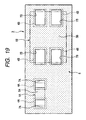
- FIG. 19 shows a substrate 3 used in the electronic device as the first related-art example. Foot patterns 4A, 4B onto which packaging parts 1A, 1B are soldered respectively are formed on a surface of the substrate 3. Also, various wiring patterns (not shown) as well as to the foot patterns 4A, 4B are formed on the surface of the substrate 3. A solder resist 5, 5A, 5B is formed on the surface of the substrate 3 to protect the wiring patterns.
- the solder resist 5, 5A, 5B is a resin having an insulating performance and, as shown in FIG.2, opening portions 7A, 7B are formed in positions opposing to the foot patterns 4A, 4B. Therefore, the foot patterns 4A, 4B are exposed from the solder resist 5 in positions in which the opening portions 7A, 7B are formed.
- the packaging parts 1A, 1B are surface-mounted on the foot patterns 4A, 4B, which are exposed from the opening portions 7A, 7B in the solder resist 5, with solder 6. More particularly, a packaging -part electrode 2A is provided to both side portions respectively because the packaging part 1A is a ceramic chip part. Also, the packaging part 1B is an electronic element such as an oscillator, or the like, and packaging part electrodes 2B are formed on a lower surface of the packaging part 1B.
- the solder paste is applied previously to the foot patterns 4A, 4B, and then the packaging parts 1A, 1B are mounted on the substrate 3 such that respective electrodes 2A, 2B are positioned on the foot patterns 4A, 4B to which the solder paste is applied. Then, the packaging parts 1A, 1B are surface-mounted on the substrate 3 with solder 6 by executing the reflow process under this condition.
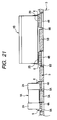
- An electronic device shown in FIG.21 has the almost same structure as the electronic device shown in FIG.18.
- the electronic device shown in FIG.18 is constructed in such a manner that areas of the opening portions 7A, 7B formed in the solder resist 5 are smaller than areas of the foot patterns 4A, 4B respectively and that outer peripheral portions of the foot patterns 4A, 4B are covered with the solder resist 5.
- the electronic device shown in FIG.21 is constructed such that the areas of the opening portions 8A, 8B formed in the solder resist 5 are set larger than the areas of the foot patterns 4A, 4B respectively and thus overall areas of the foot patterns 4A, 4B are exposed from the solder resist 5 (see FIG. 22).
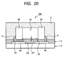
- the packaging parts are sealed with a sealing resin 9.
- the sealing resin 9 formed of an opaque resin makes it possible to prevent the arrangements and structures of the packaging parts 1A, 1B and the wiring patterns from being seen from the outside.
- a minute clearance (indicated with an arrow ⁇ h in respective Figures) is formed between the packaging part 1A, when mounted on the substrate 3, and the solder resist 5A, 5B.
- a magnitude of this clearance ⁇ h is varied due to a size of the packaging part 1A, an applied amount of the solder 6, and the like, and is given by almost 5 to 10 ⁇ m, for example.
- the disclosure below describes an electronic device capable of preventing not only generation of a short-circuit between electrode patterns during heating but also generation of cracks in a sealing resin by increasing an isolation distance between a packaging part and a substrate, and a method of manufacturing the same.
- An electronic device comprises:
- the solder resist when the substrate is viewed from a top, may have overlapping portions that are overlapped with areas in which the packaging part electrodes and the electrode patterns oppose to each other.
- the overlapping portions that are overlapped with areas where the packaging part electrodes and the electrode patterns oppose to each other are provided to the solder resist. Therefore, a part of the solder can be caused easily to run on the upper surface of the solder resist (overlapping portions).
- the solder resist may not be provided in an area in which the packaging part and the substrate oppose to each other.
- the packaging part opposes directly to the substrate and the solder resist is not present between them. Therefore, a height of the packaging part from the substrate can be set further large, and thus the sealing resin can be injected more surely into the spaces between the packaging part and the substrate.
- an electronic device .comprises:
- the buried member buried in the solder is provided into the electrode patterns respectively, the buried member is buried in the inside of the solder when the solder is applied to the electrode patterns. Therefore, a height of the solder is increased higher than a height obtained when the buried member is not provided. As a result, an isolation distance between the packaging part and the substrate can be set large and thus the sealing resin can be injected without fail into the spaces between the packaging part and the substrate.
- the buried member is formed of the solder resist.
- the buried member is formed of the solder resist. Therefore, the buried member can be formed at the same time when the solder resist is formed.
- the buried member is provided to areas in which the packaging part electrodes and the electrode patterns oppose to each other.
- the buried member is provided to the areas where the packaging part electrodes oppose to the electrode patterns. Therefore, the buried member can be provided without fail to the inside of the solder.
- a method of manufacturing an electronic device comprises: steps of applying solder to electrode patterns on a substrate on a surface of which the electrode patterns and a solder resist are provided such that the electrode patterns are exposed from opening portions formed in the solder resist; mounting packaging part electrodes, which are provided to a packaging part, on the electrode patterns by using the solder; and forming a sealing resin, which seals the packaging part, on the substrate; wherein, before the mounting step is executed, a thermosetting adhesive having an activation power necessary for soldering is provided to a position corresponding t.o a mounting position of the substrate, on which the packaging part is mounted.
- thermosetting adhesive having an activation power necessary for the soldering is provided before the mounting step is executed, the packaging part can be secured to the substrate by using this adhesive in the mounting step. Also, since the solder is activated by the activator contained in the adhesive when the packaging part is soldered to the wiring patterns in the mounting step, the soldering can be executed without fail. In addition, since the adhesive is present between the packaging part and the substrate in the sealing step, no clearance is generated between the packaging part and the substrate when the sealing resin is formed.
- Various implementations may include one or more the following advantages. For example, since an isolation distance between the packaging part and the substrate can be set large, the sealing resin can be introduced surely into the spaces between the packaging part and the substrate. Thus, even when the sealing resin is formed, no clearance is generated between the packaging part and the substrate. Therefore, it can be prevented that a short-circuit between the packaging parts patterns via the solder entered into the clearance is generated, and also it can be prevented that an air in the clearance is expanded by heating to exert a bad influence upon the sealing resin, and the like. As a result, reliability of the electronic device can be improved.
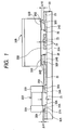
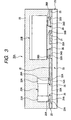
- FIG.1 to FIG. 3 are views explaining an electronic device 30A as a first embodiment of the present invention.
- FIG.1 is a side view showing a state before a sealing resin 29 is provided to the electronic device 30A
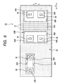
- FIG. 2 is a plan view of a substrate 23 constituting the electronic device 30A
- FIG.3 is a longitudinal sectional view of the electronic device 30A.
- the electronic device 30A comprises packaging parts 20A, 20B, the substrate 23, the sealing resin 29, and the like.
- the packaging part 20A is a ceramic chip parts such as a resistor, a capacitor, or the like, for example, and packaging part electrodes 22A are formed on both sides of the packaging part 20A.
- the packaging part 20B is an electronic element such as a SAW filter, an oscillator, or the like, for example, and packaging part electrocies 22B are formed on a lower surface of the packaging part 20B.
- the substrate 23 is a printed-wiring board, for example, and foot patterns 24A, 24B are formed on a surface of the substrate 23.
- the foot patterns 24A are the electrode patterns used to mount the packaging part 20A
- the foot patterns 24B are the electrode patterns used to mount the packaging parts 20.
- various wiring patterns 31 as well as the foot patterns 24A, 24B are formed on a surface of the substrate 23. In the present embodiment, the wiring patterns 31 are provided to positions that oppose to the packaging part 20B.
- a solder resist 25 is formed on the surface of the substrate 23 to protect the wiring patterns 31.
- the solder resist 25 is provided to the surface of the substrate 23 such that, when the solder is applied, solder 26 is not deposited on conductors (e.g., the wiring patterns 31) other than the foot patterns 24A, 24B.
- the solder resist 25 is formed relatively easily in a desired shape by the screen printing, or the like.
- opening portions 27A, 27B are formed in the solder resist 25.
- the opening portions 27A, 27B are formed to correspond to forming positions of the foot patterns 24A, 24B formed on the substrate 23. More particularly, the opening portion 27A is formed to correspond to the foot patterns 24A on which the packaging part 20A is mounted, and also the opening portions 27B are formed to correspond to the foot patterns 24B on which the packaging part 20B is mounted.
- a length L1 of the opening portion 27A in the arrow X direction in FIG. 2 is set shorter than a length L2 of the packaging part 20A (in FIG.2, its outer shape is indicated by a chain double-dashed line) in the arrow X direction in a mounted state (L2>L1).
- two opening portions 27B are formed on the right and left sides in FIG.2 to put a lower resist 25A of the packaging part 20B between them.
- a length L3 between a left end portion and a right end portion containing two opening portions 27B in FIG. 2 is set shorter than a length L4 of the packaging part 208 (in FIG.2, its outer shape is indicated by a chain double-dashed line) in the arrow X direction in a mounted state (L4>L3).
- the present embodiment is constructed such that a part of the foot patterns 24A, 24B is covered with the solder resist 25.
- a portion of the solder resist 25 for covering a part of the foot patterns 24A is referred to as an overlapping portion 32A and a portion of the solder resist 25 for covering a part of the foot patterns 24B is referred to as an overlapping portion 32B.
- Respective overlapping portions 32A, 32B are provided on outer positions of the foot patterns 24A, 24B.
- the overlapping portion 32A (32B) is provided to extend in the arrow X direction only in FIG.2, and a width dimension of the overlapping portion 32A is given by a width indicated by an arrow X1 (X2) in FIG.2.
- the overlapping portions 32A, 32B are constructed such that they are positioned in areas of the packaging parts 20A, 20B in their mounted state (areas indicated by a chain double-dashed line in FIG.2). In other words, the overlapping portions 32A, 32B are constructed to oppose to the packaging parts 20A, 20B when the packaging parts 20A, 20B are mounted on the substrate 23.
- the solder resist 25 located between a pair of foot patterns 24A, 24A is not provided. Therefore, as shown in FIG.1, the packaging part 20A is faced directly to the substrate 23 before it is sealed with the sealing resin 29.
- the wiring patterns 31 are provided between the left and right foot patterns 24B on the side where the packaging part 20B is provided.
- the lower resist 25A is formed between the left and right foot patterns 24B on the side where the packaging part 20B is provided.
- the solder paste is applied onto the foot patterns 24A, 24B to mount the packaging parts 20A, 20B on the substrate 23. At this time, the solder paste is applied onto not only upper surfaces of the foot patterns 24A, 24B but also upper surfaces of the overlapping portions 32A, 32B.
- the packaging parts 20A, 20B are aligned with the substrate 23 such that the electrodes 22A, 22B are positioned on the foot patterns 24A, 24B onto which the solder paste is applied, and then the packaging parts 20A, 20B are fitted onto the substrate 23. In this state, the packaging parts 20A, 20B are temporarily fitted to the substrate 23 by the solder paste.
- the substrate 23 to which the packaging parts 20A, 20B are temporarily fitted is put into the reflow furnace, and then the reflow process is carried out.
- organic components in the solder paste are evaporated and the solder is melted.
- the packaging part electrodes 22A, 22B of the packaging parts 20A, 20B are soldered to the foot patterns 24A, 24B with the solder 26 after the melted solder 26 is cooled/solidified.
- FIG.1 shows a state that the packaging -arts 20A, 20B are secured to the foot patterns 24A, 24B with the solder 26.
- the solder 26 in the present embodiment is mentioned hereunder.
- a part of the solder 26 is formed to run on the upper portion of the solder resist 25 (portion of the solder 26 formed to run on the upper portion of the solder resist 25 is referred to as running-on portions 26A, 26B respectively hereinafter).
- the packaging part 20A is positioned higher than the upper portion of the solder resist 25 by a thickness of the running-on portion 26A (indicated by an arrow ⁇ H1 in FIG.1) in its mounted state, and also the packaging part 20B is positioned higher than the upper portion of the solder resist 25 by a thickness of the running-on portion 26B (indicated by an arrow ⁇ H2 in FIG.1).
- the thicknesses ( ⁇ H1, ⁇ H2) of the running-on portions 26A, 26B can be adjusted by areas of the overlapping portions 32A, 32B overlapped on the foot patterns 24A, 24B (in other words, exposed areas of the foot patterns 24A, 24B), an applied amount of the solder 26, and the like.
- the running-on portion 26A, 26B solder resist 25 that has essentially a low affinity for the solder
- the overlapping portions 32A, 32B should be provided in areas that are overlapped with the areas where the packaging part electrodes 22A, 22B are opposed to the foot patterns 24A, 24B.
- the running-on portion 26A, 26B can be prevented from leaking out from outer peripheries of the packaging parts 20A, 20B to the outer side. Accordingly, the running-on portion 26A, 26B can be held between the packaging parts 20A, 20B and the substrate 23 (the foot patterns 24A, 24B, the overlapping portions 32A, 32B).
- the packaging parts 20A, 20B can be isolated more largely from the substrate 23 than the related art (see FIG.18 to FIG.23). More concretely, on the packaging side of the packaging part 20A, the solder resist 25 under the packaging position of the packaging part 20A is not provided. Thus, an isolation distance between the substrate 23 and the packaging part 20A is given by a distance indicated by an arrow Z1 in FIG.1.
- the lower resist 25A is formed between the packaging part 20B and the substrate 23 because of the presence of the wiring patterns 31.
- an isolation distance between a surface of the lower resist 25A and the lower surface of the packaging part 20B is given by a distance indicated by an arrow Z2 in FIG.1.
- isolation distances Z1, Z2 can be increased large rather than the related art ( ⁇ H indicated in FIG.20 and FIG.23).
- the isolation distances Z1 Z2 although varied due to the exposed area of the foot pattern 24A, an applied amount of the solder 26, etc., can be set to 20 ⁇ m to 30 ⁇ m, for example.
- the sealing resin 29 is formed to seal the packaging parts 20A, 20B provided onto the substrate 23.
- the sealing resin 29 is made of an epoxy resin, and is formed by using the transfer molding method, for example.
- the sealing resin 29 can be introduced without fail into spaces (33A, 33B) between the packaging parts 20A, 20B and the substrate 23.
- the sealing resin 29 can be introduced more surely because the solder resist 25 is not present between the packaging part 20A and the substrate 23.
- the sealing resin 29 is introduced into the spaces between the packaging parts 20A, 20B and the substrate 23, a clearance is never generated between the packaging parts 20A, 20B and the substrate 23. Therefore, even when the heating is applied upon mounting the electronic device 30A, and the like, a short-circuit between the foot patterns 24A, 24B via the solder 26 is never generated, and also the sealing resin 29 is never badly influenced by the expansion of the air in the clearance. As a result, reliability of the electronic device 30A can be improved.
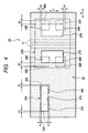
- FIG.4 shows the substrate 23 provided to an electronic device as a variation of the first embodiment of the present invention.
- the first embodiment shown in FIG.2 is constructed such that the overlapping portions 32A, 32B are provided to extend in the arrow X direction in FIG.2 only.
- this variation is characterized in that the overlapping portions 32A, 32B are provided to-extend not only in the arrow X direction in FIG.4 but also in the arrow Y direction in FIG.4.
- width dimensions of extended portions of the overlapping portions 32A, 32B in the arrow Y direction are set to widths indicated by arrows Y1, Y2 respectively.
- the forming positions of the overlapping portions 32A, 32B are not limited to one side of the foot patterns 24A, 24B, and they may be formed on two sides.
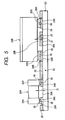
- FIG. 5 to FIG. 7 are views explaining an electronic device 30B as a second embodiment the present invention.
- the same reference symbols are affixed to the same configuration as the electronic device 30A according to the first embodiment shown in FIG. 1 to FIG.3, and their explanation will be omitted herein.
- the above electronic device 30A according to the first embodiment is characterized in that respective heights of the packaging parts 20A, 20B from the substrate 23 are increased since a part of the solder 26 is formed to run on the upper portion of the solder resist 25 to constitute the running-on portions 26A, 26B, and thus the sealing resin 29 can be introduced without fail into the spaces between the packaging parts 20A, 20B and the substrate 23.
- the electronic device 30B according to the present embodiment is characterized in that a buried member 35 is provided to the foot patterns 24A, 24B respectively.
- This buried member 35 is formed collectively upon forming the solder resist 25, and thus the buried member 35 is formed of the same material as the solder resist 25.
- the forming position of the buried member 35 is selected in almost center portions of the foot patterns 24A, 24B.
- the solder resist 25 can be formed easily by the screen printing, or the like, and printing (application) positions can be selected flexibly.
- the buried member 35 can be formed easily in the almost center portions of the foot patterns 24A, 24B. Also, since the buried member 35 is formed simultaneously with the solder resist 25, simplification of the manufacturing steps of the electronic device 30B can be achieved.
- the overlapping portions 32A, 32B are not provided on the foot patterns 24A, 24B. As shown in FIG.5 and FIG. 6, the foot patterns 24A, 24B are constructed to be exposed totally from opening portions 28A, 28B respectively.
- the packaging parts 20A, 20B are aligned with the substrate 23 such that respective electrodes 22A, 22B are positioned on the foot patterns 24A, 24B, and then the packaging parts 20A, 20B are mounted/fitted onto the substrate 23.
- the packaging parts 20A, 20B are temporarily fitted to the substrate 23 by the solder paste.
- the substrate 23 is put into the reflow furnace, and then the reflow process is carried out.
- organic components in the solder paste are evaporated and the solder is melted.
- the packaging part electrodes 22A, 22B of the packaging parts 20A, 20B are soldered to the foot patterns 24A, 24B with the solder 26 after the melted solder 26 is cooled/solidified.
- the buried member 35 is formed in the almost center portions of the foot patterns 24A, 24B respectively, the melted solder 26 will assume the shape close to a sphere because of a surface tension when the solder 26 is melted. Therefore, even though the buried member 35 is formed of the solder resist, such buried member 35 is positioned in the inside of the solder 26. Then, the buried member 35 is buried in the solder 26 after the solder 26 is cooled in this state.
- a height of the solder 26 is increased higher than that of the solder 26 obtained when the buried member 35 is not provided. That is, a height of the solder 26 is increased by a height that corresponds to a volume of the buried member 35. Therefore, in the electronic device 30B according to the present embodiment, an isolation distance between the packaging parts 20A, 20B and the substrate 23 can be set large, and thus the sealing resin 29 can be introduced surely into the spaces between the packaging parts 20A, 20B and the substrate 23.
- the clearance is never generated between the packaging parts 20A, 20B and the substrate 23. Therefore, even when the heating is applied upon mounting the electronic device 30B, and the like, a short-circuit between the foot patterns 24A, 24B via the solder 26 is never generated, and also the sealing resin 29 is never badly affected by the expansion of the air in the clearance. As a result, reliability of the electronic device 30B can be improved.
- FIG.8 is a sectional view of an electronic device 30C as a third embodiment of the present invention.
- FIG.9 to FIG.11 are views explaining a method of manufacturing the electronic device 30C.
- the same reference symbols are affixed to the same configuration as the electronic device 30A according to the first embodiment shown in FIG.1 to FIG.3, and their explanation will be omitted herein.
- the electronic device 30C according to the present embodiment is characterized in that an underfill resin 36 is provided between the packaging parts 20A, 20B and the substrate 23.
- This underfill resin 36 is provided in isolation spaces between the lower resists 25A, which are provided between the neighboring foot patterns 24A and the neighboring foot patterns 24B respectively, and the packaging parts 20A, 20B. For this reason, the spaces between the packaging parts 20A, 20B and the substrate 23 are filled with the underfill resin 36 in a mounted state, and thus no clearance is formed in the spaces.
- the substrate 23 on which the foot patterns 24A, 24B are formed previously in predetermined patterns respectively and also the opening portions 27A, 27B are formed in predetermined patterns in the solder resist 25 is prepared.
- the foot patterns 24A, 24B are formed such that they are exposed totally from the opening portions 27A, 27B formed in the solder resist 25.
- solder applying step a process of applying a solder paste 37 to the substrate 23 is executed (solder applying step).
- the solder paste 37 is printed on the foot patterns 24A, 24B exposed from the opening portions 27A, 27B by using the screen printing method.
- FIG. 9 shows a state that the solder paste 37 is provided on the foot patterns 24A, 24B by using the screen printing method.
- the packaging parts 20A, 20B are provided onto the foot patterns 24A, 24B on which the solder paste 37 is provided. More particularly, the packaging part electrodes 22A of the packaging part 20A are aligned with the foot patterns 24A, the packaging part electrodes 22B of the packaging part 20B are aligned with the foot patterns 24B, and the packaging part electrodes 22A, 22B are pushed against the solder paste 37. As a result, the packaging parts 20A, 20B are temporarily fitted onto the substrate 23 by an adhesive strength of the solder paste 37.
- FIG. 10 shows a state that the packaging part electrodes 22A, 22B are mounted onto substrate 23 with the solder 26 after the mounting step is finished. In this state, a clearance is formed between the packaging part electrodes 22A, 22B and the lower resists 25A respectively.
- the packaging parts 20A, 20B are not sealed with the sealing resin 29 at a time of heating by using the reflowprocess. Therefore, the melted solder 26 can be freely moved, but such melted solder 26 never flows out from the upper surfaces of the foot patterns 24A, 24B by a surface tension even when the solder 26 is expanded. As a result, a short-circuit is never generated between the neighboring the foot patterns 24A and the neighboring the foot patterns 24B respectively.
- the underfill resin 36 is filled in the spaces formed between the packaging part electrodes 22A, 22B and the substrate 23 (lower resists 25A) respectively (underfill filling step).
- This process of filling the underfill resin 36 can be executed by using the dispensers, for example.
- FIG. 11 shows the substrate 23 after the underfill filling step is finished.
- the sealing resin 29 for sealing the packaging part electrodes 22A, 22B is formed on the substrate 23 on which the underfill resin 36 is filled between the packaging part electrodes 22A, 22B and the lower resists 25A respectively (sealing step).
- This sealing resin 29 is an epoxy resin and is formed by using the transfer molding method, for example. At this time, no clearance is formed in the sealing resin 29 because the underfill resin 36 is filled between the packaging part electrodes 22A, 22B and the lower resists 25A respectively, as described above.
- the electronic device 30C shown in FIG. 8 can be manufactured via a series of above steps.
- FIG.12 is a sectional view of an electronic device 30D as a fourth embodiment of the present invention.
- FIG.13 to FIG.15 are views explaining a method of manufacturing the electronic device 30D.
- the same reference symbols are affixed to the same configuration as the electronic device 30A according to the first embodiment shown in FIG. 1 to FIG. 3, and their explanation will be omitted herein.
- the electronic device 30D is characterized in that a fluxfill resin 38 is filled in the spaces between the packaging parts 20A, 20B and the substrate 23.
- This fluxfill resin 38 is a thermosetting adhesive having an activation power necessary for the soldering. More particularly, the fluxfill resin 38 can fulfill a function as the adhesive when it is cured by the heating, and also can fulfill a function as the activator to remove an oxidation film on a surface of the solder and enhance fluidity of the melted solder when it is heated.
- the fluxfill resin 38 is provided in isolation spaces between the packaging parts 20A, 20B and the lower resists 25A provided between the neighboring foot patterns 24A and the neighboring foot patterns 24B respectively. Therefore, the spaces between the packaging parts 20A, 20B and the substrate 23 are filled with the fluxfill resin 38 in the mounted state, and thus the clearance is never formed therein.
- the substrate 23 on which the foot patterns 24A, 24B are formed previously in predetermined patterns respectively and also the opening portions 27A, 27B are formed in predetermined patterns in the solder resist 25 is prepared.
- the foot patterns 24A, 24B are formed such that they are exposed totally from the opening portions 27A, 27B formed in the solder resist 25.
- solder applying step a process of applying the solder paste 37 to the substrate 23 is executed (solder applying step).
- the solder paste 37 is printed on the foot patterns 24A, 24B exposed from the opening portions 27A, 27B by using the screen printing method.
- the substrate 23 on which the solder paste 37 is applied onto the foot patterns 24A, 24B is put into the reflow furnace and the heating process is executed, and thus the organic components in the solder paste 37 are vaporized and the solder 26 is formed on the foot patterns 24A, 24B (solder applying step).
- FIG.13 shows the substrate 23 on which the solder 26 is formed on the foot patterns 24A, 24B.
- the fluxfill resin 38 is provided the position that lies under the packaging part 20A when mounted (between the neighboring foot patterns 24A) and the position that lies under the packaging part 20B when mounted (between the neighboring foot patterns 24B)(fluxfill resin providing step) .
- a film-like fluxfill resin is used as the fluxfill resin 38.
- the film-like fluxfill resin 38 is arranged in the predetermined positions.
- FIG.14 shows a state that the film-like fluxfill resin 38 is arranged on the substrate 23. As shown in FIG.14, the fluxfill resin 38 is arranged to cover upper areas of the solder 26 formed on the foot patterns 24A, 24B.
- the fluxfill resin 38 is not limited to the film-like fluxfill resin.
- the liquid fluxfill resin 38 may be coated on the predetermined positions by a potting, or the like.
- the packaging parts 20A, 20B are arranged on the substrate 23 on which the fluxfill resin 38 is provided. More particularly, the packaging part electrodes 22A of the packaging parts 20A are aligned with the foot patterns 24A, the packaging part electrodes 22B of the packaging parts 20B are aligned with the foot patterns 24B, and the packaging part electrodes 22A, 22B are pushed against the fluxfill resin 38.
- FIG.15 shows a state that the packaging parts 20A, 20B are temporarily fitted onto the substrate 23.
- the substrate 23 onto which the packaging parts 20A, 20B are temporarily fitted is put into the reflow fur.na.ce and is heated. Accordingly, the solder 26 is melted again. Then, the packaging part electrodes 22A, 22B are secured to the foot patterns 24A, 24B with the solder 26 by executing the cooling (mounting step).
- the fluxfill resin 38 is thermally cured by the heating and the packaging parts 20A, 20B are adhered to the substrate 23.
- the packaging parts 20A, 20B are secured to the substrate 23 by an adhesive strength of the fluxfill resin 38 in addition to a jointing strength of the solder 26. For this reason, the packaging parts 20A, 20B are secured without fail to the substrate 23 and thus mechanical reliability of the electronic device 30D can be enhanced.
- the fluxfill resin 38 contains the activator, an oxidation film formed on the surface of the solder 26 is removed and also the fluidity of the melted solder 26 can be increased when the solder 26 is melted by the heating.
- the packaging part electrodes 22A, 22B and the foot patterns 24A, 24B are connected more surely by the solder 26, and also reliability of the electronic device 30D can be enhanced in an electric aspect.
- the packaging parts 20A, 20B are not sealed by the sealing resin 29. Therefore, a short-circuit is never generated between the neighboring the foot patterns 24A and the neighboring the foot patterns 24B respectively at a time of heating executed by the reflow process.
- the sealing resin 29 for sealing the packaging part electrodes 22A, 22B is formed on the substrate 23 on which the fluxfill resin 38 is interposed between the packaging part electrodes 22A, 22B and the lower resists 25A respectively (sealing step).
- This sealing resin 29 is an epoxy resin and is formed by using the transfer molding method, for example. At this time, no clearance is formed in the sealing resin 29 since the fluxfill resin 38 is filled between the packaging part electrodes 22A, 22B and the lower resists 25A respectively, as described above.
- the electronic device 30D shown in FIG.12 can be manufactured via a series of above steps.
- FIG.16 and FIG.17 are views explaining a variation of a method of manufacturing the electronic device 30D as the fourth embodiment.
- the solder paste 37 is printed on the foot patterns 24A, 24B on the substrate 23, and then the fluxfill resin 38 and the packaging parts 20A, 20B are provided after the solder paste 37 is changed into the solder 26 by the heating.
- the solder paste 37 is printed on the foot patterns 24A, 24B by the screen printing, and then the fluxfill resin 38 is coated on the upper surfaces of the lower resists 25A.
- the printing of the solder paste 37 on the substrate 23 and the coating of the fluxfill resin 38 onto the lower resists 25A can be reversed in order.
- the packaging parts 20A, 20B are aligned with the substrate 23 and then mounted thereon, like the above embodiments, as shown in FIG.17. Therefore, the packaging parts 20A, 20B are temporarily fitted to the substrate 23 by the solder paste 37 and the adhesive agent in the fluxfill resin 38.
- the substrate 23 to which the packaging parts 20A, 20B are temporarily fitted is put into the reflow furnace, and then the heating process is carried out. Accordingly, the packaging part electrodes 22A, 22B are soldered onto the foot patterns 24A, 24B with the solder 26, and also the packaging parts 20A, 20B are adhered/secured to the substrate 23 by the fluxfill resin 38. As a result, the electronic device 30D shown in FIG.12 can be manufactured.
Landscapes
- Engineering & Computer Science (AREA)
- Manufacturing & Machinery (AREA)
- Microelectronics & Electronic Packaging (AREA)
- Electric Connection Of Electric Components To Printed Circuits (AREA)
- Non-Metallic Protective Coatings For Printed Circuits (AREA)
- Structures Or Materials For Encapsulating Or Coating Semiconductor Devices Or Solid State Devices (AREA)
- Wire Bonding (AREA)
- Encapsulation Of And Coatings For Semiconductor Or Solid State Devices (AREA)
Abstract
Description
- The present disclosure relates to an electronic device and a method of manufacturing the same. More particularly, the present disclosure relates to an electronic device having such a structure that a packaging part is mounted on a substrate by using solder, and a method of manufacturing the same.
- In recent years, the demand for miniaturization of the electronic device is increasing. Accordingly, in order to mount the packaging device provided in the electronic device on the substrate, a necessity to use the surface mounting and the flip-chip mounting is increased (see
JP-A-2005-109187 - An example of the surface mounting will be explained with reference to FIG.18 to FIG.23 hereunder. FIG.18 shows an electronic device as a first related-art example. FIG. 19 shows a
substrate 3 used in the electronic device as the first related-art example.Foot patterns packaging parts substrate 3. Also, various wiring patterns (not shown) as well as to thefoot patterns substrate 3. A solder resist 5, 5A, 5B is formed on the surface of thesubstrate 3 to protect the wiring patterns. - The solder resist 5, 5A, 5B is a resin having an insulating performance and, as shown in FIG.2, opening
portions foot patterns foot patterns opening portions - The
packaging parts foot patterns opening portions solder 6. More particularly, a packaging -part electrode 2A is provided to both side portions respectively because thepackaging part 1A is a ceramic chip part. Also, thepackaging part 1B is an electronic element such as an oscillator, or the like, and packagingpart electrodes 2B are formed on a lower surface of thepackaging part 1B. Then, when these packaging parts are mounted, the solder paste is applied previously to thefoot patterns packaging parts substrate 3 such thatrespective electrodes foot patterns packaging parts substrate 3 withsolder 6 by executing the reflow process under this condition. - An electronic device shown in FIG.21 has the almost same structure as the electronic device shown in FIG.18. However, the electronic device shown in FIG.18 is constructed in such a manner that areas of the
opening portions solder resist 5 are smaller than areas of thefoot patterns foot patterns solder resist 5. In contrast, the electronic device shown in FIG.21 is constructed such that the areas of theopening portions solder resist 5 are set larger than the areas of thefoot patterns foot patterns - Meanwhile, as shown in FIG.18 and FIG.21, many electronic devices in the related art are constructed such that the
packaging parts substrate 3 in their exposed state, i.e., in their uncovered state. However, since other people can easily know how thepackaging parts - As the means for preventing this problem, as shown in FIG.20 and FIG.23, it may be considered that the packaging parts (only the
packaging parts 1A is illustrated in FIG.20 and FIG. 23) are sealed with asealing resin 9. Inelectronic devices resin 9 formed of an opaque resin makes it possible to prevent the arrangements and structures of thepackaging parts - However, a minute clearance (indicated with an arrow Δh in respective Figures) is formed between the
packaging part 1A, when mounted on thesubstrate 3, and the solder resist 5A, 5B. A magnitude of this clearance Δh is varied due to a size of thepackaging part 1A, an applied amount of thesolder 6, and the like, and is given by almost 5 to 10 µm, for example. - In this manner, when a minute clearance is formed between the
packaging part 1A and the solder resist 5A (substrate 3), the sealingresin 9 cannot enter into such minute clearance when the sealingresin 9 is provided. As a result, a void in which the sealingresin 9 is not provided is generated between thepackaging part 1A and the solder resist 5A. - In the case where the void is generated in the sealing
resin 9, when a heating process is carried out in mounting theelectronic devices solder 6 is melted, the periphery of thesolder 6 is sealed with the sealingresin 9. Therefore, it is possible that the meltedsolder 6 enters into the clearance and thus the short-circuit is generated between thepackaging part electrodes 2A. Also, there is a possibility that an air in the clearance is expanded by the heating and thus cracks are generated in the sealingresin 9. - The disclosure below describes an electronic device capable of preventing not only generation of a short-circuit between electrode patterns during heating but also generation of cracks in a sealing resin by increasing an isolation distance between a packaging part and a substrate, and a method of manufacturing the same.
- An example implementation of the invention is described below.
- An electronic device, comprises:
- a substrate on a surface of which electrode patterns and a solder resist are provided such that the electrode patterns are exposed from opening portions formed in the solder resist;
- a packaging part mounted on the substrate, the packaging part having packaging part electrodes connected to the electrode patterns by solder; and
- a sealing resin formed on the substrate to seal the packaging part;
- wherein a part of the solder runs on an upper surface of the solder resist.
- In the above-mentioned structure, since a part of the solder runs on an upper surface of the solder resist, an isolation distance between the packaging part and the substrate can be set large. Therefore, the sealing resin can be injected surely into spaces between the packaging part and the substrate.
- Also, in the electronic device, when the substrate is viewed from a top, the solder resist may have overlapping portions that are overlapped with areas in which the packaging part electrodes and the electrode patterns oppose to each other.
- In the above-mentioned structure, the overlapping portions that are overlapped with areas where the packaging part electrodes and the electrode patterns oppose to each other are provided to the solder resist. Therefore, a part of the solder can be caused easily to run on the upper surface of the solder resist (overlapping portions).
- Also, in the electronic device, the solder resist may not be provided in an area in which the packaging part and the substrate oppose to each other.
- In the above-mentioned structure, the packaging part opposes directly to the substrate and the solder resist is not present between them. Therefore, a height of the packaging part from the substrate can be set further large, and thus the sealing resin can be injected more surely into the spaces between the packaging part and the substrate.
- Also, an electronic device, .comprises:
- a substrate on a surface of which electrode patterns and a solder resist are provided such that the electrode patterns are exposed from opening portions formed in the solder resist;
- a packaging part mounted on the substrate, the packaging part having packaging part electrodes connected to the electrode patterns by solder; and
- a sealing resin formed on the substrate to seal the packaging part;
- packaging part electrode wherein a buried member is provided into the electrode patterns respectively in a state that it is buried in the solder.
- In the above-mentioned structure, since the buried member buried in the solder is provided into the electrode patterns respectively, the buried member is buried in the inside of the solder when the solder is applied to the electrode patterns. Therefore, a height of the solder is increased higher than a height obtained when the buried member is not provided. As a result, an isolation distance between the packaging part and the substrate can be set large and thus the sealing resin can be injected without fail into the spaces between the packaging part and the substrate.
- Also, in the electronic device, the buried member is formed of the solder resist.
- In the above-mentioned structure, the buried member is formed of the solder resist. Therefore, the buried member can be formed at the same time when the solder resist is formed.
- Also, in the electronic device, when the substrate is viewed from a top, the buried member is provided to areas in which the packaging part electrodes and the electrode patterns oppose to each other.
- In the above-mentioned structure, the buried member is provided to the areas where the packaging part electrodes oppose to the electrode patterns. Therefore, the buried member can be provided without fail to the inside of the solder.
- Also, a method of manufacturing an electronic device, comprises: steps of
applying solder to electrode patterns on a substrate on a surface of which the electrode patterns and a solder resist are provided such that the electrode patterns are exposed from opening portions formed in the solder resist; mounting packaging part electrodes, which are provided to a packaging part, on the electrode patterns by using the solder; and
forming a sealing resin, which seals the packaging part, on the substrate;
wherein, before the mounting step is executed, a thermosetting adhesive having an activation power necessary for soldering is provided to a position corresponding t.o a mounting position of the substrate, on which the packaging part is mounted. - In the above-mentioned structure, since a thermosetting adhesive having an activation power necessary for the soldering is provided before the mounting step is executed, the packaging part can be secured to the substrate by using this adhesive in the mounting step. Also, since the solder is activated by the activator contained in the adhesive when the packaging part is soldered to the wiring patterns in the mounting step, the soldering can be executed without fail. In addition, since the adhesive is present between the packaging part and the substrate in the sealing step, no clearance is generated between the packaging part and the substrate when the sealing resin is formed.
- Various implementations may include one or more the following advantages. For example, since an isolation distance between the packaging part and the substrate can be set large, the sealing resin can be introduced surely into the spaces between the packaging part and the substrate. Thus, even when the sealing resin is formed, no clearance is generated between the packaging part and the substrate. Therefore, it can be prevented that a short-circuit between the packaging parts patterns via the solder entered into the clearance is generated, and also it can be prevented that an air in the clearance is expanded by heating to exert a bad influence upon the sealing resin, and the like. As a result, reliability of the electronic device can be improved.
-
- FIG.1 is a side view showing a state before a sealing resin is provided to an electronic device as a first embodiment of the present invention. FIG.2 is a plan view of a substrate constituting the electronic device as the first embodiment of the present invention.
- FIG.3 is a sectional view of the electronic device as the first embodiment of the present invention.
- FIG. 4 is a plan view showing .a variation of a substrate constituting the electronic device as the first embodiment of the present invention.
- FIG.5 is a side view showing a state before a sealing resin is provided to an electronic device as a second embodiment of the present invention.
- FIG.6 is a plan view of a substrate constituting the electronic device as the second embodiment of the present invention.
- FIG.7 is a sectional view of the electronic device as the second embodiment of the present invention.
- FIG.8 is a sectional view of an electronic device as a third embodiment of the present invention.
- FIG.9 is a view (#1) explaining a method of manufacturing the electronic device as the third embodiment.
- FIG.10 is a view (#2) explaining the method of manufacturing the electronic device as the third embodiment.
- FIG.11 wis a view (#3) explaining the method of manufacturing the electronic device as the third embodiment.
- FIG.12 is a sectional view of an electronic device as a fourth embodiment of the present invention.
- FIG.13 is a view (#1) explaining a method of manufacturing the electronic device as the fourth embodiment.
- FIG. 14 is a view (#2) explaining the method of manufacturing the electronic device as the fourth embodiment.
- FIG. 15 is a view (#3) explaining the method of manufacturing the electronic device as the fourth embodiment.
- FIG. 16 is a view (#1) explaining a variation of a method of manufacturing the electronic device as the fourth embodiment.
- FIG.17 is a view (#2) explaining the variation of the method of manufacturing the electronic device as the fourth embodiment.
- FIG.18 is a side view showing a state before a sealing resin is provided to an electronic device as a first related-art example.
- FIG.19 is a plan view of a substrate constituting the electronic device as the first related-art example.
- FIG.20 is a sectional view of the electronic device as the first related-art example.
- FIG.21 is a side view showing a state before a sealing resin is provided to an electronic device as a second related-art example.
- FIG.22 is a plan view of a substrate constituting the electronic device as the second related-art example.
- FIG.23 is a sectional view of the electronic device as the second related-art example.
- Next, the best mode for carrying out the present invention will be explained with reference to the drawings hereinafter.
FIG.1 to FIG. 3 are views explaining anelectronic device 30A as a first embodiment of the present invention. FIG.1 is a side view showing a state before a sealingresin 29 is provided to theelectronic device 30A, FIG. 2 is a plan view of asubstrate 23 constituting theelectronic device 30A, and FIG.3 is a longitudinal sectional view of theelectronic device 30A. - The
electronic device 30A comprisespackaging parts substrate 23, the sealingresin 29, and the like. Thepackaging part 20A is a ceramic chip parts such as a resistor, a capacitor, or the like, for example, andpackaging part electrodes 22A are formed on both sides of thepackaging part 20A. Also, thepackaging part 20B is an electronic element such as a SAW filter, an oscillator, or the like, for example, andpackaging part electrocies 22B are formed on a lower surface of thepackaging part 20B. - The
substrate 23 is a printed-wiring board, for example, andfoot patterns substrate 23. Thefoot patterns 24A are the electrode patterns used to mount thepackaging part 20A, and thefoot patterns 24B are the electrode patterns used to mount the packaging parts 20. Also,various wiring patterns 31 as well as thefoot patterns substrate 23. In the present embodiment, thewiring patterns 31 are provided to positions that oppose to thepackaging part 20B. - A solder resist 25 is formed on the surface of the
substrate 23 to protect thewiring patterns 31. The solder resist 25 is provided to the surface of thesubstrate 23 such that, when the solder is applied,solder 26 is not deposited on conductors (e.g., the wiring patterns 31) other than thefoot patterns - As shown in FIG.2, opening
portions portions foot patterns substrate 23. More particularly, theopening portion 27A is formed to correspond to thefoot patterns 24A on which thepackaging part 20A is mounted, and also the openingportions 27B are formed to correspond to thefoot patterns 24B on which thepackaging part 20B is mounted. - Also, a length L1 of the
opening portion 27A in the arrow X direction in FIG. 2 is set shorter than a length L2 of thepackaging part 20A (in FIG.2, its outer shape is indicated by a chain double-dashed line) in the arrow X direction in a mounted state (L2>L1). Also, two openingportions 27B are formed on the right and left sides in FIG.2 to put a lower resist 25A of thepackaging part 20B between them. In this case, a length L3 between a left end portion and a right end portion containing two openingportions 27B in FIG. 2 is set shorter than a length L4 of the packaging part 208 (in FIG.2, its outer shape is indicated by a chain double-dashed line) in the arrow X direction in a mounted state (L4>L3). - Now, a relationship between the
foot patterns foot patterns
Suppose hereunder that a portion of the solder resist 25 for covering a part of thefoot patterns 24A is referred to as an overlappingportion 32A and a portion of the solder resist 25 for covering a part of thefoot patterns 24B is referred to as an overlappingportion 32B. - Respective overlapping
portions foot patterns portion 32A (32B) is provided to extend in the arrow X direction only in FIG.2, and a width dimension of the overlappingportion 32A is given by a width indicated by an arrow X1 (X2) in FIG.2. - The overlapping
portions packaging parts portions packaging parts packaging parts substrate 23. - Also, in the present embodiment, the solder resist 25 located between a pair of
foot patterns packaging part 20A is faced directly to thesubstrate 23 before it is sealed with the sealingresin 29. - In contrast to this, the
wiring patterns 31 are provided between the left andright foot patterns 24B on the side where thepackaging part 20B is provided. In order to protect thewiring patterns 31, the lower resist 25A is formed between the left andright foot patterns 24B on the side where thepackaging part 20B is provided. - The solder paste is applied onto the
foot patterns packaging parts substrate 23. At this time, the solder paste is applied onto not only upper surfaces of thefoot patterns portions - Then, the
packaging parts substrate 23 such that theelectrodes foot patterns packaging parts substrate 23. In this state, thepackaging parts substrate 23 by the solder paste. - Then, the
substrate 23 to which thepackaging parts packaging part electrodes packaging parts foot patterns solder 26 after the meltedsolder 26 is cooled/solidified. - FIG.1 shows a state that the packaging -
arts foot patterns solder 26. Here, thesolder 26 in the present embodiment is mentioned hereunder. In the present embodiment, a part of thesolder 26 is formed to run on the upper portion of the solder resist 25 (portion of thesolder 26 formed to run on the upper portion of the solder resist 25 is referred to as running-onportions - In this manner, a part of the
solder 26 is formed to run on the upper portion of the solder resist 25. Therefore, thepackaging part 20A is positioned higher than the upper portion of the solder resist 25 by a thickness of the running-onportion 26A (indicated by an arrow ΔH1 in FIG.1) in its mounted state, and also thepackaging part 20B is positioned higher than the upper portion of the solder resist 25 by a thickness of the running-onportion 26B (indicated by an arrow ΔH2 in FIG.1). - The thicknesses (ΔH1, ΔH2) of the running-on
portions portions foot patterns foot patterns solder 26, and the like. - Also, in order to form the running-on
portion foot patterns packaging parts packaging parts substrate 23 onto which thepackaging parts portions packaging part electrodes foot patterns - With the above configuration, the running-on
portion packaging parts portion packaging parts foot patterns portions - As a result, the
packaging parts substrate 23 than the related art (see FIG.18 to FIG.23). More concretely, on the packaging side of thepackaging part 20A, the solder resist 25 under the packaging position of thepackaging part 20A is not provided. Thus, an isolation distance between thesubstrate 23 and thepackaging part 20A is given by a distance indicated by an arrow Z1 in FIG.1. - Also, on the packaging side of the
packaging part 20B, the lower resist 25A is formed between thepackaging part 20B and thesubstrate 23 because of the presence of thewiring patterns 31. Thus, an isolation distance between a surface of the lower resist 25A and the lower surface of thepackaging part 20B is given by a distance indicated by an arrow Z2 in FIG.1. - Both isolation distances Z1, Z2 can be increased large rather than the related art (ΔH indicated in FIG.20 and FIG.23). Concretely, the isolation distances Z1 Z2, although varied due to the exposed area of the
foot pattern 24A, an applied amount of thesolder 26, etc., can be set to 20 µm to 30 µm, for example. - As shown in FIG.3, the sealing
resin 29 is formed to seal thepackaging parts substrate 23. The sealingresin 29 is made of an epoxy resin, and is formed by using the transfer molding method, for example. - In the present embodiment, since the isolation distances Z1, Z2 between the
packaging parts substrate 23 can be set large as described above, the sealingresin 29 can be introduced without fail into spaces (33A, 33B) between thepackaging parts substrate 23. In particular, on the packaging side of thepackaging part 20A, the sealingresin 29 can be introduced more surely because the solder resist 25 is not present between thepackaging part 20A and thesubstrate 23. - In this way, in the
electronic device 30A according to the present embodiment, since the sealingresin 29 is introduced into the spaces between thepackaging parts substrate 23, a clearance is never generated between thepackaging parts substrate 23. Therefore, even when the heating is applied upon mounting theelectronic device 30A, and the like, a short-circuit between thefoot patterns solder 26 is never generated, and also the sealingresin 29 is never badly influenced by the expansion of the air in the clearance. As a result, reliability of theelectronic device 30A can be improved. - FIG.4 shows the
substrate 23 provided to an electronic device as a variation of the first embodiment of the present invention. The first embodiment shown in FIG.2 is constructed such that the overlappingportions portions - In an example shown in FIG. 4, width dimensions of extended portions of the overlapping
portions portions foot patterns - Next, a second embodiment of the present invention will be explained hereunder.
- FIG. 5 to FIG. 7 are views explaining an
electronic device 30B as a second embodiment the present invention. In FIG.5 to FIG.7, the same reference symbols are affixed to the same configuration as theelectronic device 30A according to the first embodiment shown in FIG. 1 to FIG.3, and their explanation will be omitted herein. - The above
electronic device 30A according to the first embodiment is characterized in that respective heights of thepackaging parts substrate 23 are increased since a part of thesolder 26 is formed to run on the upper portion of the solder resist 25 to constitute the running-onportions resin 29 can be introduced without fail into the spaces between thepackaging parts substrate 23. - In contrast, the
electronic device 30B according to the present embodiment is characterized in that a buriedmember 35 is provided to thefoot patterns member 35 is formed collectively upon forming the solder resist 25, and thus the buriedmember 35 is formed of the same material as the solder resist 25. - Also, as shown in FIG.6, the forming position of the buried
member 35 is selected in almost center portions of thefoot patterns - Therefore, the buried
member 35 can be formed easily in the almost center portions of thefoot patterns member 35 is formed simultaneously with the solder resist 25, simplification of the manufacturing steps of theelectronic device 30B can be achieved. - Also, in the present embodiment, the overlapping
portions foot patterns foot patterns portions - Next, a process of mounting the
packaging parts substrate 23, which has thefoot patterns member 35 is provided respectively, will be explained hereunder. In mounting thepackaging parts foot patterns member 35 is provided. At this time, the solder paste is applied to cover the buriedmember 35. - Then, the
packaging parts substrate 23 such thatrespective electrodes foot patterns packaging parts substrate 23. In this state, thepackaging parts substrate 23 by the solder paste. - Then, the
substrate 23 is put into the reflow furnace, and then the reflow process is carried out. As a result, organic components in the solder paste are evaporated and the solder is melted. Then, thepackaging part electrodes packaging parts foot patterns solder 26 after the meltedsolder 26 is cooled/solidified. - Since the buried
member 35 is formed in the almost center portions of thefoot patterns solder 26 will assume the shape close to a sphere because of a surface tension when thesolder 26 is melted. Therefore, even though the buriedmember 35 is formed of the solder resist, such buriedmember 35 is positioned in the inside of thesolder 26. Then, the buriedmember 35 is buried in thesolder 26 after thesolder 26 is cooled in this state. - In this manner, since the buried
member 35 is buried in thesolder 26, a height of thesolder 26 is increased higher than that of thesolder 26 obtained when the buriedmember 35 is not provided. That is, a height of thesolder 26 is increased by a height that corresponds to a volume of the buriedmember 35. Therefore, in theelectronic device 30B according to the present embodiment, an isolation distance between thepackaging parts substrate 23 can be set large, and thus the sealingresin 29 can be introduced surely into the spaces between thepackaging parts substrate 23. - As a result, in the
electronic device 30B according to the present embodiment, like theelectronic device 30A according to the first embodiment, the clearance is never generated between thepackaging parts substrate 23. Therefore, even when the heating is applied upon mounting theelectronic device 30B, and the like, a short-circuit between thefoot patterns solder 26 is never generated, and also the sealingresin 29 is never badly affected by the expansion of the air in the clearance. As a result, reliability of theelectronic device 30B can be improved. - Next, a third embodiment of the present invention will be explained hereunder.
- FIG.8 is a sectional view of an
electronic device 30C as a third embodiment of the present invention. FIG.9 to FIG.11 are views explaining a method of manufacturing theelectronic device 30C. In FIG.9 to FIG.11 used to explain the present embodiment, the same reference symbols are affixed to the same configuration as theelectronic device 30A according to the first embodiment shown in FIG.1 to FIG.3, and their explanation will be omitted herein. - The
electronic device 30C according to the present embodiment is characterized in that anunderfill resin 36 is provided between thepackaging parts substrate 23. This underfillresin 36 is provided in isolation spaces between the lower resists 25A, which are provided between the neighboringfoot patterns 24A and the neighboringfoot patterns 24B respectively, and thepackaging parts packaging parts substrate 23 are filled with theunderfill resin 36 in a mounted state, and thus no clearance is formed in the spaces. - Therefore, even when the heating is applied upon mounting the
electronic device 30C, and the like, a short-circuit between thefoot patterns solder 26 is never generated, and also the sealingresin 29 is never badly affected by the expansion of the air in the clearance. As a result, reliability of theelectronic device 30C can be improved. - Next, the method of manufacturing the
electronic device 30C will be explained hereunder. In order to manufacture theelectronic device 30C, thesubstrate 23 on which thefoot patterns portions foot patterns portions - First, a process of applying a
solder paste 37 to thesubstrate 23 is executed (solder applying step). In this solder applying step, thesolder paste 37 is printed on thefoot patterns portions solder paste 37 is provided on thefoot patterns - Then, the
packaging parts foot patterns solder paste 37 is provided. More particularly, thepackaging part electrodes 22A of thepackaging part 20A are aligned with thefoot patterns 24A, thepackaging part electrodes 22B of thepackaging part 20B are aligned with thefoot patterns 24B, and thepackaging part electrodes solder paste 37. As a result, thepackaging parts substrate 23 by an adhesive strength of thesolder paste 37. - Then, the
substrate 23 onto which thepackaging parts solder paste 37 are vaporized and the solder is melted. Then, thepackaging part electrodes foot patterns solder 26 by executing the cooling (mounting step). FIG. 10 shows a state that thepackaging part electrodes substrate 23 with thesolder 26 after the mounting step is finished. In this state, a clearance is formed between thepackaging part electrodes - In this case, the
packaging parts resin 29 at a time of heating by using the reflowprocess. Therefore, the meltedsolder 26 can be freely moved, but such meltedsolder 26 never flows out from the upper surfaces of thefoot patterns solder 26 is expanded. As a result, a short-circuit is never generated between the neighboring thefoot patterns 24A and the neighboring thefoot patterns 24B respectively. - Then, the
underfill resin 36 is filled in the spaces formed between thepackaging part electrodes underfill resin 36 can be executed by using the dispensers, for example. FIG. 11 shows thesubstrate 23 after the underfill filling step is finished. - Then, the sealing
resin 29 for sealing thepackaging part electrodes substrate 23 on which theunderfill resin 36 is filled between thepackaging part electrodes resin 29 is an epoxy resin and is formed by using the transfer molding method, for example. At this time, no clearance is formed in the sealingresin 29 because theunderfill resin 36 is filled between thepackaging part electrodes electronic device 30C shown in FIG. 8 can be manufactured via a series of above steps. - Next, a fourth embodiment of the present invention will be explained hereunder.
- FIG.12 is a sectional view of an
electronic device 30D as a fourth embodiment of the present invention. FIG.13 to FIG.15 are views explaining a method of manufacturing theelectronic device 30D. In FIG. 13 to FIG. 15 used to explaining the present embodiment, the same reference symbols are affixed to the same configuration as theelectronic device 30A according to the first embodiment shown in FIG. 1 to FIG. 3, and their explanation will be omitted herein. - The
electronic device 30D according to the present embodiment is characterized in that afluxfill resin 38 is filled in the spaces between thepackaging parts substrate 23. Thisfluxfill resin 38 is a thermosetting adhesive having an activation power necessary for the soldering. More particularly, thefluxfill resin 38 can fulfill a function as the adhesive when it is cured by the heating, and also can fulfill a function as the activator to remove an oxidation film on a surface of the solder and enhance fluidity of the melted solder when it is heated. - The
fluxfill resin 38 is provided in isolation spaces between thepackaging parts foot patterns 24A and the neighboringfoot patterns 24B respectively. Therefore, the spaces between thepackaging parts substrate 23 are filled with thefluxfill resin 38 in the mounted state, and thus the clearance is never formed therein. - Therefore, even when the heating is applied in mounting the
electronic device 30D according to the present embodiment, and the like, a short-circuit between thefoot patterns solder 26 is never generated, and also the sealingresin 29 is never harmfully influenced by the expansion of the air in the clearance. As a result, reliability of theelectronic device 30D can be improved. - Next, the method of manufacturing the
electronic device 30D will be explained hereunder. In order to manufacture theelectronic device 30D, thesubstrate 23 on which thefoot patterns portions foot patterns portions - First, a process of applying the
solder paste 37 to thesubstrate 23 is executed (solder applying step). In this solder applying step, thesolder paste 37 is printed on thefoot patterns portions substrate 23 on which thesolder paste 37 is applied onto thefoot patterns solder paste 37 are vaporized and thesolder 26 is formed on thefoot patterns substrate 23 on which thesolder 26 is formed on thefoot patterns - Then, the
fluxfill resin 38 is provided the position that lies under thepackaging part 20A when mounted (between the neighboringfoot patterns 24A) and the position that lies under thepackaging part 20B when mounted (between the neighboringfoot patterns 24B)(fluxfill resin providing step) . In the present embodiment, a film-like fluxfill resin is used as thefluxfill resin 38. Also, in the present embodiment, the film-like fluxfill resin 38 is arranged in the predetermined positions. - FIG.14 shows a state that the film-
like fluxfill resin 38 is arranged on thesubstrate 23. As shown in FIG.14, thefluxfill resin 38 is arranged to cover upper areas of thesolder 26 formed on thefoot patterns - In this case, the
fluxfill resin 38 is not limited to the film-like fluxfill resin. Theliquid fluxfill resin 38 may be coated on the predetermined positions by a potting, or the like. - Then, the
packaging parts substrate 23 on which thefluxfill resin 38 is provided. More particularly, thepackaging part electrodes 22A of thepackaging parts 20A are aligned with thefoot patterns 24A, thepackaging part electrodes 22B of thepackaging parts 20B are aligned with thefoot patterns 24B, and thepackaging part electrodes fluxfill resin 38. - As a result, the
packaging parts substrate 23 by an adhesive strength of thefluxfill resin 38. Also, thepackaging part electrodes packaging parts 20A, 2'OB come into contact with thesolder 26. FIG.15 shows a state that thepackaging parts substrate 23. - Then, the
substrate 23 onto which thepackaging parts solder 26 is melted again. Then, thepackaging part electrodes foot patterns solder 26 by executing the cooling (mounting step). - At this time, the
fluxfill resin 38 is thermally cured by the heating and thepackaging parts substrate 23. Thepackaging parts substrate 23 by an adhesive strength of thefluxfill resin 38 in addition to a jointing strength of thesolder 26. For this reason, thepackaging parts substrate 23 and thus mechanical reliability of theelectronic device 30D can be enhanced. - Also, since the
fluxfill resin 38 contains the activator, an oxidation film formed on the surface of thesolder 26 is removed and also the fluidity of the meltedsolder 26 can be increased when thesolder 26 is melted by the heating. Hence, thepackaging part electrodes foot patterns solder 26, and also reliability of theelectronic device 30D can be enhanced in an electric aspect. - In the present embodiment, the
packaging parts resin 29. Therefore, a short-circuit is never generated between the neighboring thefoot patterns 24A and the neighboring thefoot patterns 24B respectively at a time of heating executed by the reflow process. - Then, the sealing
resin 29 for sealing thepackaging part electrodes substrate 23 on which thefluxfill resin 38 is interposed between thepackaging part electrodes resin 29 is an epoxy resin and is formed by using the transfer molding method, for example. At this time, no clearance is formed in the sealingresin 29 since thefluxfill resin 38 is filled between thepackaging part electrodes electronic device 30D shown in FIG.12 can be manufactured via a series of above steps. - FIG.16 and FIG.17 are views explaining a variation of a method of manufacturing the
electronic device 30D as the fourth embodiment. In the method of manufacturing theelectronic device 30D, thesolder paste 37 is printed on thefoot patterns substrate 23, and then thefluxfill resin 38 and thepackaging parts solder paste 37 is changed into thesolder 26 by the heating. - In contrast, in the present variation, as shown in FIG.16, the
solder paste 37 is printed on thefoot patterns fluxfill resin 38 is coated on the upper surfaces of the lower resists 25A. In this case, the printing of thesolder paste 37 on thesubstrate 23 and the coating of thefluxfill resin 38 onto the lower resists 25A can be reversed in order. - After the
solder paste 37 and thefluxfill resin 38 are provided to thesubstrate 23 as described above, thepackaging parts substrate 23 and then mounted thereon, like the above embodiments, as shown in FIG.17. Therefore, thepackaging parts substrate 23 by thesolder paste 37 and the adhesive agent in thefluxfill resin 38. - Then, the
substrate 23 to which thepackaging parts packaging part electrodes foot patterns solder 26, and also thepackaging parts substrate 23 by thefluxfill resin 38. As a result, theelectronic device 30D shown in FIG.12 can be manufactured.
Claims (7)
- An electronic device, comprising:a substrate on a surface of which electrode patterns and a solder resist are provided such that the electrode patterns are exposed from opening portions formed in the solder resist;a packaging part mounted on the substrate, the packaging part having packaging part electrodes connected to the electrode patterns by solder; anda sealing resin formed on the substrate to seal the packaging part,wherein a part of the solder runs on an upper surface of the solder resist.
- An electronic device according to claim 1,
wherein, when the substrate is viewed from a top, the solder resist has overlapping portions that are overlapped with areas in which the packaging part electrodes and the electrode patterns oppose to each other. - An electronic device according to claim 1,
wherein the solder resist is not provided in an area in which the packaging part and the substrate oppose to each other. - An electronic device, comprising:a substrate on a surfa.ce of which electrode patterns and a solder resist are provided such that the electrode patterns are exposed from opening portions formed in the solder resist;a packaging part mounted on the substrate, the packaging part having packaging part electrodes connected to the electrode patterns by solder; anda sealing resin formed on the substrate to seal the packaging part,wherein a buried member is provided into the electrode patterns respectively in a state that it is buried in the solder.
- An electronic device according to claim 4,
wherein the buried member is formed of the solder resist. - An electronic device according to claim 4,
wherein, when the substrate is viewed from a top, the buried member is provided to areas in which the packaging part electrodes and the electrode patterns oppose to each other. - A method of manufacturing an electronic device, comprising: steps of
applying solder to electrode patterns on a substrate on a surface of which the electrode patterns and a solder resist are provided such that the electrode patterns are exposed from opening portions formed in the solder resist;
mounting packaging part electrodes, which are provided to a packaging part, on the electrode patterns by using the solder; and
forming a sealing resin, which seals the packaging parts, on the substrate,
wherein, before the mounting step is executed, a
thermosetting adhesive having an activation power necessary for soldering is provided to a position corresponding to a mounting position of the substrate, .on which the packaging part is mounted.
Applications Claiming Priority (1)
| Application Number | Priority Date | Filing Date | Title |
|---|---|---|---|
| JP2005164387A JP4533248B2 (en) | 2005-06-03 | 2005-06-03 | Electronic equipment |
Publications (2)
| Publication Number | Publication Date |
|---|---|
| EP1729337A2 true EP1729337A2 (en) | 2006-12-06 |
| EP1729337A3 EP1729337A3 (en) | 2008-09-10 |
Family
ID=37026966
Family Applications (1)
| Application Number | Title | Priority Date | Filing Date |
|---|---|---|---|
| EP06252847A Withdrawn EP1729337A3 (en) | 2005-06-03 | 2006-06-01 | Electronic device and method of manufacturing the same |
Country Status (6)
| Country | Link |
|---|---|
| US (1) | US20060273461A1 (en) |
| EP (1) | EP1729337A3 (en) |
| JP (1) | JP4533248B2 (en) |
| KR (1) | KR20060126368A (en) |
| CN (1) | CN1873970A (en) |
| TW (1) | TW200707671A (en) |
Cited By (2)
| Publication number | Priority date | Publication date | Assignee | Title |
|---|---|---|---|---|
| CN113473770A (en) * | 2021-06-11 | 2021-10-01 | 无锡润越机电科技有限公司 | Control cabinet with isolation structure |
| EP4135027A1 (en) * | 2021-08-11 | 2023-02-15 | Murata Manufacturing Co., Ltd. | Surface-mount components, methods of manufacture thereof, and mounting methods employing the components |
Families Citing this family (22)
| Publication number | Priority date | Publication date | Assignee | Title |
|---|---|---|---|---|
| JP2007142355A (en) * | 2005-10-18 | 2007-06-07 | Matsushita Electric Ind Co Ltd | Electronic component built-in module |
| JP2008218528A (en) * | 2007-02-28 | 2008-09-18 | Fujitsu Ltd | Electronic component mounting method and manufacturing apparatus |
| JP4962217B2 (en) | 2007-08-28 | 2012-06-27 | 富士通株式会社 | Printed wiring board and electronic device manufacturing method |
| JP4788754B2 (en) * | 2008-10-15 | 2011-10-05 | パナソニック株式会社 | Component built-in wiring board and method for manufacturing component built-in wiring board |
| JP5117371B2 (en) * | 2008-12-24 | 2013-01-16 | 新光電気工業株式会社 | Semiconductor device and manufacturing method thereof |
| KR101383137B1 (en) * | 2010-05-26 | 2014-04-09 | 가부시키가이샤 무라타 세이사쿠쇼 | Substrate with built-in component |
| WO2012060034A1 (en) * | 2010-11-04 | 2012-05-10 | アルプス電気株式会社 | Electronic component module |
| JP5824679B2 (en) * | 2011-04-14 | 2015-11-25 | パナソニックIpマネジメント株式会社 | Mounting structure |
| JP6024200B2 (en) * | 2012-05-18 | 2016-11-09 | 富士電機機器制御株式会社 | Electronic component mounting method on surface mount board |
| JP5751245B2 (en) | 2012-11-30 | 2015-07-22 | Tdk株式会社 | Chip component mounting structure and module product using the same |
| WO2014103541A1 (en) * | 2012-12-27 | 2014-07-03 | 日本碍子株式会社 | Electronic component and method for manufacturing same |
| JP6036513B2 (en) | 2013-04-19 | 2016-11-30 | 株式会社デンソー | Vehicle electronics |
| CN107222981B (en) * | 2013-05-20 | 2019-07-02 | 日月光半导体制造股份有限公司 | Method for manufacturing electronic module |
| JP6694311B2 (en) * | 2016-03-31 | 2020-05-13 | Fdk株式会社 | Printed wiring board |
| TWI626723B (en) * | 2017-03-06 | 2018-06-11 | 力成科技股份有限公司 | Package structure |
| DE102017212796A1 (en) * | 2017-07-26 | 2019-01-31 | Robert Bosch Gmbh | Electrical assembly |
| US11335614B2 (en) | 2017-10-26 | 2022-05-17 | Tdk Corporation | Electric component embedded structure |
| US11282717B2 (en) * | 2018-03-30 | 2022-03-22 | Intel Corporation | Micro-electronic package with substrate protrusion to facilitate dispense of underfill between a narrow die-to-die gap |
| JP7098670B2 (en) * | 2019-03-26 | 2022-07-11 | キヤノン株式会社 | Electronic modules and electronic devices |
| US11412616B2 (en) * | 2019-03-26 | 2022-08-09 | Canon Kabushiki Kaisha | Printed circuit board and electronic device |
| CN221995727U (en) * | 2022-01-24 | 2024-11-12 | 株式会社村田制作所 | Stretchable wiring substrate |
| JP7726101B2 (en) * | 2022-03-18 | 2025-08-20 | 株式会社村田製作所 | Mounting structure and mounting method for electronic components |
Citations (1)
| Publication number | Priority date | Publication date | Assignee | Title |
|---|---|---|---|---|
| JP2005109187A (en) | 2003-09-30 | 2005-04-21 | Tdk Corp | Flip-chip mounting circuit board, manufacturing method thereof, and integrated circuit device |
Family Cites Families (9)
| Publication number | Priority date | Publication date | Assignee | Title |
|---|---|---|---|---|
| KR0141952B1 (en) * | 1994-12-19 | 1998-06-01 | 문정환 | Semiconductor package and production thereof |
| JP2861965B2 (en) * | 1996-09-20 | 1999-02-24 | 日本電気株式会社 | Method of forming bump electrodes |
| JPH1098075A (en) * | 1996-09-20 | 1998-04-14 | Toshiba Corp | Semiconductor mounting method, semiconductor mounting device, and semiconductor mounting structure |
| US20020070443A1 (en) * | 2000-12-08 | 2002-06-13 | Xiao-Chun Mu | Microelectronic package having an integrated heat sink and build-up layers |
| JP2004111676A (en) * | 2002-09-19 | 2004-04-08 | Toshiba Corp | Semiconductor device, member for semiconductor package, and method of manufacturing semiconductor device |
| JP4489411B2 (en) * | 2003-01-23 | 2010-06-23 | 新光電気工業株式会社 | Manufacturing method of electronic component mounting structure |
| TWI227099B (en) * | 2003-03-31 | 2005-01-21 | Siliconware Precision Industries Co Ltd | Chip carrier for testing electric performance of passive components and method for testing same |
| JP4559163B2 (en) * | 2004-08-31 | 2010-10-06 | ルネサスエレクトロニクス株式会社 | Package substrate for semiconductor device, method for manufacturing the same, and semiconductor device |
| JP2006351565A (en) * | 2005-06-13 | 2006-12-28 | Shinko Electric Ind Co Ltd | Stacked semiconductor package |
-
2005
- 2005-06-03 JP JP2005164387A patent/JP4533248B2/en not_active Expired - Fee Related
-
2006
- 2006-05-30 KR KR1020060048964A patent/KR20060126368A/en not_active Withdrawn
- 2006-06-01 EP EP06252847A patent/EP1729337A3/en not_active Withdrawn
- 2006-06-02 CN CNA2006100833491A patent/CN1873970A/en active Pending
- 2006-06-02 US US11/421,942 patent/US20060273461A1/en not_active Abandoned
- 2006-06-02 TW TW095119564A patent/TW200707671A/en unknown
Patent Citations (1)
| Publication number | Priority date | Publication date | Assignee | Title |
|---|---|---|---|---|
| JP2005109187A (en) | 2003-09-30 | 2005-04-21 | Tdk Corp | Flip-chip mounting circuit board, manufacturing method thereof, and integrated circuit device |
Cited By (2)
| Publication number | Priority date | Publication date | Assignee | Title |
|---|---|---|---|---|
| CN113473770A (en) * | 2021-06-11 | 2021-10-01 | 无锡润越机电科技有限公司 | Control cabinet with isolation structure |
| EP4135027A1 (en) * | 2021-08-11 | 2023-02-15 | Murata Manufacturing Co., Ltd. | Surface-mount components, methods of manufacture thereof, and mounting methods employing the components |
Also Published As
| Publication number | Publication date |
|---|---|
| US20060273461A1 (en) | 2006-12-07 |
| TW200707671A (en) | 2007-02-16 |
| EP1729337A3 (en) | 2008-09-10 |
| KR20060126368A (en) | 2006-12-07 |
| JP4533248B2 (en) | 2010-09-01 |
| CN1873970A (en) | 2006-12-06 |
| JP2006339524A (en) | 2006-12-14 |
Similar Documents
| Publication | Publication Date | Title |
|---|---|---|
| US20060273461A1 (en) | Electronic device and method of manufacturing the same | |
| US5883425A (en) | Circuit device | |
| US20050263887A1 (en) | Circuit carrier and fabrication method thereof | |
| KR100510387B1 (en) | Semiconductor device, method of manufacture, circuit board, and electronic device | |
| RU2327311C2 (en) | Method of integration of components to plate-base | |
| KR100336329B1 (en) | Manufacturing method of semiconductor device | |
| CN100456471C (en) | electronic device | |
| JPWO2000002245A1 (en) | Semiconductor device and manufacturing method thereof, circuit board and electronic device | |
| JPWO2000002244A1 (en) | Semiconductor device and manufacturing method thereof, circuit board and electronic device | |
| JPWO2000002243A1 (en) | Semiconductor device and manufacturing method thereof, circuit board and electronic device | |
| KR100292653B1 (en) | Method for manufacturing electronic parts and electronic parts using the method | |
| KR20160095520A (en) | Printed circuit board, semiconductor package and method of manufacturing the same | |
| JP2006140327A (en) | Wiring board and electronic component mounting method using the same | |
| KR19980069903A (en) | Semiconductor device | |
| US6673690B2 (en) | Method of mounting a passive component over an integrated circuit package substrate | |
| JP2001244384A (en) | Printed wiring board with bare chip | |
| CN1763933B (en) | Printing circuit board and circuit unit introduced to same | |
| KR20150002753U (en) | Electric component module | |
| KR20030085449A (en) | An improved flip chip package | |
| JP2007103749A (en) | Method for manufacturing electronic component with shield case | |
| JP4212880B2 (en) | Circuit board assembly | |
| JP2515515Y2 (en) | Electronics | |
| CN115410931B (en) | IC carrier plate connecting structure and manufacturing method thereof | |
| KR19990002341A (en) | Printed circuit board for mixing heterogeneous chip parts and manufacturing method | |
| JP2000286360A (en) | Semiconductor device and its manufacturing method, circuit board, and electronic equipment |
Legal Events
| Date | Code | Title | Description |
|---|---|---|---|
| PUAI | Public reference made under article 153(3) epc to a published international application that has entered the european phase |
Free format text: ORIGINAL CODE: 0009012 |
|
| AK | Designated contracting states |
Kind code of ref document: A2 Designated state(s): AT BE BG CH CY CZ DE DK EE ES FI FR GB GR HU IE IS IT LI LT LU LV MC NL PL PT RO SE SI SK TR |
|
| AX | Request for extension of the european patent |
Extension state: AL BA HR MK YU |
|
| RIC1 | Information provided on ipc code assigned before grant |
Ipc: H05K 3/28 20060101ALI20080519BHEP Ipc: H05K 3/34 20060101ALI20080519BHEP Ipc: H05K 3/30 20060101ALI20080519BHEP Ipc: H05K 1/18 20060101ALI20080519BHEP Ipc: H01L 23/28 20060101ALI20080519BHEP Ipc: H01L 21/70 20060101AFI20061006BHEP |
|
| PUAL | Search report despatched |
Free format text: ORIGINAL CODE: 0009013 |
|
| AK | Designated contracting states |
Kind code of ref document: A3 Designated state(s): AT BE BG CH CY CZ DE DK EE ES FI FR GB GR HU IE IS IT LI LT LU LV MC NL PL PT RO SE SI SK TR |
|
| AX | Request for extension of the european patent |
Extension state: AL BA HR MK YU |
|
| AKX | Designation fees paid | ||
| REG | Reference to a national code |
Ref country code: DE Ref legal event code: 8566 |
|
| STAA | Information on the status of an ep patent application or granted ep patent |
Free format text: STATUS: THE APPLICATION IS DEEMED TO BE WITHDRAWN |
|
| 18D | Application deemed to be withdrawn |
Effective date: 20090311 |