EP1727230A1 - Matrix switch - Google Patents
Matrix switch Download PDFInfo
- Publication number
- EP1727230A1 EP1727230A1 EP06715331A EP06715331A EP1727230A1 EP 1727230 A1 EP1727230 A1 EP 1727230A1 EP 06715331 A EP06715331 A EP 06715331A EP 06715331 A EP06715331 A EP 06715331A EP 1727230 A1 EP1727230 A1 EP 1727230A1
- Authority
- EP
- European Patent Office
- Prior art keywords
- dielectric layer
- conductive lines
- conductive line
- matrix switch
- conductive
- Prior art date
- Legal status (The legal status is an assumption and is not a legal conclusion. Google has not performed a legal analysis and makes no representation as to the accuracy of the status listed.)
- Granted
Links
Images






Classifications
-
- H—ELECTRICITY
- H01—ELECTRIC ELEMENTS
- H01P—WAVEGUIDES; RESONATORS, LINES, OR OTHER DEVICES OF THE WAVEGUIDE TYPE
- H01P1/00—Auxiliary devices
- H01P1/10—Auxiliary devices for switching or interrupting
- H01P1/15—Auxiliary devices for switching or interrupting by semiconductor devices
Definitions
- the present invention relates to a matrix switch which outputs a signal from an arbitrary input terminal to an arbitrary output terminal by switching signal paths between a plurality of input terminals and a plurality of output terminals and, more particularly, to a matrix switch including a plurality of 1 x n switches (n is an even number equal to or more than 2).
- a multi-input/multi-output matrix switch is used to, for example, switch signal paths at nodes in a network.
- a conventional n-input/n-output switch comprises n 1-input/n-output switches, n n-input/1-output switches, and n 2 connection means for connecting the switches to each other.
- Reference 1 Japanese Patent Laid-Open No. 9-9312 ) discloses an example of such an n-input/n-output switch.
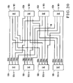
- a conventional 4-input/4-output switch (4 x 4 switch) includes eight Single-Pole 4-Throw (SP4T) switches 103 1 to 103 8 in correspondence with input terminals 101 1 to 101 4 and output terminals 102 1 to 102 4 .
- the SP4T switches 103 1 to 103 8 are bidirectional switches, each functioning both as a 1-input/4-output switch and a 4-input/1-output switch.
- Each of the SP4T switches 103 1 to 103 8 includes one common terminal and four individual terminals. Sixteen interconnection transmission lines 104 11 to 104 44 connect the individual terminals of the SP4T switches 103 1 to 103 4 on the input side to the individual terminals of the SP4T switches 103 5 to 103 8 on the output side. Each of the SP4T switches 103 1 to 103 8 is designed such that the common terminal connects to one of the four individual terminals (does not connect to the remaining three terminals). These switches are controlled as a whole such that the four input terminals 101 1 to 101 4 one-to-one connect to the four output terminals 102 1 to 102 4 . Referring to Fig. 20, the symbol "O" with a satin-like pattern indicates an interconnection intersection 116 where two transmission lines intersect each other but do not electrically connect to each other.
- the first problem is that it is difficult to achieve low insertion loss and high isolation while reducing the circuit size. This problem originates from the necessity to make the interconnection transmission lines 104 11 to 104 44 have finite lengths and not a little increase in insertion loss caused by the finite lengths.
- the transmission lines 104 11 to 104 44 comprise, for example, coplanar waveguides
- a matrix switch is required to have a high isolation characteristic between the respective paths.
- the isolation between coplanar waveguides increases as the ground conductor width between the lines increases.
- each connection path inevitably becomes long. This greatly cancels out the above reducing effect of insertion loss.
- connection paths amounts to an increase in circuit size.
- this increase in circuit size causes an increase in cost.
- n be the numbers of input terminals 101 1 to 101 n and output terminals 102 1 to 102 n , the required number of connection paths is the square of n. Therefore, the larger the switch size, the more conspicuous these problems become. This poses a serious problem in the matrix switch with a size of 4 x 4 or more shown in Fig. 20.
- the second problem is that as the numbers of input terminals 101 1 to 101 n and output terminals 102 1 to 102 n increase, the number of connection path intersections increases, and the isolation characteristic deteriorates.
- the 4 x 4 switch shown in Fig. 20 there are as many as 36 interconnection intersections.
- the number of interconnection intersections in an 8 x 8 switch reaches as many as 784.
- the larger the size of a matrix switch the larger the number of interconnection intersections becomes, resulting in a deterioration in isolation characteristic.
- the third problem is that an increase in the number of switch control lines will cause a deterioration in isolation characteristic.
- This problem originates from the necessity to provide switches on both the input and output sides. If SPnT switches each functioning both as a 1-input/n-output switch and an n-input/1-output switch require n control lines each, a 4 x 4 switch requires 32 control lines, and an 8 x 8 switch requires as many as 128 control lines. These control lines inevitably intersect the interconnection transmission lines 104 11 to 104 44 . This leads to a deterioration in isolation characteristic.
- n 1-input/n-output switches and n n-input/1-output switches are respectively arranged on both the input and output sides. That is, the problems originate from the necessity of n 2 interconnection transmission lines for connecting these switches.
- This conventional matrix switch operates even if the switches on either the input side or the output side are removed. For example, even if the SP4T switches 103 5 to 103 8 on the output side in Fig. 20 are removed, the resultant structure operates as a 4 x 4 switch. In this case, however, transmission lines coupled to the OFF terminals of the SP4T switches 103 1 to 103 4 on the input side become open stubs when viewed from the output terminals 102 1 to 102 4 . An OFF terminal is an individual terminal which does not connect to a common terminal. An open stub is a portion which branches off from a main transmission line and has an open end.
- a 4 x 4 switch has three open stubs for each output terminal, and an 8 x 8 switch has seven open stubs for each output terminal.
- Open stubs increase capacitance. As a result, return loss increases with an increase in frequency. This makes it difficult to perform broadband operation at several GHz or more.
- the length of an open stub almost corresponds to the interval between an input-side switch and an output-side switch. As the interval between two switches, a 4 x 4 switch requires a length corresponding to a space where at least 16 interconnection transmission lines are arranged, and an 8 x 8 switch requires a space where 64 interconnection transmission lines are arranged.
- the length of an open stub can therefore decrease as the width of a transmission line and a transmission line interval decrease. However, consideration must be given to the tradeoff with insertion loss and isolation characteristic.
- the capacitance caused by an open stub can also be reduced by increasing the characteristic impedance of an interconnection transmission line.
- the interval between the central conductor and the ground conductor must be increased. This leads to an increase in the length of an interconnection transmission line which becomes an open stub, and greatly cancels out the characteristic impedance increasing effect.
- a matrix switch is characterized by comprising n (n is an even number not less than 2) 1 x n switches which are grouped in twos to form switch pairs, first conductive lines arranged in ns for each switch pair, n second conductive lines which respectively connect to different lines of the first conductive lines which are respectively arranged on the switch pairs, a dielectric layer on which the first conductive lines and the second conductive lines are separately arranged on not less than two layers, and a ground conductor which forms a transmission line together with at least one of the first conductive line and the second conductive line and the dielectric layer, wherein the 1 x n switch comprises one common terminal and n individual terminals arranged on a side different from that of the common terminal, two 1 x n switches forming the switch pair are arranged such that individual terminals of the 1 x n switches are spaced apart from each other to face each other, and the first conductive lines connect the respective individual terminals of the two 1 x n switches to
- the number of conductive lines existing between two 1 x n switches forming a switch pair can decrease from n 2 in the prior art to n.
- the space where the conductive lines are arranged decreases. Since a required 1 x n switch reduces to 1/2 that in the prior art, the matrix switch can be reduced in size. A reduction in size can achieve a reduction in cost.
- the isolation characteristic improves.
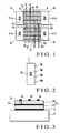
- a matrix switch according to the first embodiment of the present invention is a 4 x 4 switch including four input terminals (first terminals) 1 1 to 1 4 , four output terminals (second terminals) 2 1 to 2 4 , and four SP4T switches 3 1 to 3 4 .
- Each of the SP4T switches 3 1 to 3 4 is a 1 x 4 switch including one common terminal 3a and four individual terminals 3b 1 to 3b 4 like a SP4T switch 3 shown in Fig. 2.
- the common terminal 3a and the individual terminals 3b 1 to 3b 4 are arranged on opposite sides of the switch.
- Each of the SP4T switches 3 1 to 3 4 is controlled such that the common terminal 3a of the self-switch selectively connects to one of the individual terminals 3b 1 to 3b 4 while not connecting to the remaining three terminals.
- each of the SP4T switches 3 1 to 3 4 outputs a signal input from the common terminal 3a to one of the individual terminals 3b 1 to 3b 4 , and outputs a signal input from one of the individual terminals 3b 1 to 3b 4 to the common terminal 3a.
- Each of the SP4T switches 3 1 to 3 4 is a bidirectional switch functioning both as a 1-input/4-output switch and a 4-input/1-output switch. Note that it suffices if the common terminal 3a and the individual terminals 3b 1 to 3b 4 are arranged on different sides of the switch. That is, the terminals 3a and 3b 1 to 3b 4 may be arranged on adjacent sides of the switch.
- the four SP4T switches 3 1 to 3 4 are grouped in twos to form two switch pairs. More specifically, the SP4T switches 3 1 and 3 4 constitute the first switch pair, and the SP4T switches 3 2 and 3 3 constitute the second switch pair.
- the SP4T switches 3 1 and 3 4 constituting the first switch pair are arranged such that the individual terminals 3b 1 to 3b 4 of one switch face those of the other switch.
- the SP4T switches 3 2 and 3 3 constituting the second switch pair are arranged in the same manner.
- the four individual terminals 3b 1 to 3b 4 of the SP4T switch 3 1 connect to the four individual terminals 3b 1 to 3b 4 of the SP4T switch 3 4 via four first conductive lines 4 11 to 4 14 .
- the four individual terminals 3b 1 to 3b 4 of the SP4T switch 3 2 connect to the four individual terminals 3b 1 to 3b 4 of the SP4T switch 3 3 via four first conductive lines 4 21 to 4 24 .
- the first conductive lines 4 11 to 4 14 and 4 21 to 4 24 are arranged parallel to each other.
- the first conductive lines 4 11 to 4 14 respectively connect to the first conductive lines 4 21 to 4 24 via second conductive lines 5 1 to 5 4 . More specifically, the first conductive lines 4 11 and 4 21 connect to each other via the second conductive line 5 1 ; the first conductive lines 4 12 and 4 22 , via the second conductive line 5 2 ; the first conductive lines 4 13 and 4 23 , via the second conductive line 5 3 ; and the first conductive lines 4 14 and 4 24 , via the second conductive line 5 4 .
- the second conductive lines 5 1 to 5 4 are arranged parallel to each other in a direction to intersect the first conductive lines 4 11 to 4 14 and 4 21 to 4 24 (a direction perpendicular to them in Fig. 1).
- the input terminals 1 1 to 1 4 to which signals are input connect to the common terminals 3a of the SP4T switches 3 1 to 3 4 . End portions of the second conductive lines 5 1 to 5 4 are extracted outside the area where the conductive lines 4 11 to 4 14 and 4 21 to 4 24 are arranged and connect to the output terminals 2 1 to 2 4 from which signals are output.
- the SP4T switches 3 1 to 3 4 are controlled as a whole such that the four input terminals 1 1 to 1 4 one-to-one connect to the four output terminals 2 1 to 2 4 .
- the first conductive lines 4 11 to 4 14 and 4 21 to 4 24 and the second conductive lines 5 1 to 5 4 constitute microstrip lines (transmission lines) together with a ground conductor 6 formed on a substrate 9 and a dielectric layer 8 formed on the ground conductor 6.
- the dielectric layer 8 has a two-layer structure comprising a first dielectric layer 8 1 and a second dielectric layer 8 2 .
- the first dielectric layer 8 1 is stacked on the ground conductor 6, and the second dielectric layer 8 2 is stacked on the first dielectric layer 8 1 .
- the first conductive lines 4 11 to 4 14 and 4 21 to 4 24 are arranged on the first dielectric layer 8 1
- the second conductive lines 5 1 to 5 4 are arranged on the second dielectric layer 8 2 .
- the first conductive lines 4 11 to 4 14 and 4 21 to 4 24 connect to the second conductive lines 5 1 to 5 4 at connecting portions 15 indicated by " ⁇ " in Fig. 1 via through holes 7 1 formed in the second dielectric layer 8 2 .
- FIG. 3 is a view for explaining a state wherein two conductive lines connect to each other via a dielectric layer, with an illustration of the second conductive line 5 4 being omitted.
- the above arrangement makes it possible to decrease the number of conductive lines existing between the opposite switches of the respective switch pairs from 16 in the prior art shown in Fig. 20 to 4 (the second conductive lines 5 1 to 5 4 ). If, therefore, conductive lines with the same line width and the same line interval are used, the interval between the SP4T switches 3 1 and 3 4 and between the SP4T switches 3 2 and 3 3 of the first and second switch pairs can decrease to about 1/4 that in the prior art.
- each of the SP4T switches 3 1 to 3 4 the first conductive lines coupled to the OFF terminals become open stubs, together with some of the second conductive lines in some cases. Therefore, the switching operation, three open stubs exist for each of the output terminals 2 1 to 2 4 .
- decreasing the interval between the SP4T switches 3 1 and 3 4 and between the SP4T switches 3 2 and 3 3 makes it possible to decrease the length of each open stub to about 1/12 that in the prior art. This allows broadband operation in a bandwidth 10 times or more as wide as that in the arrangement of the prior art in which the SP4T switches 103 5 to 103 8 on the output side are removed.
- the length of the transmission lines between input terminals and output terminals in the ON state decreases, insertion loss can be reduced while the path dependency of insertion loss can be reduced.
- the number of interconnection intersections can decrease from 36 in the prior art shown in Fig. 20 to 14, and an improvement in isolation characteristic can be attained.
- the ground conductor 6 and the dielectric layers 8 1 and 8 2 are sequentially formed on the substrate 9, with the dielectric layers 8 1 and 8 2 having a thickness of several ⁇ m to several ten ⁇ m.
- This structure makes it possible to maintain high inter-line isolation even if the line interval is decreased as compared with microstrip lines using a substrate lower surface ground and coplanar waveguides formed on a substrate upper surface. Therefore, a switch with a broader bandwidth can be implemented.
- the above structure can increase a characteristic impedance with a narrow line interval as compared with coplanar waveguides, and hence makes it easy to reduce the capacitance caused by an open stub, thereby improving return loss.
- the matrix switch shown in Figs. 4 and 5 is a modification of the matrix switch shown in Figs. 1 and 3.
- the second conductive lines 5 1 to 5 4 are arranged on the first dielectric layer 8 1
- the first conductive lines 4 11 to 4 14 and 4 21 to 4 24 are arranged on the second dielectric layer 8 2 .
- This arrangement can obtain the same effects as those of the matrix switch shown in Figs. 1 and 3.
- Note that an illustration of the second conductive line 5 4 is omitted in Fig. 5 as well for the same reason as that for Fig. 3.
- the conductive line width on the first dielectric layer 8 1 is preferably smaller than that on the second dielectric layer 8 2 . This makes it possible to reduce the characteristic impedance difference between the conductive lines on the first dielectric layer 8 1 and the conductive lines on the second dielectric layer 8 2 . Both the characteristic impedances can be equalized. This makes it possible to improve the characteristics of the switch.
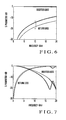
- a 4 x 4 switch with a bandwidth of about 20 GHz could be implemented by setting the line widths of the first conductive lines 4 11 to 4 14 and 4 21 to 4 24 and the second conductive lines 5 1 to 5 4 to about 5 to 10 ⁇ m, the thicknesses of the lines to about 1 to 5 ⁇ m, and the thicknesses of the first and second dielectric layers 8 1 and 8 2 to about 2 to 5 ⁇ m (dielectric constant: about 3).
- Fig. 6 shows the simulation result obtained from a 4 x 4 switch designed with the above dimensions.
- Fig. 7 shows the simulation result obtained from a 4 x 4 switch with a conventional arrangement.
- a 4 x 4 switch with a conventional arrangement is assumed to be the switch obtained by removing the output-side SP4T switches 103 5 to 103 8 of the matrix switch shown in Fig. 20, and connecting end portions of the interconnection transmission lines 104 11 to 104 14 , 104 21 to 104 24 , 104 31 to 104 34 , and 104 41 to 104 44 to which the individual terminals of the SP4T switches 103 5 to 103 8 have connected.
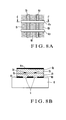
- the matrix switch shown in Figs. 8A and 8B is a modification of the matrix switch shown in Figs. 4 and 5.
- gaps G are formed in a ground conductor 6 immediately below second conductive lines 5 1 to 5 4 arranged on a first dielectric layer 8 1 . This reduces the capacitances of the second conductive lines 5 1 to 5 4 , and hence can increase the characteristic impedance without decreasing the line width of the second conductive lines 5 1 to 5 4 .
- the line width of the second conductive lines 5 1 to 5 4 on the first dielectric layer 8 1 is set to be almost equal to that of first conductive lines 4 11 to 4 14 and 4 21 to 4 24 on a second dielectric layer 8 2 , and the widths of the gaps G in the ground conductor 6 are set such that the characteristic impedance of the second conductive lines 5 1 to 5 4 becomes equal to that of the first conductive lines 4 11 to 4 14 and 4 21 to 4 24 .
- ground conductors 6 1 , 6 2 , and 6 3 are ground conductors which connect to the same potential.
- the matrix switch shown in Figs. 9A and 9B is another modification of the matrix switch shown in Figs. 4 and 5.
- the gaps G are formed in the ground conductor 6 immediately below the first and second conductive lines 4 11 to 4 14 , 4 21 to 4 24 , and 5 1 to 5 4 except for intersection areas between the second conductive lines 5 1 to 5 4 arranged on the first dielectric layer 8 1 and the first conductive lines 4 11 to 4 14 and 4 21 to 4 24 arranged on the second dielectric layer 8 2 .
- This arrangement can further increase the characteristic impedances.
- the line width of the second conductive lines 5 1 to 5 4 on the first dielectric layer 8 1 is smaller than that of the first conductive lines 4 11 to 4 14 and 4 21 to 4 24 on the second dielectric layer 8 2 , and the widths of the gaps G in the ground conductor 6 are set such that the characteristic impedance of the second conductive lines 5 1 to 5 4 becomes equal to that of the first conductive lines 4 11 to 4 14 and 4 21 to 4 24 .
- This arrangement can greatly reduce the capacitance caused by open stubs by increasing the characteristic impedances. As a consequence, the return loss can be improved, and hence a matrix switch with a broader bandwidth can be implemented.
- this embodiment can also be applied to a case wherein the first conductive lines 4 11 to 4 14 and 4 21 to 4 24 are arranged on the first dielectric layer 8 1 , and the second conductive lines 5 1 to 5 4 are arranged on the second dielectric layer 8 2 .
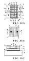
- the matrix switch shown in Figs. 10A to 10C is a modification of the matrix switch shown in Figs. 1 and 3.
- output terminals 2 1 to 2 4 are gathered on one side of the matrix switch.
- first and second conductive lines 4 11 to 4 14 , 4 21 to 4 24 , and 5 1 to 5 4 are formed on a second dielectric layer 8 2 in orthogonal directions. Note that portions of the first conductive lines 4 11 to 4 14 and 4 21 to 4 24 (only a conductive line 4 21 ' is shown in Figs.
- first dielectric layer 8 1 is formed on a first dielectric layer 8 1 at intersects 16 between the first conductive lines 4 11 to 4 14 and 4 21 to 4 24 and the second conductive lines 5 1 to 5 4 except for the connecting portions.
- These portions of the first conductive lines 4 11 to 4 14 and 4 21 to 4 24 connect to the remaining portions of the first conductive lines 4 11 to 4 14 and 4 21 to 4 24 on the second dielectric layer 8 2 via through holes 7 1 and 7 2 and the like formed in the second dielectric layer 8 2 .
- reference numeral "16" denoting an intersection is attached to only one portion in Fig. 10A, all the symbols " ⁇ " with satin-like patterns indicate intersections 16. This applies to Figs. 13A and 15 to be described later.
- portions of the second conductive lines 5 1 to 5 4 may be formed on the first dielectric layer 8 1 at the intersections 16 and connect to the remaining portions on the second dielectric layer 8 2 via through holes.
- the conductive line width on the first dielectric layer 8 1 is preferably smaller than that on the second dielectric layer 8 2 . This can decrease the characteristic impedance difference between the conductive lines on the first dielectric layer 8 1 and the conductive lines on the second dielectric layer 8 2 , and hence can improve the characteristics of the matrix switch. In addition, gathering the output terminals 2 1 to 2 4 on one side of the matrix switch makes it easy to extract input and output terminals in opposite directions, as shown in Fig. 13.
- the matrix switch shown in Figs. 11A to 11C is a modification of the matrix switch shown in Figs. 10A to 10C.
- gaps G are formed in a ground conductor 6 immediately below a conductive line 4 21 ' and the like on the first dielectric layer 8 1 . This reduces the capacitances of the transmission lines, and hence can increase characteristic impedances without decreasing the line widths of a conductive line 4 21 ' and the like.
- the conductive line width on the first dielectric layer 8 1 is set to be almost equal to that on the second dielectric layer 8 2 , and the widths of the gaps G are set such that the characteristic impedance of the conductive lines on the first dielectric layer 8 1 becomes equal to that of the conductive lines on the second dielectric layer 8 2 . This makes it possible to further reduce the insertion loss of the matrix switch.
- the matrix switch shown in Figs. 12A to 12C is a modification of the matrix switch shown in Figs. 10A to 10C.
- the gaps G are formed in the ground conductor 6 on a substrate 9 at the intersections between the first conductive lines 4 11 to 4 14 and 4 21 to 4 24 and the second conductive lines 5 1 to 5 4 except for the connecting portions.
- Portions of the first conductive lines 4 11 to 4 14 and 4 21 to 4 24 are formed in the areas on the substrate 9 in which the gaps G are formed (below the first dielectric layer 8 1 ).
- first conductive lines 4 11 to 4 14 and 4 21 to 4 24 connect to the remaining portions of the first conductive lines 4 11 to 4 14 and 4 21 to 4 24 on the second dielectric layer 8 2 via the through holes 7 1 and 7 2 formed in the first and second dielectric layers 8 1 and 8 2 .
- Conductors 6' are formed on the first dielectric layer 8 1 immediately below the above intersections. The conductors 6' connect to the ground conductor 6 on the substrate 9 via through holes 7 3 and 7 4 and the like formed in the first dielectric layer 8 1 .
- portions of the second conductive lines 5 1 to 5 4 may be formed in the areas where the gaps G are formed, and connect to the remaining portions on the second dielectric layer 8 2 via through holes.
- This embodiment is not limited to the above arrangement, and may be configured to extract the output terminals 2 1 , 2 2 , 2 3 , and 2 4 from different sides as in the embodiment shown in Fig. 1.
- the gaps G may be formed in the ground conductor 6 immediately below the conductive lines on the second dielectric layer 8 2 .
- a matrix switch according to the fourth embodiment of the present invention is equivalent to the matrix switch shown in Fig. 10 except that SP4T switches 3 1 to 3 4 comprise field-effect transistors (FETs) 10 11 to 10 14 , 10 21 to 10 24 , 10 31 to 10 34 , and 10 41 to 10 44 , and resistors 11 11 to 11 14 , 11 21 to 11 24 , 11 31 to 11 34 , and 11 41 to 11 44 .
- FETs field-effect transistors
- One of the drain and source electrodes of each of the FETs 10 11 to 10 14 connects to the common terminal of the SP4T switch, and the other of the drain and source electrodes of each FET connects to an individual terminal of the SP4T switch.
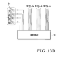
- the gate electrodes of the FETs 10 11 to 10 14 connect to a controller 14 via the resistors 11 11 to 11 14 , as shown in Fig. 13B.
- Such an FET switch arrangement makes it possible to implement high-speed switching with zero power consumption, and to use a matrix switch by exchanging input and output terminals.
- the controller 14 controls the SP4T switches 3 1 to 3 4 in the above manner. That is, the controller 14 controls each of the SP4T switches 3 1 to 3 4 such that the common terminal connects to only one of the four individual terminals.
- V H is applied to one of the resistors 11 11 to 11 14
- V L is applied to the remaining three resistors.
- the matrix switch is controlled as a whole such that four input terminals 1 1 to 1 4 one-to-one connect to four output terminals 2 1 to 2 4 .
- the input terminals 1 1 to 1 4 and the output terminals 2 1 to 2 4 are arranged on different sides through the area where first conductive lines 4 11 to 4 14 and 4 21 to 4 24 and second conductive lines 5 1 to 5 4 are arranged.
- Conductive lines (third conductive lines) 12 11 to 12 14 of input transmission lines are interposed between the common terminals and the input terminals 1 1 to 1 4 of the SP4T switches 3 1 to 3 4 .
- Conductive lines (fourth conductive lines) 12 21 to 12 24 of output transmission lines are interposed between end portions and the output terminals 2 1 to 2 4 of the second conductive lines 5 1 to 5 4 .
- bending the third conductive lines 12 11 to 12 14 from the common terminals to the opposite side to the output terminals 2 1 to 2 4 makes it possible to gather the input terminals 1 1 to 1 4 on the opposite side to the output terminals 2 1 to 2 4 .
- the third and fourth conductive lines 12 11 to 12 14 and 12 21 to 12 24 are arranged on the second dielectric layer 8 2 in Figs. 11B and 11C to form microstrip lines by using the ground conductor 6 and a common ground conductor inside the matrix switch.
- the third and fourth conductive lines 12 11 to 12 14 and 12 21 to 12 24 are not required to increase characteristic impedances unlike the first and second conductive lines 4 11 to 4 14 and 4 21 to 4 24 and 5 1 to 5 4 for interconnections. This makes it possible to increase the line widths as compared with the first and second conductive lines 4 11 to 4 14 and 4 21 to 4 24 and 5 1 to 5 4 so as to match an input/output of 50 O.
- first and second conductive lines 4 11 to 4 14 , 4 21 to 4 24 , and 5 1 to 5 4 may have the cross-sectional structures shown in Figs. 3, 5, 8B, 9B, 11B, 11C, 12B, and 12C.
- a matrix switch according to the fifth embodiment of the present invention is an application of the 4 x 4 switch shown in Figs. 1 and 3 to an 8 x 8 switch. As shown in Fig. 14, this matrix switch includes eight input terminals (first terminals) 1 1 to 1 8 , eight output terminals (second terminals) 2 1 to 2 8 , and eight SP8T switches 13 1 to 13 8 .
- the SP8T switches 13 1 to 13 8 each are a 1 x 8 switch including one common terminal and eight individual terminals.
- the eight SP8T switches 13 1 to 13 8 are grouped in twos to form four switch pairs. More specifically, the SP8T switches 13 1 and 13 8 constitute the first switch pair; the SP8T switches 13 2 and 13 7 , the second switch pair; the SP8T switches 13 3 and 13 6 , the third switch pair; and the SP8T switches 13 4 and 13 5 , the fourth switch pair.
- the SP8T switches 13 1 and 13 8 constitute the first switch pair are spaced apart from each other such that their individual terminals face each other.
- the SP8T switches 13 2 and 13 7 , 13 3 and 13 6 , and 13 4 and 13 5 constituting the remaining switch pairs are arranged in the same manner.
- the eight individual terminals of the SP8T switch 13 1 connect to the eight individual terminals of the SP8T switch 13 8 via eight first conductive lines 4 11 to 4 18 .
- the eight individual terminals of the SP8T switch 13 2 connect to the eight individual terminals of the SP8T switch 13 7 via eight first conductive lines 4 21 to 4 28 .
- the eight individual terminals of the SP8T switch 13 3 connect to the eight individual terminals of the SP8T switch 13 6 via eight first conductive lines 4 31 to 4 38 .
- the eight individual terminals of the SP8T switch 13 4 connect to the eight individual terminals of the SP8T switch 13 5 via eight first conductive lines 4 41 to 4 48 .
- the first conductive lines 4 11 to 4 18 , 4 21 to 4 28 , 4 31 to 4 38 , and 4 41 to 4 48 are arranged parallel to each other.
- the first conductive lines 4 11 , 4 21 , 4 31 , and 4 41 connect to each other via the second conductive line 5 1 ; the first conductive lines 4 12 , 4 22 , 4 32 , and 4 42 , via the second conductive line 5 2 ; the first conductive lines 4 13 , 4 23 , 4 33 , and 4 43 , via the second conductive line 5 3 ; the first conductive lines 4 14 , 4 24 , 4 34 , and 4 44 , via the second conductive line 5 4 ; the first conductive lines 4 15 , 4 25 , 4 35 , and 4 45 , via the second conductive line 5 5 ; the first conductive lines 4 16 , 4 26 , 4 36 , and 4 46 , via the second conductive line 5 6 ; the first conductive lines 4 17 , 4 27 , 4 37 , and 4 47 , via the second conductive line 5 7 ; and the first conductive lines 4 18 , 4 28 , 4 38 , and 4 48 , via the second conductive
- the second conductive lines 5 1 to 5 8 are arranged parallel to each other in a direction to cross (in Fig. 14, a direction perpendicular to) the first conductive lines 4 11 to 4 18 , 4 21 to 4 28 , 4 31 to 4 38 , and 4 41 to 4 48 .
- the input terminals 1 1 to 1 8 respectively connect to the common terminals of the SP8T switches 13 1 to 13 8 . End portions of the second conductive lines 5 1 to 5 8 are extracted outside the area where the conductive lines 4 11 to 4 18 , 4 21 to 4 28 , 4 31 to 4 38 , and 4 41 to 4 48 are arranged and connect to output terminals 2 1 to 2 8 .
- the SP8T switches 13 1 to 13 8 are controlled as a whole such that the eight input terminals 1 1 to 1 8 one-to-one connect to the eight output terminals 2 1 to 2 8 .
- the first conductive lines 4 11 to 4 18 , 4 21 to 4 28 , 4 31 to 4 38 , and 4 41 to 4 48 and the second conductive lines 5 1 to 5 8 constitute microstrip lines together with a ground conductor 6 formed on a substrate 9 and a first dielectric layer 8 1 and a second dielectric layer 8 2 sequentially formed on the ground conductor 6.
- the first conductive lines 4 11 to 4 18 , 4 21 to 4 28 , 4 31 to 4 38 , and 4 41 to 4 48 are arranged on the first dielectric layer 8 1
- the second conductive lines 5 1 to 5 8 are arranged on the second dielectric layer 8 2 .
- the first conductive lines 4 11 to 4 18 , 4 21 to 4 28 , 4 31 to 4 38 , and 4 41 to 4 48 and the second conductive lines 5 1 to 5 8 connect to each other via through holes 7 1 formed in the second dielectric layer 8 2 at connecting portions 15 indicated by " ⁇ " in Fig. 14.
- the length of the transmission line between input and output terminals in the ON state decreases, insertion loss can be reduced, and the path dependency of insertion loss can be reduced.
- the ground conductor 6 and the dielectric layers 8 1 and 8 2 are sequentially formed on the substrate 9, and the thicknesses of the dielectric layers 8 1 and 8 2 are set to several ⁇ m to several ten ⁇ m.
- This structure makes it possible to maintain high inter-line isolation even if the line interval is decreased as compared with microstrip lines using a substrate lower surface ground and coplanar waveguides formed on a substrate upper surface. Therefore, a switch with a broader bandwidth can be implemented.
- the above structure can increase a characteristic impedance with a narrow line interval as compared with coplanar waveguides, and hence makes it easy to reduce the capacitance caused by an open stub, thereby improving return loss.
- an 8 x 8 switch with a bandwidth of about 10 GHz could be implemented by setting the line widths of the first conductive lines 4 11 to 4 18 , 4 21 to 4 28 , 4 31 to 4 38 , and 4 41 to 4 48 and the second conductive lines 5 1 to 5 8 to about 5 to 10 ⁇ m, the thicknesses of the lines to about 1 to 5 ⁇ m, and the thicknesses of the first and second dielectric layers 8 1 and 8 2 to about 2 to 5 ⁇ m (dielectric constant: about 3).
- this embodiment is not limited to the arrangement shown in Fig. 14, and the second conductive lines 5 1 to 5 8 may be formed on the first dielectric layer 8 1 , and the first conductive lines 4 11 to 4 18 , 4 21 to 4 28 , 4 31 to 4 38 , and 4 41 to 4 48 may be formed on the second dielectric layer 8 2 as in the 4 x 4 switch shown in Figs. 4 and 5. As shown in Figs. 8B and 9B, the gaps G may be formed in the ground conductor 6.
- the matrix switch shown in Fig. 15 is a modification of the matrix switch shown in Fig. 14. According to this matrix switch, output terminals 2 1 to 2 8 are gathered on one side of the matrix switch.
- the first and second conductive lines 4 11 to 4 18 , 4 21 to 4 28 , 4 31 to 4 38 , 4 41 to 4 48 , and 5 1 to 5 8 are formed on a second dielectric layer 8 2 in orthogonal directions.
- portions of the first conductive lines 4 11 to 4 18 , 4 21 to 4 28 , 4 31 to 4 38 , and 4 41 to 4 48 are formed on a first dielectric layer 8 1 at intersections 16 of the first conductive lines 4 11 to 4 18 , 4 21 to 4 28 , 4 31 to 4 38 , and 4 41 to 4 48 and the second conductive lines 5 1 to 5 8 except for the connecting portions. These portions connect to the remaining portions of the first conductive lines 4 11 to 4 18 , 4 21 to 4 28 , 4 31 to 4 38 . and 4 41 to 4 48 on the second dielectric layer 8 2 via through holes 7 1 and 7 2 formed in the second dielectric layer 8 2 .
- portions of the second conductive lines 5 1 to 5 8 may be formed on the first dielectric layer 8 1 at the intersections 16 and connect to the remaining portions on the second dielectric layer 8 2 via through holes.
- the conductive line width on the first dielectric layer 8 1 is preferably smaller than that on the second dielectric layer 8 2 . This makes it possible to reduce the characteristic impedance difference between the conductive lines on the first dielectric layer 8 1 and the conductive lines on the second dielectric layer 8 2 and improve the characteristics of the matrix switch. In addition, gathering the output terminals 2 1 to 2 8 on one side of the matrix switch facilitates extraction of input and output terminals in opposite directions.
- the gaps G may be formed in a ground conductor 6 immediately below portions (e.g., a conductive line 4 21 ') of the conductive lines on the first dielectric layer 8 1 .
- conductors 6' may be formed below the intersections 16 of the first conductive lines 4 11 to 4 18 , 4 21 to 4 28 , 4 31 to 4 38 , and 4 41 to 4 48 and the second conductive lines 5 1 to 5 8 and connect to the ground conductor 6 on a substrate 9 via through holes 7 3 and 7 4 .
- each SP8T switch may comprise eight FETs.
- the SP4T switches 3 1 to 3 4 and SP8T switches 13 1 to 13 8 in the above embodiments may comprise micro-mechanical switches (MEMS (Micro-Electro-Mechanical Systems) switches) instead of FETs.
- MEMS Micro-Electro-Mechanical Systems
- Using MEMSs increases the control voltage and prolongs the switching time as compared with a case wherein FETs are used, but can achieve the low insertion loss and high isolation of switches.
- part or all of the above matrix switch is preferably integrated on a semiconductor substrate. That is, a semiconductor substrate is preferably used as a substrate 9.
- the present invention can use a dielectric layer with a single-layer structure or a dielectric layer with a multi-layer structure comprising three or more layers.
- first and second conductive lines are arranged on the dielectric layer and the substrate 9 immediately below the dielectric layer.
- first and second conductive lines may be separately arranged on the three or more layers.
- first conductive lines 4 11 to 4 14 and 4 21 to 4 24 and the second conductive lines 5 1 to 5 4 constitute microstrip lines together with the dielectric layer 8 and the ground conductor 6.
- first conductive lines 4 11 to 4 14 and 4 21 to 4 24 or the second conductive lines 5 1 to 5 4 may constitute coplanar waveguides together with a ground conductor formed in the same plane.
- the input terminals 1 1 to 1 4 and the output terminals 2 1 to 2 4 may be exchanged. That is, the output terminals 2 1 to 2 4 may be used as input terminals, and the input terminals 1 1 to 1 4 may be used as output terminals.
- Fig. 16 shows the arrangement obtained by exchanging the input terminals 1 1 to 1 4 and the output terminals 2 1 to 2 4 in the matrix switch shown in Fig. 1. In this case, the output terminals 2 1 to 2 4 become the first terminals, and the input terminals 1 1 to 1 4 become the second terminals.
- the input terminals 1 1 to 1 8 and the output terminals 2 1 to 2 8 may be exchanged.
- n x n switch includes n SPnT switches (1 x n switches) grouped in twos to form switch pairs, first conductive lines arranged in ns for each switch pair, and n second conductive lines.
- a 2 x 2 switch includes two SPDT switches 23 1 and 23 2 , two first conductive lines 4 11 and 4 12 , and two second conductive lines 5 1 and 5 2 .
- output terminals 2 1 and 2 2 are arranged on opposite sides of the area where first and second conductive lines 4 11 , 4 12 , 5 1 , and 5 2 are arranged.
- output terminals 2 1 and 2 2 are arranged on the same side.
- a 16 x 16 switch includes 16 SP16T switches 33 1 to 33 16 constituting eight switch pairs, first conductive lines 4 arranged in 16s for each switch pair, and 16 second conductive lines 5.
- the above SPnT switch is a switch which functions as both a 1-input/n-output switch and an n-input/1-output switch.
- the present invention can use a switch having no bidirectionality instead of such an SPnT switch. More specifically, a matrix switch like that shown in Fig. 1 can use 1-input/n-output switches, and a matrix switch like that shown in Fig. 16 can use n-input/1-output switches.
- the matrix switch according to the present invention can be used for a 10 GbE router, network switch, high-speed video signal switcher, optical cross-connect, protection switch, and the like.
Landscapes
- Electronic Switches (AREA)
- Waveguide Switches, Polarizers, And Phase Shifters (AREA)
Abstract
Description
- The present invention relates to a matrix switch which outputs a signal from an arbitrary input terminal to an arbitrary output terminal by switching signal paths between a plurality of input terminals and a plurality of output terminals and, more particularly, to a matrix switch including a plurality of 1 x n switches (n is an even number equal to or more than 2).
- A multi-input/multi-output matrix switch is used to, for example, switch signal paths at nodes in a network. A conventional n-input/n-output switch comprises n 1-input/n-output switches, n n-input/1-output switches, and n2 connection means for connecting the switches to each other. Reference 1 (
Japanese Patent Laid-Open No. 9-9312 reference 1 has an arrangement which can be applied as a cross-connect switch which can output input signals from n input terminals 1011 to 101n in all combinations to n output terminals 1021 to 102n, as shown in Fig. 19. This arrangement will be described in more detail below by exemplifying the case of n = 4. - As shown in Fig. 20, a conventional 4-input/4-output switch (4 x 4 switch) includes eight Single-Pole 4-Throw (SP4T) switches 1031 to 1038 in correspondence with input terminals 1011 to 1014 and output terminals 1021 to 1024. The SP4T switches 1031 to 1038 are bidirectional switches, each functioning both as a 1-input/4-output switch and a 4-input/1-output switch.
- Each of the SP4T switches 1031 to 1038 includes one common terminal and four individual terminals. Sixteen interconnection transmission lines 10411 to 10444 connect the individual terminals of the SP4T switches 1031 to 1034 on the input side to the individual terminals of the SP4T switches 1035 to 1038 on the output side. Each of the SP4T switches 1031 to 1038 is designed such that the common terminal connects to one of the four individual terminals (does not connect to the remaining three terminals). These switches are controlled as a whole such that the four input terminals 1011 to 1014 one-to-one connect to the four output terminals 1021 to 1024. Referring to Fig. 20, the symbol "O" with a satin-like pattern indicates an
interconnection intersection 116 where two transmission lines intersect each other but do not electrically connect to each other. - The following problems arise in the conventional matrix switch.
- The first problem is that it is difficult to achieve low insertion loss and high isolation while reducing the circuit size. This problem originates from the necessity to make the interconnection transmission lines 10411 to 10444 have finite lengths and not a little increase in insertion loss caused by the finite lengths. When the transmission lines 10411 to 10444 comprise, for example, coplanar waveguides, in order to reduce insertion loss, it is necessary to increase the central conductor width and the gap between the central conductor and the ground conductor. This is because the characteristic impedance of a coplanar waveguide is almost uniquely determined by the central conductor width and the above gap.
- On the other hand, a matrix switch is required to have a high isolation characteristic between the respective paths. In this case, the isolation between coplanar waveguides increases as the ground conductor width between the lines increases. In order to attain characteristics with a low insertion loss and high isolation, it is necessary to increase both the central conductor width and the ground conductor width. However, in a matrix switch in which transmission lines are arranged at a high density, each connection path inevitably becomes long. This greatly cancels out the above reducing effect of insertion loss.
- An increase in the length of connection paths amounts to an increase in circuit size. When a matrix switch is to be integrated on a semiconductor substrate, in particular, this increase in circuit size causes an increase in cost. Letting n be the numbers of input terminals 1011 to 101n and output terminals 1021 to 102n, the required number of connection paths is the square of n. Therefore, the larger the switch size, the more conspicuous these problems become. This poses a serious problem in the matrix switch with a size of 4 x 4 or more shown in Fig. 20.
- The second problem is that as the numbers of input terminals 1011 to 101n and output terminals 1021 to 102n increase, the number of connection path intersections increases, and the isolation characteristic deteriorates. In the 4 x 4 switch shown in Fig. 20, there are as many as 36 interconnection intersections. The number of interconnection intersections in an 8 x 8 switch reaches as many as 784. As described above, the larger the size of a matrix switch, the larger the number of interconnection intersections becomes, resulting in a deterioration in isolation characteristic.
- The third problem is that an increase in the number of switch control lines will cause a deterioration in isolation characteristic. This problem originates from the necessity to provide switches on both the input and output sides. If SPnT switches each functioning both as a 1-input/n-output switch and an n-input/1-output switch require n control lines each, a 4 x 4 switch requires 32 control lines, and an 8 x 8 switch requires as many as 128 control lines. These control lines inevitably intersect the interconnection transmission lines 10411 to 10444. This leads to a deterioration in isolation characteristic.
- The fundamental cause of the above problems in the prior art is that n 1-input/n-output switches and n n-input/1-output switches are respectively arranged on both the input and output sides. That is, the problems originate from the necessity of n2 interconnection transmission lines for connecting these switches.
- This conventional matrix switch operates even if the switches on either the input side or the output side are removed. For example, even if the SP4T switches 1035 to 1038 on the output side in Fig. 20 are removed, the resultant structure operates as a 4 x 4 switch. In this case, however, transmission lines coupled to the OFF terminals of the SP4T switches 1031 to 1034 on the input side become open stubs when viewed from the output terminals 1021 to 1024. An OFF terminal is an individual terminal which does not connect to a common terminal. An open stub is a portion which branches off from a main transmission line and has an open end. A 4 x 4 switch has three open stubs for each output terminal, and an 8 x 8 switch has seven open stubs for each output terminal. Open stubs increase capacitance. As a result, return loss increases with an increase in frequency. This makes it difficult to perform broadband operation at several GHz or more.
- Decreasing the length of an open stub makes it possible to reduce the capacitance caused by the open stub. The length of an open stub almost corresponds to the interval between an input-side switch and an output-side switch. As the interval between two switches, a 4 x 4 switch requires a length corresponding to a space where at least 16 interconnection transmission lines are arranged, and an 8 x 8 switch requires a space where 64 interconnection transmission lines are arranged. The length of an open stub can therefore decrease as the width of a transmission line and a transmission line interval decrease. However, consideration must be given to the tradeoff with insertion loss and isolation characteristic.
- The capacitance caused by an open stub can also be reduced by increasing the characteristic impedance of an interconnection transmission line. For example, however, in order to increase the characteristic impedance of a coplanar waveguide, the interval between the central conductor and the ground conductor must be increased. This leads to an increase in the length of an interconnection transmission line which becomes an open stub, and greatly cancels out the characteristic impedance increasing effect.
- It is, therefore, an object of the present invention to downsize a matrix switch.
- It is another object of the present invention to reduce the insertion loss of a matrix switch.
- It is still another object of the present invention to improve the isolation characteristic of a matrix switch.
- It is still another object of the present invention to enable a matrix switch to perform broadband operation.
- In order to achieve the above objects, a matrix switch according to the present invention is characterized by comprising n (n is an even number not less than 2) 1 x n switches which are grouped in twos to form switch pairs, first conductive lines arranged in ns for each switch pair, n second conductive lines which respectively connect to different lines of the first conductive lines which are respectively arranged on the switch pairs, a dielectric layer on which the first conductive lines and the second conductive lines are separately arranged on not less than two layers, and a ground conductor which forms a transmission line together with at least one of the first conductive line and the second conductive line and the dielectric layer, wherein the 1 x n switch comprises one common terminal and n individual terminals arranged on a side different from that of the common terminal, two 1 x n switches forming the switch pair are arranged such that individual terminals of the 1 x n switches are spaced apart from each other to face each other, and the first conductive lines connect the respective individual terminals of the two 1 x n switches to each other.
- According to the present invention, the number of conductive lines existing between two 1 x n switches forming a switch pair can decrease from n2 in the prior art to n. When conductive lines with the same line width and the same line interval as those in the prior art are used, the space where the conductive lines are arranged decreases. Since a required 1 x n switch reduces to 1/2 that in the prior art, the matrix switch can be reduced in size. A reduction in size can achieve a reduction in cost.
- In addition, decreasing the interval between the two 1 x n switches to 1/n that in the prior art makes it possible to decrease the length of open stubs. This reduces the capacitance caused by the open stubs and hence allows operation in a broad bandwidth of several GHz or more.
- Furthermore, since the transmission line length between an input terminal and an output terminal in the ON state decreases, insertion loss decreases, and the path dependency of insertion loss decreases.
- Moreover, since the number of interconnection intersections decreases, the isolation characteristic improves.
-
- Fig. 1 is a block diagram showing the arrangement of a matrix switch according to the first embodiment of the present invention;
- Fig. 2 is a view showing the arrangement of an SP4T switch;
- Fig. 3 is a cross-sectional view taken along a line A - A in Fig. 1;
- Fig. 4 is a block diagram showing a modification of the matrix switch shown in Fig. 1;
- Fig. 5 is a cross-sectional view taken along a line B - B in Fig. 4;
- Fig. 6 is a graph showing simulation results on a 4 x 4 switch according to the first embodiment;
- Fig. 7 is a graph showing simulation results on a 4 x 4 switch with a conventional arrangement;
- Fig. 8A is a plan view showing an outline of an example of the interconnection structure of a matrix switch according to the second embodiment of the present invention;
- Fig. 8B is a cross-sectional view taken along a line C - C' in Fig. 8A;
- Fig. 9A is a plan view showing an outline of another example of the interconnection structure of the matrix switch according to the second embodiment of the present invention;
- Fig. 9B is a cross-sectional view taken along a line D - D' in Fig. 9A;
- Fig. 10A is a block diagram showing an example of the arrangement of a matrix switch according to the third embodiment of the present invention;
- Fig. 10B is a plan view showing an outline of the interconnection structure of the matrix switch shown in Fig. 10A;
- Fig. 10C is a cross-sectional view taken along a line E - E' in Fig. 10B;
- Fig. 11A is a plan view showing an outline of another example of the interconnection structure of the matrix switch according to the third embodiment of the present invention;
- Fig. 11B is a cross-sectional view taken along a line F - F' in Fig. 11A;
- Fig. 11C is a cross-sectional view taken along a line H - H' in Fig. 11A;
- Fig. 12A is a plan view showing an outline of another example of the interconnection structure of the matrix switch according to the third embodiment of the present invention;
- Fig. 12B is a cross-sectional view taken along a line I - I' in Fig. 12A;
- Fig. 12C is a cross-sectional view taken along a line J - J' in Fig. 12A;
- Fig. 13A is a circuit diagram showing a matrix switch according to the fourth embodiment of the present invention;
- Fig. 13B is a block diagram showing the connection relationship between an SP4T switch and a controller;
- Fig. 14 is a block diagram showing the arrangement of a matrix switch according to the fifth embodiment of the present invention;
- Fig. 15 is a block diagram showing the arrangement of a matrix switch according to the sixth embodiment of the present invention;
- Fig. 16 is a block diagram showing a modification of the matrix switch shown in Fig. 1;
- Fig. 17A is a block diagram showing an example of the arrangement of a 2 x 2 switch to which the present invention is applied;
- Fig. 17B is a block diagram showing another example of the arrangement of the 2 x 2 switch to which the present invention is applied;
- Fig. 18 is a block diagram showing an example of the arrangement of a 16 x 16 switch to which the present invention is applied;
- Fig. 19 is a block diagram showing the arrangement of a conventional n-input/n-output switch; and
- Fig. 20 is a block diagram showing the arrangement of a conventional 4 x 4 switch.
- The embodiments of the present invention will be described in detail below with reference to the accompanying drawings.
- As shown in Fig. 1, a matrix switch according to the first embodiment of the present invention is a 4 x 4 switch including four input terminals (first terminals) 11 to 14, four output terminals (second terminals) 21 to 24, and four
SP4T switches 31 to 34. - Each of the SP4T switches 31 to 34 is a 1 x 4 switch including one
common terminal 3a and four individual terminals 3b1 to 3b4 like aSP4T switch 3 shown in Fig. 2. Thecommon terminal 3a and the individual terminals 3b1 to 3b4 are arranged on opposite sides of the switch. Each of the SP4T switches 31 to 34 is controlled such that thecommon terminal 3a of the self-switch selectively connects to one of the individual terminals 3b1 to 3b4 while not connecting to the remaining three terminals. Therefore, each of the SP4T switches 31 to 34 outputs a signal input from thecommon terminal 3a to one of the individual terminals 3b1 to 3b4, and outputs a signal input from one of the individual terminals 3b1 to 3b4 to thecommon terminal 3a. Each of the SP4T switches 31 to 34 is a bidirectional switch functioning both as a 1-input/4-output switch and a 4-input/1-output switch. Note that it suffices if thecommon terminal 3a and the individual terminals 3b1 to 3b4 are arranged on different sides of the switch. That is, theterminals 3a and 3b1 to 3b4 may be arranged on adjacent sides of the switch. - The four
SP4T switches 31 to 34 are grouped in twos to form two switch pairs. More specifically, the SP4T switches 31 and 34 constitute the first switch pair, and the SP4T switches 32 and 33 constitute the second switch pair. The SP4T switches 31 and 34 constituting the first switch pair are arranged such that the individual terminals 3b1 to 3b4 of one switch face those of the other switch. The SP4T switches 32 and 33 constituting the second switch pair are arranged in the same manner. - In the first switch pair, the four individual terminals 3b1 to 3b4 of the
SP4T switch 31 connect to the four individual terminals 3b1 to 3b4 of theSP4T switch 34 via four firstconductive lines 411 to 414. Likewise, in the second switch pair, the four individual terminals 3b1 to 3b4 of theSP4T switch 32 connect to the four individual terminals 3b1 to 3b4 of theSP4T switch 33 via four firstconductive lines 421 to 424. The firstconductive lines 411 to 414 and 421 to 424 are arranged parallel to each other. - The first
conductive lines 411 to 414 respectively connect to the firstconductive lines 421 to 424 via secondconductive lines 51 to 54. More specifically, the firstconductive lines conductive line 51; the firstconductive lines conductive line 52; the firstconductive lines conductive line 53; and the firstconductive lines conductive line 54. The secondconductive lines 51 to 54 are arranged parallel to each other in a direction to intersect the firstconductive lines 411 to 414 and 421 to 424 (a direction perpendicular to them in Fig. 1). - The
input terminals 11 to 14 to which signals are input connect to thecommon terminals 3a of the SP4T switches 31 to 34. End portions of the secondconductive lines 51 to 54 are extracted outside the area where theconductive lines 411 to 414 and 421 to 424 are arranged and connect to theoutput terminals 21 to 24 from which signals are output. The SP4T switches 31 to 34 are controlled as a whole such that the fourinput terminals 11 to 14 one-to-one connect to the fouroutput terminals 21 to 24. - A cross-sectional arrangement of the matrix switch shown in Fig. 1 will be described next with reference to Fig. 3. The first
conductive lines 411 to 414 and 421 to 424 and the secondconductive lines 51 to 54 constitute microstrip lines (transmission lines) together with aground conductor 6 formed on asubstrate 9 and adielectric layer 8 formed on theground conductor 6. - The
dielectric layer 8 has a two-layer structure comprising a firstdielectric layer 81 and asecond dielectric layer 82. The firstdielectric layer 81 is stacked on theground conductor 6, and thesecond dielectric layer 82 is stacked on the firstdielectric layer 81. The firstconductive lines 411 to 414 and 421 to 424 are arranged on the firstdielectric layer 81, and the secondconductive lines 51 to 54 are arranged on thesecond dielectric layer 82. The firstconductive lines 411 to 414 and 421 to 424 connect to the secondconductive lines 51 to 54 at connectingportions 15 indicated by "■ " in Fig. 1 via through holes 71 formed in thesecond dielectric layer 82. Although reference numeral "15" denoting a connecting portion is attached to only one symbol "■" in Fig. 1, the remaining symbols "■" indicate the connectingportions 15. This applies to Figs. 4, 14, 16, and 18 to be described later. Fig. 3 is a view for explaining a state wherein two conductive lines connect to each other via a dielectric layer, with an illustration of the secondconductive line 54 being omitted. - The above arrangement makes it possible to decrease the number of conductive lines existing between the opposite switches of the respective switch pairs from 16 in the prior art shown in Fig. 20 to 4 (the second
conductive lines 51 to 54). If, therefore, conductive lines with the same line width and the same line interval are used, the interval between the SP4T switches 31 and 34 and between the SP4T switches 32 and 33 of the first and second switch pairs can decrease to about 1/4 that in the prior art. - At the switching operation, in each of the SP4T switches 31 to 34, the first conductive lines coupled to the OFF terminals become open stubs, together with some of the second conductive lines in some cases. Therefore, the switching operation, three open stubs exist for each of the
output terminals 21 to 24. As described above, decreasing the interval between the SP4T switches 31 and 34 and between the SP4T switches 32 and 33 makes it possible to decrease the length of each open stub to about 1/12 that in the prior art. This allows broadband operation in abandwidth 10 times or more as wide as that in the arrangement of the prior art in which the SP4T switches 1035 to 1038 on the output side are removed. Furthermore, since the length of the transmission lines between input terminals and output terminals in the ON state decreases, insertion loss can be reduced while the path dependency of insertion loss can be reduced. - In addition, the number of interconnection intersections can decrease from 36 in the prior art shown in Fig. 20 to 14, and an improvement in isolation characteristic can be attained. Furthermore, for example, as shown in Fig. 3, the
ground conductor 6 and thedielectric layers substrate 9, with thedielectric layers - The matrix switch shown in Figs. 4 and 5 is a modification of the matrix switch shown in Figs. 1 and 3. The second
conductive lines 51 to 54 are arranged on the firstdielectric layer 81, and the firstconductive lines 411 to 414 and 421 to 424 are arranged on thesecond dielectric layer 82. This arrangement can obtain the same effects as those of the matrix switch shown in Figs. 1 and 3. Note that an illustration of the secondconductive line 54 is omitted in Fig. 5 as well for the same reason as that for Fig. 3. - In the matrix switch shown in Figs. 3 and 5, the conductive line width on the first
dielectric layer 81 is preferably smaller than that on thesecond dielectric layer 82. This makes it possible to reduce the characteristic impedance difference between the conductive lines on the firstdielectric layer 81 and the conductive lines on thesecond dielectric layer 82. Both the characteristic impedances can be equalized. This makes it possible to improve the characteristics of the switch. - According to the matrix switch shown in Figs. 1 and 4, it was confirmed that a 4 x 4 switch with a bandwidth of about 20 GHz could be implemented by setting the line widths of the first
conductive lines 411 to 414 and 421 to 424 and the secondconductive lines 51 to 54 to about 5 to 10 µm, the thicknesses of the lines to about 1 to 5 µm, and the thicknesses of the first and seconddielectric layers - Fig. 6 shows the simulation result obtained from a 4 x 4 switch designed with the above dimensions. For comparison, Fig. 7 shows the simulation result obtained from a 4 x 4 switch with a conventional arrangement. In this case, a 4 x 4 switch with a conventional arrangement is assumed to be the switch obtained by removing the output-side SP4T switches 1035 to 1038 of the matrix switch shown in Fig. 20, and connecting end portions of the interconnection transmission lines 10411 to 10414, 10421 to 10424, 10431 to 10434, and 10441 to 10444 to which the individual terminals of the SP4T switches 1035 to 1038 have connected.
- Bandwidths are compared in which return losses become -10 dB or less. In the conventional arrangement shown in Fig. 7, such a loss appears at 2.7 GHz. In this embodiment, as shown in Fig. 6, such a loss appears at 17 GHz. Obviously, this embodiment greatly broadens the bandwidth in which the return loss becomes -10 dB or less. It was also confirmed that the insertion loss could be greatly improved.
- The matrix switch shown in Figs. 8A and 8B is a modification of the matrix switch shown in Figs. 4 and 5. In this matrix switch, gaps G are formed in a
ground conductor 6 immediately below secondconductive lines 51 to 54 arranged on a firstdielectric layer 81. This reduces the capacitances of the secondconductive lines 51 to 54, and hence can increase the characteristic impedance without decreasing the line width of the secondconductive lines 51 to 54. - Preferably, the line width of the second
conductive lines 51 to 54 on the firstdielectric layer 81 is set to be almost equal to that of firstconductive lines 411 to 414 and 421 to 424 on asecond dielectric layer 82, and the widths of the gaps G in theground conductor 6 are set such that the characteristic impedance of the secondconductive lines 51 to 54 becomes equal to that of the firstconductive lines 411 to 414 and 421 to 424. Referring to Fig. 8,ground conductors - The matrix switch shown in Figs. 9A and 9B is another modification of the matrix switch shown in Figs. 4 and 5. In this matrix switch, the gaps G are formed in the
ground conductor 6 immediately below the first and secondconductive lines 411 to 414, 421 to 424 , and 51 to 54 except for intersection areas between the secondconductive lines 51 to 54 arranged on the firstdielectric layer 81 and the firstconductive lines 411 to 414 and 421 to 424 arranged on thesecond dielectric layer 82. This arrangement can further increase the characteristic impedances. - Preferably, the line width of the second
conductive lines 51 to 54 on the firstdielectric layer 81 is smaller than that of the firstconductive lines 411 to 414 and 421 to 424 on thesecond dielectric layer 82, and the widths of the gaps G in theground conductor 6 are set such that the characteristic impedance of the secondconductive lines 51 to 54 becomes equal to that of the firstconductive lines 411 to 414 and 421 to 424. This arrangement can greatly reduce the capacitance caused by open stubs by increasing the characteristic impedances. As a consequence, the return loss can be improved, and hence a matrix switch with a broader bandwidth can be implemented. - Note that this embodiment can also be applied to a case wherein the first
conductive lines 411 to 414 and 421 to 424 are arranged on the firstdielectric layer 81, and the secondconductive lines 51 to 54 are arranged on thesecond dielectric layer 82. - The matrix switch shown in Figs. 10A to 10C is a modification of the matrix switch shown in Figs. 1 and 3. In this matrix switch,
output terminals 21 to 24 are gathered on one side of the matrix switch. In addition, first and secondconductive lines 411 to 414, 421 to 424, and 51 to 54 are formed on asecond dielectric layer 82 in orthogonal directions. Note that portions of the firstconductive lines 411 to 414 and 421 to 424 (only a conductive line 421' is shown in Figs. 10B and 10C) are formed on a firstdielectric layer 81 at intersects 16 between the firstconductive lines 411 to 414 and 421 to 424 and the secondconductive lines 51 to 54 except for the connecting portions. These portions of the firstconductive lines 411 to 414 and 421 to 424 connect to the remaining portions of the firstconductive lines 411 to 414 and 421 to 424 on thesecond dielectric layer 82 via through holes 71 and 72 and the like formed in thesecond dielectric layer 82. Although reference numeral "16" denoting an intersection is attached to only one portion in Fig. 10A, all the symbols "□" with satin-like patterns indicateintersections 16. This applies to Figs. 13A and 15 to be described later. - This arrangement allows all the transmission lines to have the same arrangement except for the
intersections 16. In addition, since the conductor thickness of the uppermost layer can be made larger than that of the remaining layers, the insertion loss can be easily reduced. Note that portions of the secondconductive lines 51 to 54 may be formed on the firstdielectric layer 81 at theintersections 16 and connect to the remaining portions on thesecond dielectric layer 82 via through holes. - The conductive line width on the first
dielectric layer 81 is preferably smaller than that on thesecond dielectric layer 82. This can decrease the characteristic impedance difference between the conductive lines on the firstdielectric layer 81 and the conductive lines on thesecond dielectric layer 82, and hence can improve the characteristics of the matrix switch. In addition, gathering theoutput terminals 21 to 24 on one side of the matrix switch makes it easy to extract input and output terminals in opposite directions, as shown in Fig. 13. - The matrix switch shown in Figs. 11A to 11C is a modification of the matrix switch shown in Figs. 10A to 10C. In this matrix switch, gaps G are formed in a
ground conductor 6 immediately below a conductive line 421' and the like on the firstdielectric layer 81. This reduces the capacitances of the transmission lines, and hence can increase characteristic impedances without decreasing the line widths of a conductive line 421' and the like. Preferably, the conductive line width on the firstdielectric layer 81 is set to be almost equal to that on thesecond dielectric layer 82, and the widths of the gaps G are set such that the characteristic impedance of the conductive lines on the firstdielectric layer 81 becomes equal to that of the conductive lines on thesecond dielectric layer 82. This makes it possible to further reduce the insertion loss of the matrix switch. - The matrix switch shown in Figs. 12A to 12C is a modification of the matrix switch shown in Figs. 10A to 10C. In this matrix switch, the gaps G are formed in the
ground conductor 6 on asubstrate 9 at the intersections between the firstconductive lines 411 to 414 and 421 to 424 and the secondconductive lines 51 to 54 except for the connecting portions. Portions of the firstconductive lines 411 to 414 and 421 to 424 (only the conductive line 421' is shown in Figs. 12A to 12C) are formed in the areas on thesubstrate 9 in which the gaps G are formed (below the first dielectric layer 81). These portions of the firstconductive lines 411 to 414 and 421 to 424 connect to the remaining portions of the firstconductive lines 411 to 414 and 421 to 424 on thesecond dielectric layer 82 via the through holes 71 and 72 formed in the first and seconddielectric layers dielectric layer 81 immediately below the above intersections. The conductors 6' connect to theground conductor 6 on thesubstrate 9 via through holes 73 and 74 and the like formed in the firstdielectric layer 81. - This can reduce the intersection capacitance of the
conductive lines 421' and 52, and hence can improve the isolation characteristic of the matrix switch. Note that portions of the secondconductive lines 51 to 54 may be formed in the areas where the gaps G are formed, and connect to the remaining portions on thesecond dielectric layer 82 via through holes. - This embodiment is not limited to the above arrangement, and may be configured to extract the
output terminals ground conductor 6 immediately below the conductive lines on thesecond dielectric layer 82. - As shown in Fig. 13A, a matrix switch according to the fourth embodiment of the present invention is equivalent to the matrix switch shown in Fig. 10 except that SP4T switches 31 to 34 comprise field-effect transistors (FETs) 1011 to 1014, 1021 to 1024, 1031 to 1034, and 1041 to 1044, and
resistors 1111 to 1114 , 1121 to 1124, 1131 to 1134, and 1141 to 1144. This arrangement will be described in more detail by taking theSP4T switch 31 as an example. One of the drain and source electrodes of each of theFETs 1011 to 1014 connects to the common terminal of the SP4T switch, and the other of the drain and source electrodes of each FET connects to an individual terminal of the SP4T switch. The gate electrodes of theFETs 1011 to 1014 connect to acontroller 14 via theresistors 1111 to 1114, as shown in Fig. 13B. Such an FET switch arrangement makes it possible to implement high-speed switching with zero power consumption, and to use a matrix switch by exchanging input and output terminals. - The
controller 14 controls the SP4T switches 31 to 34 in the above manner. That is, thecontroller 14 controls each of the SP4T switches 31 to 34 such that the common terminal connects to only one of the four individual terminals. In the case of theSP4T switch 31, for example, VH is applied to one of theresistors 1111 to 1114, and VL is applied to the remaining three resistors. In addition, the matrix switch is controlled as a whole such that fourinput terminals 11 to 14 one-to-one connect to fouroutput terminals 21 to 24. - In the matrix switch shown in Fig. 13A, the
input terminals 11 to 14 and theoutput terminals 21 to 24 are arranged on different sides through the area where firstconductive lines 411 to 414 and 421 to 424 and secondconductive lines 51 to 54 are arranged. Conductive lines (third conductive lines) 1211 to 1214 of input transmission lines are interposed between the common terminals and theinput terminals 11 to 14 of the SP4T switches 31 to 34. Conductive lines (fourth conductive lines) 1221 to 1224 of output transmission lines are interposed between end portions and theoutput terminals 21 to 24 of the secondconductive lines 51 to 54. In this case, bending the thirdconductive lines 1211 to 1214 from the common terminals to the opposite side to theoutput terminals 21 to 24 makes it possible to gather theinput terminals 11 to 14 on the opposite side to theoutput terminals 21 to 24. - The third and fourth
conductive lines 1211 to 1214 and 1221 to 1224 are arranged on thesecond dielectric layer 82 in Figs. 11B and 11C to form microstrip lines by using theground conductor 6 and a common ground conductor inside the matrix switch. The third and fourthconductive lines 1211 to 1214 and 1221 to 1224 are not required to increase characteristic impedances unlike the first and secondconductive lines 411 to 414 and 421 to 424 and 51 to 54 for interconnections. This makes it possible to increase the line widths as compared with the first and secondconductive lines 411 to 414 and 421 to 424 and 51 to 54 so as to match an input/output of 50 O. In this embodiment as well, the first and secondconductive lines 411 to 414, 421 to 424, and 51 to 54 may have the cross-sectional structures shown in Figs. 3, 5, 8B, 9B, 11B, 11C, 12B, and 12C. - A matrix switch according to the fifth embodiment of the present invention is an application of the 4 x 4 switch shown in Figs. 1 and 3 to an 8 x 8 switch. As shown in Fig. 14, this matrix switch includes eight input terminals (first terminals) 11 to 18, eight output terminals (second terminals) 21 to 28, and eight SP8T switches 131 to 138.
- The SP8T switches 131 to 138 each are a 1 x 8 switch including one common terminal and eight individual terminals. The eight SP8T switches 131 to 138 are grouped in twos to form four switch pairs. More specifically, the SP8T switches 131 and 138 constitute the first switch pair; the SP8T switches 132 and 137, the second switch pair; the SP8T switches 133 and 136, the third switch pair; and the SP8T switches 134 and 135, the fourth switch pair. The SP8T switches 131 and 138 constitute the first switch pair are spaced apart from each other such that their individual terminals face each other. The SP8T switches 132 and 137, 133 and 136, and 134 and 135 constituting the remaining switch pairs are arranged in the same manner.
- In the first switch pair, the eight individual terminals of the
SP8T switch 131 connect to the eight individual terminals of theSP8T switch 138 via eight firstconductive lines 411 to 418. In the second switch pair, the eight individual terminals of theSP8T switch 132 connect to the eight individual terminals of theSP8T switch 137 via eight firstconductive lines 421 to 428. In the third switch pair, the eight individual terminals of theSP8T switch 133 connect to the eight individual terminals of theSP8T switch 136 via eight firstconductive lines 431 to 438. In the fourth switch pair, the eight individual terminals of theSP8T switch 134 connect to the eight individual terminals of theSP8T switch 135 via eight firstconductive lines 441 to 448. The firstconductive lines 411 to 418, 421 to 428, 431 to 438, and 441 to 448 are arranged parallel to each other. - One each of the first
conductive lines 411 to 418, one each of the firstconductive lines 421 to 428, one each of the firstconductive lines 431 to 438, and one each of the firstconductive lines 441 to 448, which are different from each other, connect to each other via a corresponding one of eight secondconductive lines 51 to 58. More specifically, the firstconductive lines conductive line 51; the firstconductive lines conductive line 52; the firstconductive lines conductive line 53; the firstconductive lines conductive line 54; the firstconductive lines conductive line 55; the firstconductive lines conductive line 56; the firstconductive lines conductive line 57; and the firstconductive lines conductive line 58. The secondconductive lines 51 to 58 are arranged parallel to each other in a direction to cross (in Fig. 14, a direction perpendicular to) the firstconductive lines 411 to 418, 421 to 428, 431 to 438, and 441 to 448. - The
input terminals 11 to 18 respectively connect to the common terminals of the SP8T switches 131 to 138. End portions of the secondconductive lines 51 to 58 are extracted outside the area where theconductive lines 411 to 418, 421 to 428, 431 to 438, and 441 to 448 are arranged and connect tooutput terminals 21 to 28. The SP8T switches 131 to 138 are controlled as a whole such that the eightinput terminals 11 to 18 one-to-one connect to the eightoutput terminals 21 to 28. - The first
conductive lines 411 to 418, 421 to 428, 431 to 438, and 441 to 448 and the secondconductive lines 51 to 58 constitute microstrip lines together with aground conductor 6 formed on asubstrate 9 and a firstdielectric layer 81 and asecond dielectric layer 82 sequentially formed on theground conductor 6. The firstconductive lines 411 to 418, 421 to 428, 431 to 438, and 441 to 448 are arranged on the firstdielectric layer 81, and the secondconductive lines 51 to 58 are arranged on thesecond dielectric layer 82. The firstconductive lines 411 to 418, 421 to 428, 431 to 438, and 441 to 448 and the secondconductive lines 51 to 58 connect to each other via through holes 71 formed in thesecond dielectric layer 82 at connectingportions 15 indicated by "■" in Fig. 14. - This arrangement can decrease the number of conductive lines existing between the opposite switches of each switch pair from 64 in the prior art shown in Fig. 20 with n = 8 to eight (the second
conductive lines 51 to 58). Using conductive lines with the same line width and the same line interval, therefore, makes it possible to decrease the interval between the two SP8T switches constituting each of the first to fourth switch pairs to about 1/8 that in the prior art. This can decrease the length of open stubs which exist in sevens for each of theoutput terminals 21 to 28 during switching operation to about 1/56 that in the prior art. For this reason, this arrangement allows operation in a bandwidth 50 times or more broader than that in the conventional arrangement with n = 8 from which output-side SP8T switches are removed. Furthermore, since the length of the transmission line between input and output terminals in the ON state decreases, insertion loss can be reduced, and the path dependency of insertion loss can be reduced. - In addition, the above arrangement can decrease the number of interconnection intersections from 784 to 180 as compared with the prior art shown in Fig. 20 with n = 8. Furthermore, as shown in Fig. 3, the
ground conductor 6 and thedielectric layers substrate 9, and the thicknesses of thedielectric layers - According to the matrix switch shown in Fig. 14, it was confirmed that an 8 x 8 switch with a bandwidth of about 10 GHz could be implemented by setting the line widths of the first
conductive lines 411 to 418, 421 to 428, 431 to 438, and 441 to 448 and the secondconductive lines 51 to 58 to about 5 to 10 µm, the thicknesses of the lines to about 1 to 5 µm, and the thicknesses of the first and seconddielectric layers - Note that this embodiment is not limited to the arrangement shown in Fig. 14, and the second
conductive lines 51 to 58 may be formed on the firstdielectric layer 81, and the firstconductive lines 411 to 418, 421 to 428, 431 to 438, and 441 to 448 may be formed on thesecond dielectric layer 82 as in the 4 x 4 switch shown in Figs. 4 and 5. As shown in Figs. 8B and 9B, the gaps G may be formed in theground conductor 6. - The matrix switch shown in Fig. 15 is a modification of the matrix switch shown in Fig. 14. According to this matrix switch,
output terminals 21 to 28 are gathered on one side of the matrix switch. The first and secondconductive lines 411 to 418, 421 to 428, 431 to 438, 441 to 448, and 51 to 58 are formed on asecond dielectric layer 82 in orthogonal directions. Note, however, that portions of the firstconductive lines 411 to 418, 421 to 428, 431 to 438, and 441 to 448 are formed on a firstdielectric layer 81 atintersections 16 of the firstconductive lines 411 to 418, 421 to 428, 431 to 438, and 441 to 448 and the secondconductive lines 51 to 58 except for the connecting portions. These portions connect to the remaining portions of the firstconductive lines 411 to 418, 421 to 428, 431 to 438. and 441 to 448 on thesecond dielectric layer 82 via through holes 71 and 72 formed in thesecond dielectric layer 82. - Such an arrangement allows all the transmission lines to have the same arrangement except at the
intersections 16. In addition, the conductor thickness of the upper layer can be made thicker than those of the remaining layers, thus making it easy to reduce insertion loss. Note that portions of the secondconductive lines 51 to 58 may be formed on the firstdielectric layer 81 at theintersections 16 and connect to the remaining portions on thesecond dielectric layer 82 via through holes. - The conductive line width on the first
dielectric layer 81 is preferably smaller than that on thesecond dielectric layer 82. This makes it possible to reduce the characteristic impedance difference between the conductive lines on the firstdielectric layer 81 and the conductive lines on thesecond dielectric layer 82 and improve the characteristics of the matrix switch. In addition, gathering theoutput terminals 21 to 28 on one side of the matrix switch facilitates extraction of input and output terminals in opposite directions. - Note that this embodiment is not limited to the arrangement shown in Fig. 15. As in the 4 x 4 switch shown in Fig. 11, the gaps G may be formed in a
ground conductor 6 immediately below portions (e.g., a conductive line 421') of the conductive lines on the firstdielectric layer 81. Alternatively, as in the 4 x 4 switch shown in Fig. 12, conductors 6' may be formed below theintersections 16 of the firstconductive lines 411 to 418, 421 to 428, 431 to 438, and 441 to 448 and the secondconductive lines 51 to 58 and connect to theground conductor 6 on asubstrate 9 via through holes 73 and 74. - As shown in Fig. 14, the
output terminals 21 to 24 and 25 to 28 may be extracted from different sides. In addition, as shown in Figs. 8B and 9B, the gaps G may be formed in theground conductor 6 immediately below the conductive lines on the firstdielectric layer 81. Furthermore, as shown in Fig. 13, each SP8T switch may comprise eight FETs. - The SP4T switches 31 to 34 and SP8T switches 131 to 138 in the above embodiments may comprise micro-mechanical switches (MEMS (Micro-Electro-Mechanical Systems) switches) instead of FETs. Using MEMSs increases the control voltage and prolongs the switching time as compared with a case wherein FETs are used, but can achieve the low insertion loss and high isolation of switches.
- In addition, part or all of the above matrix switch is preferably integrated on a semiconductor substrate. That is, a semiconductor substrate is preferably used as a
substrate 9. - The above embodiments have exemplified the
dielectric layer 8 with the two-layer structure. However, the present invention can use a dielectric layer with a single-layer structure or a dielectric layer with a multi-layer structure comprising three or more layers. When a dielectric layer with a single-layer structure is to be used, first and second conductive lines are arranged on the dielectric layer and thesubstrate 9 immediately below the dielectric layer. When a dielectric layer comprising three or more layers is to be used, first and second conductive lines may be separately arranged on the three or more layers. - The above embodiments have exemplified the case wherein the first
conductive lines 411 to 414 and 421 to 424 and the secondconductive lines 51 to 54 constitute microstrip lines together with thedielectric layer 8 and theground conductor 6. However, either the firstconductive lines 411 to 414 and 421 to 424 or the secondconductive lines 51 to 54 may constitute coplanar waveguides together with a ground conductor formed in the same plane. - In addition, in the 4 x 4 switch described above, the
input terminals 11 to 14 and theoutput terminals 21 to 24 may be exchanged. That is, theoutput terminals 21 to 24 may be used as input terminals, and theinput terminals 11 to 14 may be used as output terminals. For example, Fig. 16 shows the arrangement obtained by exchanging theinput terminals 11 to 14 and theoutput terminals 21 to 24 in the matrix switch shown in Fig. 1. In this case, theoutput terminals 21 to 24 become the first terminals, and theinput terminals 11 to 14 become the second terminals. Likewise, in the 8 x 8 switch described above, theinput terminals 11 to 18 and theoutput terminals 21 to 28 may be exchanged. - The above description has exemplified the case wherein the present invention is applied to the 4 x 4 switch and the 8 x 8 switch. However, the present invention is not limited to this, and may be applied to an n x n switch (n is an even number equal to or more than 2). An n x n switch includes n SPnT switches (1 x n switches) grouped in twos to form switch pairs, first conductive lines arranged in ns for each switch pair, and n second conductive lines.
- For example, as shown in Figs. 17A and 17B, a 2 x 2 switch includes two SPDT switches 231 and 232, two first
conductive lines conductive lines output terminals conductive lines output terminals conductive lines 4 arranged in 16s for each switch pair, and 16 secondconductive lines 5. - The above SPnT switch is a switch which functions as both a 1-input/n-output switch and an n-input/1-output switch. The present invention can use a switch having no bidirectionality instead of such an SPnT switch. More specifically, a matrix switch like that shown in Fig. 1 can use 1-input/n-output switches, and a matrix switch like that shown in Fig. 16 can use n-input/1-output switches.
- The matrix switch according to the present invention can be used for a 10 GbE router, network switch, high-speed video signal switcher, optical cross-connect, protection switch, and the like.
Claims (19)
- A matrix switch characterized by comprising:n (n is an even number not less than 2) 1 x n switches which are grouped in twos to form switch pairs;first conductive lines arranged in ns for said each switch pair;n second conductive lines which respectively connect to different lines of said first conductive lines which are respectively arranged on the switch pairs;a dielectric layer on which said first conductive lines and said second conductive lines are separately arranged on not less than two layers; anda ground conductor which forms a transmission line together with at least one of said first conductive line and said second conductive line and said dielectric layer,wherein said 1 x n switch comprises one common terminal and n individual terminals arranged on a side different from that of the common terminal,two 1 x n switches forming the switch pair are arranged such that individual terminals of the 1 x n switches are spaced apart from each other to face each other, andsaid first conductive lines connect the respective individual terminals of said two 1 x n switches to each other.
- A matrix switch according to claim 1, characterized by further comprising
n first terminals which connect to the common terminals of said 1 x n switches, and
n second terminals which connect to said second conductive lines. - A matrix switch according to claim 2,
characterized in that
said first terminal is an input terminal to which a signal is input, and
said second terminal is an output terminal from which a signal is output. - A matrix switch according to claim 2,
characterized in that
said second terminal is an input terminal to which a signal is input, and
said first terminal is an output terminal from which a signal is output. - A matrix switch according to claim 2, characterized by further comprising a control unit which connects to said 1 x n switches and controls said 1 x n switches to one-to-one connect said n first terminals to said n second terminals.
- A matrix switch according to claim 1,
characterized in that
said dielectric layer comprises a first dielectric layer and a second dielectric layer stacked on the first dielectric layer,
said first conductive lines are arranged on one of the first dielectric layer and the second dielectric layer,
said second conductive lines are arranged on one of the first dielectric layer and the second dielectric layer which is different from the layer on which said first conductive lines are arranged in a direction to cross said first conductive lines, and
the second dielectric layer comprises through holes which connect said first conductive lines to said second conductive lines. - A matrix switch according to claim 1,
characterized in that
said dielectric layer comprises a first dielectric layer and a second dielectric layer stacked on the first dielectric layer,
said first conductive lines and said second conductive lines are arranged on one of the first dielectric layer and the second dielectric layer in crossing directions,
a portion of one of said first conductive line and said second conductive line is arranged on a layer different from a layer on which a remaining portion is arranged, at an intersection of said first conductive line and said second conductive line except for a connecting portion, and
the second dielectric layer comprises a through hole which connects said portion of one of said first conductive line and said second conductive line to said remaining portion. - A matrix switch according to claim 1,
characterized in that
said dielectric layer comprises a first dielectric layer and a second dielectric layer stacked on the first dielectric layer,
said first conductive lines and said second conductive lines are arranged on the second dielectric layer in crossing directions,
a portion of one of said first conductive line and said second conductive line is arranged below the first dielectric layer at an intersection of said first conductive line and said second conductive line except for a connecting portion,
the first dielectric layer and the second dielectric layer comprise through holes which connect said portion of one of said first conductive line and said second conductive line to said remaining portion, and
the matrix switch further comprises a conductor which is arranged on the first dielectric layer at the intersection and connects to said ground conductor. - A matrix switch according to claim 1,
characterized in that
said ground conductor is formed on a substrate, and
said dielectric layer is formed on said ground conductor. - A matrix switch according to claim 9, characterized in that said ground conductor comprises a gap immediately below at least one of said first conductive line and said second conductive line.
- A matrix switch according to claim 1,
characterized in that
said dielectric layer comprises a first dielectric layer and a second dielectric layer stacked on the first dielectric layer,
portions of said first conductive line and said second conductive line are arranged on the second dielectric layer,
remaining portions of said first conductive line and said second conductive line are arranged on the first dielectric layer, and
said ground conductor is formed below the first dielectric layer. - A matrix switch according to claim 11,
characterized in that
a width of a line portion arranged on the first dielectric layer is smaller than a width of a line portion arranged on the second dielectric layer, and
a characteristic impedance of the line portion arranged on the first dielectric layer is the same as a characteristic impedance of the line portion arranged on the second dielectric layer. - A matrix switch according to claim 11,
characterized in that
said ground conductor comprises a gap immediately below a line portion arranged on at least one of the first dielectric layer and the second dielectric layer, and
a width of the gap is set such that a characteristic impedance of a line portion arranged on the first dielectric layer becomes equal to a characteristic impedance of the line portion arranged on the second dielectric layer. - A matrix switch according to claim 2,
characterized by further comprising
a third conductive line which connects the common terminal of said 1 x n switch to said first terminal, and
a fourth conductive line which connects an end portion of said second conductive line to said second terminal,
wherein said first terminal and said second terminal are arranged on different sides of an area where said first conductive line and said second conductive line are arranged, and
said third conductive line bends from the common terminal to said first terminal. - A matrix switch according to claim 14, characterized in that widths of said third conductive line and said fourth conductive line are larger than widths of said first conductive line and said second conductive line.
- A matrix switch according to claim 1,
characterized in that
said 1 x n switch comprises one common terminal, n individual terminals, and n field-effect transistors, and
the field-effect transistor has one of a drain electrode and a source electrode connected to the common electrode and the other of the drain electrode and the source electrode connected to the individual terminal. - A matrix switch according to claim 1, characterized in that said 1 x n switch comprises a mechanical switch.
- A matrix switch according to claim 1, characterized in that n is 4.
- A matrix switch according to claim 1, characterized in that n is 8.
Applications Claiming Priority (2)
| Application Number | Priority Date | Filing Date | Title |
|---|---|---|---|
| JP2005065824 | 2005-03-09 | ||
| PCT/JP2006/304361 WO2006095729A1 (en) | 2005-03-09 | 2006-03-07 | Matrix switch |
Publications (3)
| Publication Number | Publication Date |
|---|---|
| EP1727230A1 true EP1727230A1 (en) | 2006-11-29 |
| EP1727230A4 EP1727230A4 (en) | 2007-07-18 |
| EP1727230B1 EP1727230B1 (en) | 2012-05-23 |
Family
ID=36953323
Family Applications (1)
| Application Number | Title | Priority Date | Filing Date |
|---|---|---|---|
| EP06715331A Expired - Lifetime EP1727230B1 (en) | 2005-03-09 | 2006-03-07 | Matrix switch |
Country Status (5)
| Country | Link |
|---|---|
| US (1) | US7557674B2 (en) |
| EP (1) | EP1727230B1 (en) |
| JP (1) | JP4192194B2 (en) |
| CN (1) | CN1943074B (en) |
| WO (1) | WO2006095729A1 (en) |
Families Citing this family (17)
| Publication number | Priority date | Publication date | Assignee | Title |
|---|---|---|---|---|
| WO2008064371A2 (en) * | 2006-11-03 | 2008-05-29 | Rf Magic, Inc. | Satellite signal frequency translation and stacking |
| JP4727692B2 (en) * | 2008-05-15 | 2011-07-20 | 東芝テリー株式会社 | Multi-channel high-frequency signal switching device |
| JP2010074025A (en) * | 2008-09-22 | 2010-04-02 | Nippon Telegr & Teleph Corp <Ntt> | Multi-terminal semiconductor switch |
| JP2010074027A (en) * | 2008-09-22 | 2010-04-02 | Nippon Telegr & Teleph Corp <Ntt> | Fet switch |
| JP5417622B2 (en) * | 2009-08-19 | 2014-02-19 | 独立行政法人 宇宙航空研究開発機構 | Analog / digital stacked variable phase shifter |
| JPWO2011114746A1 (en) * | 2010-03-19 | 2013-06-27 | 日本電気株式会社 | Structure |
| CN102064050B (en) * | 2010-11-04 | 2013-02-27 | 成都芯通科技股份有限公司 | matrix switch |
| JP5683920B2 (en) * | 2010-11-30 | 2015-03-11 | 株式会社東芝 | Multi-channel high-frequency signal switching device and magnetic resonance imaging apparatus having the same |
| JP5133433B2 (en) * | 2011-02-21 | 2013-01-30 | 東芝テリー株式会社 | Multi-channel high-frequency signal switching device |
| WO2013103129A1 (en) * | 2012-01-06 | 2013-07-11 | 株式会社村田製作所 | High-frequency transmission line and electronic apparatus |
| WO2013119181A1 (en) * | 2012-02-06 | 2013-08-15 | Nanyang Technological University | A switch |
| JP6199626B2 (en) * | 2013-06-24 | 2017-09-20 | ラピスセミコンダクタ株式会社 | Matrix switch circuit and low noise block converter |
| CN103647120B (en) * | 2013-12-27 | 2015-05-13 | 成都芯通科技股份有限公司 | Switching matrix for testing combined type radio frequency power amplifier |
| EP2999117B1 (en) | 2014-09-19 | 2018-05-16 | Nxp B.V. | Device and method for switchably routing down-converted RF signals |
| CN104808184A (en) * | 2015-04-23 | 2015-07-29 | 中国电子科技集团公司第四十一研究所 | Hierarchical switch network device for testing of multiple T/R (transmitting/receiving) modules and method for implementation of hierarchical switch network for testing of multiple T/R modules |
| US10643800B1 (en) * | 2016-07-21 | 2020-05-05 | Lockheed Martin Corporation | Configurable micro-electro-mechanical systems (MEMS) transfer switch and methods |
| CN106210989A (en) * | 2016-08-29 | 2016-12-07 | 天津渤海奥立电子有限公司 | Audio frequency tandem module |
Family Cites Families (22)
| Publication number | Priority date | Publication date | Assignee | Title |
|---|---|---|---|---|
| FR2550890B1 (en) * | 1983-08-17 | 1985-10-11 | Thomson Csf | HIGH FREQUENCY ELECTRIC SIGNAL SWITCHING MATRIX |
| JP3105966B2 (en) | 1991-11-01 | 2000-11-06 | 三菱電機株式会社 | switch |
| JP2664589B2 (en) * | 1992-05-18 | 1997-10-15 | 三洋電機株式会社 | Multilayer wiring board |
| JPH06232604A (en) * | 1993-02-08 | 1994-08-19 | Mitsubishi Electric Corp | Microwave phase shifter and microwave switch |
| JP2951161B2 (en) | 1993-07-30 | 1999-09-20 | 三菱電機株式会社 | Switch matrix |
| JPH07222215A (en) * | 1994-02-08 | 1995-08-18 | Oki Electric Ind Co Ltd | Matrix switching circuit |
| US5446424A (en) * | 1994-05-18 | 1995-08-29 | Ail Systems, Inc. | Microwave crosspoint blocking switch matrix and assembly employing multilayer stripline and pin diode switching elements |
| JPH08242078A (en) | 1994-12-07 | 1996-09-17 | Sony Corp | Printed board |
| JP3177876B2 (en) | 1995-06-22 | 2001-06-18 | 日本電信電話株式会社 | Multi-input multi-output switch circuit |
| JP3284435B2 (en) | 1995-10-17 | 2002-05-20 | 日本電信電話株式会社 | Multi-input multi-output switch circuit |
| JP2000223903A (en) | 1999-02-02 | 2000-08-11 | Mitsubishi Electric Corp | Microwave circuit |
| JP2001094154A (en) | 1999-09-14 | 2001-04-06 | Kohyo Kagi Kofun Yugenkoshi | Manufacturing method of light emitting diode unit |
| US6323742B1 (en) * | 1999-10-15 | 2001-11-27 | Lucent Technologies Inc. | RF smart combiner/splitter |
| US6677688B2 (en) * | 2000-06-07 | 2004-01-13 | Tyco Electronics Corporation | Scalable N×M, RF switching matrix architecture |
| US6614325B1 (en) * | 2000-08-31 | 2003-09-02 | Northrop Grumman Corporation | RF/IF signal distribution network utilizing broadside coupled stripline |
| JP2002280811A (en) | 2001-03-19 | 2002-09-27 | Toshiba Corp | Microwave circuit |
| JP3681658B2 (en) * | 2001-07-04 | 2005-08-10 | Nec化合物デバイス株式会社 | Matrix switch device |
| US6888420B2 (en) * | 2002-11-14 | 2005-05-03 | Hrl Laboratories, Llc | RF MEMS switch matrix |
| CN1695408A (en) * | 2003-01-31 | 2005-11-09 | 富士通株式会社 | Multilayer printed circuit board, electronic device, mounting method |
| JP4071201B2 (en) | 2004-02-18 | 2008-04-02 | 日本電信電話株式会社 | Switch matrix |
| JP4040600B2 (en) | 2004-05-11 | 2008-01-30 | 日本電信電話株式会社 | 2x2 switch and 4x4 switch |
| US7205864B2 (en) * | 2004-11-02 | 2007-04-17 | Nextg Networks, Inc. | Distributed matrix switch |
-
2006
- 2006-03-07 WO PCT/JP2006/304361 patent/WO2006095729A1/en not_active Ceased
- 2006-03-07 JP JP2006523043A patent/JP4192194B2/en not_active Expired - Lifetime
- 2006-03-07 US US11/587,287 patent/US7557674B2/en not_active Expired - Fee Related
- 2006-03-07 EP EP06715331A patent/EP1727230B1/en not_active Expired - Lifetime
- 2006-03-07 CN CN2006800001703A patent/CN1943074B/en not_active Expired - Fee Related
Also Published As
| Publication number | Publication date |
|---|---|
| JPWO2006095729A1 (en) | 2008-08-14 |
| EP1727230A4 (en) | 2007-07-18 |
| US7557674B2 (en) | 2009-07-07 |
| EP1727230B1 (en) | 2012-05-23 |
| WO2006095729A1 (en) | 2006-09-14 |
| CN1943074B (en) | 2010-09-01 |
| US20070241837A1 (en) | 2007-10-18 |
| JP4192194B2 (en) | 2008-12-03 |
| CN1943074A (en) | 2007-04-04 |
Similar Documents
| Publication | Publication Date | Title |
|---|---|---|
| EP1727230B1 (en) | Matrix switch | |
| JP7076658B1 (en) | Digital phase shifter | |
| EP4283776A1 (en) | Digital phase shifting circuit and digital phase shifter | |
| US12206147B2 (en) | Digital phase shifter | |
| KR100260329B1 (en) | Semiconductor device | |
| US6888420B2 (en) | RF MEMS switch matrix | |
| KR20060041676A (en) | Variable resonators and variable idealizers | |
| KR20140124155A (en) | Flat type rf crossover structure with characteristic of wideband | |
| US20240258997A1 (en) | Digital phase shifter | |
| US5117207A (en) | Monolithic microwave airbridge | |
| KR100771062B1 (en) | 1:n mem switch module | |
| WO2020095092A1 (en) | Electromagnetic waveguide and microwave-frequency circuit | |
| KR100875393B1 (en) | Variable resonator | |
| US7053484B2 (en) | Miniature broadband switched filter bank | |
| DE60223434T2 (en) | Multi-pole switching device | |
| JP2010074027A (en) | Fet switch | |
| JP4087354B2 (en) | 4x4 switch and 8x8 switch | |
| US12476627B2 (en) | High frequency differential single pole multiple throw switch module | |
| JP7219838B1 (en) | digital phase shifter | |
| JP4040600B2 (en) | 2x2 switch and 4x4 switch | |
| JP2010074025A (en) | Multi-terminal semiconductor switch | |
| US6998934B2 (en) | High frequency switch and electronic device including the same | |
| WO1983002687A1 (en) | Low impedance coplanar microwave transmission line | |
| US6909346B1 (en) | Switching arrangement using HDI interconnects and MEMS switches | |
| JP3946712B2 (en) | Switch device |
Legal Events
| Date | Code | Title | Description |
|---|---|---|---|
| PUAI | Public reference made under article 153(3) epc to a published international application that has entered the european phase |
Free format text: ORIGINAL CODE: 0009012 |
|
| 17P | Request for examination filed |
Effective date: 20061018 |
|
| AK | Designated contracting states |
Kind code of ref document: A1 Designated state(s): AT BE BG CH CY CZ DE DK EE ES FI FR GB GR HU IE IS IT LI LT LU LV MC NL PL PT RO SE SI SK TR |
|
| AX | Request for extension of the european patent |
Extension state: AL BA HR MK YU |
|
| A4 | Supplementary search report drawn up and despatched |
Effective date: 20070615 |
|
| DAX | Request for extension of the european patent (deleted) | ||
| RBV | Designated contracting states (corrected) |
Designated state(s): DE FR GB |
|
| 17Q | First examination report despatched |
Effective date: 20080625 |
|
| GRAP | Despatch of communication of intention to grant a patent |
Free format text: ORIGINAL CODE: EPIDOSNIGR1 |
|
| GRAS | Grant fee paid |
Free format text: ORIGINAL CODE: EPIDOSNIGR3 |
|
| GRAA | (expected) grant |
Free format text: ORIGINAL CODE: 0009210 |
|
| AK | Designated contracting states |
Kind code of ref document: B1 Designated state(s): DE FR GB |
|
| REG | Reference to a national code |
Ref country code: GB Ref legal event code: FG4D |
|
| REG | Reference to a national code |
Ref country code: DE Ref legal event code: R096 Ref document number: 602006029644 Country of ref document: DE Effective date: 20120726 |
|
| PLBE | No opposition filed within time limit |
Free format text: ORIGINAL CODE: 0009261 |
|
| STAA | Information on the status of an ep patent application or granted ep patent |
Free format text: STATUS: NO OPPOSITION FILED WITHIN TIME LIMIT |
|
| 26N | No opposition filed |
Effective date: 20130226 |
|
| REG | Reference to a national code |
Ref country code: DE Ref legal event code: R097 Ref document number: 602006029644 Country of ref document: DE Effective date: 20130226 |
|
| REG | Reference to a national code |
Ref country code: FR Ref legal event code: PLFP Year of fee payment: 11 |
|
| PGFP | Annual fee paid to national office [announced via postgrant information from national office to epo] |
Ref country code: FR Payment date: 20151130 Year of fee payment: 11 |
|
| PGFP | Annual fee paid to national office [announced via postgrant information from national office to epo] |
Ref country code: DE Payment date: 20151223 Year of fee payment: 11 |
|
| PGFP | Annual fee paid to national office [announced via postgrant information from national office to epo] |
Ref country code: GB Payment date: 20160108 Year of fee payment: 11 |
|
| REG | Reference to a national code |
Ref country code: DE Ref legal event code: R119 Ref document number: 602006029644 Country of ref document: DE |
|
| GBPC | Gb: european patent ceased through non-payment of renewal fee |
Effective date: 20170307 |
|
| REG | Reference to a national code |
Ref country code: FR Ref legal event code: ST Effective date: 20171130 |
|
| PG25 | Lapsed in a contracting state [announced via postgrant information from national office to epo] |
Ref country code: DE Free format text: LAPSE BECAUSE OF NON-PAYMENT OF DUE FEES Effective date: 20171003 Ref country code: FR Free format text: LAPSE BECAUSE OF NON-PAYMENT OF DUE FEES Effective date: 20170331 |
|
| PG25 | Lapsed in a contracting state [announced via postgrant information from national office to epo] |
Ref country code: GB Free format text: LAPSE BECAUSE OF NON-PAYMENT OF DUE FEES Effective date: 20170307 |