EP1724748B1 - Ansteuerverfahren für einen Flachbildschirm - Google Patents
Ansteuerverfahren für einen Flachbildschirm Download PDFInfo
- Publication number
- EP1724748B1 EP1724748B1 EP06010197.9A EP06010197A EP1724748B1 EP 1724748 B1 EP1724748 B1 EP 1724748B1 EP 06010197 A EP06010197 A EP 06010197A EP 1724748 B1 EP1724748 B1 EP 1724748B1
- Authority
- EP
- European Patent Office
- Prior art keywords
- pixel
- transistor
- data
- driving
- scan
- Prior art date
- Legal status (The legal status is an assumption and is not a legal conclusion. Google has not performed a legal analysis and makes no representation as to the accuracy of the status listed.)
- Active
Links
- 238000000034 method Methods 0.000 title claims description 30
- 239000003990 capacitor Substances 0.000 claims description 25
- 230000005611 electricity Effects 0.000 claims description 6
- 238000010586 diagram Methods 0.000 description 15
- 230000000052 comparative effect Effects 0.000 description 6
- 230000003071 parasitic effect Effects 0.000 description 5
- 239000010409 thin film Substances 0.000 description 5
- 238000007796 conventional method Methods 0.000 description 4
- 230000008901 benefit Effects 0.000 description 3
- 230000006866 deterioration Effects 0.000 description 2
- 239000011159 matrix material Substances 0.000 description 2
- 238000012986 modification Methods 0.000 description 2
- 230000004048 modification Effects 0.000 description 2
- 230000001934 delay Effects 0.000 description 1
- 230000000694 effects Effects 0.000 description 1
- 238000005401 electroluminescence Methods 0.000 description 1
- 230000005525 hole transport Effects 0.000 description 1
- 239000002184 metal Substances 0.000 description 1
- 229910021421 monocrystalline silicon Inorganic materials 0.000 description 1
- 150000002894 organic compounds Chemical class 0.000 description 1
Images


Classifications
-
- G—PHYSICS
- G09—EDUCATION; CRYPTOGRAPHY; DISPLAY; ADVERTISING; SEALS
- G09G—ARRANGEMENTS OR CIRCUITS FOR CONTROL OF INDICATING DEVICES USING STATIC MEANS TO PRESENT VARIABLE INFORMATION
- G09G3/00—Control arrangements or circuits, of interest only in connection with visual indicators other than cathode-ray tubes
- G09G3/20—Control arrangements or circuits, of interest only in connection with visual indicators other than cathode-ray tubes for presentation of an assembly of a number of characters, e.g. a page, by composing the assembly by combination of individual elements arranged in a matrix no fixed position being assigned to or needed to be assigned to the individual characters or partial characters
- G09G3/22—Control arrangements or circuits, of interest only in connection with visual indicators other than cathode-ray tubes for presentation of an assembly of a number of characters, e.g. a page, by composing the assembly by combination of individual elements arranged in a matrix no fixed position being assigned to or needed to be assigned to the individual characters or partial characters using controlled light sources
- G09G3/30—Control arrangements or circuits, of interest only in connection with visual indicators other than cathode-ray tubes for presentation of an assembly of a number of characters, e.g. a page, by composing the assembly by combination of individual elements arranged in a matrix no fixed position being assigned to or needed to be assigned to the individual characters or partial characters using controlled light sources using electroluminescent panels
- G09G3/32—Control arrangements or circuits, of interest only in connection with visual indicators other than cathode-ray tubes for presentation of an assembly of a number of characters, e.g. a page, by composing the assembly by combination of individual elements arranged in a matrix no fixed position being assigned to or needed to be assigned to the individual characters or partial characters using controlled light sources using electroluminescent panels semiconductive, e.g. using light-emitting diodes [LED]
- G09G3/3208—Control arrangements or circuits, of interest only in connection with visual indicators other than cathode-ray tubes for presentation of an assembly of a number of characters, e.g. a page, by composing the assembly by combination of individual elements arranged in a matrix no fixed position being assigned to or needed to be assigned to the individual characters or partial characters using controlled light sources using electroluminescent panels semiconductive, e.g. using light-emitting diodes [LED] organic, e.g. using organic light-emitting diodes [OLED]
- G09G3/3225—Control arrangements or circuits, of interest only in connection with visual indicators other than cathode-ray tubes for presentation of an assembly of a number of characters, e.g. a page, by composing the assembly by combination of individual elements arranged in a matrix no fixed position being assigned to or needed to be assigned to the individual characters or partial characters using controlled light sources using electroluminescent panels semiconductive, e.g. using light-emitting diodes [LED] organic, e.g. using organic light-emitting diodes [OLED] using an active matrix
- G09G3/3233—Control arrangements or circuits, of interest only in connection with visual indicators other than cathode-ray tubes for presentation of an assembly of a number of characters, e.g. a page, by composing the assembly by combination of individual elements arranged in a matrix no fixed position being assigned to or needed to be assigned to the individual characters or partial characters using controlled light sources using electroluminescent panels semiconductive, e.g. using light-emitting diodes [LED] organic, e.g. using organic light-emitting diodes [OLED] using an active matrix with pixel circuitry controlling the current through the light-emitting element
- G09G3/3241—Control arrangements or circuits, of interest only in connection with visual indicators other than cathode-ray tubes for presentation of an assembly of a number of characters, e.g. a page, by composing the assembly by combination of individual elements arranged in a matrix no fixed position being assigned to or needed to be assigned to the individual characters or partial characters using controlled light sources using electroluminescent panels semiconductive, e.g. using light-emitting diodes [LED] organic, e.g. using organic light-emitting diodes [OLED] using an active matrix with pixel circuitry controlling the current through the light-emitting element the current through the light-emitting element being set using a data current provided by the data driver, e.g. by using a two-transistor current mirror
- G09G3/325—Control arrangements or circuits, of interest only in connection with visual indicators other than cathode-ray tubes for presentation of an assembly of a number of characters, e.g. a page, by composing the assembly by combination of individual elements arranged in a matrix no fixed position being assigned to or needed to be assigned to the individual characters or partial characters using controlled light sources using electroluminescent panels semiconductive, e.g. using light-emitting diodes [LED] organic, e.g. using organic light-emitting diodes [OLED] using an active matrix with pixel circuitry controlling the current through the light-emitting element the current through the light-emitting element being set using a data current provided by the data driver, e.g. by using a two-transistor current mirror the data current flowing through the driving transistor during a setting phase, e.g. by using a switch for connecting the driving transistor to the data driver
-
- G—PHYSICS
- G09—EDUCATION; CRYPTOGRAPHY; DISPLAY; ADVERTISING; SEALS
- G09G—ARRANGEMENTS OR CIRCUITS FOR CONTROL OF INDICATING DEVICES USING STATIC MEANS TO PRESENT VARIABLE INFORMATION
- G09G2300/00—Aspects of the constitution of display devices
- G09G2300/08—Active matrix structure, i.e. with use of active elements, inclusive of non-linear two terminal elements, in the pixels together with light emitting or modulating elements
- G09G2300/0809—Several active elements per pixel in active matrix panels
- G09G2300/0819—Several active elements per pixel in active matrix panels used for counteracting undesired variations, e.g. feedback or autozeroing
-
- G—PHYSICS
- G09—EDUCATION; CRYPTOGRAPHY; DISPLAY; ADVERTISING; SEALS
- G09G—ARRANGEMENTS OR CIRCUITS FOR CONTROL OF INDICATING DEVICES USING STATIC MEANS TO PRESENT VARIABLE INFORMATION
- G09G2300/00—Aspects of the constitution of display devices
- G09G2300/08—Active matrix structure, i.e. with use of active elements, inclusive of non-linear two terminal elements, in the pixels together with light emitting or modulating elements
- G09G2300/0809—Several active elements per pixel in active matrix panels
- G09G2300/0842—Several active elements per pixel in active matrix panels forming a memory circuit, e.g. a dynamic memory with one capacitor
-
- G—PHYSICS
- G09—EDUCATION; CRYPTOGRAPHY; DISPLAY; ADVERTISING; SEALS
- G09G—ARRANGEMENTS OR CIRCUITS FOR CONTROL OF INDICATING DEVICES USING STATIC MEANS TO PRESENT VARIABLE INFORMATION
- G09G2310/00—Command of the display device
- G09G2310/02—Addressing, scanning or driving the display screen or processing steps related thereto
- G09G2310/0243—Details of the generation of driving signals
- G09G2310/0251—Precharge or discharge of pixel before applying new pixel voltage
-
- G—PHYSICS
- G09—EDUCATION; CRYPTOGRAPHY; DISPLAY; ADVERTISING; SEALS
- G09G—ARRANGEMENTS OR CIRCUITS FOR CONTROL OF INDICATING DEVICES USING STATIC MEANS TO PRESENT VARIABLE INFORMATION
- G09G2310/00—Command of the display device
- G09G2310/02—Addressing, scanning or driving the display screen or processing steps related thereto
- G09G2310/0264—Details of driving circuits
- G09G2310/0297—Special arrangements with multiplexing or demultiplexing of display data in the drivers for data electrodes, in a pre-processing circuitry delivering display data to said drivers or in the matrix panel, e.g. multiplexing plural data signals to one D/A converter or demultiplexing the D/A converter output to multiple columns
-
- G—PHYSICS
- G09—EDUCATION; CRYPTOGRAPHY; DISPLAY; ADVERTISING; SEALS
- G09G—ARRANGEMENTS OR CIRCUITS FOR CONTROL OF INDICATING DEVICES USING STATIC MEANS TO PRESENT VARIABLE INFORMATION
- G09G2320/00—Control of display operating conditions
- G09G2320/02—Improving the quality of display appearance
- G09G2320/0223—Compensation for problems related to R-C delay and attenuation in electrodes of matrix panels, e.g. in gate electrodes or on-substrate video signal electrodes
-
- G—PHYSICS
- G09—EDUCATION; CRYPTOGRAPHY; DISPLAY; ADVERTISING; SEALS
- G09G—ARRANGEMENTS OR CIRCUITS FOR CONTROL OF INDICATING DEVICES USING STATIC MEANS TO PRESENT VARIABLE INFORMATION
- G09G2320/00—Control of display operating conditions
- G09G2320/04—Maintaining the quality of display appearance
- G09G2320/043—Preventing or counteracting the effects of ageing
Definitions
- the present invention relates to a method for driving a flat panel display, and more particularly to a method for driving an organic electro-luminescent (EL) panel display such that it improves an image quality and an effective lifetime of the organic EL panel display.
- EL organic electro-luminescent
- the organic EL display electrically excites a fluorescent organic compound, such that it emits light.
- the organic EL display drives N x M organic EL cells using a voltage or current signal, such that it displays a desired image.
- a conventional organic EL display will hereinafter be described with reference to FIG. 1 .
- FIG. 1 is a structural diagram illustrating a conventional organic EL display.
- the conventional organic EL display cell includes an anode composed of an ITO, an organic thin film, and a cathode layer composed of a metal.
- the organic thin film is configured in the form of a multi-layered structure, which includes an Emitting Layer (EML), an Electron Transport Layer (ETL), and a Hole Transport Layer (HTL), such that it improves light-emitting efficiency due to the balancing of electrons and holes. Also, the organic thin film further includes an Electron Injecting Layer (EIL) and a Hole Injecting Layer (HIL).
- EML Emitting Layer
- ETL Electron Transport Layer
- HTL Hole Transport Layer
- EIL Electron Injecting Layer
- HIL Hole Injecting Layer
- the above-mentioned organic EL cell is classified into a Passive Matrix (PM) - based organic EL cell and an Active Matrix (AM) - based organic EL cell.
- the PM-based organic EL cell forms an anode and a cathode orthogonal to each other according to an addressing scheme, and selects a desired line, such that it is driven.
- the AM-based organic EL cell connects a Thin Film Transistor (TFT) and a capacitor to each ITO pixel electrode, and maintains a voltage by capacitance, such that it is driven.
- TFT Thin Film Transistor
- the PM-based organic EL cell or the AM-based organic EL cell is classified into a voltage-write scheme and a current-write scheme according to the type (i.e., voltage or current) of a signal received from a drive circuit.
- FIG. 2 is a circuit diagram illustrating a pixel structure of a conventional AM-OLED (Organic Light Emitting Diode) panel.
- FIG. 2 is a conventional AM voltage-write pixel circuit for driving an OLED using the TFT, and shows a representative example of N x M pixels.
- a current-drive-type transistor (Mb) is connected to the OLED, such that a current signal for emitting the light is written in the OLED.
- the current capacity of the current-drive-type transistor (Mb) is controlled by a data voltage received via a switching transistor (Ma).
- the capacitor is connected between a source and a gate of the current-drive-type transistor (Mb).
- the N-th selection signal line (Select[n]) is connected to the gate of the switching transistor (Ma), and a data line (Data[m]) is connected to the source of the switching transistor (Ma).
- V DATA a data voltage (V DATA) is applied to a gate (Node A) of the drive-type transistor (Mb) via the data line.
- V DATA data voltage
- Mb drive-type transistor
- the conventional method for driving the OLED having the above-mentioned structure may unexpectedly change the brightness between pixels due to a threshold-voltage deviation and a mobility deviation of the drive-type transistor, such that it may unavoidably deteriorate uniformity of a display screen.
- US 2005/0099412 refers to driving a pixel circuit in an electronic apparatus, particularly, to suppressing variation in a driving current depending on a threshold voltage in a current programmed mode pixel circuit.
- EP 1 347 436 A2 relates to driving a display, particularly, an organic electroluminescence display, wherein precharge voltages are applied to data lines to display high gray scale by compensating for variation of threshold voltage and to remove poor images due to operating characteristics of thin film transistors of pixel circuits.
- US 2005/0024297 A1 discloses an organic electroluminescent display and driving method thereof.
- the organic electroluminescent display includes a demultiplexer for outputting signals provided by a data driver to a plurality of data lines according to on/off operation of analog switches.
- the driving method divides a frame into two parts, and drives them. Data signals are applied to pixels which are not adjacent among the pixels of each row during the former 1/2 frame, and the data signals are applied to the pixels to which no data signal has been applied in the former 1/2 frame during the latter 1/2 frame.
- US 2005/0067971 discloses a pixel circuit for an OLED element comprising first, second, third and fourth transistors.
- the present invention is directed to a method for driving a flat panel display that substantially obviates one or more problems due to limitations and disadvantages of the related art.
- An object of the present invention is to provide a method for driving a flat panel display, which improves uniformity and contrast of a display screen during the operation of the flat panel display, and at the same time increases an effective lifetime of the flat panel display.
- a method for driving a DEMUX-type display panel according to a cross-drive scheme or a division-drive scheme is provided, such that it improves uniformity, image quality, and an effective lifetime of the display panel.
- a method for driving a flat panel display comprises the steps of: a) storing electric-charges contained in a parasitic capacitor of a data line and a pixel-storage capacitor (Cst) in each pixel via a pixel transistor connected to the data line, which enters a floating state during a predetermined time other than a light-emitting time caused by a data-current writing operation, until a current voltage reaches a threshold voltage of the pixel transistor; and b) if the current voltage reaches the threshold voltage, performing the writing of a data current corresponding to a pixel to be driven by the data line via the pixel transistor, such that the flat panel display emits light.
- Cst pixel-storage capacitor
- the step a) includes the step of: a1) transmitting a pre-charging voltage to both the parasitic capacitor of the data line and the storage capacitor of each pixel before the data line enters the floating state, thereby performing a pre-charging operation.
- the pre-charging voltage is less than the threshold voltage of the pixel transistor
- the steps a), b), and a1) are repeatedly driven for each frame.
- the step a) includes a predetermined OFF time having no light-emitting operation.
- the step a) begins at another data line, such that the step a) and the step b) are cross-driven.
- the pre-charging step may be executed before the threshold voltage is stored.
- the pre-charging step may be executed before a waveform signal is applied to another data line.
- a method for driving a flat panel display in cross-driving a plurality of data-line sets comprises the steps of: a) performing a pre-charging operation of a first data-line set; b) applying a data waveform signal to a pixel transistor of a second data-line set, and allowing a pixel transistor connected to the first data-line set to enter a floating state; and c) applying a data waveform signal to the pixel transistor of the first data-line set.
- a method for driving a flat panel display comprises the steps of: a) allowing a pixel transistor connected to a data line of the flat panel display to enter a floating-OFF state, such that a storage capacitor is discharged; and b) applying a driving current signal to each pixel via the data line.
- FIG. 1 is a structural diagram illustrating a conventional OLED
- FIG. 2 is a circuit diagram illustrating a pixel structure of a conventional AM-OLED
- FIG. 3 is a conceptual diagram illustrating a method for driving a flat panel display according to the present invention
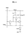
- FIG. 4 is a circuit diagram illustrating an AM-OLED pixel structure according to a preferred embodiment of the present invention.
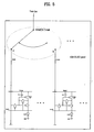
- FIG. 5 is a circuit diagram illustrating an AM-OLED panel according to a comparative example of the present invention.
- FIG. 6 is a timing diagram illustrating a method for driving a flat panel display according to a comparative example of the present invention.
- FIG. 7 is a conceptual diagram illustrating a method for driving a flat panel display when a pre-charging phase is omitted according to the present invention.
- the OLED will be described as a representative current-drive-type light-emitting diode.
- the present invention relates to a display equipped with an OLED panel. More particularly, the present invention relates to a method for driving a large-area and high-gray-level OLED display panel using a TFT and a single-crystal silicon transistor.
- FIG. 3 is a conceptual diagram illustrating a method for driving a flat panel display according to the present invention.
- FIG. 4 is a circuit diagram illustrating an AM-OLED pixel structure according to a preferred embodiment of the present invention.
- FIG. 3 is a conceptual diagram of a single pixel unit. Each pixel is classified into a light-emitting phase and a non-light-emitting phase.
- the present invention is characterized in that a threshold voltage is stored or pre-charged during the non-light-emitting phase or time, and the resultant threshold voltage is stored.
- the non-light-emitting phase or time is indicative of a time other than the OLED light-emitting time caused by a data-current writing operation.
- FIG. 3 A detailed description of the pixel unit shown in FIG. 3 will be described with reference to FIG. 4 .
- FIG. 4 shows an internal structure of a single pixel.
- a method for driving the flat panel display by applying the inventive concept of FIG. 3 to the above-mentioned pixel structure will hereinafter be described.
- the conventional method for driving the flat panel display performs a pre-charging operation within the above-mentioned light-emitting time, and at the same stores a threshold voltage. Therefore, a current-drive phase caused by the writing operation of a data current for an actual light-emitting operation is reduced, such that the light-emitting operation is abnormally executed, resulting in the occurrence of image-quality deterioration.
- the light-emitting operation caused by the data-current writing operation must occur within a given period of time, such that the step for performing the pre-charging simultaneously with storing a threshold voltage is insufficiently executed. As a result, uniformity of each pixel is not achieved, and a brightness lifetime of each pixel is shortened.
- the present invention proposes a method for performing pre-charging of each pixel simultaneously with storing a threshold voltage during the given non-light-emitting time, such that only the light-emitting operation caused by the data-current writing operation during the light-emitting time is executed to solve the problems of the conventional art.
- the present invention is mainly classified into a light-emitting phase and a non-light-emitting phase. If a data driver transmits a pre-charging voltage to a data line, a parasitic capacitor of the data line and a storage capacitor of each pixel form a pre-charging voltage (i.e., a pre-charging phase).
- the data line enters a floating state (also called a float-state), and the data line and the pixel-storage capacitor are charged with electricity via the pixel transistor, having a diode structure, connected to the data line.
- a floating state also called a float-state
- the non-light-emitting phase is switched to the light-emitting phase.
- a current signal is received in the data line via the switched-ON pixel transistor during the light-emitting phase, each pixel emits light at a specific brightness proportional to the received current signal, and the aforementioned operation is called a "Current Driving Phase".
- Each pixel emits light during the non-light-emitting phase and the light-emitting phase, and the aforementioned phases are sequentially repeated for each frame, such that uniform brightness and high-contrast of each pixel are implemented. Also, since the pre-charging operation is sufficiently executed and the threshold voltage is stored, a constant OFF period is created, resulting in the implementation of increased brightness/lifetime of the OLED.
- the method for driving a display panel can also be applied to a cross-drive operation of a MUX-type flat panel display, and a detailed description thereof will hereinafter be described with reference to FIGS. 5 ⁇ 6 .
- the MUX-type flat panel display of FIG. 5 cross-drives the data line using a MUX (Multiplexer) circuit contained in a plurality of data lines, instead of connecting the data line to each pixel.
- MUX Multiplexer
- FIG. 5 is a circuit diagram illustrating an AM-OLED panel designed to drive the panel equipped with the pixel structure of FIG. 4 using the MUX circuit.
- FIG. 6 is a timing diagram illustrating a method for driving the AM-OLED panel of FIG. 5 .
- FIGS. 5 ⁇ 6 A preferred comparative example will be described with reference to FIGS. 5 ⁇ 6 . It is assumed that the present example includes the step for performing the pre-charging operation simultaneously with storing the threshold voltage, and the number of pixels connected to the MUX circuit of FIG. 5 is set to "2" for the convenience of description and better understanding of the present example.
- the MUX circuit cross-selects two data lines A and B.
- the scan line SCAN[n] provides a scan signal associated with the pixel connected to the data line A.
- the scan line SCAN[n+1] is indicative of the next scan signal associated with the aforementioned data line A.
- the scan line SCAN[n]' provides the scan signal associated with the pixel connected to the data line B.
- the scan line SCAN[n+1]' is indicative of the next scan signal associated with the data line B.
- V Data(n) is indicative of a drive waveform for each time zone in association with the data line A.
- V Data(n) is indicative of a drive waveform for each time zone in association with the data line B.
- the MUX circuit of FIG. 5 selects the data line A during the pre-charging phase, at the same time the voltage of the N-th scan line is reduced, transistors T1 and T3 are switched on, and a pre-charging voltage is transmitted from the data driver to the data line of the MUX circuit, the data line and the storage capacitor (Cst) are charged with a pre-charging voltage.
- the transistor T2 and the switched-ON transistor T1 have a diode structure, the T2 transistor is switched off, such that the OLED element is also switched off.
- the present invention is characterized in that the pre-charging voltage is lower than the threshold voltage of a driving TFT.
- the pre-charging operation indicates that electricity is pre-charged to compensate for an insufficient data charging operation due to slow response characteristics of the pixel.
- the present invention applies a pre-charging voltage lower than the threshold voltage of the driving TFT, such that the present invention prevents the data current from flowing into the data line before the capacitor (Cst) is sufficiently charged with electricity.
- the present invention can maintain uniform brightness due to the sufficient electric-charging operation.
- the above-mentioned pre-charging phase may be omitted as necessary.
- Vth Saving Phase acting as the second phase for storing the threshold voltage
- the MUX circuit shown in FIG. 5 selects the data line B during the Vth-Saving phase, such that the data line A enters the floating state.
- the N-th scan line's voltage is reduced in the same manner as in the aforementioned pre-charging phase, such that transistors T1 and T3 are switched on.
- the MUX circuit of FIG. 5 re-selects the data line A during the Current-Driving phase.
- the N-th scan line's voltage is reduced in the same manner as in the above-mentioned first and second phases, such that the T1 and T3 transistors are switched on.
- a data current signal corresponding to the pixel to be driven by the data line is transmitted from the driving TFT to the data line via the transistors T1 and T3, such that a gate-to-source voltage corresponding to the corresponding data current value is formed at the parasitic capacitor of the data line and the storage capacitor of the pixel by the driving TFT having a diode structure.
- the N-th scan line's voltage is increased during the above-mentioned third phase, the voltage formed by the aforementioned increased voltage is stored in the storage capacitor, a corresponding current signal is applied to the OLED, such that the OLED emits light and the light-emitting operation of the OLED is maintained until reaching the next frame.
- the above-mentioned first to third phases are repeatedly driven for each frame, such that a desired image is displayed on the screen.
- the MUX-type AM-OLED panel shown in FIG. 5 is cross-driven as can be seen from FIG. 6 , such that it can be driven without generating unnecessary time-consumption.
- the aforementioned driving method can also be applied to not only the pixel structure of FIG. 4 but also all of current-drive-type pixel structures.
- the present invention is characterized in that the current-drive-type pixel structure has the Pre-Charging phase, the Vth-Saving phase, and the Current-Driving phase.
- the Pre-Charging phase can be omitted as previously stated above, and a detailed description thereof will hereinafter be described with reference to FIG. 7 .
- FIG. 7 is a conceptual diagram illustrating a method for driving a flat panel display when a pre-charging phase is omitted according to the present invention.
- the method for driving the flat panel display according to the present invention is classified into a first case having the pre-charging phase and a second case having no pre-charging phase.
- the upper drawing of FIG. 7 represents the aforementioned first case having the pre-charging phase during the non-light-emitting time, such that the non-light-emitting time includes a pre-charging time and a time for storing the threshold-voltage.
- the lower drawing of FIG. 7 represents the aforementioned second case having no pre-charging phase during the non-light-emitting time, and only the threshold voltage is stored during the non-light-emitting time.
- the aforementioned second case includes a non-light-emitting time for storing the threshold voltage and a light-emitting time caused by the data-current writing operation.
- the method for driving the flat panel display according to the present invention has the following effects.
- the present invention acquires a constant current signal by compensating for a threshold-voltage deviation and a mobility deviation of the pixel's driving TFT, such that it increases uniformity and improves image quality.
- the present invention solves the pre-charging problems of the conventional current-drive method.
- the present invention allows the OLED to have a predetermined OFF time, and recovers characteristics of the OLED element. Also, the present invention reduces the influence of heat generated by power consumed by the OLED element, and delays deterioration of the element characteristics, such that it increases the lifetime of the OLED element.
Landscapes
- Engineering & Computer Science (AREA)
- Physics & Mathematics (AREA)
- Computer Hardware Design (AREA)
- General Physics & Mathematics (AREA)
- Theoretical Computer Science (AREA)
- Electroluminescent Light Sources (AREA)
- Control Of Indicators Other Than Cathode Ray Tubes (AREA)
- Control Of El Displays (AREA)
Claims (4)
- Flachbildschirmanzeigevorrichtung, die mehrere Pixel enthält, wobei jedes Pixel mit einer Abtastleitung (scan[n]); einer Leistungsversorgungsleitung (VDD-EL); und einer Datenleitung (Data[n]) verbunden ist; und einen Pixeltransistor (Driving TFT), der Gate-, Source- und Drain-Anschlüsse besitzt; einen ersten bis dritten Schalttransistor (T1 bis T3), wovon jeder Gate-, Source- und Drain-Anschlüsse besitzt; einen Speicherkondensator (Cst); und ein lichtaussendendes Element (OLED) umfasst, wobei der Gate-Anschluss des dritten Transistors (T3) mit der Abtastleitung (scan[n]) verbunden ist, der Source-Anschluss des dritten Transistors (T3) mit der Datenleitung (Data[n]) verbunden ist, der Drain-Anschluss des dritten Transistors (T3) mit dem Gate-Anschluss des Pixeltransistors (Driving TFT) verbunden ist, der Source-Anschluss des ersten Schalttransistors (T1) mit dem Gate-Anschluss des Pixeltransistors (Driving TFT) verbunden ist, der Gate-Anschluss des ersten Schalttransistors (T1) mit der Abtastleitung (scan[n]) verbunden ist, der Drain-Anschluss des ersten Schalttransistors (T1) mit dem Drain-Anschluss des Pixeltransistors (Driving-TFT) verbunden ist, der Speicherkondensator zwischen der Leistungsversorgungsleitung (VDD-EL) und dem Gate-Anschluss des Pixeltransistors (Driving-TFT) angeschlossen ist, der Source-Anschluss des Pixeltransistors (Driving-TFT) mit der Leistungsversorgungsleitung (VDD-EL) verbunden ist, der Source-Anschluss des zweiten Schalttransistors (T2) mit dem Drain-Anschluss des Pixeltransistors (Driving TFT) verbunden ist und das lichtaussendende Element (OLED) zwischen dem Drain-Anschluss des zweiten Schalttransistors (T2) und Masse angeschlossen ist, wobei jedes Pixel dadurch gekennzeichnet ist, dass der Gate-Anschluss des zweiten Schalttransistors (T2) mit dem Drain-Anschluss des dritten Transistors (T3) verbunden ist.
- Verfahren zum Ansteuern einer Flachbildschirmanzeigevorrichtung nach Anspruch 1, das die Schritte umfasst:Eintreten in einen Schwebezustand durch die Datenleitung (Data[n]) und Einspeisen eines Abtastsignals in die Abtastleitung (scan [n]), um den ersten und den dritten Schalttransistor (T1, T3) durchzuschalten, so dass der Speicherkondensator über den Pixeltransistor (Driving TFT), der eine Diodenstruktur besitzt und mit der Datenleitung verbunden ist, mit Elektrizität geladen wird,Einspeisen eines Ansteuerstromsignals in jedes Pixel über die Datenleitung (Data [n]), wenn die gespeicherte Spannung die Schwellwertspannung des Pixeltransistors (Driving TFT) erreicht.
- Verfahren nach Anspruch 2, das ferner den Schritt umfasst:Liefern einer Vorladungsspannung über die Datenleitung (Data [n]) vor dem Schritt, in dem der Datenleitung (Data [n]) ermöglicht wird, in einen Schwebezustand einzutreten, an den Speicherkondensator.
- Verfahren nach Anspruch 3, wobei die Vorladungsspannung kleiner als die Schwellwertspannung des Pixeltransistors (Driving TFT) ist.
Priority Applications (1)
| Application Number | Priority Date | Filing Date | Title |
|---|---|---|---|
| EP10171280.0A EP2239724B1 (de) | 2005-05-17 | 2006-05-17 | Ansteuerverfahren für einen Flachbildschirm |
Applications Claiming Priority (1)
| Application Number | Priority Date | Filing Date | Title |
|---|---|---|---|
| KR1020050041204A KR100762138B1 (ko) | 2005-05-17 | 2005-05-17 | 평판 디스플레이 패널의 구동 방법 |
Related Child Applications (2)
| Application Number | Title | Priority Date | Filing Date |
|---|---|---|---|
| EP10171280.0A Division EP2239724B1 (de) | 2005-05-17 | 2006-05-17 | Ansteuerverfahren für einen Flachbildschirm |
| EP10171280.0 Division-Into | 2010-07-29 |
Publications (3)
| Publication Number | Publication Date |
|---|---|
| EP1724748A2 EP1724748A2 (de) | 2006-11-22 |
| EP1724748A3 EP1724748A3 (de) | 2010-03-17 |
| EP1724748B1 true EP1724748B1 (de) | 2013-12-25 |
Family
ID=36636215
Family Applications (2)
| Application Number | Title | Priority Date | Filing Date |
|---|---|---|---|
| EP06010197.9A Active EP1724748B1 (de) | 2005-05-17 | 2006-05-17 | Ansteuerverfahren für einen Flachbildschirm |
| EP10171280.0A Active EP2239724B1 (de) | 2005-05-17 | 2006-05-17 | Ansteuerverfahren für einen Flachbildschirm |
Family Applications After (1)
| Application Number | Title | Priority Date | Filing Date |
|---|---|---|---|
| EP10171280.0A Active EP2239724B1 (de) | 2005-05-17 | 2006-05-17 | Ansteuerverfahren für einen Flachbildschirm |
Country Status (4)
| Country | Link |
|---|---|
| US (1) | US8054251B2 (de) |
| EP (2) | EP1724748B1 (de) |
| KR (1) | KR100762138B1 (de) |
| CN (1) | CN100576299C (de) |
Families Citing this family (13)
| Publication number | Priority date | Publication date | Assignee | Title |
|---|---|---|---|---|
| KR100824852B1 (ko) * | 2006-12-20 | 2008-04-23 | 삼성에스디아이 주식회사 | 유기 전계 발광 표시 장치 |
| KR100873705B1 (ko) | 2007-06-22 | 2008-12-12 | 삼성모바일디스플레이주식회사 | 유기전계발광표시장치 및 그의 제조방법 |
| US8264428B2 (en) * | 2007-09-20 | 2012-09-11 | Lg Display Co., Ltd. | Pixel driving method and apparatus for organic light emitting device |
| US20090091264A1 (en) * | 2007-10-04 | 2009-04-09 | Himax Technologies Limited | Pixel circuit |
| KR20090132858A (ko) | 2008-06-23 | 2009-12-31 | 삼성전자주식회사 | 표시 장치 및 그 구동 방법 |
| JP2010048866A (ja) * | 2008-08-19 | 2010-03-04 | Sony Corp | 表示装置、表示駆動方法 |
| KR101518324B1 (ko) | 2008-09-24 | 2015-05-11 | 삼성디스플레이 주식회사 | 표시 장치 및 그 구동 방법 |
| KR101525807B1 (ko) | 2009-02-05 | 2015-06-05 | 삼성디스플레이 주식회사 | 표시 장치및 그 구동 방법 |
| JP5439912B2 (ja) * | 2009-04-01 | 2014-03-12 | セイコーエプソン株式会社 | 電気光学装置及びその駆動方法並びに電子機器 |
| CN102651195B (zh) * | 2011-09-14 | 2014-08-27 | 京东方科技集团股份有限公司 | 用于补偿发光不均匀的oled像素结构及驱动方法 |
| JP6138244B2 (ja) * | 2013-04-23 | 2017-05-31 | シャープ株式会社 | 表示装置およびその駆動電流検出方法 |
| WO2021226864A1 (zh) * | 2020-05-13 | 2021-11-18 | 京东方科技集团股份有限公司 | 像素驱动方法、显示驱动方法和显示基板 |
| CN112530369B (zh) * | 2020-12-25 | 2022-03-25 | 京东方科技集团股份有限公司 | 一种显示面板、显示装置以及驱动方法 |
Citations (1)
| Publication number | Priority date | Publication date | Assignee | Title |
|---|---|---|---|---|
| US20050067971A1 (en) * | 2003-09-29 | 2005-03-31 | Michael Gillis Kane | Pixel circuit for an active matrix organic light-emitting diode display |
Family Cites Families (9)
| Publication number | Priority date | Publication date | Assignee | Title |
|---|---|---|---|---|
| JP2002108284A (ja) * | 2000-09-28 | 2002-04-10 | Nec Corp | 有機el表示装置及びその駆動方法 |
| KR100819138B1 (ko) * | 2001-08-25 | 2008-04-21 | 엘지.필립스 엘시디 주식회사 | 일렉트로 루미네센스 패널의 구동장치 및 그 구동방법 |
| KR100649243B1 (ko) | 2002-03-21 | 2006-11-24 | 삼성에스디아이 주식회사 | 유기 전계발광 표시 장치 및 그 구동 방법 |
| KR100515318B1 (ko) * | 2003-07-30 | 2005-09-15 | 삼성에스디아이 주식회사 | 표시 장치와 그 구동 방법 |
| JP2005099715A (ja) | 2003-08-29 | 2005-04-14 | Seiko Epson Corp | 電子回路の駆動方法、電子回路、電子装置、電気光学装置、電子機器および電子装置の駆動方法 |
| KR20050037303A (ko) * | 2003-10-18 | 2005-04-21 | 삼성오엘이디 주식회사 | 예비 충전이 선택적으로 수행되는 전계발광 디스플레이패널의 구동방법 |
| JP4049085B2 (ja) * | 2003-11-11 | 2008-02-20 | セイコーエプソン株式会社 | 画素回路の駆動方法、画素回路および電子機器 |
| US7333078B2 (en) * | 2003-12-29 | 2008-02-19 | Solomon Systech Limited | Driving system and method for electroluminescence displays |
| KR200378027Y1 (ko) * | 2004-12-11 | 2005-03-11 | 주식회사 필톤 | 항균 기능을 갖는 전자카드 |
-
2005
- 2005-05-17 KR KR1020050041204A patent/KR100762138B1/ko active IP Right Grant
-
2006
- 2006-05-17 EP EP06010197.9A patent/EP1724748B1/de active Active
- 2006-05-17 CN CN200610084783A patent/CN100576299C/zh active Active
- 2006-05-17 EP EP10171280.0A patent/EP2239724B1/de active Active
- 2006-05-17 US US11/434,819 patent/US8054251B2/en active Active
Patent Citations (1)
| Publication number | Priority date | Publication date | Assignee | Title |
|---|---|---|---|---|
| US20050067971A1 (en) * | 2003-09-29 | 2005-03-31 | Michael Gillis Kane | Pixel circuit for an active matrix organic light-emitting diode display |
Also Published As
| Publication number | Publication date |
|---|---|
| EP1724748A3 (de) | 2010-03-17 |
| CN1866339A (zh) | 2006-11-22 |
| US8054251B2 (en) | 2011-11-08 |
| EP2239724A1 (de) | 2010-10-13 |
| US20060262051A1 (en) | 2006-11-23 |
| EP2239724B1 (de) | 2015-07-08 |
| EP1724748A2 (de) | 2006-11-22 |
| CN100576299C (zh) | 2009-12-30 |
| KR20060118826A (ko) | 2006-11-24 |
| KR100762138B1 (ko) | 2007-10-02 |
Similar Documents
| Publication | Publication Date | Title |
|---|---|---|
| EP1724748B1 (de) | Ansteuerverfahren für einen Flachbildschirm | |
| US7277071B2 (en) | Luminescent display, and driving method and pixel circuit thereof, and display device | |
| EP1585100B1 (de) | Elektrolumineszenzanzeigevorrichtung und Pixelschaltung dafür | |
| EP2192571B1 (de) | Organische lichtemittierende Anzeigevorrichtung und Antriebsverfahren dafür | |
| KR101030004B1 (ko) | 화소 회로 및 이를 이용한 유기전계발광 표시 장치 | |
| CN100369096C (zh) | 发光显示器、显示屏及其驱动方法 | |
| US7358938B2 (en) | Circuit and method for driving pixel of organic electroluminescent display | |
| KR101042956B1 (ko) | 화소 회로 및 이를 이용한 유기전계발광 표시장치 | |
| US7129643B2 (en) | Light-emitting display, driving method thereof, and light-emitting display panel | |
| KR101030002B1 (ko) | 화소 회로 및 이를 이용한 유기전계발광 표시 장치 | |
| EP1646032B1 (de) | Pixelschaltung für ein OLED Display mit automatischer Kompensation der Schwellenspannung | |
| EP1473689A2 (de) | Pixelschaltung, Anzeigetafel, Anzeigevorrichtung und Steuerverfahren dafür | |
| US20110115772A1 (en) | Pixel Circuit and Organic Electroluminescent Display Apparatus Using the Same | |
| KR101058107B1 (ko) | 화소 회로 및 이를 이용한 유기 발광 표시장치 | |
| WO2003077229A1 (en) | Organic electroluminescent display and driving method thereof | |
| KR20070111634A (ko) | 유기전계발광표시장치의 화소 회로 | |
| JP2005157244A (ja) | 発光表示装置及びその表示パネルと駆動方法 | |
| JP2005134880A (ja) | 画像表示装置,その駆動方法,及びプリチャージ電圧設定方法 | |
| US7109982B2 (en) | Display panel and driving method thereof | |
| JP2005141195A (ja) | 画像表示装置及びその駆動方法 | |
| KR20040021753A (ko) | 유기 전계발광 표시장치 및 그의 구동방법 | |
| KR100698709B1 (ko) | 샘플/홀딩 회로 및 이를 이용한 유기 전계발광 표시장치 |
Legal Events
| Date | Code | Title | Description |
|---|---|---|---|
| PUAI | Public reference made under article 153(3) epc to a published international application that has entered the european phase |
Free format text: ORIGINAL CODE: 0009012 |
|
| 17P | Request for examination filed |
Effective date: 20060517 |
|
| AK | Designated contracting states |
Kind code of ref document: A2 Designated state(s): AT BE BG CH CY CZ DE DK EE ES FI FR GB GR HU IE IS IT LI LT LU LV MC NL PL PT RO SE SI SK TR |
|
| AX | Request for extension of the european patent |
Extension state: AL BA HR MK YU |
|
| RAP1 | Party data changed (applicant data changed or rights of an application transferred) |
Owner name: LG DISPLAY CO., LTD. |
|
| PUAL | Search report despatched |
Free format text: ORIGINAL CODE: 0009013 |
|
| AK | Designated contracting states |
Kind code of ref document: A3 Designated state(s): AT BE BG CH CY CZ DE DK EE ES FI FR GB GR HU IE IS IT LI LT LU LV MC NL PL PT RO SE SI SK TR |
|
| AX | Request for extension of the european patent |
Extension state: AL BA HR MK YU |
|
| 17Q | First examination report despatched |
Effective date: 20100706 |
|
| AKX | Designation fees paid |
Designated state(s): DE FR GB NL |
|
| GRAP | Despatch of communication of intention to grant a patent |
Free format text: ORIGINAL CODE: EPIDOSNIGR1 |
|
| INTG | Intention to grant announced |
Effective date: 20130718 |
|
| GRAS | Grant fee paid |
Free format text: ORIGINAL CODE: EPIDOSNIGR3 |
|
| GRAA | (expected) grant |
Free format text: ORIGINAL CODE: 0009210 |
|
| AK | Designated contracting states |
Kind code of ref document: B1 Designated state(s): DE FR GB NL |
|
| REG | Reference to a national code |
Ref country code: GB Ref legal event code: FG4D |
|
| REG | Reference to a national code |
Ref country code: DE Ref legal event code: R096 Ref document number: 602006039739 Country of ref document: DE Effective date: 20140213 |
|
| REG | Reference to a national code |
Ref country code: NL Ref legal event code: T3 |
|
| REG | Reference to a national code |
Ref country code: DE Ref legal event code: R097 Ref document number: 602006039739 Country of ref document: DE |
|
| PLBE | No opposition filed within time limit |
Free format text: ORIGINAL CODE: 0009261 |
|
| STAA | Information on the status of an ep patent application or granted ep patent |
Free format text: STATUS: NO OPPOSITION FILED WITHIN TIME LIMIT |
|
| 26N | No opposition filed |
Effective date: 20140926 |
|
| REG | Reference to a national code |
Ref country code: DE Ref legal event code: R097 Ref document number: 602006039739 Country of ref document: DE Effective date: 20140926 |
|
| REG | Reference to a national code |
Ref country code: FR Ref legal event code: PLFP Year of fee payment: 11 |
|
| REG | Reference to a national code |
Ref country code: FR Ref legal event code: PLFP Year of fee payment: 12 |
|
| REG | Reference to a national code |
Ref country code: FR Ref legal event code: PLFP Year of fee payment: 13 |
|
| PGFP | Annual fee paid to national office [announced via postgrant information from national office to epo] |
Ref country code: FR Payment date: 20230321 Year of fee payment: 18 |
|
| PGFP | Annual fee paid to national office [announced via postgrant information from national office to epo] |
Ref country code: DE Payment date: 20230320 Year of fee payment: 18 |
|
| PGFP | Annual fee paid to national office [announced via postgrant information from national office to epo] |
Ref country code: NL Payment date: 20240321 Year of fee payment: 19 |
|
| PGFP | Annual fee paid to national office [announced via postgrant information from national office to epo] |
Ref country code: GB Payment date: 20240320 Year of fee payment: 19 |