EP1722009A1 - Thin wear resistant coating - Google Patents
Thin wear resistant coating Download PDFInfo
- Publication number
- EP1722009A1 EP1722009A1 EP06445019A EP06445019A EP1722009A1 EP 1722009 A1 EP1722009 A1 EP 1722009A1 EP 06445019 A EP06445019 A EP 06445019A EP 06445019 A EP06445019 A EP 06445019A EP 1722009 A1 EP1722009 A1 EP 1722009A1
- Authority
- EP
- European Patent Office
- Prior art keywords
- peak
- elements
- layer
- phase
- cutting tool
- Prior art date
- Legal status (The legal status is an assumption and is not a legal conclusion. Google has not performed a legal analysis and makes no representation as to the accuracy of the status listed.)
- Granted
Links
Images
Classifications
-
- C—CHEMISTRY; METALLURGY
- C23—COATING METALLIC MATERIAL; COATING MATERIAL WITH METALLIC MATERIAL; CHEMICAL SURFACE TREATMENT; DIFFUSION TREATMENT OF METALLIC MATERIAL; COATING BY VACUUM EVAPORATION, BY SPUTTERING, BY ION IMPLANTATION OR BY CHEMICAL VAPOUR DEPOSITION, IN GENERAL; INHIBITING CORROSION OF METALLIC MATERIAL OR INCRUSTATION IN GENERAL
- C23C—COATING METALLIC MATERIAL; COATING MATERIAL WITH METALLIC MATERIAL; SURFACE TREATMENT OF METALLIC MATERIAL BY DIFFUSION INTO THE SURFACE, BY CHEMICAL CONVERSION OR SUBSTITUTION; COATING BY VACUUM EVAPORATION, BY SPUTTERING, BY ION IMPLANTATION OR BY CHEMICAL VAPOUR DEPOSITION, IN GENERAL
- C23C30/00—Coating with metallic material characterised only by the composition of the metallic material, i.e. not characterised by the coating process
-
- C—CHEMISTRY; METALLURGY
- C22—METALLURGY; FERROUS OR NON-FERROUS ALLOYS; TREATMENT OF ALLOYS OR NON-FERROUS METALS
- C22C—ALLOYS
- C22C27/00—Alloys based on rhenium or a refractory metal not mentioned in groups C22C14/00 or C22C16/00
-
- C—CHEMISTRY; METALLURGY
- C23—COATING METALLIC MATERIAL; COATING MATERIAL WITH METALLIC MATERIAL; CHEMICAL SURFACE TREATMENT; DIFFUSION TREATMENT OF METALLIC MATERIAL; COATING BY VACUUM EVAPORATION, BY SPUTTERING, BY ION IMPLANTATION OR BY CHEMICAL VAPOUR DEPOSITION, IN GENERAL; INHIBITING CORROSION OF METALLIC MATERIAL OR INCRUSTATION IN GENERAL
- C23C—COATING METALLIC MATERIAL; COATING MATERIAL WITH METALLIC MATERIAL; SURFACE TREATMENT OF METALLIC MATERIAL BY DIFFUSION INTO THE SURFACE, BY CHEMICAL CONVERSION OR SUBSTITUTION; COATING BY VACUUM EVAPORATION, BY SPUTTERING, BY ION IMPLANTATION OR BY CHEMICAL VAPOUR DEPOSITION, IN GENERAL
- C23C14/00—Coating by vacuum evaporation, by sputtering or by ion implantation of the coating forming material
- C23C14/06—Coating by vacuum evaporation, by sputtering or by ion implantation of the coating forming material characterised by the coating material
- C23C14/0641—Nitrides
- C23C14/0647—Boron nitride
-
- C—CHEMISTRY; METALLURGY
- C23—COATING METALLIC MATERIAL; COATING MATERIAL WITH METALLIC MATERIAL; CHEMICAL SURFACE TREATMENT; DIFFUSION TREATMENT OF METALLIC MATERIAL; COATING BY VACUUM EVAPORATION, BY SPUTTERING, BY ION IMPLANTATION OR BY CHEMICAL VAPOUR DEPOSITION, IN GENERAL; INHIBITING CORROSION OF METALLIC MATERIAL OR INCRUSTATION IN GENERAL
- C23C—COATING METALLIC MATERIAL; COATING MATERIAL WITH METALLIC MATERIAL; SURFACE TREATMENT OF METALLIC MATERIAL BY DIFFUSION INTO THE SURFACE, BY CHEMICAL CONVERSION OR SUBSTITUTION; COATING BY VACUUM EVAPORATION, BY SPUTTERING, BY ION IMPLANTATION OR BY CHEMICAL VAPOUR DEPOSITION, IN GENERAL
- C23C14/00—Coating by vacuum evaporation, by sputtering or by ion implantation of the coating forming material
- C23C14/06—Coating by vacuum evaporation, by sputtering or by ion implantation of the coating forming material characterised by the coating material
- C23C14/0641—Nitrides
- C23C14/0658—Carbon nitride
-
- C—CHEMISTRY; METALLURGY
- C23—COATING METALLIC MATERIAL; COATING MATERIAL WITH METALLIC MATERIAL; CHEMICAL SURFACE TREATMENT; DIFFUSION TREATMENT OF METALLIC MATERIAL; COATING BY VACUUM EVAPORATION, BY SPUTTERING, BY ION IMPLANTATION OR BY CHEMICAL VAPOUR DEPOSITION, IN GENERAL; INHIBITING CORROSION OF METALLIC MATERIAL OR INCRUSTATION IN GENERAL
- C23C—COATING METALLIC MATERIAL; COATING MATERIAL WITH METALLIC MATERIAL; SURFACE TREATMENT OF METALLIC MATERIAL BY DIFFUSION INTO THE SURFACE, BY CHEMICAL CONVERSION OR SUBSTITUTION; COATING BY VACUUM EVAPORATION, BY SPUTTERING, BY ION IMPLANTATION OR BY CHEMICAL VAPOUR DEPOSITION, IN GENERAL
- C23C14/00—Coating by vacuum evaporation, by sputtering or by ion implantation of the coating forming material
- C23C14/06—Coating by vacuum evaporation, by sputtering or by ion implantation of the coating forming material characterised by the coating material
- C23C14/0664—Carbonitrides
-
- C—CHEMISTRY; METALLURGY
- C23—COATING METALLIC MATERIAL; COATING MATERIAL WITH METALLIC MATERIAL; CHEMICAL SURFACE TREATMENT; DIFFUSION TREATMENT OF METALLIC MATERIAL; COATING BY VACUUM EVAPORATION, BY SPUTTERING, BY ION IMPLANTATION OR BY CHEMICAL VAPOUR DEPOSITION, IN GENERAL; INHIBITING CORROSION OF METALLIC MATERIAL OR INCRUSTATION IN GENERAL
- C23C—COATING METALLIC MATERIAL; COATING MATERIAL WITH METALLIC MATERIAL; SURFACE TREATMENT OF METALLIC MATERIAL BY DIFFUSION INTO THE SURFACE, BY CHEMICAL CONVERSION OR SUBSTITUTION; COATING BY VACUUM EVAPORATION, BY SPUTTERING, BY ION IMPLANTATION OR BY CHEMICAL VAPOUR DEPOSITION, IN GENERAL
- C23C14/00—Coating by vacuum evaporation, by sputtering or by ion implantation of the coating forming material
- C23C14/06—Coating by vacuum evaporation, by sputtering or by ion implantation of the coating forming material characterised by the coating material
- C23C14/0676—Oxynitrides
-
- C—CHEMISTRY; METALLURGY
- C23—COATING METALLIC MATERIAL; COATING MATERIAL WITH METALLIC MATERIAL; CHEMICAL SURFACE TREATMENT; DIFFUSION TREATMENT OF METALLIC MATERIAL; COATING BY VACUUM EVAPORATION, BY SPUTTERING, BY ION IMPLANTATION OR BY CHEMICAL VAPOUR DEPOSITION, IN GENERAL; INHIBITING CORROSION OF METALLIC MATERIAL OR INCRUSTATION IN GENERAL
- C23C—COATING METALLIC MATERIAL; COATING MATERIAL WITH METALLIC MATERIAL; SURFACE TREATMENT OF METALLIC MATERIAL BY DIFFUSION INTO THE SURFACE, BY CHEMICAL CONVERSION OR SUBSTITUTION; COATING BY VACUUM EVAPORATION, BY SPUTTERING, BY ION IMPLANTATION OR BY CHEMICAL VAPOUR DEPOSITION, IN GENERAL
- C23C28/00—Coating for obtaining at least two superposed coatings either by methods not provided for in a single one of groups C23C2/00 - C23C26/00 or by combinations of methods provided for in subclasses C23C and C25C or C25D
- C23C28/04—Coating for obtaining at least two superposed coatings either by methods not provided for in a single one of groups C23C2/00 - C23C26/00 or by combinations of methods provided for in subclasses C23C and C25C or C25D only coatings of inorganic non-metallic material
- C23C28/042—Coating for obtaining at least two superposed coatings either by methods not provided for in a single one of groups C23C2/00 - C23C26/00 or by combinations of methods provided for in subclasses C23C and C25C or C25D only coatings of inorganic non-metallic material including a refractory ceramic layer, e.g. refractory metal oxides, ZrO2, rare earth oxides
-
- C—CHEMISTRY; METALLURGY
- C23—COATING METALLIC MATERIAL; COATING MATERIAL WITH METALLIC MATERIAL; CHEMICAL SURFACE TREATMENT; DIFFUSION TREATMENT OF METALLIC MATERIAL; COATING BY VACUUM EVAPORATION, BY SPUTTERING, BY ION IMPLANTATION OR BY CHEMICAL VAPOUR DEPOSITION, IN GENERAL; INHIBITING CORROSION OF METALLIC MATERIAL OR INCRUSTATION IN GENERAL
- C23C—COATING METALLIC MATERIAL; COATING MATERIAL WITH METALLIC MATERIAL; SURFACE TREATMENT OF METALLIC MATERIAL BY DIFFUSION INTO THE SURFACE, BY CHEMICAL CONVERSION OR SUBSTITUTION; COATING BY VACUUM EVAPORATION, BY SPUTTERING, BY ION IMPLANTATION OR BY CHEMICAL VAPOUR DEPOSITION, IN GENERAL
- C23C28/00—Coating for obtaining at least two superposed coatings either by methods not provided for in a single one of groups C23C2/00 - C23C26/00 or by combinations of methods provided for in subclasses C23C and C25C or C25D
- C23C28/04—Coating for obtaining at least two superposed coatings either by methods not provided for in a single one of groups C23C2/00 - C23C26/00 or by combinations of methods provided for in subclasses C23C and C25C or C25D only coatings of inorganic non-metallic material
- C23C28/044—Coating for obtaining at least two superposed coatings either by methods not provided for in a single one of groups C23C2/00 - C23C26/00 or by combinations of methods provided for in subclasses C23C and C25C or C25D only coatings of inorganic non-metallic material coatings specially adapted for cutting tools or wear applications
-
- C—CHEMISTRY; METALLURGY
- C23—COATING METALLIC MATERIAL; COATING MATERIAL WITH METALLIC MATERIAL; CHEMICAL SURFACE TREATMENT; DIFFUSION TREATMENT OF METALLIC MATERIAL; COATING BY VACUUM EVAPORATION, BY SPUTTERING, BY ION IMPLANTATION OR BY CHEMICAL VAPOUR DEPOSITION, IN GENERAL; INHIBITING CORROSION OF METALLIC MATERIAL OR INCRUSTATION IN GENERAL
- C23C—COATING METALLIC MATERIAL; COATING MATERIAL WITH METALLIC MATERIAL; SURFACE TREATMENT OF METALLIC MATERIAL BY DIFFUSION INTO THE SURFACE, BY CHEMICAL CONVERSION OR SUBSTITUTION; COATING BY VACUUM EVAPORATION, BY SPUTTERING, BY ION IMPLANTATION OR BY CHEMICAL VAPOUR DEPOSITION, IN GENERAL
- C23C28/00—Coating for obtaining at least two superposed coatings either by methods not provided for in a single one of groups C23C2/00 - C23C26/00 or by combinations of methods provided for in subclasses C23C and C25C or C25D
- C23C28/04—Coating for obtaining at least two superposed coatings either by methods not provided for in a single one of groups C23C2/00 - C23C26/00 or by combinations of methods provided for in subclasses C23C and C25C or C25D only coatings of inorganic non-metallic material
- C23C28/048—Coating for obtaining at least two superposed coatings either by methods not provided for in a single one of groups C23C2/00 - C23C26/00 or by combinations of methods provided for in subclasses C23C and C25C or C25D only coatings of inorganic non-metallic material with layers graded in composition or physical properties
-
- C—CHEMISTRY; METALLURGY
- C23—COATING METALLIC MATERIAL; COATING MATERIAL WITH METALLIC MATERIAL; CHEMICAL SURFACE TREATMENT; DIFFUSION TREATMENT OF METALLIC MATERIAL; COATING BY VACUUM EVAPORATION, BY SPUTTERING, BY ION IMPLANTATION OR BY CHEMICAL VAPOUR DEPOSITION, IN GENERAL; INHIBITING CORROSION OF METALLIC MATERIAL OR INCRUSTATION IN GENERAL
- C23C—COATING METALLIC MATERIAL; COATING MATERIAL WITH METALLIC MATERIAL; SURFACE TREATMENT OF METALLIC MATERIAL BY DIFFUSION INTO THE SURFACE, BY CHEMICAL CONVERSION OR SUBSTITUTION; COATING BY VACUUM EVAPORATION, BY SPUTTERING, BY ION IMPLANTATION OR BY CHEMICAL VAPOUR DEPOSITION, IN GENERAL
- C23C30/00—Coating with metallic material characterised only by the composition of the metallic material, i.e. not characterised by the coating process
- C23C30/005—Coating with metallic material characterised only by the composition of the metallic material, i.e. not characterised by the coating process on hard metal substrates
Definitions
- the present invention relates to a cutting tool for machining by chip removal consisting of a substrate of cemented carbide, cermet, ceramics, cubic boron nitride based material, or high speed steel, and a hard and wear resistant refractory coating of which at least one layer comprises a hexagonal MeX-phase formed in-situ during the deposition either as a single phase or by co-deposition together with a second phase.
- This finding can be used in several ways giving a high degree of possibilities to tailoring the properties of the finished tool, for example as hexagonal structure particles in a coating matrix of another type, or of the same type, of crystal structure, or as separate layers within a multilayer superstructure. Since the hexagonal type of structure has different mechanical and chemical properties than for instance a cubic structure, the combination of different types of crystallites can give completely new properties compared to a single structure material.
- PVD-layers used today for metal cutting for machining by chip removal consists of crystalline TiN, Ti(C,N), and (Ti,A1)N with a cubic NaCl type structure.
- a metastable (Ti,Al)N layer will at elevated temperature, during heat treatment or at service if sufficient amount of energy is supplied, phase separate into c-TiN and h-AIN.
- These precipitates of a h-AIN and/or c-AIN can act as hardeners in the layers.
- layers containing h-MeX phase can be obtained which compared to the prior art display enhanced performance in metal cutting.
- the layers comprise crystals of h-MeX with or without the co-existence of c-NaCl type structures of nitrides and/or carbides and/or oxides.
- the layers are deposited using PVD-technique, preferably by arc evaporation.
- a cutting tool for machining by chip removal comprising a body of a hard alloy of cemented carbide, cermet, ceramics, cubic boron nitride based material, or high speed steel, onto which a wear resistant coating is deposited composed of one or more layers of refractory compounds comprising at least one layer being composed of crystals of h-MeX phase.
- Additional layers are composed of nitrides and/or carbides and/or oxides with the elements chosen from Ti, Zr, Hf, V, Nb, Ta, Cr, Mo, W, Si and Al, grown using physical vapour deposition (PVD), or other deposition technologies such as plasma enhanced chemical vapour deposition (PACVD) and/or chemical vapour deposition (CVD).
- PVD physical vapour deposition
- PVD plasma enhanced chemical vapour deposition
- CVD chemical vapour deposition
- Tools according to the present invention are particularly useful in metal cutting applications where the chip thickness is small and the work material is hard such as copy milling using solid end mills, insert milling cutters or drilling of hardened steels.
- the h-MeX layer(s) comprise(s) crystals of h-MeX phase.
- the composition shall be described as Me1 a Me2 1-a X b where Me1 is one or more of the elements V, Cr, Nb, and Ta and Me2 is one or more of the elements Ti, Zr, Hf, Al, and Si and a > 0.5 and X one or more of the elements N, C, O and B.
- the non-metal to metal atomic ratio, here defined as R (at-% X)/(at-% Me1 + at-% Me2) of the h-(Me1,Me2)X phase, is between 0.5 and 1.0, preferably between 0.75 and 1.0.
- the h-MeX layer comprising h-(Me1,Me2)X phase is characterised by:
- the layer comprising h-(Me1,Me2)X has a considerably increased hardness compared to a cubic single phase layer of a NaCl type c-MeX structure, see Example 1, as demonstrated by the system of h-(Nb,Zr)N and c-(Nb,Zr)N.
- the total coating thickness if the h-(Me1,Me2)X containing layer(s) according to the present invention are combined with other layer(s), is between 0.1 and 15 ⁇ m, preferably between 0.5 and 12 ⁇ m with the total thickness of the non h-(Me1,Me2)X containing layer(s) varying between 0.5 and 10 ⁇ m.
- the h-(Me1,Me2)X containing layer(s), between 0.1 and 2 ⁇ m thickness are one of one to five different materials in a 1.0 to 15 ⁇ m thick multilayer coating consisting of individually 2-500, preferably 5-200, layers.
- the h-(Me1,Me2)X containing layer(s) of 0.5 and 20 ⁇ m thickness can be deposited on top of a CVD coating which may comprise one or more layer(s) of crystalline Al 2 O 3 .
- At least one h-(Me1,Me2)X containing layer(s) of 0.1 and 1.0 ⁇ m thickness is used for metal cutting application where the chip thickness is very small.
- the method used to grow the layers, comprising h-(Me1,Me2)X phase of the present invention, here exemplified by the system Nb-Zr-N, is based on arc evaporation of an alloyed, or composite cathode, under the following conditions:
- the Nb-Zr cathode composition is >70 at-% Nb, preferably >80 at-% Nb and balance of Zr.
- the evaporation current is between 50 A and 200 A depending on cathode size and cathode material. When using cathodes of 63 mm in diameter the evaporation current is preferably between 70 A and 140 A.
- the substrate bias is between -10 V and -300 V, preferably between -40 V and -120 V.
- the deposition temperature is between 400°C and 700°C, preferably between 500°C and 700°C.
- the evaporation current is preferably between 80 A and 140 A for Nb and between 60 A and 100 A for Zr.
- the arc current and the number of cathodes per element has to be optimised properly.
- an Ar+N 2 atmosphere consisting of 0-50 vol-% Ar, preferably 0-20 vol-%, at a total pressure of 0.5 Pa to 9.0 Pa, preferably 1.5 Pa to 5.0 Pa, is used.
- X includes C and O
- carbon and/or oxygen containing gases have to be added to the N 2 and/or Ar+N 2 atmosphere (e.g. C 2 H 2 , CH 4 , CO, CO 2 , O 2 ).
- X also includes boron it could be added either by alloying the target with boron or by adding a boron containing gas to the atmosphere.
- the deposition rate should not be too high, here below about 4 ⁇ m/h in one fold rotation, with two Nb cathodes separated by 180°, or about 1.5 ⁇ m/h at three fold rotation.
- the deposition rates given above, which actually are average values and not the key parameter, are to be seen as rough guidelines at a deposition temperature of 530°C. When using a higher deposition rate a higher deposition temperature will also be needed.
- layer(s) containing h-(Me1,Me2)X phase of the type described above could also be possible using V and/or Ta as Me1 due to similarities with Nb.
- Using Ti, Zr, and Hf, as Me2, as alloying elements should also be valid using a maximum alloying content preferably less than 20 at-%, most preferably less than 15 at-%, of the total metal content, based on reported hardness versus composition values in Table 1 for the Nb-Zr-N system. Examples on this alloying route is h-(V,Nb,Ta)N, h-(V,Nb,Ta) 1-x (Ti,Zr,Hf) x N with x preferably ⁇ 0.2 and most preferably ⁇ 0.15.
- nitrides are preferred compared to carbonitrides and carbides. Additionally improved oxidation resistance could be achieved by alloying with one or more of the Ti, Al and Si as Me2-elements and Cr as an M1-element. These alloying elements could be present in the h-(Me1,Me2)X phase as well in a second phase, which could be of c-NaCI type.
- One possibility to decrease the compressive residual stresses is to apply a post annealing process, or in-situ annealing, preferably in an atmosphere of Ar and/or N 2 at temperatures between 600°C and 1100°C for a period of 20 to 600 min.
- h-(Me1,Me2)X phase containing layer(s) also could be produced using other PVD-technologies such as magnetron sputtering, electron beam evaporation, ion plating or laser ablation.
- Polished cemented carbide substrates with composition 93.5 wt-% WC - 6 wt-% Co - 0.5 wt-% (Ta,Nb)C were used.
- the WC grain size was about 1 ⁇ m and the hardness was 1630 HTV 10 .
- the substrates were cleaned in ultrasonic baths using alkali solution and alcohol and subsequently placed in the PVD-system using a fixture of one-fold rotation.
- the shortest cathode-to-substrate distance was 160 mm.
- the system was evacuated to a pressure of less than 2.0 ⁇ 10 -3 Pa, after which the substrates were sputter cleaned with Ar ions.
- the layers were grown using arc evaporation of Nb and Zr cathodes (63 mm in diameter) mounted so a vertical metal composition gradient varied from Nb 0.97 Zr 0.03 to Nb 0.29 Zr 0.71 (measured by EDS).
- the deposition was carried out in a 99.995% pure N 2 atmosphere at a total pressure of 3.0 Pa, using a substrate bias of-110 V for 60 minutes.
- the layer thickness was about 3.5 ⁇ m.
- the deposition temperature was about 530°C.
- the chamber was vented with dry N 2 .
- the NbN layer was grown using a separate deposition experiment, using the same deposition data as above except that only pure elemental Nb cathodes were used.
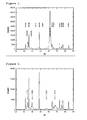
- the X-ray diffraction patterns (CuK ⁇ radiation, ⁇ -2 ⁇ geometry) of the as-deposited NbN and Nb 0.29 Zr 0.71 N layers are shown in Figure 1 and Figure 2 respectively. Apart from the peaks corresponding to the WC-Co substrates, there are few similarities between the patterns of the NbN and Nb 0.29 Zr 0.71 N samples.
- the as-deposited layer of Nb 0.29 Zr 0.71 N, Figure 2 consists of a NaCl type structure as seen by the identification of the (111), (200), (220), and (311) peaks. However, the XRD pattern of NbN is completely different.
- the texture defined as the ratio (K) between the area of the h-(Me1,Me2)X (100) peak and the h-(Me1,Me2)X (110) plus (103) peaks is for the NbN sample 0.12.
- the FWHM of the h-NbN (110) plus (103) peaks is 1.2°2 ⁇ and of the h-NbN (100) peak 0.7°2 ⁇ .
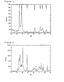
- Phase identification of the NbN in as-deposited condition was made by X-ray diffraction using a constant gracing incident angle of 1° between primary beam and sample surface and scanning the detector in order to magnify peaks originating from the coating , see Figure 3.
- the presence of h-NbN is confirmed by the indexing of the diffraction pattern in the anti-NiAs type structure.
- the peak-to-background ratio for the h-(Nb,Zr)N (110) plus (103) peaks is 153 (A), 92 (B), 109 (C), 79 (D), and 4.5 (E), respectively.
- the hardness and Young's modulus of the Nb-Zr-N layers were measured by nanoindentation using a Nano IndentedTM II instrument on polished tapered cross-sections using maximum load of 25 mN resulting in a maximum penetration depth of about 200 nm.
- the hardness and Young's modulus values are reported in Table 1. It can clearly be seen from Table 1 that the hardness increases drastically when h-(Nb,Zr)N is present in the layer.
- Cemented carbide exchangeable end mills of type MM12-12012-B90P-M05 with composition 90 wt-% WC - 10 wt-% Co (WC grain size 0.8 ⁇ m) were coated using similar deposition conditions as in Example 1 (the name of the variants in Example 2 refers to variant names in Example 1 with similar composition).
- a fixture with three-fold rotation was used.
- the end mills were positioned at different levels in order to get different composition.
- the deposition period was adjusted from example 1 to 140 min in order to get 3.0 ⁇ m on the flank face.
- TiN TiN coated end mill of the same geometry and substrate was used, here called TiN.
- the layer thickness on the flank face on this variant was 1.4 ⁇ m.
- a semi-finishing copy milling test was performed using the following cutting data:
- Vbmax was measured at two different positions (at the top and 1 mm from the top), see Table 2. Table 2. Variant Vb max [mm] At the top Vb max [mm] 1 mm from the top C 0.20 0.12 E 0.47 0.28 I 0.68 0.24 TiN 0.82 0.18
- variants with high amount of h-(Nb,Zr)N as variant A (single phase h-NbN) and C, have the longest tool life.
Abstract
Description
- The present invention relates to a cutting tool for machining by chip removal consisting of a substrate of cemented carbide, cermet, ceramics, cubic boron nitride based material, or high speed steel, and a hard and wear resistant refractory coating of which at least one layer comprises a hexagonal MeX-phase formed in-situ during the deposition either as a single phase or by co-deposition together with a second phase. This finding can be used in several ways giving a high degree of possibilities to tailoring the properties of the finished tool, for example as hexagonal structure particles in a coating matrix of another type, or of the same type, of crystal structure, or as separate layers within a multilayer superstructure. Since the hexagonal type of structure has different mechanical and chemical properties than for instance a cubic structure, the combination of different types of crystallites can give completely new properties compared to a single structure material.
- The majority of all PVD-layers used today for metal cutting for machining by chip removal consists of crystalline TiN, Ti(C,N), and (Ti,A1)N with a cubic NaCl type structure. However, a metastable (Ti,Al)N layer will at elevated temperature, during heat treatment or at service if sufficient amount of energy is supplied, phase separate into c-TiN and h-AIN. These precipitates of a h-AIN and/or c-AIN can act as hardeners in the layers. It has been demonstrated that an optimised amount of precipitates of c-AIN and/or h-AIN in a cubic c-(Ti,AI)N matrix will improve the performance of the layer as disclosed by
EP-A-1400609 andEP-A-1452621 . However, the volume occupied per atom in the hexagonal (wurtzite type) structure is 25% larger than in the cubic structure (NaCl type). Therefore, if the degree of structural transformation of an applied (Ti,AI)N layer proceeds too far this may lead to cohesive failure and accelerated wear of the layer. - It is an object of the present invention to provide a coating comprising at least one layer containing a h-MeX phase to be applied to a cutting tool for machining by chip removal.
- It is a further object of the present invention to provide a method for depositing layers comprising an h-MeX phase using PVD technology.
- It has been found that, by balancing the chemical composition, the amount of thermal energy and the degree of ion induced surface activation during growth, growth rate, and pressure, layers containing h-MeX phase can be obtained which compared to the prior art display enhanced performance in metal cutting. The layers comprise crystals of h-MeX with or without the co-existence of c-NaCl type structures of nitrides and/or carbides and/or oxides. The layers are deposited using PVD-technique, preferably by arc evaporation.
-
- Figure 1. X-ray diffraction pattern using CuKα radiation and θ-2θ geometry obtained from a h-NbN-layer, according to the invention, in the as-deposited condition.
- Figure 2. X-ray diffraction pattern using CuKα radiation and θ-2θ geometry obtained from a (Nb,Zr)N-layer with atomic ratio of Nb/Zr = 29/71 in as-deposited condition.
- Figure 3. X-ray diffraction pattern using CuKα radiation and a constant gracing incident angle of 1 between primary beam and sample surface and by scanning only the detector from a NbN-layer, according to the invention, in as-deposited condition.
- Figure 4. X-ray diffraction pattern using CuKα radiation and θ-2θ geometry obtained from a (Nb,Zr)N-layer, according to the invention, with atomic ratio of Nb/Zr = 86/14 in as-deposited condition.
- According to the present invention, a cutting tool for machining by chip removal is provided comprising a body of a hard alloy of cemented carbide, cermet, ceramics, cubic boron nitride based material, or high speed steel, onto which a wear resistant coating is deposited composed of one or more layers of refractory compounds comprising at least one layer being composed of crystals of h-MeX phase. Additional layers are composed of nitrides and/or carbides and/or oxides with the elements chosen from Ti, Zr, Hf, V, Nb, Ta, Cr, Mo, W, Si and Al, grown using physical vapour deposition (PVD), or other deposition technologies such as plasma enhanced chemical vapour deposition (PACVD) and/or chemical vapour deposition (CVD). Tools according to the present invention are particularly useful in metal cutting applications where the chip thickness is small and the work material is hard such as copy milling using solid end mills, insert milling cutters or drilling of hardened steels.
- The h-MeX layer(s) comprise(s) crystals of h-MeX phase. The composition shall be described as Me1aMe21-aXb where Me1 is one or more of the elements V, Cr, Nb, and Ta and Me2 is one or more of the elements Ti, Zr, Hf, Al, and Si and a > 0.5 and X one or more of the elements N, C, O and B. The non-metal to metal atomic ratio, here defined as R = (at-% X)/(at-% Me1 + at-% Me2) of the h-(Me1,Me2)X phase, is between 0.5 and 1.0, preferably between 0.75 and 1.0.
- The h-MeX layer comprising h-(Me1,Me2)X phase is characterised by:
- The existence of a crystalline hexagonal phase, h-(Me1,Me2)X, as detected by X-ray diffraction (XRD) in θ-2θ and/or gracing incidence geometry showing one or more of the following features:
- a h-(Me1,Me2)X (100) peak, in case of h-NbN using CuKα radiation at about 35 °2θ,
- a h-(Me1,Me2)X (101) peak, in case of h-NbN using CuKα radiation at about 39 °2θ,
- a h-(Me1,Me2)X (102) peak, in case of h-NbN using CuKα radiation at about 48 °2θ,
- a h-(Me1,Me2)X (110) peak, in the case of h-NbN using CuKα radiation at about 62 °2θ,
- a h-(Me1,Me2)X (103) peak, in the case of h-NbN using CuKα radiation at about 62 °2θ,
- a h-(Me1,Me2)X (112) peak, in case of h-NbN using CuKα radiation at about 72 °2θ,
- a h-(Me1,Me2)X (201) peak, in case of h-NbN using CuKα radiation at about 75 °2θ,
- a h-(Me1,Me2)X (202) peak, in the case of h-NbN using CuKα radiation at about 83 °2θ.
- When Me and X are not Nb and N, respectively, the peak positions could be shifted.
- The structure of the h-(Me1,Me2)X is preferably of anti-NiAs type.
- The ratio, L, between the area of the h-(Me1,Me2)X (110) plus (103) peaks (= A(h-(Me1,Me2)X100+103) and the c-(Me1,Me2)X (200) peak (= A(c-(Me1,Me2)X200), i.e. L = A(h-Me1Me2X110+103)/ A(C-MeX200) in the X-ray diffraction pattern, in θ-2θ geometry, from said layer, is larger than 0.1, preferably larger than 0.2, and/or that the peak-to-background ratio for the h-(Me1,Me2)X (110) plus (103) peaks is larger than 2, preferably larger than 4.
- The texture defined as the ratio, K, between the area of the h-(Me1,Me2)X (100) peak, using CuKα radiation in θ-2θ geometry, and the h-(Me1,Me2)X (110) plus (103) peaks is between 0 and 0.5 and preferably between 0.0 and 0.25.
- The FWHM (Full Width Half Maximum) value, using CuKα radiation in θ-2θ geometry, caused by small grains and/or inhomogeneous stresses, of the:
- h-(Me1,Me2)X (110) plus (103) peaks is between 0.5 and 3.0 °2θ and/or
- h-(Me1,Me2)X (100) peak is between 0.4 and 2.5 °2θ.
- X consists of less than 30 at-% O and/or B with balance of N and/or C.
- The layer comprising h-(Me1,Me2)X has a considerably increased hardness compared to a cubic single phase layer of a NaCl type c-MeX structure, see Example 1, as demonstrated by the system of h-(Nb,Zr)N and c-(Nb,Zr)N.
- The total coating thickness, if the h-(Me1,Me2)X containing layer(s) according to the present invention are combined with other layer(s), is between 0.1 and 15 µm, preferably between 0.5 and 12 µm with the total thickness of the non h-(Me1,Me2)X containing layer(s) varying between 0.5 and 10 µm.
- In another alternative embodiment the h-(Me1,Me2)X containing layer(s) of 0.5 and 12 µm thickness, with or without other layer(s) according to the above described, an outer 0.5 to 5 µm thick layer consisting of a solid low friction material based on MoS2, DLC(Diamond Like Coating) or a MeC/C, where Me is Cr, W, Ti or Ta, can be deposited on top of the coating.
- In yet another alternative embodiment the h-(Me1,Me2)X containing layer(s), between 0.1 and 2 µm thickness, are one of one to five different materials in a 1.0 to 15 µm thick multilayer coating consisting of individually 2-500, preferably 5-200, layers.
- In yet another alternative embodiment the h-(Me1,Me2)X containing layer(s) of 0.5 and 20 µm thickness can be deposited on top of a CVD coating which may comprise one or more layer(s) of crystalline Al2O3.
- In yet another alternative embodiment at least one h-(Me1,Me2)X containing layer(s) of 0.1 and 1.0 µm thickness is used for metal cutting application where the chip thickness is very small.
- The method used to grow the layers, comprising h-(Me1,Me2)X phase of the present invention, here exemplified by the system Nb-Zr-N, is based on arc evaporation of an alloyed, or composite cathode, under the following conditions:
- The Nb-Zr cathode composition is >70 at-% Nb, preferably >80 at-% Nb and balance of Zr.
- The evaporation current is between 50 A and 200 A depending on cathode size and cathode material. When using cathodes of 63 mm in diameter the evaporation current is preferably between 70 A and 140 A.
- The substrate bias is between -10 V and -300 V, preferably between -40 V and -120 V.
- The deposition temperature is between 400°C and 700°C, preferably between 500°C and 700°C.
- If pure Nb and/or Zr cathodes are used the evaporation current is preferably between 80 A and 140 A for Nb and between 60 A and 100 A for Zr. In order to get the correct composition of the layer, working with pure single element cathodes, the arc current and the number of cathodes per element has to be optimised properly. By using twice as many Nb cathodes as Zr cathodes, and/or a higher arc current on the Nb cathodes, the correct layer composition and structure in the Nb-Zr system can be achieved.
- When growing layer(s) containing h-(Me1,Me2)X an Ar+N2 atmosphere consisting of 0-50 vol-% Ar, preferably 0-20 vol-%, at a total pressure of 0.5 Pa to 9.0 Pa, preferably 1.5 Pa to 5.0 Pa, is used.
- For the growth of h-(Me1,Me2)X layer(s) where X includes C and O, carbon and/or oxygen containing gases have to be added to the N2 and/or Ar+N2 atmosphere (e.g. C2H2, CH4, CO, CO2, O2). If X also includes boron it could be added either by alloying the target with boron or by adding a boron containing gas to the atmosphere.
- In order to obtain one of the preferred structures according to the invention, namely a layer containing h-(Me1,Me2)X here exemplified by h-(Nb,Zr)N, it has been found that several deposition parameters should be defined. A significant factor is the ratio between the flux of Nb from the cathode and the N2 partial pressure, PN2 While the inventors are not to be bound by a particular theory, it is believed that the deposition rate, which is directly related to the Nb-flux, is rather low in the segment of rotational angle where the majority of deposition occurs. The deposition rate should not be too high, here below about 4 µm/h in one fold rotation, with two Nb cathodes separated by 180°, or about 1.5 µm/h at three fold rotation. The deposition rates given above, which actually are average values and not the key parameter, are to be seen as rough guidelines at a deposition temperature of 530°C. When using a higher deposition rate a higher deposition temperature will also be needed. For every deposition rate there is a lower limit for the PN2 of the process. A too low PN2 will give metallic Nb(N) and/or c-NbN in the layer. In the used system the best results are obtained for pressures higher than 0.5 Pa. Since one key factor is to keep the maximum deposition rate low, the minimum distance between cathode surface and substrate is important, preferably 150 mm or more. Here a distance below 130 mm seems to be too short.
- The deposition of layer(s) containing h-(Me1,Me2)X phase of the type described above could also be possible using V and/or Ta as Me1 due to similarities with Nb. Using Ti, Zr, and Hf, as Me2, as alloying elements should also be valid using a maximum alloying content preferably less than 20 at-%, most preferably less than 15 at-%, of the total metal content, based on reported hardness versus composition values in Table 1 for the Nb-Zr-N system. Examples on this alloying route is h-(V,Nb,Ta)N, h-(V,Nb,Ta)1-x(Ti,Zr,Hf)xN with x preferably <0.2 and most preferably <0.15.
- In order to get good high temperature oxidation resistance nitrides are preferred compared to carbonitrides and carbides. Additionally improved oxidation resistance could be achieved by alloying with one or more of the Ti, Al and Si as Me2-elements and Cr as an M1-element. These alloying elements could be present in the h-(Me1,Me2)X phase as well in a second phase, which could be of c-NaCI type.
- When growing layer(s) containing h-(Me1,Me2)X phase there is a risk that the compressive residual stress becomes very high, up to the level of 3-8 GPa corresponding to a strain of 0.5% to 1.5% (of the h-MeX phase), which will influence the performance negatively in cutting applications when sharp cutting edges are used and/or when the demand on good adhesion is of utmost importance. One possibility to decrease the compressive residual stresses is to apply a post annealing process, or in-situ annealing, preferably in an atmosphere of Ar and/or N2 at temperatures between 600°C and 1100°C for a period of 20 to 600 min.
- The present invention has been described with reference to layer(s) containing h-(Me1,Me2)X phase deposited using arc evaporation. It is to be understood that h-(Me1,Me2)X phase containing layer(s) also could be produced using other PVD-technologies such as magnetron sputtering, electron beam evaporation, ion plating or laser ablation.
- Polished cemented carbide substrates with composition 93.5 wt-% WC - 6 wt-% Co - 0.5 wt-% (Ta,Nb)C were used. The WC grain size was about 1 µm and the hardness was 1630 HTV10.
- Before deposition, the substrates were cleaned in ultrasonic baths using alkali solution and alcohol and subsequently placed in the PVD-system using a fixture of one-fold rotation. The shortest cathode-to-substrate distance was 160 mm. The system was evacuated to a pressure of less than 2.0×10⁻³ Pa, after which the substrates were sputter cleaned with Ar ions. The layers were grown using arc evaporation of Nb and Zr cathodes (63 mm in diameter) mounted so a vertical metal composition gradient varied from Nb0.97Zr0.03 to Nb0.29Zr0.71 (measured by EDS). The nitrogen content (measured by EDS) of the variants containing h-AlN was between (Nb,Zr)N0,77-0.92. This means that the ratio R = (at-% X)/(at-% Me1 + at-% Me2) is between 0.77 and 0.92 where X is N and Me1 is Nb and Me2 is Zr.
- The deposition was carried out in a 99.995% pure N2 atmosphere at a total pressure of 3.0 Pa, using a substrate bias of-110 V for 60 minutes. The layer thickness was about 3.5 µm. The deposition temperature was about 530°C. Immediately after deposition the chamber was vented with dry N2.
- The NbN layer was grown using a separate deposition experiment, using the same deposition data as above except that only pure elemental Nb cathodes were used.
- The X-ray diffraction patterns (CuKα radiation, θ-2θ geometry) of the as-deposited NbN and Nb0.29Zr0.71N layers are shown in Figure 1 and Figure 2 respectively. Apart from the peaks corresponding to the WC-Co substrates, there are few similarities between the patterns of the NbN and Nb0.29Zr0.71N samples. The as-deposited layer of Nb0.29Zr0.71N, Figure 2, consists of a NaCl type structure as seen by the identification of the (111), (200), (220), and (311) peaks. However, the XRD pattern of NbN is completely different. Especially, the absence of the cubic NaCl type structure and the occurrence of a large peak at 62 °2θ (FWHM = 1.2 °2θ) and a peak at 38 °2θ (FWHM = 1.3 °2θ), both of which are not seen in Nb0.29Zr0.71N. Further, there is a slight increase in intensity going from 70 to 75 °2θ in NbN, while there is a decrease in intensity in the same region for Nb0.29Zr0.71N. Also, there is a clear difference in peak position of the peak at 34.5 °2θ in Nb0.29Zr0.71N compared to the peak at 34.0 °2θ for NbN layer. The texture, defined as the ratio (K) between the area of the h-(Me1,Me2)X (100) peak and the h-(Me1,Me2)X (110) plus (103) peaks is for the NbN sample 0.12. The FWHM of the h-NbN (110) plus (103) peaks is 1.2°2θ and of the h-NbN (100) peak 0.7°2θ.
- Phase identification of the NbN in as-deposited condition was made by X-ray diffraction using a constant gracing incident angle of 1° between primary beam and sample surface and scanning the detector in order to magnify peaks originating from the coating , see Figure 3. The presence of h-NbN is confirmed by the indexing of the diffraction pattern in the anti-NiAs type structure. At increasing Zr content the amount of c-(Nb,Zr)N (NaCl-type structure) increases. Figure 4 shows an X-ray pattern from a layer with atomic ratio of Nb/Zr = 86/14 (sample E) in as-deposited condition. The ratio, L, between the area of the h-(Me1,Me2)X (110) peak at about 62 °2θ (= A(h-(Me1,Me2)X)110) and the c-(Me1,Me2)X (200) peak at about 41 °2θ (= A(c-(Me1,Me2)X)200), i.e. L = A(h-(Nb,Zr)N)110)/ A(c-(Nb,Zr)N)200) is for this sample 0.25.
- For selected samples found in Table 1, the peak-to-background ratio for the h-(Nb,Zr)N (110) plus (103) peaks is 153 (A), 92 (B), 109 (C), 79 (D), and 4.5 (E), respectively.
- The hardness and Young's modulus of the Nb-Zr-N layers were measured by nanoindentation using a Nano Indented™ II instrument on polished tapered cross-sections using maximum load of 25 mN resulting in a maximum penetration depth of about 200 nm. The hardness and Young's modulus values are reported in Table 1. It can clearly be seen from Table 1 that the hardness increases drastically when h-(Nb,Zr)N is present in the layer. The layer with Nb/Zr = 86/14, variant E, has an hardness in-between the level of the h-(Nb,Zr)N, around 43-48 GPa, and the c-(Nb,Zr)N layers around 33 GPa.
Table 1. Variant Nb/Zr (at-%) Hardness (GPa) Young's Modulus (GPa) Phases detected FWHM h-(100) °2θ FWHM h-(110) plus h-(103) °2θ Res. Strain (%) Texture parameter K A 100/0 h-NbN, a=2.98, c=5.49 0.7 1.2 0.12 B 97/3 47 595 h-NbN, a=3.00, c=5.49 c-(Nb,Zr)N a=4.44 0.8 1.5 -1.6 0.12 C 95/5 43 578 h-NbN, a=2.98, c=5.53 c-(Nb,Zr)N a=4.44 0.8 1.5 0.11 D 93/7 48 597 h-NbN, a=3.00, c=5.49 c-(Nb,Zr)N a=4.45 0.8 1.6 -1.7 0.19 E 86/14 38 8 493 h-NbN, a=3.01, c=5.50 c-(Nb,Zr)N a=4.443 0.8 2.2 0.52 F 75/25 33 474 c-(Nb,Zr)N a=4.47 G 57/43 33 473 c-(Nb,Zr)N a=4.50 H 43/57 33 497 c-(Nb,Zr)N a=4.53 -0.9 I 33/67 33 491 c-(Nb,Zr)N a=4.55 J 29/71 33 515 c-(Nb,Zr)N a=4.55 -0.6 - Cemented carbide exchangeable end mills of type MM12-12012-B90P-M05 with
composition 90 wt-% WC - 10 wt-% Co (WC grain size 0.8 µm) were coated using similar deposition conditions as in Example 1 (the name of the variants in Example 2 refers to variant names in Example 1 with similar composition). A fixture with three-fold rotation was used. The end mills were positioned at different levels in order to get different composition. The deposition period was adjusted from example 1 to 140 min in order to get 3.0 µm on the flank face. As a reference a TiN coated end mill of the same geometry and substrate was used, here called TiN. The layer thickness on the flank face on this variant was 1.4 µm. - A semi-finishing copy milling test was performed using the following cutting data:
- Material: DIN X100CrMoV 5 1, 59HRC
- n = 4050 rpm
- ap = ae = 0.9 mm
- vf = 900 mm/min
- hm = 0.015 mm
- After 30 min in cut the maximum flank wear, Vbmax, was measured at two different positions (at the top and 1 mm from the top), see Table 2.
Table 2. Variant Vb max [mm] At the top Vb max [mm] 1 mm from the top C 0.20 0.12 E 0.47 0.28 I 0.68 0.24 TiN 0.82 0.18 - This copy milling test shows that the variant C (this invention) has the lowest wear rate followed by the variant E with a structure mixed between the h-(Nb,Zr)N and c-(Nb,Zr)N.
- A copy milling test using RDHW10T3M0T-MD06 inserts coated similarly as in Example 1 (variants A, C and E). The tool life was measured when the inserts were worn out as defined as when sparkles were created and the material got an uneven surface. Tool life is reported in table 3.
- Material: DIN X 155 CrMoV 12 l, hardened to 58HRC
- Dry machining
- Vc = 250 m/min
- fz = 0,2 mm/tooth
- ap = 1 mm, ae 2 mm
- In this test the variants with high amount of h-(Nb,Zr)N, as variant A (single phase h-NbN) and C, have the longest tool life.
| Table 3. | ||
| Variant | Tool life Edge 1(min) | Tool life Edge 2 (min) |
| A | 5.2 | 4.5 |
| C | 4.3 | 5.4 |
| E | 2.5 | 2.8 |
| TiN | 3.1 | 2.5 |
Claims (7)
- Cutting tool insert, solid end mill, or drill, comprising a substrate and a coating composed of one or more layers of refractory compounds of which characterised in that at least one layer comprises crystalline hexagonal phase, h-(Me1, Me2)X, described with the composition Me1aMe21-aXb where Me1 is one or more of the elements V, Cr, Nb, and Ta and Me2 is one or more of the elements Ti, Zr, Hf, Al, and Si and a > 0.5 and X one or more of the elements N, C, O and B, the ratio R = (at-% X)/(at-% Me1 + at-% Me2) of the Me1aMe21-aXb phase is between 0.5 and 1.0, preferably between 0.75 and 1.0, and that X contains less than 30 at-% of O + B, the X-ray diffraction (XRD) pattern in θ-2θ and/or gracing incidence geometry from the crystalline hexagonal phase, h-(Me1,Me2)X, showing one or more of the following peaks:- a h-(Me1,Me2)X (100) peak- a h-(Me1,Me2)X (101) peak- a h-(Me1,Me2)X (102) peak- a h-(Me1,Me2)X (110) peak- a h-(Me1,Me2)X (103) peak- a h-(Me1,Me2)X (112) peak- a h-(Me1,Me2)X (201) peak- a h-(Me1,Me2)X (202) peak.
- Cutting tool according to claim 1 characterised in that the ratio, L, between the area of the h-(Me1,Me2)X (110) plus (103) peaks (= A(h-(Me1,Me2)X110+103) and the c-(Me1,Me2)X (200) peak (= A(c-(Me 1,Me2)X200), i.e. L = A(h-Me1Me2X110+103)/ A(c-MeX200) in the X-ray diffraction pattern, in θ-2θ geometry, from said layer, is larger than 0.1, preferably larger than 0.2, and/or that the peak-to-background ratio for the h-(Me1,Me2)X (110) plus (103) peaks is larger than 2, preferably larger than 4.
- Cutting tool insert according to claim 1 characterised in that Me1 is one or more of the elements V, Cr, Nb or Ta and Me2 is one or more of the elements Ti, Zr, Hf, Al, or Si.
- Cutting tool insert according to claim 1 characterised in that the texture here defined as the ratio, K, between the area of the h-(Me1,Me2)X (100) peak and the h-(Me1,Me2)X (110) plus (103) peaks in the X-ray diffraction pattern, in θ-2θ geometry, from said layer is between 0 and 0.5 and preferably between 0.0 and 0.25.
- Cutting tool insert according to claim 1 characterised in that the FWHM (Full Width Half Maximum) value of the h-(Me1,Me2)X (110) plus (103) peaks in the X-ray diffraction pattern, in θ-2θ geometry, from said coating is between 0.5 and 3.0 °2θ and/or h-(Me1,Me2)X (100) peak is between 0.4 and 2.5 °2θ.
- Cutting tool insert according to claim 1 characterised in that the structure of the h-(Me1,Me2)X is of anti-NiAs type.
- Method of producing a coated cutting tool insert, solid end mill, or drill, comprising a substrate and a coating characterised in that the coating is composed of one or more layers of refractory compounds of which at least one layer comprises a h-(Me1,Me2)X phase described with the composition Me1aMe21-aXb where Me1 is one or more of the elements V, Cr, Nb, and Ta and Me2 is one or more of of the elements Ti, Zr, Hf, Al, and Si and a > 0.5 and X one or more of the elements N, C, O and B and that the ratio R = (at-% X)/(at-% Me1 + at-% Me2) of the Me1aMe21-aXb phase, is between 0.5 and 1.0, preferably between 0.75 and 1.0 and that X contains less than 30 at-% of O + B.
Applications Claiming Priority (1)
| Application Number | Priority Date | Filing Date | Title |
|---|---|---|---|
| SE0501038A SE529223C2 (en) | 2005-05-06 | 2005-05-06 | Coated cutting tool comprising hexagonal h- (Mel, Me2) X phase |
Publications (2)
| Publication Number | Publication Date |
|---|---|
| EP1722009A1 true EP1722009A1 (en) | 2006-11-15 |
| EP1722009B1 EP1722009B1 (en) | 2008-10-01 |
Family
ID=36716909
Family Applications (1)
| Application Number | Title | Priority Date | Filing Date |
|---|---|---|---|
| EP06445019A Not-in-force EP1722009B1 (en) | 2005-05-06 | 2006-04-28 | Thin wear resistant coating |
Country Status (8)
| Country | Link |
|---|---|
| US (1) | US8507108B2 (en) |
| EP (1) | EP1722009B1 (en) |
| JP (1) | JP2006312235A (en) |
| KR (1) | KR100858855B1 (en) |
| CN (1) | CN100525968C (en) |
| AT (1) | ATE409758T1 (en) |
| DE (1) | DE602006002920D1 (en) |
| SE (1) | SE529223C2 (en) |
Cited By (14)
| Publication number | Priority date | Publication date | Assignee | Title |
|---|---|---|---|---|
| EP2201152A1 (en) * | 2007-09-14 | 2010-06-30 | Seco Tools Ab | Coated cutting insert for machining of titanium based alloys |
| US8389115B2 (en) | 2008-03-07 | 2013-03-05 | Seco Tools Ab | Thermally stabilized (Ti,Si)N layer for cutting tool insert |
| EP2679704A1 (en) | 2012-06-29 | 2014-01-01 | Seco Tools Ab | Coated cutting insert |
| WO2014037104A1 (en) | 2012-09-08 | 2014-03-13 | Oerlikon Trading Ag, Trübbach | Ti-al-ta-based coating exhibiting enhanced thermal stability |
| RU2545941C2 (en) * | 2013-07-23 | 2015-04-10 | Федеральное государственное бюджетное образовательное учреждение высшего профессионального образования "Ульяновский государственный технический университет" | Method of producing wear resistant coating for cutting tool |
| RU2548862C2 (en) * | 2013-07-12 | 2015-04-20 | Федеральное государственное бюджетное образовательное учреждение высшего профессионального образования "Ульяновский государственный технический университет" | Method of wear-resistant coating obtainment for cutting tool |
| RU2548858C2 (en) * | 2013-07-23 | 2015-04-20 | Федеральное государственное бюджетное образовательное учреждение высшего профессионального образования "Ульяновский государственный технический университет" | Method of producing wear resistant coating for cutting tool |
| RU170600U1 (en) * | 2016-06-01 | 2017-05-02 | Общество с ограниченной ответственностью "Сборные конструкции инструмента, фрезы Москвитина" | END MILL |
| RU2620530C1 (en) * | 2015-12-15 | 2017-05-26 | федеральное государственное бюджетное образовательное учреждение высшего образования "Ульяновский государственный технический университет" | Method of producing sandwiched coating for cutting tool |
| RU2622530C1 (en) * | 2015-12-15 | 2017-06-16 | федеральное государственное бюджетное образовательное учреждение высшего образования "Ульяновский государственный технический университет" (УлГТУ) | Method of producing sandwiched coating for cutting tool |
| RU2622532C1 (en) * | 2015-12-15 | 2017-06-16 | федеральное государственное бюджетное образовательное учреждение высшего образования "Ульяновский государственный технический университет" | Method of producing sandwiched coating for cutting tool |
| RU2627317C1 (en) * | 2016-06-06 | 2017-08-07 | Общество с ограниченной ответственностью "Сборные конструкции инструмента, фрезы Москвитина" | End cutter |
| WO2018215558A1 (en) | 2017-05-23 | 2018-11-29 | Oerlikon Surface Solutions Ag, Pfäffikon | Thick TiAlTaN/AlCrN multilayer coating films on turbine components |
| EP3396015A4 (en) * | 2016-03-18 | 2019-09-11 | Northeastern University | Composite functional cutter coating for cutting titanium alloy and preparation method therefor |
Families Citing this family (17)
| Publication number | Priority date | Publication date | Assignee | Title |
|---|---|---|---|---|
| JP4774080B2 (en) * | 2007-08-02 | 2011-09-14 | 株式会社神戸製鋼所 | Hard coating material and cold plastic working mold |
| CN101210310B (en) * | 2007-12-21 | 2010-12-08 | 广州有色金属研究院 | Multi-component multi-layer hard thin film material for minitype drill bit surface modification and preparation method thereof |
| JP5234931B2 (en) * | 2008-06-23 | 2013-07-10 | 株式会社神戸製鋼所 | Hard coating member and molding tool |
| WO2010052184A2 (en) * | 2008-11-04 | 2010-05-14 | Oerlikon Trading Ag, Trübbach | Wear protection layer and method for the manufacture thereof |
| US8956722B2 (en) * | 2009-02-27 | 2015-02-17 | Oerlikon Metaplas Gmbh | Layer system for the formation of a surface layer on a surface of a substrate and coating method for the manufacture of a layer system |
| DE102009001675A1 (en) * | 2009-03-19 | 2010-09-23 | Eberhard-Karls-Universität Tübingen | cutting tool |
| EP2463398B1 (en) * | 2009-08-04 | 2018-04-04 | Tungaloy Corporation | Coated member |
| CN102294854B (en) * | 2010-06-24 | 2014-07-09 | 鸿富锦精密工业(深圳)有限公司 | Hard coating and preparation method thereof and covering element having hard coating |
| TWI547379B (en) * | 2010-12-21 | 2016-09-01 | 鴻海精密工業股份有限公司 | A multilayer article with brass layer and stacked silicon carbide ceramic layer, and the method for manufacturing same |
| US9132484B2 (en) * | 2011-08-29 | 2015-09-15 | Kyocera Corporation | Cutting tool |
| CN104703734B (en) * | 2012-10-01 | 2016-08-24 | 日立工具股份有限公司 | Hard film-coated tool and manufacture method thereof |
| DE102013104254A1 (en) | 2013-04-26 | 2014-10-30 | Walter Ag | Tool with CVD coating |
| RU2538057C1 (en) * | 2013-07-12 | 2015-01-10 | Федеральное государственное бюджетное образовательное учреждение высшего профессионального образования "Ульяновский государственный технический университет" | Method for obtaining multi-layered coating for cutting tool |
| CN103586520B (en) * | 2013-10-17 | 2016-01-27 | 厦门金鹭特种合金有限公司 | A kind of coated cemented carbide endmill and preparation method thereof |
| DE102013018007A1 (en) * | 2013-11-29 | 2015-06-03 | Oerlikon Trading Ag, Trübbach | Method for improving the Gegenkörperverschleisses in tribological contact |
| CN106573313B (en) * | 2014-07-25 | 2018-10-09 | 株式会社泰珂洛 | Coated cutting tool |
| RU2715267C2 (en) * | 2015-12-22 | 2020-02-26 | Сандвик Интеллекчуал Проперти Аб | Cutting tool with coating and method |
Citations (6)
| Publication number | Priority date | Publication date | Assignee | Title |
|---|---|---|---|---|
| JPH04128363A (en) * | 1990-09-19 | 1992-04-28 | Limes:Kk | Composite material |
| EP1174528A2 (en) * | 2000-07-13 | 2002-01-23 | Hitachi Tool Engineering Ltd. | Multilayer-coated cutting tool |
| EP1219723A2 (en) * | 2000-12-28 | 2002-07-03 | Kabushiki Kaisha Kobe Seiko Sho | Hard film for cutting tools |
| EP1378304A2 (en) * | 2002-07-01 | 2004-01-07 | Seco Tools Ab | Wear resistant coating with enhanced toughness |
| EP1400609A1 (en) * | 2002-09-04 | 2004-03-24 | Seco Tools Ab | Precipitation hardened wear resistant coating |
| EP1452621A2 (en) * | 2002-09-04 | 2004-09-01 | Seco Tools Ab | Composite structured wear resistant coating |
Family Cites Families (11)
| Publication number | Priority date | Publication date | Assignee | Title |
|---|---|---|---|---|
| EP0701982B1 (en) * | 1994-09-16 | 2002-07-03 | Sumitomo Electric Industries, Limited | Layered film made of ultrafine particles and a hard composite material for tools possessing the film |
| JP3488526B2 (en) * | 1994-12-14 | 2004-01-19 | 三菱マテリアル神戸ツールズ株式会社 | Hard coatings and hard coatings with excellent wear resistance |
| JP4171099B2 (en) * | 1998-04-24 | 2008-10-22 | 株式会社神戸製鋼所 | Hard film with excellent wear resistance |
| JP2000144376A (en) * | 1998-11-18 | 2000-05-26 | Sumitomo Electric Ind Ltd | Film excellent in sliding characteristic |
| JP3404003B2 (en) * | 2000-05-23 | 2003-05-06 | 日立ツール株式会社 | Coated cutting tool |
| SE0004203D0 (en) * | 2000-11-16 | 2000-11-16 | Haakan Hugosson | A surface coating |
| DE10233222B4 (en) * | 2001-07-23 | 2007-03-01 | Kabushiki Kaisha Kobe Seiko Sho (Kobe Steel, Ltd.), Kobe | Hard wear-resistant layer, method of forming same and use |
| DE10242421A1 (en) * | 2002-09-06 | 2004-03-18 | Fenker, Martin, Dr. | Coating for substrates used in the automobile industry comprises niobium nitride or niobium metal nitride |
| JP4240983B2 (en) | 2002-10-07 | 2009-03-18 | 沖電気工業株式会社 | How to set the input pin capacitance |
| JP2004314185A (en) * | 2003-04-11 | 2004-11-11 | Hitachi Tool Engineering Ltd | Coated carbide drill |
| US7226670B2 (en) * | 2003-04-28 | 2007-06-05 | Oc Oerlikon Balzers Ag | Work piece with a hard film of AlCr-containing material, and process for its production |
-
2005
- 2005-05-06 SE SE0501038A patent/SE529223C2/en not_active IP Right Cessation
-
2006
- 2006-04-28 EP EP06445019A patent/EP1722009B1/en not_active Not-in-force
- 2006-04-28 AT AT06445019T patent/ATE409758T1/en active
- 2006-04-28 DE DE602006002920T patent/DE602006002920D1/en active Active
- 2006-05-04 KR KR1020060040671A patent/KR100858855B1/en not_active IP Right Cessation
- 2006-05-08 US US11/429,450 patent/US8507108B2/en not_active Expired - Fee Related
- 2006-05-08 CN CNB2006100794675A patent/CN100525968C/en not_active Expired - Fee Related
- 2006-05-08 JP JP2006129492A patent/JP2006312235A/en active Pending
Patent Citations (6)
| Publication number | Priority date | Publication date | Assignee | Title |
|---|---|---|---|---|
| JPH04128363A (en) * | 1990-09-19 | 1992-04-28 | Limes:Kk | Composite material |
| EP1174528A2 (en) * | 2000-07-13 | 2002-01-23 | Hitachi Tool Engineering Ltd. | Multilayer-coated cutting tool |
| EP1219723A2 (en) * | 2000-12-28 | 2002-07-03 | Kabushiki Kaisha Kobe Seiko Sho | Hard film for cutting tools |
| EP1378304A2 (en) * | 2002-07-01 | 2004-01-07 | Seco Tools Ab | Wear resistant coating with enhanced toughness |
| EP1400609A1 (en) * | 2002-09-04 | 2004-03-24 | Seco Tools Ab | Precipitation hardened wear resistant coating |
| EP1452621A2 (en) * | 2002-09-04 | 2004-09-01 | Seco Tools Ab | Composite structured wear resistant coating |
Non-Patent Citations (4)
| Title |
|---|
| KNOTEK O ET AL: "THE STRUCTURE AND COMPOSITION OF TI-ZR-N, TI-AI-ZR-N AND TI-AI-V-N COATINGS", MATERIALS SCIENCE AND ENGINEERING A: STRUCTURAL MATERIALS: PROPERTIES, MICROSTRUCTURE & PROCESSING, LAUSANNE, CH, vol. A105/106, January 1988 (1988-01-01), pages 481 - 488, XP000108123, ISSN: 0921-5093 * |
| KUTSCHEJ ET AL: "Comparative study of Ti1-xAlxN coatings alloyed with Hf, Nb, and B", SURFACE AND COATINGS TECHNOLOGY, ELSEVIER, AMSTERDAM, NL, vol. 200, no. 1-4, 19 March 2005 (2005-03-19), pages 113 - 117, XP005063476, ISSN: 0257-8972 * |
| PATENT ABSTRACTS OF JAPAN vol. 016, no. 394 (C - 0976) 21 August 1992 (1992-08-21) * |
| ROOS J R ET AL: "INTERRELATIONSHIP BETWEEN PROCESSING, COATING PROPERTIES AND FUNCTIONAL PROPERTIES OF STEERED ARC PHYSICALLY VAPOUR DEPOSITED (TI,AL)N AND (TI,NB)N COATINGS", JOURNAL OF THE LESS-COMMON METALS, ELSEVIER-SEQUOIA S.A. LAUSANNE, CH, vol. 193 / 194, no. 1 / 2, 1 December 1990 (1990-12-01), pages 547 - 556, XP000168996 * |
Cited By (20)
| Publication number | Priority date | Publication date | Assignee | Title |
|---|---|---|---|---|
| EP2201152A4 (en) * | 2007-09-14 | 2012-01-04 | Seco Tools Ab | Coated cutting insert for machining of titanium based alloys |
| EP2201152A1 (en) * | 2007-09-14 | 2010-06-30 | Seco Tools Ab | Coated cutting insert for machining of titanium based alloys |
| US8389115B2 (en) | 2008-03-07 | 2013-03-05 | Seco Tools Ab | Thermally stabilized (Ti,Si)N layer for cutting tool insert |
| US9523145B2 (en) | 2012-06-29 | 2016-12-20 | Seco Tools Ab | Coated cutting insert |
| EP2679704A1 (en) | 2012-06-29 | 2014-01-01 | Seco Tools Ab | Coated cutting insert |
| WO2014001190A1 (en) * | 2012-06-29 | 2014-01-03 | Seco Tools Ab | Coated cutting insert |
| CN104508185A (en) * | 2012-06-29 | 2015-04-08 | 山高刀具公司 | Coated cutting insert |
| CN104508185B (en) * | 2012-06-29 | 2018-06-15 | 山高刀具公司 | Coated cutting insert |
| WO2014037104A1 (en) | 2012-09-08 | 2014-03-13 | Oerlikon Trading Ag, Trübbach | Ti-al-ta-based coating exhibiting enhanced thermal stability |
| DE102012017731A1 (en) | 2012-09-08 | 2014-03-13 | Oerlikon Trading Ag, Trübbach | Ti-Al-Ta based coating with improved temperature resistance |
| RU2548862C2 (en) * | 2013-07-12 | 2015-04-20 | Федеральное государственное бюджетное образовательное учреждение высшего профессионального образования "Ульяновский государственный технический университет" | Method of wear-resistant coating obtainment for cutting tool |
| RU2548858C2 (en) * | 2013-07-23 | 2015-04-20 | Федеральное государственное бюджетное образовательное учреждение высшего профессионального образования "Ульяновский государственный технический университет" | Method of producing wear resistant coating for cutting tool |
| RU2545941C2 (en) * | 2013-07-23 | 2015-04-10 | Федеральное государственное бюджетное образовательное учреждение высшего профессионального образования "Ульяновский государственный технический университет" | Method of producing wear resistant coating for cutting tool |
| RU2620530C1 (en) * | 2015-12-15 | 2017-05-26 | федеральное государственное бюджетное образовательное учреждение высшего образования "Ульяновский государственный технический университет" | Method of producing sandwiched coating for cutting tool |
| RU2622530C1 (en) * | 2015-12-15 | 2017-06-16 | федеральное государственное бюджетное образовательное учреждение высшего образования "Ульяновский государственный технический университет" (УлГТУ) | Method of producing sandwiched coating for cutting tool |
| RU2622532C1 (en) * | 2015-12-15 | 2017-06-16 | федеральное государственное бюджетное образовательное учреждение высшего образования "Ульяновский государственный технический университет" | Method of producing sandwiched coating for cutting tool |
| EP3396015A4 (en) * | 2016-03-18 | 2019-09-11 | Northeastern University | Composite functional cutter coating for cutting titanium alloy and preparation method therefor |
| RU170600U1 (en) * | 2016-06-01 | 2017-05-02 | Общество с ограниченной ответственностью "Сборные конструкции инструмента, фрезы Москвитина" | END MILL |
| RU2627317C1 (en) * | 2016-06-06 | 2017-08-07 | Общество с ограниченной ответственностью "Сборные конструкции инструмента, фрезы Москвитина" | End cutter |
| WO2018215558A1 (en) | 2017-05-23 | 2018-11-29 | Oerlikon Surface Solutions Ag, Pfäffikon | Thick TiAlTaN/AlCrN multilayer coating films on turbine components |
Also Published As
| Publication number | Publication date |
|---|---|
| US8507108B2 (en) | 2013-08-13 |
| CN100525968C (en) | 2009-08-12 |
| DE602006002920D1 (en) | 2008-11-13 |
| US20070178330A1 (en) | 2007-08-02 |
| ATE409758T1 (en) | 2008-10-15 |
| SE529223C2 (en) | 2007-06-05 |
| KR20060115662A (en) | 2006-11-09 |
| KR100858855B1 (en) | 2008-09-17 |
| JP2006312235A (en) | 2006-11-16 |
| EP1722009B1 (en) | 2008-10-01 |
| CN1857836A (en) | 2006-11-08 |
| SE0501038L (en) | 2006-11-07 |
Similar Documents
| Publication | Publication Date | Title |
|---|---|---|
| EP1722009B1 (en) | Thin wear resistant coating | |
| EP1877595B1 (en) | Cutting tool insert, solid end mill or drill coated with wear resistant layer. | |
| US9180522B2 (en) | Coated cutting tool insert | |
| EP1736565B1 (en) | Method for depositing composite coatings for finishing of hardened steels | |
| EP2438209B1 (en) | Nanolaminated coated cutting tool | |
| EP1400609B1 (en) | Precipitation hardened wear resistant coating | |
| US9540722B2 (en) | Body with a metal based nitride layer and a method for coating the body | |
| US8568866B2 (en) | Multilayer nitride hard coatings | |
| EP2636764B1 (en) | Nanolaminated coated cutting tool | |
| EP1452621A2 (en) | Composite structured wear resistant coating | |
| EP2269752A1 (en) | Surface coated cutting tool | |
| US10023952B2 (en) | Coated cutting tool and a method for coating the cutting tool | |
| US7989060B2 (en) | Oxide coated cutting insert | |
| US20090226274A1 (en) | Oxide Coated Cutting Insert | |
| KR101590203B1 (en) | Oxide coated cutting insert | |
| EP2201152B1 (en) | Coated cutting insert for machining of titanium based alloys | |
| EP3868501A1 (en) | Cutting tool |
Legal Events
| Date | Code | Title | Description |
|---|---|---|---|
| PUAI | Public reference made under article 153(3) epc to a published international application that has entered the european phase |
Free format text: ORIGINAL CODE: 0009012 |
|
| AK | Designated contracting states |
Kind code of ref document: A1 Designated state(s): AT BE BG CH CY CZ DE DK EE ES FI FR GB GR HU IE IS IT LI LT LU LV MC NL PL PT RO SE SI SK TR |
|
| AX | Request for extension of the european patent |
Extension state: AL BA HR MK YU |
|
| 17P | Request for examination filed |
Effective date: 20070515 |
|
| 17Q | First examination report despatched |
Effective date: 20070618 |
|
| AKX | Designation fees paid |
Designated state(s): AT BE BG CH CY CZ DE DK EE ES FI FR GB GR HU IE IS IT LI LT LU LV MC NL PL PT RO SE SI SK TR |
|
| GRAP | Despatch of communication of intention to grant a patent |
Free format text: ORIGINAL CODE: EPIDOSNIGR1 |
|
| GRAS | Grant fee paid |
Free format text: ORIGINAL CODE: EPIDOSNIGR3 |
|
| GRAA | (expected) grant |
Free format text: ORIGINAL CODE: 0009210 |
|
| AK | Designated contracting states |
Kind code of ref document: B1 Designated state(s): AT BE BG CH CY CZ DE DK EE ES FI FR GB GR HU IE IS IT LI LT LU LV MC NL PL PT RO SE SI SK TR |
|
| REG | Reference to a national code |
Ref country code: GB Ref legal event code: FG4D |
|
| REG | Reference to a national code |
Ref country code: CH Ref legal event code: NV Representative=s name: BOVARD AG PATENTANWAELTE Ref country code: CH Ref legal event code: EP |
|
| REG | Reference to a national code |
Ref country code: IE Ref legal event code: FG4D |
|
| REF | Corresponds to: |
Ref document number: 602006002920 Country of ref document: DE Date of ref document: 20081113 Kind code of ref document: P |
|
| REG | Reference to a national code |
Ref country code: SE Ref legal event code: TRGR |
|
| PG25 | Lapsed in a contracting state [announced via postgrant information from national office to epo] |
Ref country code: SI Free format text: LAPSE BECAUSE OF FAILURE TO SUBMIT A TRANSLATION OF THE DESCRIPTION OR TO PAY THE FEE WITHIN THE PRESCRIBED TIME-LIMIT Effective date: 20081001 |
|
| NLV1 | Nl: lapsed or annulled due to failure to fulfill the requirements of art. 29p and 29m of the patents act | ||
| PG25 | Lapsed in a contracting state [announced via postgrant information from national office to epo] |
Ref country code: LT Free format text: LAPSE BECAUSE OF FAILURE TO SUBMIT A TRANSLATION OF THE DESCRIPTION OR TO PAY THE FEE WITHIN THE PRESCRIBED TIME-LIMIT Effective date: 20081001 Ref country code: ES Free format text: LAPSE BECAUSE OF FAILURE TO SUBMIT A TRANSLATION OF THE DESCRIPTION OR TO PAY THE FEE WITHIN THE PRESCRIBED TIME-LIMIT Effective date: 20090112 Ref country code: BG Free format text: LAPSE BECAUSE OF FAILURE TO SUBMIT A TRANSLATION OF THE DESCRIPTION OR TO PAY THE FEE WITHIN THE PRESCRIBED TIME-LIMIT Effective date: 20090101 |
|
| PG25 | Lapsed in a contracting state [announced via postgrant information from national office to epo] |
Ref country code: FI Free format text: LAPSE BECAUSE OF FAILURE TO SUBMIT A TRANSLATION OF THE DESCRIPTION OR TO PAY THE FEE WITHIN THE PRESCRIBED TIME-LIMIT Effective date: 20081001 Ref country code: NL Free format text: LAPSE BECAUSE OF FAILURE TO SUBMIT A TRANSLATION OF THE DESCRIPTION OR TO PAY THE FEE WITHIN THE PRESCRIBED TIME-LIMIT Effective date: 20081001 Ref country code: PT Free format text: LAPSE BECAUSE OF FAILURE TO SUBMIT A TRANSLATION OF THE DESCRIPTION OR TO PAY THE FEE WITHIN THE PRESCRIBED TIME-LIMIT Effective date: 20090302 Ref country code: PL Free format text: LAPSE BECAUSE OF FAILURE TO SUBMIT A TRANSLATION OF THE DESCRIPTION OR TO PAY THE FEE WITHIN THE PRESCRIBED TIME-LIMIT Effective date: 20081001 Ref country code: LV Free format text: LAPSE BECAUSE OF FAILURE TO SUBMIT A TRANSLATION OF THE DESCRIPTION OR TO PAY THE FEE WITHIN THE PRESCRIBED TIME-LIMIT Effective date: 20081001 Ref country code: IS Free format text: LAPSE BECAUSE OF FAILURE TO SUBMIT A TRANSLATION OF THE DESCRIPTION OR TO PAY THE FEE WITHIN THE PRESCRIBED TIME-LIMIT Effective date: 20090201 |
|
| PG25 | Lapsed in a contracting state [announced via postgrant information from national office to epo] |
Ref country code: RO Free format text: LAPSE BECAUSE OF FAILURE TO SUBMIT A TRANSLATION OF THE DESCRIPTION OR TO PAY THE FEE WITHIN THE PRESCRIBED TIME-LIMIT Effective date: 20081001 Ref country code: DK Free format text: LAPSE BECAUSE OF FAILURE TO SUBMIT A TRANSLATION OF THE DESCRIPTION OR TO PAY THE FEE WITHIN THE PRESCRIBED TIME-LIMIT Effective date: 20081001 Ref country code: BE Free format text: LAPSE BECAUSE OF FAILURE TO SUBMIT A TRANSLATION OF THE DESCRIPTION OR TO PAY THE FEE WITHIN THE PRESCRIBED TIME-LIMIT Effective date: 20081001 Ref country code: EE Free format text: LAPSE BECAUSE OF FAILURE TO SUBMIT A TRANSLATION OF THE DESCRIPTION OR TO PAY THE FEE WITHIN THE PRESCRIBED TIME-LIMIT Effective date: 20081001 |
|
| PLBE | No opposition filed within time limit |
Free format text: ORIGINAL CODE: 0009261 |
|
| STAA | Information on the status of an ep patent application or granted ep patent |
Free format text: STATUS: NO OPPOSITION FILED WITHIN TIME LIMIT |
|
| PG25 | Lapsed in a contracting state [announced via postgrant information from national office to epo] |
Ref country code: CZ Free format text: LAPSE BECAUSE OF FAILURE TO SUBMIT A TRANSLATION OF THE DESCRIPTION OR TO PAY THE FEE WITHIN THE PRESCRIBED TIME-LIMIT Effective date: 20081001 |
|
| 26N | No opposition filed |
Effective date: 20090702 |
|
| PG25 | Lapsed in a contracting state [announced via postgrant information from national office to epo] |
Ref country code: SK Free format text: LAPSE BECAUSE OF FAILURE TO SUBMIT A TRANSLATION OF THE DESCRIPTION OR TO PAY THE FEE WITHIN THE PRESCRIBED TIME-LIMIT Effective date: 20081001 |
|
| PG25 | Lapsed in a contracting state [announced via postgrant information from national office to epo] |
Ref country code: MC Free format text: LAPSE BECAUSE OF NON-PAYMENT OF DUE FEES Effective date: 20090430 Ref country code: IE Free format text: LAPSE BECAUSE OF NON-PAYMENT OF DUE FEES Effective date: 20090428 |
|
| PG25 | Lapsed in a contracting state [announced via postgrant information from national office to epo] |
Ref country code: GR Free format text: LAPSE BECAUSE OF FAILURE TO SUBMIT A TRANSLATION OF THE DESCRIPTION OR TO PAY THE FEE WITHIN THE PRESCRIBED TIME-LIMIT Effective date: 20090102 |
|
| REG | Reference to a national code |
Ref country code: CH Ref legal event code: PFA Owner name: SECO TOOLS AB Free format text: SECO TOOLS AB# #737 82 FAGERSTA (SE) -TRANSFER TO- SECO TOOLS AB# #737 82 FAGERSTA (SE) |
|
| PG25 | Lapsed in a contracting state [announced via postgrant information from national office to epo] |
Ref country code: LU Free format text: LAPSE BECAUSE OF NON-PAYMENT OF DUE FEES Effective date: 20090428 |
|
| PG25 | Lapsed in a contracting state [announced via postgrant information from national office to epo] |
Ref country code: HU Free format text: LAPSE BECAUSE OF FAILURE TO SUBMIT A TRANSLATION OF THE DESCRIPTION OR TO PAY THE FEE WITHIN THE PRESCRIBED TIME-LIMIT Effective date: 20090402 |
|
| PG25 | Lapsed in a contracting state [announced via postgrant information from national office to epo] |
Ref country code: TR Free format text: LAPSE BECAUSE OF FAILURE TO SUBMIT A TRANSLATION OF THE DESCRIPTION OR TO PAY THE FEE WITHIN THE PRESCRIBED TIME-LIMIT Effective date: 20081001 |
|
| PG25 | Lapsed in a contracting state [announced via postgrant information from national office to epo] |
Ref country code: CY Free format text: LAPSE BECAUSE OF FAILURE TO SUBMIT A TRANSLATION OF THE DESCRIPTION OR TO PAY THE FEE WITHIN THE PRESCRIBED TIME-LIMIT Effective date: 20081001 |
|
| PGFP | Annual fee paid to national office [announced via postgrant information from national office to epo] |
Ref country code: SE Payment date: 20130412 Year of fee payment: 8 |
|
| REG | Reference to a national code |
Ref country code: SE Ref legal event code: EUG |
|
| PG25 | Lapsed in a contracting state [announced via postgrant information from national office to epo] |
Ref country code: SE Free format text: LAPSE BECAUSE OF NON-PAYMENT OF DUE FEES Effective date: 20140429 |
|
| REG | Reference to a national code |
Ref country code: FR Ref legal event code: PLFP Year of fee payment: 11 |
|
| REG | Reference to a national code |
Ref country code: FR Ref legal event code: PLFP Year of fee payment: 12 |
|
| PGFP | Annual fee paid to national office [announced via postgrant information from national office to epo] |
Ref country code: FR Payment date: 20170313 Year of fee payment: 12 |
|
| PGFP | Annual fee paid to national office [announced via postgrant information from national office to epo] |
Ref country code: DE Payment date: 20170426 Year of fee payment: 12 Ref country code: GB Payment date: 20170426 Year of fee payment: 12 Ref country code: CH Payment date: 20170412 Year of fee payment: 12 |
|
| PGFP | Annual fee paid to national office [announced via postgrant information from national office to epo] |
Ref country code: AT Payment date: 20170327 Year of fee payment: 12 Ref country code: IT Payment date: 20170420 Year of fee payment: 12 |
|
| REG | Reference to a national code |
Ref country code: DE Ref legal event code: R119 Ref document number: 602006002920 Country of ref document: DE |
|
| REG | Reference to a national code |
Ref country code: CH Ref legal event code: PL |
|
| REG | Reference to a national code |
Ref country code: AT Ref legal event code: MM01 Ref document number: 409758 Country of ref document: AT Kind code of ref document: T Effective date: 20180428 |
|
| GBPC | Gb: european patent ceased through non-payment of renewal fee |
Effective date: 20180428 |
|
| PG25 | Lapsed in a contracting state [announced via postgrant information from national office to epo] |
Ref country code: DE Free format text: LAPSE BECAUSE OF NON-PAYMENT OF DUE FEES Effective date: 20181101 Ref country code: AT Free format text: LAPSE BECAUSE OF NON-PAYMENT OF DUE FEES Effective date: 20180428 |
|
| PG25 | Lapsed in a contracting state [announced via postgrant information from national office to epo] |
Ref country code: CH Free format text: LAPSE BECAUSE OF NON-PAYMENT OF DUE FEES Effective date: 20180430 Ref country code: LI Free format text: LAPSE BECAUSE OF NON-PAYMENT OF DUE FEES Effective date: 20180430 Ref country code: GB Free format text: LAPSE BECAUSE OF NON-PAYMENT OF DUE FEES Effective date: 20180428 |
|
| PG25 | Lapsed in a contracting state [announced via postgrant information from national office to epo] |
Ref country code: FR Free format text: LAPSE BECAUSE OF NON-PAYMENT OF DUE FEES Effective date: 20180430 Ref country code: IT Free format text: LAPSE BECAUSE OF NON-PAYMENT OF DUE FEES Effective date: 20180428 |