EP1400609A1 - Precipitation hardened wear resistant coating - Google Patents
Precipitation hardened wear resistant coating Download PDFInfo
- Publication number
- EP1400609A1 EP1400609A1 EP03019946A EP03019946A EP1400609A1 EP 1400609 A1 EP1400609 A1 EP 1400609A1 EP 03019946 A EP03019946 A EP 03019946A EP 03019946 A EP03019946 A EP 03019946A EP 1400609 A1 EP1400609 A1 EP 1400609A1
- Authority
- EP
- European Patent Office
- Prior art keywords
- peak
- layer
- aln
- cutting tool
- coating
- Prior art date
- Legal status (The legal status is an assumption and is not a legal conclusion. Google has not performed a legal analysis and makes no representation as to the accuracy of the status listed.)
- Granted
Links
Images



Classifications
-
- C—CHEMISTRY; METALLURGY
- C23—COATING METALLIC MATERIAL; COATING MATERIAL WITH METALLIC MATERIAL; CHEMICAL SURFACE TREATMENT; DIFFUSION TREATMENT OF METALLIC MATERIAL; COATING BY VACUUM EVAPORATION, BY SPUTTERING, BY ION IMPLANTATION OR BY CHEMICAL VAPOUR DEPOSITION, IN GENERAL; INHIBITING CORROSION OF METALLIC MATERIAL OR INCRUSTATION IN GENERAL
- C23C—COATING METALLIC MATERIAL; COATING MATERIAL WITH METALLIC MATERIAL; SURFACE TREATMENT OF METALLIC MATERIAL BY DIFFUSION INTO THE SURFACE, BY CHEMICAL CONVERSION OR SUBSTITUTION; COATING BY VACUUM EVAPORATION, BY SPUTTERING, BY ION IMPLANTATION OR BY CHEMICAL VAPOUR DEPOSITION, IN GENERAL
- C23C14/00—Coating by vacuum evaporation, by sputtering or by ion implantation of the coating forming material
- C23C14/58—After-treatment
- C23C14/5806—Thermal treatment
-
- C—CHEMISTRY; METALLURGY
- C23—COATING METALLIC MATERIAL; COATING MATERIAL WITH METALLIC MATERIAL; CHEMICAL SURFACE TREATMENT; DIFFUSION TREATMENT OF METALLIC MATERIAL; COATING BY VACUUM EVAPORATION, BY SPUTTERING, BY ION IMPLANTATION OR BY CHEMICAL VAPOUR DEPOSITION, IN GENERAL; INHIBITING CORROSION OF METALLIC MATERIAL OR INCRUSTATION IN GENERAL
- C23C—COATING METALLIC MATERIAL; COATING MATERIAL WITH METALLIC MATERIAL; SURFACE TREATMENT OF METALLIC MATERIAL BY DIFFUSION INTO THE SURFACE, BY CHEMICAL CONVERSION OR SUBSTITUTION; COATING BY VACUUM EVAPORATION, BY SPUTTERING, BY ION IMPLANTATION OR BY CHEMICAL VAPOUR DEPOSITION, IN GENERAL
- C23C14/00—Coating by vacuum evaporation, by sputtering or by ion implantation of the coating forming material
- C23C14/06—Coating by vacuum evaporation, by sputtering or by ion implantation of the coating forming material characterised by the coating material
- C23C14/0641—Nitrides
-
- C—CHEMISTRY; METALLURGY
- C23—COATING METALLIC MATERIAL; COATING MATERIAL WITH METALLIC MATERIAL; CHEMICAL SURFACE TREATMENT; DIFFUSION TREATMENT OF METALLIC MATERIAL; COATING BY VACUUM EVAPORATION, BY SPUTTERING, BY ION IMPLANTATION OR BY CHEMICAL VAPOUR DEPOSITION, IN GENERAL; INHIBITING CORROSION OF METALLIC MATERIAL OR INCRUSTATION IN GENERAL
- C23C—COATING METALLIC MATERIAL; COATING MATERIAL WITH METALLIC MATERIAL; SURFACE TREATMENT OF METALLIC MATERIAL BY DIFFUSION INTO THE SURFACE, BY CHEMICAL CONVERSION OR SUBSTITUTION; COATING BY VACUUM EVAPORATION, BY SPUTTERING, BY ION IMPLANTATION OR BY CHEMICAL VAPOUR DEPOSITION, IN GENERAL
- C23C30/00—Coating with metallic material characterised only by the composition of the metallic material, i.e. not characterised by the coating process
- C23C30/005—Coating with metallic material characterised only by the composition of the metallic material, i.e. not characterised by the coating process on hard metal substrates
Definitions
- the present invention relates to a cutting tool for machining by chip removal consisting of a substrate of cemented carbide, cermet, ceramics, cubic boron nitride based material or high speed steel and a hard and wear resistant refractory coating of which at least one layer comprises a precipitation hardened (Ti y Al x Me 1-x-y )N based layer, where Me is one of the elements Zr, Hf, V, Nb, Ta, Cr, Mo, W or Si.
- This type of layer will hereafter be called PREHARD-TiAlN.
- a cutting tool for machining by chip removal comprising a body of a hard alloy of cemented carbide, cermet, ceramics, cubic boron nitride based material or high speed steel onto which a wear resistant coating is deposited composed of one or more layers of refractory compounds comprising at least one PREHARD-TiAlN layer.
- Additional layer(s) to the PREHARD-TiAlN is composed of metal nitrides and/or carbides and/or oxides with the metal elements chosen from Ti, Zr, Hf, V, Nb, Ta, Cr, Mo, W, Si and Al grown using Physical vapour deposition (PVD) or other deposition technologies than PVD such as plasma enhanced chemical vapour deposition (PACVD) and/or chemical vapour deposition (CVD).
- PVD Physical vapour deposition
- PVD plasma enhanced chemical vapour deposition
- CVD chemical vapour deposition
- the PREHARD-TiAlN -layer (s) has a crystalline (Ti b Al a Me 1-a-b )N matrix hardened by precipitation of nano-meter sized cubic TiN (c-TiN), cubic AlN (c-AlN) and hexagonal AlN (h-AlN), crystallites, where a and b are not necessarily the same as x and y describing the overall composition as (Ti y Al x Me 1-x-y )N.
- the layer has a low macroscopic compressive residual stress state between 0 and -3.5 GPa, preferably between 0 and -2 GPa.
- Me is one or several of the elements Zr, Hf, V, Nb, Ta, Cr, Mo, W or Si, preferably V, Zr, Ta and/or Nb, and most preferably Zr and/or Nb. If Me is V and/or Mo it is preferable that the PREHARD-TiAlN is not the outermost layer. If the PREHARD-TiAlN is the outermost layer, and Me is V and/or Mo, those elements should not be present in the very outermost part of the layer, since those metals form low melting point and volatile oxides. This oxidation process will be detrimental for the properties of the PREHARD-TiAlN layer. Therefore the outer 30% of the PREHARD-TiAlN layer is preferably free of V and/or Mo when it is the outermost layer.
- the compressive residual stress state of the as-deposited PREHARD-TiAlN layer will increase to very high values due to high momentum ion bombardment during growth of film surface.
- This high momentum is due to the high average charge state and the high atomic weight of Ta.
- a second Me element should be added, preferably Cr, which due to good surface mobility, heals defects thereby reducing the compressive residual stress.
- the content (in atomic%) of Cr (Me Cr ) is 10-30% higher than the content of Ta (Me Ta ), i.e. : 1.10 * Me Ta ⁇ Me Cr ⁇ 1.30 * Me Ta , preferably is 1.10 * Me Ta ⁇ Me Cr ⁇ 1.20 * Me Ta .
- x is between 0.5 and 0.8, preferably between 0.55 and 0.7.
- x+y 1 and in another x+y ⁇ 1.
- the notation here used, (Ti y Al x Me 1-x-y )N implies stoichiometry between metal atoms i.e. -between (Ti y Al x Me 1-x-y ) and N.
- the precipitation hardened (Ti y Al x Me 1-x-y )N layer has an enhanced hardness, toughness and thermal stability, due to a controlled transformation of the cubic (rocksalt structure) (Ti y Al x Me 1-x-y )N layer into hexagonal h-AlN, c-TiN and c-AlN in a matrix of (Ti a Al b Me 1-a-b )N where a and b not necessarily are the same as x and y.
- the layer is characterised by:
- the PREHARD-TiAlN layer(s) can also be deposited directly onto the cutting tool substrate.
- the thickness of said PREHARD-TiAlN layer(s) varies then between 0.5 and 12 ⁇ m, preferably between 0.5 and 8 ⁇ m, especially for machining by chip removal.
- the total coating thickness, if the PREHARD-TiAlN layer(s) according to the present invention is combined with other layer(s), varies between 0.5 and 15 ⁇ m, preferably between 1 and 12 ⁇ m with the thickness of the non-PREHARD-TiAlN -layer(s) varying between 0.5 and 8 ⁇ m.
- the PREHARD-TiAlN layer(s) between 0.1 and 2 ⁇ m are one of 1 to 5 different materials in a 1.0 to 15 ⁇ m thick multi-layer coating composed of 2-500, preferably 5-200, individually layers.
- the PREHARD-TiAlN -layer(s) of 0.5 and 20 ⁇ m can be deposited on top of a CVD coating which may comprise one or several layer(s) of a crystalline Al 2 O 3 .
- the method used to grow the coatings comprising a PREHARD-TiAlN - layer(s) of the present invention is based on arc evaporation of an alloy or composite cathode under the following conditions:
- Evaporation current between 50 A and 200 A depending on cathode size and using cathodes of 63 mm in diameter preferably between 50 A and 80 A.
- Ar/N 2 atmosphere consisting of 0-50 vol% Ar, preferably 0-20 vol%, at total pressure of 1.0 Pa to 9.0 Pa, preferably 1.5 Pa to 5.0 Pa.
- Deposition temperature between 400°C and 700°C, preferably 500°C and 650°C.
- the evaporation current is preferably between 60 A and 90 A, for Nb and Ta between 80 A and 100. Those current values are suitable for cathodes of 63 mm in diameter but will be different for other sizes.
- Annealing is preferably performed in inert atmosphere of Ar and/or N 2 at a temperature between 800°C and 1100°C over a period of 5 to 240 min.
- the optimal temperature and period is given by the initial phase separation as can be seen by XRD analysis.
- the annealing can also be performed in-situ in the deposition system, if the system can generate enough thermal energy to obtain the preferred initial phase separation.
- One possibility to obtain the initial phase separation is to deposit a CVD coating, at a deposition temperature of 800°C to 1050°C, on top of the as-deposited TiAlN layer.
- PREHARD-TiAlN -layer(s) also could be produced using other PVD-technologies as magnetron sputtering, electron beam evaporation, ion plating or laser ablation.
- Cemented carbide substrates with composition 93.5 wt% WC - 6 wt% Co - 0.5 wt% (Ta,Nb)C were used.
- the WC grain size was about 1 ⁇ m and the hardness was 1630 HV 10 .
- the substrates were ground on diamond disks and polished using fine-grained diamond slurry in order to obtain a mirror like surface for the material analysis.
- the substrates were cleaned in ultrasonic baths of an alkali solution and alcohol.
- the shortest cathode-to-substrate distance was 160 mm.
- the system was evacuated to a pressure of less than 2.0 ⁇ 10 -3 Pa, after which the substrates were sputter cleaned with Ar ions.
- the (Ti,Al)N layer was grown using arc evaporation of six Ti/Al (33 at% Ti + 67 at% Al) cathodes (63 mm in diameter) in an 99.995% pure N 2 atmosphere at total pressure of 2.0 Pa, using a substrate bias of -90 V.
- the deposition was carried out during 60 min in order to obtain a coating thickness of approximately 3 ⁇ m.
- the deposition temperature was ⁇ 530°C.
- the chamber was vented with dry N 2 .
- Isothermal post annealing of the coated inserts was carried out at various temperatures in a hot-wall quartz-tube furnace with a 0.40 m long constant temperature ( ⁇ 5°C) zone.
- the inserts were inserted into the furnace, which was already heated to and stabilised at the desired temperature.
- the annealing experiments were performed in flowing Ar at atmospheric pressure for a period of 120 min.
- a separate layer, thickness 300 nm, intended for chemical characterisation was deposited onto a pure C substrate using identical process parameters.
- the chemical analysis was performed by Rutherford backscattering spectrometry (RBS), using 4 He + ions of 1.8 MeV kinetic energy and a scattering angle of 170°.
- the RUMP software was used for evaluating raw data.
- the obtained composition of the as-deposited layer was (Ti 0.34 Al 0.66 ) (N 0.97 O 0.03 ) 0.92 .
- the XRD (X-ray diffraction) pattern using Cu K ⁇ radiation and a configuration with a constant grazing incidence angle of 2° of the as-deposited and annealed (Ti 0.34 Al 0.66 ) (N 0.97 O 0.03 ) 0.92 layers are shown in figure 1.
- the as-deposited layer consists of a single-phase [NaCl] structure.
- the (200) peak was positioned at 43.5 °2 ⁇ .
- For annealing at 600°C the F 10/90 value remained constant.
- Annealing at 1250°C resulted in a strong peak from Co (111) at 44 °2 ⁇ as a result of Co migration up onto the coating surface during this high temperature annealing.
- the F 10/90 values of the layers annealed at 1100°C and 1250°C are close to the values of the as-deposited layer.
- the macroscopic residual stress state of the layers was determined by using a substrate curvature technique described by Ramsey et al, Surf. Coat. Technol. 43-44, 223 (1990) and Stoney Proc. R. Soc. London A 82, 172 (1909).
- the coated WC-Co platelets, 5 ⁇ 5 ⁇ 0.8 mm 3 were prepared by cutting, grinding and polishing to a final thickness between 200-300 ⁇ m.
- TEM transmission electron microscope
- the sample preparation consisted of mechanical grinding and polishing followed by ion-beam sputter etching on both upper and lower surfaces.
- Cross-sectional TEM micrographs of the as-deposited (Ti 0.34 Al 0.66 ) (N 0.97 O 0.03 ) 0.92 layers (Fig. 2a) revealed a dense and columnar microstructure with a high defect density and overlapping strain fields due to residual stresses.
- the micrographs of the annealed sample revealed a structure similar to the as-deposited condition, except for column boundaries appearing more clearly defined.
- each sub-grain has inherited the initial orientation of the respective parent grain, however, within a few degrees of misorientation.
- Higher-magnification electron micrographs of this structure reveal nanometer-sized grains of both cubic and hexagonal structure. After annealing at 1250°C, grains of both hexagonal and cubic phase were found to coarsen and become evenly distributed throughout the entire layer thickness. In addition, the grains adopted an equiaxed geometry with average diameter ⁇ 50 nm.
- Similar substrates as in example 1 were coated with a single layer of (Ti y Al x Me 1-x-y )N where Me is V.
- the substrates were positioned on a fixture of drum type on a position just in front of one Ti/Al cathode (33 at% Ti + 67 at% Al).
- One V-cathode (99.9 at%) was off set in height from the substrates with 20 cm.
- the composition of the layer analysed with Energy Dispersiv Spectroscopy (EDS) gave a notation of (Ti 0.36 Al 0.58 V 0.06 )N.
- EDS Energy Dispersiv Spectroscopy
- the coating thickness was 4 ⁇ m.
- the samples were analysed by XRD using constant gracing incident geometry of 2° 2 ⁇ using Cu K ⁇ radiation.
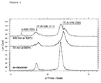
- the as-deposited layer consisted of single-phase [NaCl] structure, see fig. 3.
- the h-AlN (100) peak could not be detected, i.e. the ratio K is equal to zero for all layers.
- the c-(Ti 0.36 Al 0.58 V 0.06 )N (200) peak separated into two peaks of different lattice parameter.
Landscapes
- Chemical & Material Sciences (AREA)
- Chemical Kinetics & Catalysis (AREA)
- Engineering & Computer Science (AREA)
- Materials Engineering (AREA)
- Mechanical Engineering (AREA)
- Metallurgy (AREA)
- Organic Chemistry (AREA)
- Physics & Mathematics (AREA)
- Thermal Sciences (AREA)
- Cutting Tools, Boring Holders, And Turrets (AREA)
- Physical Vapour Deposition (AREA)
- Golf Clubs (AREA)
- Dental Preparations (AREA)
- Paints Or Removers (AREA)
Abstract
- x is between 0.50 and 0.80,
- the ratio, R=x/(x+y), is between 0.50 and 0.85,
- the sum of Ti and Al subscript, S=x+y, is between 0.7 and 1.0
- the ratio of the peak width, F10/90, (FW10%M or FW90%M meaning Full Width at 10% and 90% of the maximum peak value reduced with the background) measured using X-ray diffraction with Cu Kα radiation of the 200 peak at approximately 43 °2 of the (TiyAlxMe1-x-y)N coating is higher than 7.5,
- the ratio between the area of the h-AlN (100) peak at approximately 33 °2 (=A(h-AlN)100) and the c-(TiyAlxMe1-x-y)N (200) peak at approximately 43 °2 (=A(c-(Ti,Al,Me)N)200) called K, i.e. K=A(h-AlN)100/ A(c-(Ti,Al,Me)N)200, and K is between 0 and 0.3 and
- the layer consists of a single (TiyAlxMe1-x-y)N (200) peak.
Description
- The present invention relates to a cutting tool for machining by chip removal consisting of a substrate of cemented carbide, cermet, ceramics, cubic boron nitride based material or high speed steel and a hard and wear resistant refractory coating of which at least one layer comprises a precipitation hardened (TiyAlxMe1-x-y)N based layer, where Me is one of the elements Zr, Hf, V, Nb, Ta, Cr, Mo, W or Si.
- Since the early 1980's, golden-coloured TiN-layers have been widely used for surface protective applications. In order to improve the oxidation resistance of these coatings, work began in the mid-1980's with adding aluminium to TiN [see e.g. H. A. Jehn, et al, J. Vac. Sci. Technol. A 4, 2701 (1986) and O. Knotek et.al, J. Vac. Sci. Technol. A 4, 2695 (1986)]. The compound thus formed, cubic-phase Ti1-xAlxN, was found to have superior oxidation resistance and enabled greater cutting speeds during machining, prolonged tool life, machining of harder materials, and improved manufacturing economy.
- The mechanisms responsible for the excellent cutting performance of Ti1-xAlxN-coated tools have this far been associated with the coating's oxidation resistance. B.-J. Kim et.al., J. Vac. Sci. Technol. A 17(1), 133 (1999) reported that an increased aluminium content in the Ti1-xAlxN compound improves the oxidation resistance. TiN oxidises rapidly at temperatures of 500-600°C according to W.-D. Münz, invited paper Int. Conf. Met. Coat., San Diego, USA (1986) and H. G. Tompkins, J. Appl. Phys. 70, 3876 (1991), whereas oxidation of Ti1-xAlxN starts at 750-900°C, D. McIntyre et. Al., J. Appl. Phys. 67, 1542 (1990).]. This gives an increased upper operating temperature of Ti1-xAlxN compared to TiN from 450-500°C to 750-800°C according to Münz et al., invited paper Int. Conf. Met. Coat., San Diego, USA (1986). This concept of mainly Ti1-xAlxN based materials, has been a subject for a large number of further optimisations of different types, like macroscopically compositional gradients over the coated components as US 5,272,014 discloses. Another way of optimization has been by applying different concepts of multilayer as; alternating Ti and Al containing layers (US 6,309,738), oxygen and non-oxygen containing layers (US 6,254,984), one of the layer stacked in the multilayer consist itself of a multilayer (US 6,077,596), alternating nitrogen content (US 5,330,853) or using one metastable compound (US 5,503,912) or as aperiodic multilayer (US 6,103,357).
- H. Holleck, Surf. Coat. Technol. 36, 151 (1988) reported that the solid solubility of AlN in TiN is extremely low, and only at 2,700 K it reaches ∼5 mol%. For larger AlN fractions, or at lower temperatures, the equilibrium system consists of cubic TiN and hexagonal AlN. However, as is well known Ti1-xAlxN can be deposited as a metastable cubic structure by using physical vapour deposition (PVD). At an elevated temperature during heat treatment or operation of a coated cutting tool, enough energy may then be supplied that phase separation into c-TiN and h-AlN occurs which normally deteriorates the wear resistance of the coating.
- It is an object of the present invention to provide a coating comprising a precipitation hardened (TiyAlxMe1-x-y)N layer applied to a cutting tool for machining by chip removal.
- It is a further object of the present invention to provide a method for depositing crystalline (TiyAlxMe1-x-y)N layers with low compressive residual stresses and hardened by precipitation of nano-crystalline secondary phase(s) using PVD-technique. This type of layer will hereafter be called PREHARD-TiAlN.
- Surprisingly, we have now found that by balancing the chemical composition and the amount of thermal energy added, enhanced performance can be achieved by utilising initial phase separation of the (TiyAlxMe1-x-y)N layer into c-TiN, c-AlN and h-AlN solved in the (TiaAlbMe1-a-b)N matrix in a controlled manner, where a and b are not necessarily the same as x and y. This precipitation hardening effect will then balance the loss in hardness due to the annealing out of structural defects which normally contribute significantly to the hardness of wear resistant PVD-coatings based on nitrides and/or carbides, see e.g. Karlsson et al Thin Solid Films 371 (2000) 36.
-
- Figure 1; X-ray diffraction patterns obtained from (Ti0.34Al0.66) (N0.97O0.03)0.92 layers in as-deposited and annealed conditions.
- Figure 2; Cross-sectional TEM micrographs of (Ti0.34Al0.66) (N0.97O0.03)0.92 layers in (a) as-deposited, (b) 120 min at 900°C (c) 120 min at 1100°C -annealed conditions.
- Figure 3; X-ray diffraction patterns obtained from (Ti0.38Al0.58V0.04)N layers in as-deposited and annealed conditions.
- Figure 4; Schematic drawing showing the definition of the factor F10/90.
-
- According to the present invention there is provided a cutting tool for machining by chip removal comprising a body of a hard alloy of cemented carbide, cermet, ceramics, cubic boron nitride based material or high speed steel onto which a wear resistant coating is deposited composed of one or more layers of refractory compounds comprising at least one PREHARD-TiAlN layer. Additional layer(s) to the PREHARD-TiAlN is composed of metal nitrides and/or carbides and/or oxides with the metal elements chosen from Ti, Zr, Hf, V, Nb, Ta, Cr, Mo, W, Si and Al grown using Physical vapour deposition (PVD) or other deposition technologies than PVD such as plasma enhanced chemical vapour deposition (PACVD) and/or chemical vapour deposition (CVD).
- The PREHARD-TiAlN -layer (s) has a crystalline (TibAlaMe1-a-b)N matrix hardened by precipitation of nano-meter sized cubic TiN (c-TiN), cubic AlN (c-AlN) and hexagonal AlN (h-AlN), crystallites, where a and b are not necessarily the same as x and y describing the overall composition as (TiyAlxMe1-x-y)N. The layer has a low macroscopic compressive residual stress state between 0 and -3.5 GPa, preferably between 0 and -2 GPa. Me is one or several of the elements Zr, Hf, V, Nb, Ta, Cr, Mo, W or Si, preferably V, Zr, Ta and/or Nb, and most preferably Zr and/or Nb. If Me is V and/or Mo it is preferable that the PREHARD-TiAlN is not the outermost layer. If the PREHARD-TiAlN is the outermost layer, and Me is V and/or Mo, those elements should not be present in the very outermost part of the layer, since those metals form low melting point and volatile oxides. This oxidation process will be detrimental for the properties of the PREHARD-TiAlN layer. Therefore the outer 30% of the PREHARD-TiAlN layer is preferably free of V and/or Mo when it is the outermost layer.
- If Me is Ta, the compressive residual stress state of the as-deposited PREHARD-TiAlN layer will increase to very high values due to high momentum ion bombardment during growth of film surface. This high momentum is due to the high average charge state and the high atomic weight of Ta. In order to balance for this, a second Me element should be added, preferably Cr, which due to good surface mobility, heals defects thereby reducing the compressive residual stress. Preferably the content (in atomic%) of Cr (MeCr) is 10-30% higher than the content of Ta (MeTa), i.e. : 1.10 * MeTa < MeCr < 1.30 * MeTa, preferably is 1.10 * MeTa < MeCr < 1.20 * MeTa.
- In (TiyAlxMe1-x-y)N, x is between 0.5 and 0.8, preferably between 0.55 and 0.7. The ratio, R=x/(x+y) is between 0.5 and 0.8 and preferably between 0.55 and 0.7. The sum of the Ti and Al subscripts, S=x+y, is preferably between 0.7 and 1.0, and most preferably between 0.8 and 1.0. In one preferred embodiment x+y=1 and in another x+y<1. The notation here used, (TiyAlxMe1-x-y)N, implies stoichiometry between metal atoms i.e. -between (TiyAlxMe1-x-y) and N. However, perhaps a more accurate notation would be expressed as (TiyAlxMe1-x-y)Nj where j is between 1.2 and 0.8, preferably between 0.9 and 1.05. In further description, the simpler notation of (TiyAlxMe1-x-y)N will be used, except for example 1 where an exact measurement of the stoichiometry has been performed. In addition coatings grown in industrial deposition system always contain a certain amount of oxygen (O) due to residual gases in the system, as demonstrated in example 1, a fact not accounted for in the simpler notation. However, the fact that exact notations in respect of stoichiometry and oxygen content are not used should not restrict the validity of this invention.
- The precipitation hardened (TiyAlxMe1-x-y)N layer has an enhanced hardness, toughness and thermal stability, due to a controlled transformation of the cubic (rocksalt structure) (TiyAlxMe1-x-y)N layer into hexagonal h-AlN, c-TiN and c-AlN in a matrix of (TiaAlbMe1-a-b)N where a and b not necessarily are the same as x and y. The layer is characterised by:
- the ratio of the peak broadening, F10/90, (FW10%M or FW90%M meaning Full Width at 10% and 90% of the maximum peak value which is reduced with the background (see fig. 4)) measured on the 200 peak at approximately 43 °2 (using Cu Kα radiation) of the (TiyAlxMe1-x-y)N coating being >7.5, preferably >9.
- the ratio between the area of the h-AlN (100) peak at approximately 33 °2 (=A(h-AlN)100) and the c-(TiyAlxMe1-x-y)N (200) peak at approximately 43 °2 (=A(c-(Ti,Al,Me)N)200) called K, i.e. K=A(h-AlN)100/ A(c-(Ti,Al,Me)N)200. K is preferably between 0 and 0.3 and most preferably between 0 and 0.2.
- PREHARD-TiAlN layer(s) include one single (TiyAlxMe1-x-y)N (200) peak without several maxima, e.g. as the case of 480 min sample in fig.3. If several maxima occur originating from the same single layer, e.g. two, three or more peaks, this is an indication that a transformation process has proceeded too far. The structure obtained when several peaks occur is too coarse due to large precipitates and should not be considered as the precipitation hardened structure denoted herein as PREHARD-TiAlN according to this invention.
- The PREHARD-TiAlN layer(s) can also be deposited directly onto the cutting tool substrate. The thickness of said PREHARD-TiAlN layer(s) varies then between 0.5 and 12 µm, preferably between 0.5 and 8 µm, especially for machining by chip removal. The total coating thickness, if the PREHARD-TiAlN layer(s) according to the present invention is combined with other layer(s), varies between 0.5 and 15 µm, preferably between 1 and 12 µm with the thickness of the non-PREHARD-TiAlN -layer(s) varying between 0.5 and 8 µm.
- In an alternative embodiment the PREHARD-TiAlN -layer(s) of 0.5 and 10 µm, with or without other layer(s) as described above. An outer 0.5 to 5 µm thick layer consisting of a solid low friction material based on MoS2 or a MeC/C, where Me is Cr, W, Ti or Ta, can be deposited on top of the coating.
- In another alternative embodiment the PREHARD-TiAlN layer(s) between 0.1 and 2 µm are one of 1 to 5 different materials in a 1.0 to 15 µm thick multi-layer coating composed of 2-500, preferably 5-200, individually layers.
- In yet an alternative embodiment the PREHARD-TiAlN -layer(s) of 0.5 and 20 µm can be deposited on top of a CVD coating which may comprise one or several layer(s) of a crystalline Al2O3.
- The method used to grow the coatings comprising a PREHARD-TiAlN - layer(s) of the present invention is based on arc evaporation of an alloy or composite cathode under the following conditions:
- Ti/Al-cathode composition between (50 at% Ti + 50 at% Al) and (20 at% Ti + 80 at% Al), preferably between (40 at% Ti + 60 at% Al) and (30 at% Ti + 70 at% Al).
-
- Evaporation current between 50 A and 200 A depending on cathode size and using cathodes of 63 mm in diameter preferably between 50 A and 80 A.
- Ar/N2 atmosphere consisting of 0-50 vol% Ar, preferably 0-20 vol%, at total pressure of 1.0 Pa to 9.0 Pa, preferably 1.5 Pa to 5.0 Pa.
- Substrate bias of -10 V to -300 V, preferably -40 V to -120.
- Deposition temperature between 400°C and 700°C, preferably 500°C and 650°C.
- To grow a (TiyAlxMe1-x-y)N, where Me is one or several of the elements Zr, Hf, V, Nb, Ta, Cr, Mo, W or Si, alloyed cathodes are used. An alternative is to use one/several pure Me cathode(s) and position this/these cathodes at a longer distance from the substrates than the Ti/Al cathodes are positioned. In this way the preferred alloying of the (Ti,Al)N layer can also be made.
- If pure V or Zr cathode(s) is/are used the evaporation current is preferably between 60 A and 90 A, for Nb and Ta between 80 A and 100. Those current values are suitable for cathodes of 63 mm in diameter but will be different for other sizes.
- Since the (TiyAlxMe1-x-y)N-phase also forms metal carbonitride or carbonitrooxide compounds, and by using PVD-technique to grow the PREHARD-TiAlN-layer, carbon and/or oxygen containing gas can be added to the atmosphere during deposition (e.g. C2H2 or CH4, CO, O2), so that carbon/oxygen alloyed PREHARD-TiAlN can be obtained (e.g. (TiyAlxMe1-x-y)N1-d-eCdOe where d+e is between 0 and 0.2).
- Annealing is preferably performed in inert atmosphere of Ar and/or N2 at a temperature between 800°C and 1100°C over a period of 5 to 240 min. However, the optimal temperature and period is given by the initial phase separation as can be seen by XRD analysis. The annealing can also be performed in-situ in the deposition system, if the system can generate enough thermal energy to obtain the preferred initial phase separation. One possibility to obtain the initial phase separation is to deposit a CVD coating, at a deposition temperature of 800°C to 1050°C, on top of the as-deposited TiAlN layer.
- The present invention has been described with reference to layer(s) of a PREHARD-TiAlN deposited using arc evaporation. PREHARD-TiAlN -layer(s) also could be produced using other PVD-technologies as magnetron sputtering, electron beam evaporation, ion plating or laser ablation.
- Cemented carbide substrates with composition 93.5 wt% WC - 6 wt% Co - 0.5 wt% (Ta,Nb)C were used. The WC grain size was about 1 µm and the hardness was 1630 HV10. The substrates were ground on diamond disks and polished using fine-grained diamond slurry in order to obtain a mirror like surface for the material analysis.
- Before deposition, the substrates were cleaned in ultrasonic baths of an alkali solution and alcohol. The shortest cathode-to-substrate distance was 160 mm. The system was evacuated to a pressure of less than 2.0×10⁻³ Pa, after which the substrates were sputter cleaned with Ar ions. The (Ti,Al)N layer was grown using arc evaporation of six Ti/Al (33 at% Ti + 67 at% Al) cathodes (63 mm in diameter) in an 99.995% pure N2 atmosphere at total pressure of 2.0 Pa, using a substrate bias of -90 V. The deposition was carried out during 60 min in order to obtain a coating thickness of approximately 3 µm. The deposition temperature was ~ 530°C. Immediately after deposition the chamber was vented with dry N2.
- Isothermal post annealing of the coated inserts was carried out at various temperatures in a hot-wall quartz-tube furnace with a 0.40 m long constant temperature (±5°C) zone. The inserts were inserted into the furnace, which was already heated to and stabilised at the desired temperature. The annealing experiments were performed in flowing Ar at atmospheric pressure for a period of 120 min.
- A separate layer,
thickness 300 nm, intended for chemical characterisation was deposited onto a pure C substrate using identical process parameters. The chemical analysis was performed by Rutherford backscattering spectrometry (RBS), using 4He+ ions of 1.8 MeV kinetic energy and a scattering angle of 170°. The RUMP software was used for evaluating raw data. The obtained composition of the as-deposited layer was (Ti0.34Al0.66) (N0.97O0.03)0.92. - The XRD (X-ray diffraction) pattern, using Cu Kα radiation and a configuration with a constant grazing incidence angle of 2° of the as-deposited and annealed (Ti0.34Al0.66) (N0.97O0.03)0.92layers are shown in figure 1. The as-deposited layer consists of a single-phase [NaCl] structure. The (200) peak was positioned at 43.5 °2. For annealing at 600°C the F10/90 value remained constant. For annealing temperatures from 600°C to 900°C the F10/90 value increased from 6 to 10. It can clearly be seen in figure 1 that annealing at 900°C resulted in a broadening of the base of the peak and a sharpening at the top. This is the change in symmetry, which is reflected by an increased F10/90 value. Annealing at 1100°C made the c-(Ti0.34Al0.66) (N0.97O0.03)0.92 (200) peak position shift towards lower 2 values, coming very close to the position for unstrained TiN (200) peak. Peaks originating from h-AlN were also found to appear after annealing at 1100°C. Annealing at 1250°C resulted in a strong peak from Co (111) at 44 °2 as a result of Co migration up onto the coating surface during this high temperature annealing. The F10/90 values of the layers annealed at 1100°C and 1250°C are close to the values of the as-deposited layer.
- The macroscopic residual stress state of the layers was determined by using a substrate curvature technique described by Ramsey et al, Surf. Coat. Technol. 43-44, 223 (1990) and Stoney Proc. R. Soc. London A 82, 172 (1909). The coated WC-Co platelets, 5×5×0.8 mm3, were prepared by cutting, grinding and polishing to a final thickness between 200-300 µm. The macroscopic residual stress of the layers was compressive and largest in the as-deposited at -2.3±0.5 GPa (assuming EWC-6wt%Co=600 GPa, νWC-Co=0.22). Annealing at 900°C for 120 min resulted in stress relaxation to -1.2 GPa, see table 2.
- Cross-sectional transmission electron microscope (TEM) was used to study the microstructure of the coatings. The sample preparation consisted of mechanical grinding and polishing followed by ion-beam sputter etching on both upper and lower surfaces. Cross-sectional TEM micrographs of the as-deposited (Ti0.34Al0.66) (N0.97O0.03)0.92 layers (Fig. 2a) revealed a dense and columnar microstructure with a high defect density and overlapping strain fields due to residual stresses. With respect to the initialised phase separation at 900°C observed by XRD, the micrographs of the annealed sample revealed a structure similar to the as-deposited condition, except for column boundaries appearing more clearly defined. Annealing at 1100°C resulted in phase separation of the metastable c-(Ti,Al)N structure into h-AlN precipitates in a c-(Ti,Al)N matrix, as evidenced by the selected-area electron diffraction (SAED) patterns. Original column boundaries were also dissolved at this temperature, and a fine-textured structure consisting of sub-grains of diameter 50-100 nm evolved. The texture was of a feather-like type with the subgrains spreading out in the growth direction in bundles limited by the parent grain; the parent grain being defined by original column boundaries in the 900°C-annealed condition. From a comparison of SAED patterns in Figs. 2 b) and (c), it appears that each sub-grain has inherited the initial orientation of the respective parent grain, however, within a few degrees of misorientation. Higher-magnification electron micrographs of this structure (inset Fig. 2c) reveal nanometer-sized grains of both cubic and hexagonal structure. After annealing at 1250°C, grains of both hexagonal and cubic phase were found to coarsen and become evenly distributed throughout the entire layer thickness. In addition, the grains adopted an equiaxed geometry with average diameter ∼50 nm.
- Scratch testing resulted in a critical load, FN,C, of the as-deposited layer of ∼60 N. After annealing an enhanced adhesion of variant B to E could be detected with a maximum FN,C of ∼80 N of variant E. For higher annealing temperature FN,C decreased. Very low FN,C was seen for variant G annealed at 1250°C of ∼20 N, se table 2.
VarIant Annealing Temp.[°C] K (h-100)/
(c-200)Shape
c-(200)F10/90 A As-dep. 0 One peak 6.4 B 600 0 One peak 6.3 C 700 0 One peak 7.4 D 800 0 One peak 8.3 E 900 0 One peak 10.0 F 1100 0.22 One peak 6.1 G 1250 0.17 Multiple 6.3 Variant Critical load
FNC [N]Macro Residual stress
σM [GPa]Hardness.
H [GPa]Coating morphology A 60 -2.3±0.5 33.9 Columnar B 60 - 33.8 Columnar C 70 - 35.6 Columnar D 70 - 31.1 Columnar E 80 -1.2±0.1 35.8 Columnar F 50 - 30.6 Nanocrystalline. G 20 - 28.4 Equiaxed - Similar substrates as in example 1 were coated with a single layer of (TiyAlxMe1-x-y)N where Me is V. The substrates were positioned on a fixture of drum type on a position just in front of one Ti/Al cathode (33 at% Ti + 67 at% Al). One V-cathode (99.9 at%) was off set in height from the substrates with 20 cm. The composition of the layer analysed with Energy Dispersiv Spectroscopy (EDS) gave a notation of (Ti0.36Al0.58V0.06)N. The ratio between metal atoms and nitrogen could not be measured using this technique, but it is assumed in the notation to be stoichiometric i.e. one. This composition gives R=x/(x+y)=0.62 and S=x+y=0.94. The coating thickness was 4 µm. The as-deposited samples were isothermally post-annealed at 900°C in an Ar atmosphere at atmospheric pressure for different periods ranging from 0 (=as-deposited) to 480 min. The samples were analysed by XRD using constant gracing incident geometry of 2° 2 using Cu Kα radiation.
- The as-deposited layer consisted of single-phase [NaCl] structure, see fig. 3. After the longest periods of annealing at 900°C, the h-AlN (100) peak could not be detected, i.e. the ratio K is equal to zero for all layers. However, for the longest periods of annealing the c-(Ti0.36Al0.58V0.06)N (200) peak separated into two peaks of different lattice parameter.
- The change of the (Ti0.36Al0.58V0.06)N (200) peak shape was studied expressed as the ratio F10/90. Also in this material system can it be seen that the F10/90 has a maximum after a period of annealing, see table 3.
Variant Period of annealing K (h-100)/
(c-200)Shape
c- (200)F10/90 H As-dep. 0 One peak 7.1 I 10 0 One peak 11.2 J 30 0 One peak 18.2 K 60 0.01 One peak 14.1 L 120 0.02 One peak 6.5 M 240 0.02 One peak 6.8 N 480 0.03 Two peaks 8.7 - Cemented carbide cutting tool inserts with composition 93.5 wt% WC - 6 wt% Co - 0.5 wt% (Ta,Nb)C, were coated and annealed according to example 1 (the same names of the variants are used).
- Face milling tests with homogeneous and interrupted cut were performed in
DIN 42 CrMo 4. The homogeneous test was made in an 60 mm wide plate and the interrupted by using three 20 mm wide plates separated by 10 mm, mounted as a package. The cutting data were; vc = 250 m/min (homogeneous) and 200 m/min (interrupted), f = 0.1 mm/rev and depth of cut = 2.5 mm.Variant Homogeneous cut Interrupted cut F10/90 Tool life, mm Tool life, mm A 3300 2200 6.4 B 2900 2600 6.3 C 3100 2550 7.4 D 2950 3050 8.3 E 2700 3400 10.0 F 2100 2700 6.1 G 950 600 6.3 - This test demonstrates that the variant E has the best toughness without a large drop in tool life in homogeneous cut. Variant E has also the highest F10/90 value.
- Cemented carbide cutting tool inserts with composition 93.5 wt% WC - 6 wt% Co - 0.5 wt% (Ta,Nb)C, were coated and annealed according to example 2 (the same names of the variants are used).
- Face milling tests with interrupted cut were performed in
DIN 42 CrMo 4 according to example 3Variant Interrupted cut F10/90 Tool life, mm H 2050 7.1 I 2400 11.2 J 2900 18.2 K 3100 14.1 L 2700 6.5 M Failure 6.8 N 1650 8.7 - Some of the variants from example 1 were tested in a square shoulder-milling test in stainless steel using following cutting data:
- Insert: SONX 120405TR-M12, WC-10 wt% Co
- Material: DIN X5 CrNi 18 10
- Vc=250 m/min
- fz=0.2 mm
- ap=2.5mm, ae=25 mm
- Cutter diameter 125 mm
-
- This test demonstrates that the variant E has the best toughness. Variant A was worn out due to chippage at the depth of cut.
- A variant grown using same deposition data as variant A but thinner, 1 µm, was annealed for different periods at 900°C and tested in interrupted cut according to example 2.
Variant Annealing Period at 900°C
[min]K (h-100)/
(c-200)Shape
c-(200)F10/90 Interrupted cut
Tool life [mm]O 0 0 One peak 7,19 1100 P 15 0 One peak 10,06 1650 Q 30 0 One peak 12,46 1900 R 60 0 One peak 8,85 1400 S 120 0 One peak 7,23 1500 T 240 0 Two peaks 12,53 1200 U 480 0 Two peaks 10,73 1350 - This test demonstrates the enhanced toughness and tool life follows the F10/90 value as long as only one peak occurs.
| Variant | Tool life, mm | F10/90 |
| A | 2700 | 6.4 |
| E | 3600 | 10.1 |
| F | 1900 | 6.1 |
| | 600 | 6.3 |
Claims (9)
- Cutting tool insert comprising a substrate and a coating characterised in that the coating is composed of one or more layers of refractory compounds of which at least one layer comprises a precipitation hardened (TiyAlxMe1-x-y)N based layer, where Me is one of the elements Zr, Hf, V, Nb, Ta, Cr, Mo, W or Si, defined by:x is between 0.50 and 0.80the ratio, R=x/(x+y), is between 0.50 and 0.85the sum of Ti and Al subscripts, S=x+y, is between 0.7 and 1.0the ratio of the peak width, F10/90, (FW10%M or FW90%M meaning Full Width at 10% and 90% of the maximum peak value reduced with the background) measured using X-ray diffraction with Cu Kα radiation of the 200 peak at approximately 43 °2 of the (TiyAlXMe1-x-y)N coating is higher than 7.5the ratio between the area of the h-AlN (100) peak at approximately 33 °2 (=A(h-AlN)100) and the c-(TiyAlxMe1-x-y)N (200) peak at approximately 43 °2 (=A(c-(Ti,Al,Me)N)200) called K, i.e. K=A(h-AlN)100/ A(c-(Ti,Al,Me)N)200, and K is between 0 and 0.3the layer consists of a single (TiyAlxMe1-x-y)N (200) peak.
- Cutting tool insert according to claim 1 characterised in that:x is between 0.55 and 0.70the ratio, R=x/(x+y), is between 0.55 and 0.75the sum of Ti and Al subscript, S=x+y, is between 0.8 and 1.0the F10/90 is higher than 8.
- Cutting tool according to claim 2 characterised in that:x is between 0.60 and 0.70the ratio, R=x/(x+y), is between 0.60 and 0.75the F10/90 is higher than 9K is between 0 and 0.2
- Cutting tool according to any of the preceding claims characterised in that x+y=1.
- Cutting tool according to any of claims 1-3 characterised in that x+y<1.
- Cutting tool according to claim 5 characterised in that Me= V, Zr, Ta, Nb, Si or Cr.
- Cutting tool according to claim 6 characterised in that Me= Zr or Nb.
- Cutting tool according to any of the preceding claims characterised in that said layer is deposited with PVD technique and the precipitates are obtained by a spinodal decomposition of the cubic (TiyAlxMe1-x-y)N layer.
- Cutting tool according to any of the preceding claims characterised in that the precipitates consist of nano-meter sized cubic TiN (c-TiN) and cubic AlN (c-AlN) and/or hexagonal AlN (h-AlN).
Applications Claiming Priority (2)
| Application Number | Priority Date | Filing Date | Title |
|---|---|---|---|
| SE0202631 | 2002-09-04 | ||
| SE0202631A SE526338C2 (en) | 2002-09-04 | 2002-09-04 | Cut with a hardened, hardened refractory coating |
Publications (2)
| Publication Number | Publication Date |
|---|---|
| EP1400609A1 true EP1400609A1 (en) | 2004-03-24 |
| EP1400609B1 EP1400609B1 (en) | 2006-11-29 |
Family
ID=20288906
Family Applications (1)
| Application Number | Title | Priority Date | Filing Date |
|---|---|---|---|
| EP03019946A Expired - Lifetime EP1400609B1 (en) | 2002-09-04 | 2003-09-02 | Precipitation hardened wear resistant coating |
Country Status (5)
| Country | Link |
|---|---|
| US (1) | US7056602B2 (en) |
| EP (1) | EP1400609B1 (en) |
| AT (1) | ATE346965T1 (en) |
| DE (1) | DE60309992T2 (en) |
| SE (1) | SE526338C2 (en) |
Cited By (31)
| Publication number | Priority date | Publication date | Assignee | Title |
|---|---|---|---|---|
| EP1722009A1 (en) * | 2005-05-06 | 2006-11-15 | Seco Tools Ab | Thin wear resistant coating |
| EP1798310A3 (en) * | 2005-12-14 | 2007-10-03 | Sandvik Intellectual Property AB | Cemented carbide inserts for wear demanding parting and grooving in heat resistant super alloys (HRSA) and stainless steels |
| EP1798308A3 (en) * | 2005-12-14 | 2007-10-03 | Sandvik Intellectual Property AB | Cemented carbide inserts for notch and wear demanding turning in heat resistant super alloys (HRSA) and stainless steels |
| WO2009011650A1 (en) * | 2007-07-13 | 2009-01-22 | Seco Tools Ab | Fine grained cemented carbide for turning in heat resistant super alloys (hrsa) |
| DE102012017731A1 (en) | 2012-09-08 | 2014-03-13 | Oerlikon Trading Ag, Trübbach | Ti-Al-Ta based coating with improved temperature resistance |
| RU2532741C1 (en) * | 2013-07-12 | 2014-11-10 | Федеральное государственное бюджетное образовательное учреждение высшего профессионального образования "Ульяновский государственный технический университет" | Method of obtaining multi-layered coating for cutting instrument |
| RU2538060C1 (en) * | 2013-07-23 | 2015-01-10 | Федеральное государственное бюджетное образовательное учреждение высшего профессионального образования "Ульяновский государственный технический университет" | Method for obtaining multi-layered coating for cutting tool |
| RU2538055C1 (en) * | 2013-07-23 | 2015-01-10 | Федеральное государственное бюджетное образовательное учреждение высшего профессионального образования "Ульяновский государственный технический университет" | Method for obtaining multi-layered coating for cutting tool |
| RU2538056C1 (en) * | 2013-07-23 | 2015-01-10 | Федеральное государственное бюджетное образовательное учреждение высшего профессионального образования "Ульяновский государственный технический университет" | Method for obtaining multi-layered coating for cutting tool |
| RU2538057C1 (en) * | 2013-07-12 | 2015-01-10 | Федеральное государственное бюджетное образовательное учреждение высшего профессионального образования "Ульяновский государственный технический университет" | Method for obtaining multi-layered coating for cutting tool |
| RU2545885C2 (en) * | 2013-07-23 | 2015-04-10 | Федеральное государственное бюджетное образовательное учреждение высшего профессионального образования "Ульяновский государственный технический университет" | Method of obtaining multi-layered coating for cutting instrument |
| RU2561578C1 (en) * | 2014-10-28 | 2015-08-27 | Федеральное государственное бюджетное образовательное учреждение высшего профессионального образования "Ульяновский государственный технический университет" | Method of producing sandwiched coating for cutting tool |
| RU2566217C1 (en) * | 2014-10-28 | 2015-10-20 | Федеральное государственное бюджетное образовательное учреждение высшего профессионального образования "Ульяновский государственный технический университет" | Method of producing sandwiched coating for cutting tool |
| RU2566222C1 (en) * | 2014-10-28 | 2015-10-20 | Федеральное государственное бюджетное образовательное учреждение высшего профессионального образования "Ульяновский государственный технический университет" | Method of producing sandwiched coating for cutting tool |
| RU2566221C1 (en) * | 2014-10-28 | 2015-10-20 | Федеральное государственное бюджетное образовательное учреждение высшего профессионального образования "Ульяновский государственный технический университет" | Method of producing sandwiched coating for cutting tool |
| RU2566216C1 (en) * | 2014-10-28 | 2015-10-20 | Федеральное государственное бюджетное образовательное учреждение высшего профессионального образования "Ульяновский государственный технический университет" | Method of producing sandwiched coating for cutting tool |
| CN105026083A (en) * | 2013-03-04 | 2015-11-04 | 株式会社图格莱 | Coated cutting tool |
| CN106103793A (en) * | 2015-01-14 | 2016-11-09 | 住友电工硬质合金株式会社 | The manufacture method of hard coat, cutting element and hard coat |
| RU2616718C1 (en) * | 2015-10-27 | 2017-04-18 | Федеральное государственное бюджетное образовательное учреждение высшего профессионального образования "Ульяновский государственный технический университет" | Method of producing sandwiched coating for cutting tool |
| RU2620528C2 (en) * | 2015-10-27 | 2017-05-26 | федеральное государственное бюджетное образовательное учреждение высшего образования "Ульяновский государственный технический университет" | Method of producing sandwiched coating for cutting tool |
| RU2620532C2 (en) * | 2015-11-10 | 2017-05-26 | федеральное государственное бюджетное образовательное учреждение высшего образования "Ульяновский государственный технический университет" | Method of producing sandwiched coating for cutting tool |
| RU2620529C1 (en) * | 2015-12-15 | 2017-05-26 | федеральное государственное бюджетное образовательное учреждение высшего образования "Ульяновский государственный технический университет" | Method of producing sandwiched coating for cutting tool |
| RU2622528C1 (en) * | 2015-12-15 | 2017-06-16 | федеральное государственное бюджетное образовательное учреждение высшего образования "Ульяновский государственный технический университет" | Method of producing sandwiched coating for cutting tool |
| RU2622527C1 (en) * | 2015-12-15 | 2017-06-16 | федеральное государственное бюджетное образовательное учреждение высшего образования "Ульяновский государственный технический университет" | Method of producing sandwiched coating for cutting tool |
| RU2630734C1 (en) * | 2016-10-11 | 2017-09-12 | федеральное государственное бюджетное образовательное учреждение высшего образования "Ульяновский государственный технический университет" | Method of producing sandwiched coating for cutting tool |
| RU2637863C1 (en) * | 2016-10-11 | 2017-12-07 | федеральное государственное бюджетное образовательное учреждение высшего образования "Ульяновский государственный технический университет" | Method of producing multi-layer coating for cutting tool |
| RU2637862C1 (en) * | 2016-10-11 | 2017-12-07 | федеральное государственное бюджетное образовательное учреждение высшего образования "Ульяновский государственный технический университет" | Method of producing multi-layer coating for cutting tool |
| RU2640690C1 (en) * | 2016-10-11 | 2018-01-11 | федеральное государственное бюджетное образовательное учреждение высшего образования "Ульяновский государственный технический университет" | Method of producing multi-layer coating for cutting tool |
| DE102006000259B4 (en) * | 2005-05-31 | 2018-02-22 | Osg Corp. | Multi-layer hard material layer and use in a coated with the multi-layer hard layer tool |
| WO2018215558A1 (en) | 2017-05-23 | 2018-11-29 | Oerlikon Surface Solutions Ag, Pfäffikon | Thick TiAlTaN/AlCrN multilayer coating films on turbine components |
| RU2784931C1 (en) * | 2022-06-30 | 2022-12-01 | федеральное государственное бюджетное образовательное учреждение высшего образования "Казанский национальный исследовательский технический университет им. А.Н.Туполева-КАИ" | Method for applying a protective coating to a metal mold for casting aluminum alloys |
Families Citing this family (48)
| Publication number | Priority date | Publication date | Assignee | Title |
|---|---|---|---|---|
| DE102006004394B4 (en) * | 2005-02-16 | 2011-01-13 | Kabushiki Kaisha Kobe Seiko Sho (Kobe Steel, Ltd.), Kobe-shi | Hard film, multilayer hard film and manufacturing method therefor |
| SE529161C2 (en) * | 2005-06-22 | 2007-05-22 | Seco Tools Ab | Cutting tool with composite coating for fine machining of hardened steels |
| JP5188133B2 (en) * | 2006-09-27 | 2013-04-24 | 京セラ株式会社 | Cutting tools |
| SE0602814L (en) * | 2006-12-27 | 2008-06-28 | Sandvik Intellectual Property | Cutting tool with multilayer coating |
| AT9999U1 (en) * | 2007-06-29 | 2008-07-15 | Ceratizit Austria Gmbh | AL-TI-RU-N-C HARD COAT LAYER |
| JP4774080B2 (en) * | 2007-08-02 | 2011-09-14 | 株式会社神戸製鋼所 | Hard coating material and cold plastic working mold |
| US7947363B2 (en) * | 2007-12-14 | 2011-05-24 | Kennametal Inc. | Coated article with nanolayered coating scheme |
| EP2247772B1 (en) * | 2008-02-21 | 2016-06-29 | Seco Tools AB | Multilayered coated cutting tool |
| EP2098611B1 (en) | 2008-03-07 | 2013-02-13 | Seco Tools AB | Layered coated cutting tool |
| KR100876366B1 (en) * | 2008-04-24 | 2008-12-31 | 한국야금 주식회사 | Multi-layer Hard Thin Films for Cutting Tools |
| SE533884C2 (en) | 2009-06-01 | 2011-02-22 | Seco Tools Ab | Nanolaminated coated cutting tool |
| SE533883C2 (en) | 2009-06-01 | 2011-02-22 | Seco Tools Ab | Nanolaminated coated cutting tool |
| WO2011016488A1 (en) * | 2009-08-04 | 2011-02-10 | 株式会社タンガロイ | Coated member |
| WO2011122553A1 (en) * | 2010-03-29 | 2011-10-06 | 京セラ株式会社 | Cutting tool |
| US8586214B2 (en) * | 2010-03-29 | 2013-11-19 | Kyocera Corporation | Cutting tool |
| EP2578339B1 (en) * | 2010-05-27 | 2015-07-29 | Kyocera Corporation | Cutting tool |
| US8945251B2 (en) * | 2010-09-29 | 2015-02-03 | Kyocera Corporation | Cutting tool |
| US8440328B2 (en) * | 2011-03-18 | 2013-05-14 | Kennametal Inc. | Coating for improved wear resistance |
| WO2013045454A2 (en) * | 2011-09-30 | 2013-04-04 | Cemecon Ag | Coating of substrates using hipims |
| RU2491367C1 (en) * | 2012-02-29 | 2013-08-27 | Федеральное государственное бюджетное образовательное учреждение высшего профессионального образования "Московский государственный технологический университет "СТАНКИН" (ФГБОУ ВПО МГТУ "СТАНКИН") | Method of making cutting ceramic plates from nitride ceramics |
| EP2636764B1 (en) | 2012-03-07 | 2014-07-09 | Seco Tools Ab | Nanolaminated coated cutting tool |
| AR092945A1 (en) * | 2012-10-10 | 2015-05-06 | Oerlikon Trading Ag Trübbach | COATING FOR HIGH TEMPERATURE USES WITH TRIBOLOGICAL REQUEST |
| JP6206133B2 (en) * | 2012-11-30 | 2017-10-04 | 三菱マテリアル株式会社 | Surface coated cutting tool |
| US9103036B2 (en) | 2013-03-15 | 2015-08-11 | Kennametal Inc. | Hard coatings comprising cubic phase forming compositions |
| WO2014157688A1 (en) * | 2013-03-28 | 2014-10-02 | 日立ツール株式会社 | Coated cutting tool and method for producing same |
| RU2545955C2 (en) * | 2013-07-23 | 2015-04-10 | Федеральное государственное бюджетное образовательное учреждение высшего профессионального образования "Ульяновский государственный технический университет" | Method of producing sandwiched coating for cutting tool |
| JP6092735B2 (en) * | 2013-07-31 | 2017-03-08 | 京セラ株式会社 | Surface coating tool |
| US9896767B2 (en) | 2013-08-16 | 2018-02-20 | Kennametal Inc | Low stress hard coatings and applications thereof |
| US9168664B2 (en) | 2013-08-16 | 2015-10-27 | Kennametal Inc. | Low stress hard coatings and applications thereof |
| JP6206800B2 (en) * | 2013-09-05 | 2017-10-04 | 住友電工ハードメタル株式会社 | Method for producing coating film |
| KR101551963B1 (en) * | 2013-09-12 | 2015-09-10 | 현대자동차주식회사 | Coating material for aluminum die casting and method for coating the same |
| JP6491031B2 (en) * | 2014-06-24 | 2019-03-27 | 株式会社神戸製鋼所 | Laminated hard coating and cutting tool |
| JP6555796B2 (en) * | 2014-09-26 | 2019-08-07 | 日立金属株式会社 | Coated cutting tool |
| JP2016199793A (en) * | 2015-04-13 | 2016-12-01 | 株式会社神戸製鋼所 | Hard film |
| JP6519795B2 (en) * | 2015-09-30 | 2019-05-29 | 三菱マテリアル株式会社 | Surface coated cutting tool with excellent chipping resistance and wear resistance |
| RU2622526C2 (en) * | 2015-10-27 | 2017-06-16 | федеральное государственное бюджетное образовательное учреждение высшего образования "Ульяновский государственный технический университет" | Method of producing sandwiched coating for cutting tool |
| RU2620527C2 (en) * | 2015-10-27 | 2017-05-26 | федеральное государственное бюджетное образовательное учреждение высшего образования "Ульяновский государственный технический университет" | Method of producing sandwiched coating for cutting tool |
| RU2622533C1 (en) * | 2015-12-15 | 2017-06-16 | федеральное государственное бюджетное образовательное учреждение высшего образования "Ульяновский государственный технический университет" | Method of producing sandwiched coating for cutting tool |
| RU2622539C1 (en) * | 2015-12-15 | 2017-06-16 | федеральное государственное бюджетное образовательное учреждение высшего образования "Ульяновский государственный технический университет" | Method of producing multi-layer coating for cutting tool |
| RU2622538C1 (en) * | 2015-12-15 | 2017-06-16 | федеральное государственное бюджетное образовательное учреждение высшего образования "Ульяновский государственный технический университет" | Method of producing multi-layer coating for cutting tool |
| US9994958B2 (en) | 2016-01-20 | 2018-06-12 | Sumitomo Electric Hardmetal Corp. | Coating, cutting tool, and method of manufacturing coating |
| DE202018006896U1 (en) | 2017-02-13 | 2024-03-12 | Oerlikon Surface Solutions Ag, Pfäffikon | High-temperature stable, compositionally modulated hard material coatings |
| KR102821766B1 (en) * | 2018-10-26 | 2025-06-16 | 외를리콘 서피스 솔루션즈 아게, 페피콘 | Vanadium aluminum nitride (VAlN) microalloyed with Ti and/or Si |
| WO2020084166A1 (en) * | 2018-10-26 | 2020-04-30 | Oerlikon Surface Solutions Ag, Pfäffikon | Pvd coatings with a hea ceramic matrix with controlled precipitate structure |
| JP7707063B2 (en) * | 2018-11-09 | 2025-07-14 | エリコン・サーフェス・ソリューションズ・アクチェンゲゼルシャフト,プフェフィコーン | Al-rich cubic AlTiN coatings deposited from ceramic targets |
| DE102021106674A1 (en) * | 2021-03-18 | 2022-09-22 | Fraunhofer-Gesellschaft zur Förderung der angewandten Forschung eingetragener Verein | AlN-based hard material layer on bodies made of metal, hard metal, cermet or ceramic and method for their production |
| WO2023191078A1 (en) * | 2022-03-31 | 2023-10-05 | 京セラ株式会社 | Coated tool and cutting tool |
| CN116288214B (en) * | 2023-03-30 | 2024-07-12 | 兰州理工大学 | High-entropy ceramic gradient coating with high interface bonding strength and preparation method and application thereof |
Citations (4)
| Publication number | Priority date | Publication date | Assignee | Title |
|---|---|---|---|---|
| EP0592986A1 (en) * | 1992-10-12 | 1994-04-20 | Sumitomo Electric Industries, Limited | Ultra-thin film laminate |
| US5330853A (en) * | 1991-03-16 | 1994-07-19 | Leybold Ag | Multilayer Ti-Al-N coating for tools |
| EP0947607A2 (en) * | 1998-03-16 | 1999-10-06 | Hitachi Tool Engineering, Ltd. | Members with multi-layer coatings |
| US20020028323A1 (en) * | 2000-12-22 | 2002-03-07 | Mitsubishi Materials Corporation | Coated cutting tool |
Family Cites Families (12)
| Publication number | Priority date | Publication date | Assignee | Title |
|---|---|---|---|---|
| DE3825399C5 (en) * | 1988-07-23 | 2005-05-12 | Cemecon Ag | PVD or plasma CVD coating |
| JP2793772B2 (en) * | 1994-05-13 | 1998-09-03 | 神鋼コベルコツール株式会社 | Hard film coated tools and hard film coated members with excellent adhesion |
| JP3229947B2 (en) | 1996-04-26 | 2001-11-19 | 日立ツール株式会社 | Surface-coated indexable inserts |
| DE69730576T2 (en) * | 1996-12-04 | 2005-02-03 | Sumitomo Electric Industries, Ltd. | Coated tool and method for its manufacture |
| SE518145C2 (en) * | 1997-04-18 | 2002-09-03 | Sandvik Ab | Multilayer coated cutting tool |
| JP4185172B2 (en) * | 1997-06-19 | 2008-11-26 | 住友電工ハードメタル株式会社 | Coated hard tool |
| JPH11131216A (en) * | 1997-10-29 | 1999-05-18 | Hitachi Tool Eng Ltd | Coated hard tool |
| EP0972091A1 (en) * | 1998-02-04 | 2000-01-19 | OSG Corporation | Multilayer coated tool |
| JP3454148B2 (en) | 1998-04-27 | 2003-10-06 | 三菱マテリアル株式会社 | Surface coated cemented carbide cutting tool with excellent wear resistance with hard coating layer |
| JP3599628B2 (en) * | 2000-02-25 | 2004-12-08 | 株式会社タンガロイ | Composite hard film coated member |
| US6811581B2 (en) * | 2000-10-31 | 2004-11-02 | Mitsubishi Materials Kobe Tools Corporation | High-speed tool steel gear cutting tool and manufacturing method therefor |
| EP1219723B1 (en) * | 2000-12-28 | 2006-10-25 | Kabushiki Kaisha Kobe Seiko Sho | Hard film for cutting tools |
-
2002
- 2002-09-04 SE SE0202631A patent/SE526338C2/en not_active IP Right Cessation
-
2003
- 2003-09-02 DE DE60309992T patent/DE60309992T2/en not_active Expired - Lifetime
- 2003-09-02 AT AT03019946T patent/ATE346965T1/en active
- 2003-09-02 EP EP03019946A patent/EP1400609B1/en not_active Expired - Lifetime
- 2003-09-03 US US10/653,244 patent/US7056602B2/en not_active Expired - Fee Related
Patent Citations (4)
| Publication number | Priority date | Publication date | Assignee | Title |
|---|---|---|---|---|
| US5330853A (en) * | 1991-03-16 | 1994-07-19 | Leybold Ag | Multilayer Ti-Al-N coating for tools |
| EP0592986A1 (en) * | 1992-10-12 | 1994-04-20 | Sumitomo Electric Industries, Limited | Ultra-thin film laminate |
| EP0947607A2 (en) * | 1998-03-16 | 1999-10-06 | Hitachi Tool Engineering, Ltd. | Members with multi-layer coatings |
| US20020028323A1 (en) * | 2000-12-22 | 2002-03-07 | Mitsubishi Materials Corporation | Coated cutting tool |
Non-Patent Citations (1)
| Title |
|---|
| S. MENZEL ET AL.: "Phase transition in PACVD-(Ti,Al)N coatings after annealing", SURFACE AND COATINGS TECHNOLOGY, vol. 124, 2000, pages 190 - 195, XP002266241 * |
Cited By (36)
| Publication number | Priority date | Publication date | Assignee | Title |
|---|---|---|---|---|
| EP1722009A1 (en) * | 2005-05-06 | 2006-11-15 | Seco Tools Ab | Thin wear resistant coating |
| DE102006000259B4 (en) * | 2005-05-31 | 2018-02-22 | Osg Corp. | Multi-layer hard material layer and use in a coated with the multi-layer hard layer tool |
| EP1798310A3 (en) * | 2005-12-14 | 2007-10-03 | Sandvik Intellectual Property AB | Cemented carbide inserts for wear demanding parting and grooving in heat resistant super alloys (HRSA) and stainless steels |
| EP1798308A3 (en) * | 2005-12-14 | 2007-10-03 | Sandvik Intellectual Property AB | Cemented carbide inserts for notch and wear demanding turning in heat resistant super alloys (HRSA) and stainless steels |
| WO2009011650A1 (en) * | 2007-07-13 | 2009-01-22 | Seco Tools Ab | Fine grained cemented carbide for turning in heat resistant super alloys (hrsa) |
| US7989092B2 (en) | 2007-07-13 | 2011-08-02 | Seco Tools Ab | Fine grained cemented carbide for turning in heat resistant super alloys (HRSA) |
| US8187430B2 (en) | 2007-07-13 | 2012-05-29 | Seco Tools Ab | Method of making a coated cemented carbide insert |
| DE102012017731A1 (en) | 2012-09-08 | 2014-03-13 | Oerlikon Trading Ag, Trübbach | Ti-Al-Ta based coating with improved temperature resistance |
| WO2014037104A1 (en) | 2012-09-08 | 2014-03-13 | Oerlikon Trading Ag, Trübbach | Ti-al-ta-based coating exhibiting enhanced thermal stability |
| CN105026083A (en) * | 2013-03-04 | 2015-11-04 | 株式会社图格莱 | Coated cutting tool |
| CN105026083B (en) * | 2013-03-04 | 2017-02-08 | 株式会社图格莱 | Coated cutting tool |
| RU2532741C1 (en) * | 2013-07-12 | 2014-11-10 | Федеральное государственное бюджетное образовательное учреждение высшего профессионального образования "Ульяновский государственный технический университет" | Method of obtaining multi-layered coating for cutting instrument |
| RU2538057C1 (en) * | 2013-07-12 | 2015-01-10 | Федеральное государственное бюджетное образовательное учреждение высшего профессионального образования "Ульяновский государственный технический университет" | Method for obtaining multi-layered coating for cutting tool |
| RU2545885C2 (en) * | 2013-07-23 | 2015-04-10 | Федеральное государственное бюджетное образовательное учреждение высшего профессионального образования "Ульяновский государственный технический университет" | Method of obtaining multi-layered coating for cutting instrument |
| RU2538056C1 (en) * | 2013-07-23 | 2015-01-10 | Федеральное государственное бюджетное образовательное учреждение высшего профессионального образования "Ульяновский государственный технический университет" | Method for obtaining multi-layered coating for cutting tool |
| RU2538055C1 (en) * | 2013-07-23 | 2015-01-10 | Федеральное государственное бюджетное образовательное учреждение высшего профессионального образования "Ульяновский государственный технический университет" | Method for obtaining multi-layered coating for cutting tool |
| RU2538060C1 (en) * | 2013-07-23 | 2015-01-10 | Федеральное государственное бюджетное образовательное учреждение высшего профессионального образования "Ульяновский государственный технический университет" | Method for obtaining multi-layered coating for cutting tool |
| RU2566216C1 (en) * | 2014-10-28 | 2015-10-20 | Федеральное государственное бюджетное образовательное учреждение высшего профессионального образования "Ульяновский государственный технический университет" | Method of producing sandwiched coating for cutting tool |
| RU2561578C1 (en) * | 2014-10-28 | 2015-08-27 | Федеральное государственное бюджетное образовательное учреждение высшего профессионального образования "Ульяновский государственный технический университет" | Method of producing sandwiched coating for cutting tool |
| RU2566222C1 (en) * | 2014-10-28 | 2015-10-20 | Федеральное государственное бюджетное образовательное учреждение высшего профессионального образования "Ульяновский государственный технический университет" | Method of producing sandwiched coating for cutting tool |
| RU2566217C1 (en) * | 2014-10-28 | 2015-10-20 | Федеральное государственное бюджетное образовательное учреждение высшего профессионального образования "Ульяновский государственный технический университет" | Method of producing sandwiched coating for cutting tool |
| RU2566221C1 (en) * | 2014-10-28 | 2015-10-20 | Федеральное государственное бюджетное образовательное учреждение высшего профессионального образования "Ульяновский государственный технический университет" | Method of producing sandwiched coating for cutting tool |
| CN106103793A (en) * | 2015-01-14 | 2016-11-09 | 住友电工硬质合金株式会社 | The manufacture method of hard coat, cutting element and hard coat |
| CN106103793B (en) * | 2015-01-14 | 2019-06-07 | 住友电工硬质合金株式会社 | The manufacturing method of hard coat, cutting element and hard coat |
| RU2616718C1 (en) * | 2015-10-27 | 2017-04-18 | Федеральное государственное бюджетное образовательное учреждение высшего профессионального образования "Ульяновский государственный технический университет" | Method of producing sandwiched coating for cutting tool |
| RU2620528C2 (en) * | 2015-10-27 | 2017-05-26 | федеральное государственное бюджетное образовательное учреждение высшего образования "Ульяновский государственный технический университет" | Method of producing sandwiched coating for cutting tool |
| RU2620532C2 (en) * | 2015-11-10 | 2017-05-26 | федеральное государственное бюджетное образовательное учреждение высшего образования "Ульяновский государственный технический университет" | Method of producing sandwiched coating for cutting tool |
| RU2622528C1 (en) * | 2015-12-15 | 2017-06-16 | федеральное государственное бюджетное образовательное учреждение высшего образования "Ульяновский государственный технический университет" | Method of producing sandwiched coating for cutting tool |
| RU2622527C1 (en) * | 2015-12-15 | 2017-06-16 | федеральное государственное бюджетное образовательное учреждение высшего образования "Ульяновский государственный технический университет" | Method of producing sandwiched coating for cutting tool |
| RU2620529C1 (en) * | 2015-12-15 | 2017-05-26 | федеральное государственное бюджетное образовательное учреждение высшего образования "Ульяновский государственный технический университет" | Method of producing sandwiched coating for cutting tool |
| RU2630734C1 (en) * | 2016-10-11 | 2017-09-12 | федеральное государственное бюджетное образовательное учреждение высшего образования "Ульяновский государственный технический университет" | Method of producing sandwiched coating for cutting tool |
| RU2637863C1 (en) * | 2016-10-11 | 2017-12-07 | федеральное государственное бюджетное образовательное учреждение высшего образования "Ульяновский государственный технический университет" | Method of producing multi-layer coating for cutting tool |
| RU2637862C1 (en) * | 2016-10-11 | 2017-12-07 | федеральное государственное бюджетное образовательное учреждение высшего образования "Ульяновский государственный технический университет" | Method of producing multi-layer coating for cutting tool |
| RU2640690C1 (en) * | 2016-10-11 | 2018-01-11 | федеральное государственное бюджетное образовательное учреждение высшего образования "Ульяновский государственный технический университет" | Method of producing multi-layer coating for cutting tool |
| WO2018215558A1 (en) | 2017-05-23 | 2018-11-29 | Oerlikon Surface Solutions Ag, Pfäffikon | Thick TiAlTaN/AlCrN multilayer coating films on turbine components |
| RU2784931C1 (en) * | 2022-06-30 | 2022-12-01 | федеральное государственное бюджетное образовательное учреждение высшего образования "Казанский национальный исследовательский технический университет им. А.Н.Туполева-КАИ" | Method for applying a protective coating to a metal mold for casting aluminum alloys |
Also Published As
| Publication number | Publication date |
|---|---|
| SE526338C2 (en) | 2005-08-23 |
| US7056602B2 (en) | 2006-06-06 |
| US20040110039A1 (en) | 2004-06-10 |
| DE60309992D1 (en) | 2007-01-11 |
| EP1400609B1 (en) | 2006-11-29 |
| DE60309992T2 (en) | 2007-09-20 |
| SE0202631L (en) | 2004-03-05 |
| ATE346965T1 (en) | 2006-12-15 |
| SE0202631D0 (en) | 2002-09-04 |
Similar Documents
| Publication | Publication Date | Title |
|---|---|---|
| EP1400609B1 (en) | Precipitation hardened wear resistant coating | |
| US7083868B2 (en) | Composite structured wear resistant coating | |
| CN100525968C (en) | Thin wear resistant coating | |
| KR101831014B1 (en) | Coated cutting tool insert | |
| US9540722B2 (en) | Body with a metal based nitride layer and a method for coating the body | |
| JP6858347B2 (en) | Cover cutting tool | |
| US6673430B2 (en) | PVD Al2O3 coated cutting tool | |
| EP0592986B1 (en) | Ultra-thin film laminate | |
| EP1877595B1 (en) | Cutting tool insert, solid end mill or drill coated with wear resistant layer. | |
| RU2507303C2 (en) | NON GAMMA-PHASE CUBIC AlCrO | |
| US7838132B2 (en) | PVD-coated cutting tool insert | |
| US12319996B2 (en) | Cutting tool | |
| KR20100126356A (en) | Oxide Coated Cutting Inserts | |
| EP3929328B1 (en) | Coated cutting tool | |
| JP7288602B2 (en) | coated cutting tools | |
| JPH08281502A (en) | Crystal orientating coated tool | |
| JP7741303B2 (en) | Coated and cutting tools | |
| JP7750272B2 (en) | Coated Cutting Tools | |
| EP4624622A1 (en) | Cutting tool with tialn-layer | |
| JP2023014653A (en) | Coated cutting tool | |
| WO2022239139A1 (en) | Cutting tool |
Legal Events
| Date | Code | Title | Description |
|---|---|---|---|
| PUAI | Public reference made under article 153(3) epc to a published international application that has entered the european phase |
Free format text: ORIGINAL CODE: 0009012 |
|
| AK | Designated contracting states |
Kind code of ref document: A1 Designated state(s): AT BE BG CH CY CZ DE DK EE ES FI FR GB GR HU IE IT LI LU MC NL PT RO SE SI SK TR |
|
| AX | Request for extension of the european patent |
Extension state: AL LT LV MK |
|
| 17P | Request for examination filed |
Effective date: 20040907 |
|
| AKX | Designation fees paid |
Designated state(s): AT BE BG CH CY CZ DE DK EE ES FI FR GB GR HU IE IT LI LU MC NL PT RO SE SI SK TR |
|
| 17Q | First examination report despatched |
Effective date: 20041202 |
|
| GRAP | Despatch of communication of intention to grant a patent |
Free format text: ORIGINAL CODE: EPIDOSNIGR1 |
|
| GRAS | Grant fee paid |
Free format text: ORIGINAL CODE: EPIDOSNIGR3 |
|
| GRAA | (expected) grant |
Free format text: ORIGINAL CODE: 0009210 |
|
| AK | Designated contracting states |
Kind code of ref document: B1 Designated state(s): AT BE BG CH CY CZ DE DK EE ES FI FR GB GR HU IE IT LI LU MC NL PT RO SE SI SK TR |
|
| PG25 | Lapsed in a contracting state [announced via postgrant information from national office to epo] |
Ref country code: BE Free format text: LAPSE BECAUSE OF FAILURE TO SUBMIT A TRANSLATION OF THE DESCRIPTION OR TO PAY THE FEE WITHIN THE PRESCRIBED TIME-LIMIT Effective date: 20061129 Ref country code: FI Free format text: LAPSE BECAUSE OF FAILURE TO SUBMIT A TRANSLATION OF THE DESCRIPTION OR TO PAY THE FEE WITHIN THE PRESCRIBED TIME-LIMIT Effective date: 20061129 Ref country code: CZ Free format text: LAPSE BECAUSE OF FAILURE TO SUBMIT A TRANSLATION OF THE DESCRIPTION OR TO PAY THE FEE WITHIN THE PRESCRIBED TIME-LIMIT Effective date: 20061129 Ref country code: SI Free format text: LAPSE BECAUSE OF FAILURE TO SUBMIT A TRANSLATION OF THE DESCRIPTION OR TO PAY THE FEE WITHIN THE PRESCRIBED TIME-LIMIT Effective date: 20061129 Ref country code: NL Free format text: LAPSE BECAUSE OF FAILURE TO SUBMIT A TRANSLATION OF THE DESCRIPTION OR TO PAY THE FEE WITHIN THE PRESCRIBED TIME-LIMIT Effective date: 20061129 Ref country code: SK Free format text: LAPSE BECAUSE OF FAILURE TO SUBMIT A TRANSLATION OF THE DESCRIPTION OR TO PAY THE FEE WITHIN THE PRESCRIBED TIME-LIMIT Effective date: 20061129 Ref country code: RO Free format text: LAPSE BECAUSE OF FAILURE TO SUBMIT A TRANSLATION OF THE DESCRIPTION OR TO PAY THE FEE WITHIN THE PRESCRIBED TIME-LIMIT Effective date: 20061129 |
|
| REG | Reference to a national code |
Ref country code: GB Ref legal event code: FG4D |
|
| REG | Reference to a national code |
Ref country code: CH Ref legal event code: EP |
|
| REG | Reference to a national code |
Ref country code: IE Ref legal event code: FG4D |
|
| REF | Corresponds to: |
Ref document number: 60309992 Country of ref document: DE Date of ref document: 20070111 Kind code of ref document: P |
|
| REG | Reference to a national code |
Ref country code: SE Ref legal event code: TRGR |
|
| PG25 | Lapsed in a contracting state [announced via postgrant information from national office to epo] |
Ref country code: BG Free format text: LAPSE BECAUSE OF FAILURE TO SUBMIT A TRANSLATION OF THE DESCRIPTION OR TO PAY THE FEE WITHIN THE PRESCRIBED TIME-LIMIT Effective date: 20070228 Ref country code: DK Free format text: LAPSE BECAUSE OF FAILURE TO SUBMIT A TRANSLATION OF THE DESCRIPTION OR TO PAY THE FEE WITHIN THE PRESCRIBED TIME-LIMIT Effective date: 20070228 |
|
| PG25 | Lapsed in a contracting state [announced via postgrant information from national office to epo] |
Ref country code: ES Free format text: LAPSE BECAUSE OF FAILURE TO SUBMIT A TRANSLATION OF THE DESCRIPTION OR TO PAY THE FEE WITHIN THE PRESCRIBED TIME-LIMIT Effective date: 20070312 |
|
| REG | Reference to a national code |
Ref country code: CH Ref legal event code: NV Representative=s name: BOVARD AG PATENTANWAELTE |
|
| PG25 | Lapsed in a contracting state [announced via postgrant information from national office to epo] |
Ref country code: PT Free format text: LAPSE BECAUSE OF FAILURE TO SUBMIT A TRANSLATION OF THE DESCRIPTION OR TO PAY THE FEE WITHIN THE PRESCRIBED TIME-LIMIT Effective date: 20070430 |
|
| NLV1 | Nl: lapsed or annulled due to failure to fulfill the requirements of art. 29p and 29m of the patents act | ||
| ET | Fr: translation filed | ||
| PLBE | No opposition filed within time limit |
Free format text: ORIGINAL CODE: 0009261 |
|
| STAA | Information on the status of an ep patent application or granted ep patent |
Free format text: STATUS: NO OPPOSITION FILED WITHIN TIME LIMIT |
|
| 26N | No opposition filed |
Effective date: 20070830 |
|
| PG25 | Lapsed in a contracting state [announced via postgrant information from national office to epo] |
Ref country code: MC Free format text: LAPSE BECAUSE OF NON-PAYMENT OF DUE FEES Effective date: 20070930 Ref country code: GR Free format text: LAPSE BECAUSE OF FAILURE TO SUBMIT A TRANSLATION OF THE DESCRIPTION OR TO PAY THE FEE WITHIN THE PRESCRIBED TIME-LIMIT Effective date: 20070301 |
|
| PG25 | Lapsed in a contracting state [announced via postgrant information from national office to epo] |
Ref country code: IE Free format text: LAPSE BECAUSE OF NON-PAYMENT OF DUE FEES Effective date: 20070903 |
|
| PG25 | Lapsed in a contracting state [announced via postgrant information from national office to epo] |
Ref country code: EE Free format text: LAPSE BECAUSE OF FAILURE TO SUBMIT A TRANSLATION OF THE DESCRIPTION OR TO PAY THE FEE WITHIN THE PRESCRIBED TIME-LIMIT Effective date: 20061129 |
|
| PG25 | Lapsed in a contracting state [announced via postgrant information from national office to epo] |
Ref country code: CY Free format text: LAPSE BECAUSE OF FAILURE TO SUBMIT A TRANSLATION OF THE DESCRIPTION OR TO PAY THE FEE WITHIN THE PRESCRIBED TIME-LIMIT Effective date: 20061129 Ref country code: LU Free format text: LAPSE BECAUSE OF NON-PAYMENT OF DUE FEES Effective date: 20070902 |
|
| PG25 | Lapsed in a contracting state [announced via postgrant information from national office to epo] |
Ref country code: TR Free format text: LAPSE BECAUSE OF FAILURE TO SUBMIT A TRANSLATION OF THE DESCRIPTION OR TO PAY THE FEE WITHIN THE PRESCRIBED TIME-LIMIT Effective date: 20061129 Ref country code: HU Free format text: LAPSE BECAUSE OF FAILURE TO SUBMIT A TRANSLATION OF THE DESCRIPTION OR TO PAY THE FEE WITHIN THE PRESCRIBED TIME-LIMIT Effective date: 20070530 |
|
| REG | Reference to a national code |
Ref country code: CH Ref legal event code: PFA Owner name: SECO TOOLS AB Free format text: SECO TOOLS AB# #S-737 82 FAGERSTA (SE) -TRANSFER TO- SECO TOOLS AB# #S-737 82 FAGERSTA (SE) |
|
| PGFP | Annual fee paid to national office [announced via postgrant information from national office to epo] |
Ref country code: CH Payment date: 20110913 Year of fee payment: 9 |
|
| PGFP | Annual fee paid to national office [announced via postgrant information from national office to epo] |
Ref country code: SE Payment date: 20120911 Year of fee payment: 10 Ref country code: GB Payment date: 20120829 Year of fee payment: 10 |
|
| PGFP | Annual fee paid to national office [announced via postgrant information from national office to epo] |
Ref country code: IT Payment date: 20120915 Year of fee payment: 10 Ref country code: DE Payment date: 20120829 Year of fee payment: 10 Ref country code: FR Payment date: 20120926 Year of fee payment: 10 |
|
| PGFP | Annual fee paid to national office [announced via postgrant information from national office to epo] |
Ref country code: AT Payment date: 20120829 Year of fee payment: 10 |
|
| REG | Reference to a national code |
Ref country code: SE Ref legal event code: EUG |
|
| PG25 | Lapsed in a contracting state [announced via postgrant information from national office to epo] |
Ref country code: SE Free format text: LAPSE BECAUSE OF NON-PAYMENT OF DUE FEES Effective date: 20130903 |
|
| REG | Reference to a national code |
Ref country code: CH Ref legal event code: PL |
|
| REG | Reference to a national code |
Ref country code: AT Ref legal event code: MM01 Ref document number: 346965 Country of ref document: AT Kind code of ref document: T Effective date: 20130902 |
|
| GBPC | Gb: european patent ceased through non-payment of renewal fee |
Effective date: 20130902 |
|
| REG | Reference to a national code |
Ref country code: DE Ref legal event code: R119 Ref document number: 60309992 Country of ref document: DE Effective date: 20140401 |
|
| REG | Reference to a national code |
Ref country code: FR Ref legal event code: ST Effective date: 20140530 |
|
| PG25 | Lapsed in a contracting state [announced via postgrant information from national office to epo] |
Ref country code: CH Free format text: LAPSE BECAUSE OF NON-PAYMENT OF DUE FEES Effective date: 20130930 Ref country code: GB Free format text: LAPSE BECAUSE OF NON-PAYMENT OF DUE FEES Effective date: 20130902 Ref country code: LI Free format text: LAPSE BECAUSE OF NON-PAYMENT OF DUE FEES Effective date: 20130930 |
|
| PG25 | Lapsed in a contracting state [announced via postgrant information from national office to epo] |
Ref country code: IT Free format text: LAPSE BECAUSE OF NON-PAYMENT OF DUE FEES Effective date: 20130902 Ref country code: FR Free format text: LAPSE BECAUSE OF NON-PAYMENT OF DUE FEES Effective date: 20130930 Ref country code: AT Free format text: LAPSE BECAUSE OF NON-PAYMENT OF DUE FEES Effective date: 20130902 Ref country code: DE Free format text: LAPSE BECAUSE OF NON-PAYMENT OF DUE FEES Effective date: 20140401 |