EP1720122B1 - Method for manufacturing a portable data carrier - Google Patents
Method for manufacturing a portable data carrier Download PDFInfo
- Publication number
- EP1720122B1 EP1720122B1 EP06007847A EP06007847A EP1720122B1 EP 1720122 B1 EP1720122 B1 EP 1720122B1 EP 06007847 A EP06007847 A EP 06007847A EP 06007847 A EP06007847 A EP 06007847A EP 1720122 B1 EP1720122 B1 EP 1720122B1
- Authority
- EP
- European Patent Office
- Prior art keywords
- electronic circuit
- data carrier
- portable data
- recess
- tool
- Prior art date
- Legal status (The legal status is an assumption and is not a legal conclusion. Google has not performed a legal analysis and makes no representation as to the accuracy of the status listed.)
- Not-in-force
Links
Images

Classifications
-
- G—PHYSICS
- G06—COMPUTING; CALCULATING OR COUNTING
- G06K—GRAPHICAL DATA READING; PRESENTATION OF DATA; RECORD CARRIERS; HANDLING RECORD CARRIERS
- G06K19/00—Record carriers for use with machines and with at least a part designed to carry digital markings
- G06K19/06—Record carriers for use with machines and with at least a part designed to carry digital markings characterised by the kind of the digital marking, e.g. shape, nature, code
- G06K19/067—Record carriers with conductive marks, printed circuits or semiconductor circuit elements, e.g. credit or identity cards also with resonating or responding marks without active components
- G06K19/07—Record carriers with conductive marks, printed circuits or semiconductor circuit elements, e.g. credit or identity cards also with resonating or responding marks without active components with integrated circuit chips
- G06K19/077—Constructional details, e.g. mounting of circuits in the carrier
-
- G—PHYSICS
- G06—COMPUTING; CALCULATING OR COUNTING
- G06K—GRAPHICAL DATA READING; PRESENTATION OF DATA; RECORD CARRIERS; HANDLING RECORD CARRIERS
- G06K19/00—Record carriers for use with machines and with at least a part designed to carry digital markings
- G06K19/06—Record carriers for use with machines and with at least a part designed to carry digital markings characterised by the kind of the digital marking, e.g. shape, nature, code
- G06K19/067—Record carriers with conductive marks, printed circuits or semiconductor circuit elements, e.g. credit or identity cards also with resonating or responding marks without active components
- G06K19/07—Record carriers with conductive marks, printed circuits or semiconductor circuit elements, e.g. credit or identity cards also with resonating or responding marks without active components with integrated circuit chips
- G06K19/073—Special arrangements for circuits, e.g. for protecting identification code in memory
- G06K19/07309—Means for preventing undesired reading or writing from or onto record carriers
- G06K19/07345—Means for preventing undesired reading or writing from or onto record carriers by activating or deactivating at least a part of the circuit on the record carrier, e.g. ON/OFF switches
Definitions
- the invention relates to a method for producing a portable data carrier. Furthermore, the invention relates to a semifinished product for producing a portable data carrier and a portable data carrier.
- a portable data carrier As part of the manufacturing process for a portable data carrier is a common practice is to completely or partially surround an electronic circuit with a material, in particular with a plastic material.
- the electronic circuit is usually an integrated circuit, in particular a microcontroller.
- the electronic circuit can be inserted into a card body, wherein subsequently further manufacturing steps are carried out.
- plastic materials as part of the manufacturing process may lead to electrostatic charges, by which the electronic circuit of the portable data carrier is placed in an undefined state.
- the portable data carrier When the electronic circuit is in an undefined state, the portable data carrier is unusable. Nevertheless, in order to be able to use the portable data carrier, it is necessary to restore the electronic circuit from the undefined state to a defined state.
- reset and resets the electronic circuit In order to enable a transfer from an undefined to a defined state, in particular designed as microcontroller electronic circuits often have a function which is referred to as reset and resets the electronic circuit, starting from an arbitrary state to a ground state. This reset is usually caused by applying a designated signal to the electronic circuit.
- DE 10101330 A1 shows a circuit arrangement for protecting the circuit from mechanical manipulation. In response to a detected mechanical manipulation of a circuit over the protective layer, the function of the circuit is disabled. A similar manipulation protection shows DE 102 51317 A1 , The claims are against this document.
- Electronic circuits with reset function are also used in portable data carriers, especially in smart cards.
- a reset signal is applied from the outside to a designated contact surface of the smart card.
- only electronic circuits can be reset by smart cards, which have a contact surface for contacting contact in this way.
- a data carrier with a first interface for a first communication signal and a second interface for a second communication signal is known. From the communication signals in each case a clock signal is derived and tested by means of one frequency sensor. A processor is reset if the first communication signal falls below a first clock frequency or the second communication signal falls below a second clock frequency.
- the US 5 068 521 B1 discloses a contactless smart card having a battery and whose CPU is reset via a reset line. After resetting the CPU, the chip card is formed overall as a potting body, so that the reset line is no longer accessible. The CPU remains in operation after the reset until the battery is exhausted. Furthermore, the disclosure US 5 068 521 B1 a contactless chip card, which has a device for detecting a reset signal. When a reset signal is detected, this device causes the CPU to be initialized. The reset signal is transmitted without contact by means of an electromagnetic wave. The detection of the reset signal via the frequency or the amplitude of the electromagnetic wave.
- the known approaches are limited to embodiments of the portable data carrier in which the electronic circuit is accessible from the outside.
- the invention has for its object to prevent as reliable as possible that an electronic circuit of a portable data carrier is permanently placed in an undefined state in the manufacture of the portable data carrier and thereby the portable data carrier is unusable.
- At least one electronic circuit is connected to an electrically conductive structure with the aid of which a transfer of the electronic circuit into a defined state can be triggered.
- the electronic circuit and the electrically conductive structure are surrounded by a material such that the electrically conductive structure is no longer accessible for a contacting contact.
- the surrounding material is partially removed with the help of a tool and the Conversion of the electronic circuit triggered in the defined state.
- the invention has the advantage that the yield in the production of portable data carriers can be increased with relatively little effort. Should the electronic circuit of a portable data carrier be brought into an undefined state during the manufacturing process, for example by electrostatic charging, a reliable return of the electronic circuit to a defined state is achieved with the method according to the invention. In this way, it can be prevented that the portable data carrier becomes permanently unusable as a result of the undefined state of the electronic circuit.
- the method according to the invention is designed in such a way that, when the material is removed, an electrical contact is temporarily formed between the tool and the electrically conductive structure. About this contact, a signal can be transmitted, which triggers the transfer of the electronic circuit in a defined state. Furthermore, it can be provided that, when removing the material, a plurality of elements of the electrically conductive structure are connected to one another in an electrically conductive manner.
- the transfer of the electronic circuit is triggered in the defined state in the formation of a recess.
- the recess is formed in particular by means of a tool.
- the dimensions of the tool should optionally be chosen so that it can be electrically conductively connected to each other, the plurality of elements of the electrically conductive structure.
- the dimensions of the tool can be selected so that the minimum distance between terminal contacts, which are arranged in the region of the recess, is not bridged in the formation of the recess by the tool. This ensures that no unwanted short circuit between the terminals is triggered by the tool.
- a component of the portable data carrier in particular a further electronic circuit can be used.
- the electrically conductive structure after completion of the portable data carrier is no longer accessible and unwanted transfer of the electronic circuit can not be done in a defined state in the use of the portable data carrier.
- the recess it is also possible to form the recess as a through hole.
- the through hole can be formed at the very end of the manufacturing process, so that in this variant the transfer the electronic circuit in the defined state can be done at a very late date.
- the transfer of the electronic circuit is triggered in the defined state in the formation of the outer contour of the portable data carrier.
- a material-removing intervention in the portable data carrier itself is not required.
- the invention further relates to a semi-finished product for producing at least one portable data carrier.
- the semifinished product according to the invention has at least one electronic circuit which is connected to an electrically conductive structure. By a contacting contacting of the electrically conductive structure, a transfer of the electronic circuit in a defined state can be triggered.
- the peculiarity of the semi-finished product according to the invention is that the electrically conductive structure is surrounded by a material such that it is not accessible for a contacting contact.
- the electrically conductive structure is preferably designed such that it has a plurality of elements arranged adjacent to one another.
- the electrically conductive structure extends beyond the outer contour provided for the portable data carrier. This allows a transfer of the electronic circuit in a defined state when separating the portable data carrier from the semifinished product.
- the electrically conductive structure is arranged in a region which is provided for the formation of a recess. This embodiment is for a transfer of the electronic circuit provided in a defined state in the production of the recess.
- the portable data carrier is designed in each case as a chip card.
- the invention is not limited to smart cards, but equally applies to other portable data carriers.
- a portable data carrier in the sense of the invention is to be regarded as a computer system in which the resources, i. Memory resources and / or computing capacity (computing power) are limited, e.g. a chip card (smart card, microprocessor chip card) or a token or a chip module for installation in a chip card or in a token.
- the portable data carrier has a body in which a CPU (microprocessor) is located, and which may have any standardized or non-standardized shape, for example, the shape of a flat chip card with no standard or a standard such as e.g. ISO 7810 (e.g., ID-1, ID-00, ID-000) or a voluminous token.
- the portable data carrier may further have one or more arbitrary interfaces for contactless and / or contact communication with a reader or data processing system (e.g., personal computer, workstation, server).
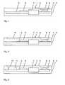
- Fig. 1, 2 and 3 show snapshots at different times during a first variant of the inventive method for producing a chip card 1 each in a schematic sectional view.
- the representation is not strictly limited to a sectional plane, but also shows staggered components of the chip card 1. It was therefore dispensed with the use of hatching. For the sake of clarity, the representation is executed in each case strongly unwholesomestäsch.
- the chip card 1 has a card body 2, which may be designed with respect to its dimensions according to the ISO / IEC 7810 standard and in the illustrated embodiment is composed of a lower half shell 3 and an upper half shell 4.
- the half shells 3 and 4 are preferably made of plastic.
- a flexible printed circuit board 5 with a first microcontroller 6, a battery 7, a button 8 and a display device 9 is arranged between the half-shells 3 and 4, a flexible printed circuit board 5 with a first microcontroller 6, a battery 7, a button 8 and a display device 9 is arranged.
- the first microcontroller 6 is used to control the display device 9.
- the supply voltage for operating the first microcontroller 6 and the display device 9 is provided by the battery 7. With the help of the button 8, the display device 9 can be activated.
- the flexible printed circuit board 5 it is also possible to use a plastic film on which printed conductors are applied, for example by printing with silver conductive paste.
- the first microcontroller 6 is already active and the manufacturing process is in an end stage. Before the in Fig. 1 a multiplicity of method steps have been carried out and there is thus the risk that the first microcontroller 6 has been brought into an undefined state by electrostatic charging effects. If the first microcontroller 6 is actually in an undefined state, the chip card 1 can only be supplied to its intended use if it is possible to reset the first microcontroller 6 to a defined state. However, the first microcontroller 6 is completely embedded in the card body 2 and thus no longer accessible from the outside. The following will be explains how a reset of the first microcontroller 6 in the context of the inventive method is still possible.
- Fig. 2 shows, in the method according to the invention in the upper half-shell 4 of the card body 2, a first recess 10 is milled.
- the first recess 10 is formed in a region of the card body 2, in which, apart from the printed circuit board 5, no further component of the chip card 1 is arranged.
- a second recess 11 is milled into the upper half-shell 4 of the card body 2, which has a smaller lateral extent than the first recess 10 and extends at least to the circuit board 5. This is in Fig. 3 shown.
- the formed in this area on the circuit board 5 structures are in Fig. 4 shown.
- Fig. 4 shows the chip card 1 in the same state as in Fig. 3 in a schematic plan. In this case, such components are indicated, which are located inside the chip card 1.
- connection contacts 12 are arranged on the circuit board. Between two opposite connection contacts 12, an electrode structure 13 is formed.
- the electrode structure 13 has two comb-like interdigitated electrodes 14, which are connected to one of the terminal contacts 12 and extend into the vicinity of the respectively opposite terminal contact 12, but these do not touch.
- the connection of the two terminal contacts 12 connected to the electrodes 14 is in Fig. 4 not shown and can for example be such that one terminal 12 is connected to ground and the other terminal 12 to a reset input of the first microcontroller 6. In this case, the reset input of the first microcontroller 6 can be at the supply voltage level via a pull-up resistor.
- the connection contacts 12 and the electrode structure 13 need not lie in one plane, but may for example lie on two different sides of the circuit board 5.
- a milling tool 15 is shown symbolically, with which the first recess 10 and the second recess 11 are made.
- the milling tool 15 is made of an electrically conductive material.
- connection contacts 12 and in particular also the electrode structure 13 on the circuit board 5 are exposed. During this exposure, it happens once or even several times that the milling tool 15 temporarily connects the two electrodes 14 of the electrode structure 13 to one another.
- the reset input of the first microcontroller 6 is briefly grounded and then pulled back up to supply voltage level by the pull-up resistor.
- Such a change in potential at the reset input of the first microcontroller 6 triggers a reset of the first microcontroller 6, so that the first microcontroller 6 is in a defined state after the shorting of the two electrodes 14 by the milling tool 15.
- the resetting of the first microcontroller 6 is performed properly even if the electrodes 14 are damaged by the milling tool 15 or even destroyed.
- the cross section of the milling tool 15 is chosen so small that the distance between the terminal contacts 12 by the milling tool 15 can not be bridged.
- the cross section of the milling tool 15 is limited by the fact that it must be possible to connect the two electrodes 14 of the electrode structure 13 to one another with the milling tool 15. The further procedure after the formation of the second recess 11 is based on Fig. 5 explained.
- Fig. 5 shows the chip card 1 produced according to the first variant of the method according to the invention in the finished state in a Fig. 1 to 3 corresponding representation.
- a two-stage chip module 16 is inserted into the two recesses 10 and 11 and connected via electrical connection elements 17 to the connection contacts 12 on the circuit board 5.
- the chip module 16 is glued to the card body 2.
- the chip module 16 has a second microcontroller 18 in which, for example, an application software of the chip card 1 is implemented.
- the second microcontroller 18 has access to the display device 9 via the first microcontroller 6.
- the chip module 16 has a contact field 19 for a contacting contact by an external device.
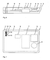
- Fig. 6 shows a chip card 1 produced according to a second variant of the method according to the invention in the finished state in a Fig. 5 corresponding representation.
- An associated schematic plan view is in Fig. 7 shown.
- the resetting of the first microcontroller 6 in the second variant of the method takes place in the formation of a through hole 20 in the card body 2.
- the through hole 20 is preferably formed in the vicinity of a corner of the card body 2 and can serve decoration purposes or even a band, a chain, etc. Record attachment purposes.
- the electrode structure 13 is arranged on the printed circuit board 5 in the region of the through-hole 20 and is severed during the production of the through-hole 20.
- the electrode structure 13 is completely, ie, also drawn within the through-hole 20.
- the electrode structure 13 is no longer present there.
- the through-hole 20 is made, for example, by punching or milling by means of an electrically conductive tool.
- the electrodes 14 of the electrode structure 13 are briefly connected to one another, at least during the severing, so that a reset of the first microcontroller 6 is initiated.
- the first microcontroller 6 is preferably designed such that it is not only capable of controlling the display device 9 but also of assuming tasks of the second microcontroller 18 not provided there.
- Fig. 8 shows a chip card 1 produced according to a third variant of the method according to the invention in the finished state in one Fig. 5 corresponding representation.
- Fig. 9 shows the chip card 1 from Fig. 8 at an earlier time, when it is still part of a bow 21, in one schematic supervision.
- the sheet 21 has the same thickness as the chip card 1 larger lateral dimensions.
- the sheet 21 may have a plurality of laterally juxtaposed chip cards 1.
- Fig. 9 only the outer contour of a single chip card 1 is shown. Instead of the sheet 21 may also be provided a web.
- the circuit board 5 has an extension 22 which extends beyond the outer contour of the chip card 1 addition.
- the electrode structure 13 is arranged, the two electrodes 14 this time not comb-like mesh, but are formed as two mutually parallel conductor tracks.
- the electrodes 14 of the electrode structure 13 are severed.
- the electrodes 14 are briefly connected to each other upon impact of the punching tool, so that a reset of the first microcontroller 6 is triggered.
- neither the production of recesses 10 and 11 nor the production of a through-hole 20 is required for resetting the first microcontroller 6.
Abstract
Description
Die Erfindung betrifft ein Verfahren zur Herstellung eines tragbaren Datenträgers. Weiterhin betrifft die Erfindung ein Halbzeug zur Herstellung eines tragbaren Datenträgers und einen tragbaren Datenträger.The invention relates to a method for producing a portable data carrier. Furthermore, the invention relates to a semifinished product for producing a portable data carrier and a portable data carrier.
Im Rahmen des Herstellungsprozesses für einen tragbaren Datenträger besteht eine übliche Vorgehensweise darin, eine elektronische Schaltung ganz oder teilweise mit einem Material, insbesondere mit einem Kunststoffmaterial zu umgeben. Bei der elektronischen Schaltung handelt es sich in der Regel um einen integrierten Schaltkreis, insbesondere um einen Mikrocontroller. Beispielsweise kann zur Herstellung eines tragbaren Datenträgers, der als eine Chipkarte ausgebildet ist, die elektronische Schaltung in einen Kartenkörper eingesetzt werden, wobei anschließend noch weitere Herstellungsschritte ausgeführt werden. Insbesondere bei der Verwendung von Kunststoffmaterialien kann es im Rahmen des Herstellungsprozesses zu elektrostatischen Aufladungen kommen, durch die die elektronische Schaltung des tragbaren Datenträgers in einen undefinierten Zustand versetzt wird. Wenn sich die elektronische Schaltungin einem undefinierten Zustand befindet, ist der tragbare Datenträger nicht nutzbar. Um den tragbaren Datenträger dennoch einer Nutzung zuführen zu können, ist es erforderlich, die elektronische Schaltung vom undefinierten Zustand wieder in einen definierten Zustand zu überführen.As part of the manufacturing process for a portable data carrier is a common practice is to completely or partially surround an electronic circuit with a material, in particular with a plastic material. The electronic circuit is usually an integrated circuit, in particular a microcontroller. For example, to produce a portable data carrier, which is designed as a chip card, the electronic circuit can be inserted into a card body, wherein subsequently further manufacturing steps are carried out. In particular, when using plastic materials, as part of the manufacturing process may lead to electrostatic charges, by which the electronic circuit of the portable data carrier is placed in an undefined state. When the electronic circuit is in an undefined state, the portable data carrier is unusable. Nevertheless, in order to be able to use the portable data carrier, it is necessary to restore the electronic circuit from the undefined state to a defined state.
Um eine Überführung von einem undefinierten in einen definierten Zustand zu ermöglichen, verfügen insbesondere als Mikrocontroller ausgebildete elektronischen Schaltungen häufig über eine Funktion, die als Reset bezeichnet wird und die elektronische Schaltung ausgehend von einem beliebigen Zustand in einen Grundzustand zurücksetzt. Dieses Zurücksetzen wird in der Regel durch Anlegen eines dafür vorgesehenen Signals an die elektronische Schaltung veranlasst.In order to enable a transfer from an undefined to a defined state, in particular designed as microcontroller electronic circuits often have a function which is referred to as reset and resets the electronic circuit, starting from an arbitrary state to a ground state. This reset is usually caused by applying a designated signal to the electronic circuit.
Gemäß
Elektronische Schaltungen mit Reset-Funktion werden auch bei tragbaren Datenträgern, insbesondere bei Chipkarten, eingesetzt. Beispielsweise wird bei kontaktbehafteten Chipkarten während der Anschaltsequenz gemäß der Norm ISO/IEC 7816-3 ein Reset-Signal von außen an eine dafür vorgesehene Kontaktfläche der Chipkarte angelegt. Allerdings können auf diese Weise nur elektronische Schaltungen von Chipkarten zurückgesetzt werden, die über eine Kontaktfläche zur berührenden Kontaktierung verfügen.Electronic circuits with reset function are also used in portable data carriers, especially in smart cards. For example, in the case of contact smart cards during the power-up sequence according to the standard ISO / IEC 7816-3, a reset signal is applied from the outside to a designated contact surface of the smart card. However, only electronic circuits can be reset by smart cards, which have a contact surface for contacting contact in this way.
Aus der
Die
Die bekannten Vorgehensweisen sind jedoch auf Ausgestaltungen des tragbaren Datenträgers beschränkt, bei denen die elektronische Schaltung von außen zugänglich ist. Es besteht allerdings auch die Möglichkeit, dass eine solche Zugänglichkeit nicht vorgesehen ist. Dies kann beispielsweise dann der Fall sein, wenn für den Betrieb der elektronischen Schaltung eine Zugänglichkeit von außen nicht erforderlich ist. Wenn die elektronische Schaltung bei der Herstellung des tragbaren Datenträgers zu einem Zeitpunkt in einen undefinierten Zustand versetzt wird, zu dem die elektronische Schaltung von außen nicht mehr zugänglich ist, wird der tragbare Datenträger unbrauchbar.However, the known approaches are limited to embodiments of the portable data carrier in which the electronic circuit is accessible from the outside. However, there is also the possibility that such accessibility is not provided. This can be the case, for example, if accessibility from the outside is not required for the operation of the electronic circuit. If the electronic circuit is put into an undefined state during the manufacture of the portable data carrier at a time when the electronic circuit is no longer accessible from the outside, the portable data carrier becomes unusable.
Der Erfindung liegt die Aufgabe zugrunde, möglichst zuverlässig zu verhindern, dass eine elektronische Schaltung eines tragbaren Datenträgers bei der Herstellung des tragbaren Datenträgers dauerhaft in einen undefinierten Zustand versetzt wird und dadurch der tragbare Datenträger unbrauchbar wird.The invention has for its object to prevent as reliable as possible that an electronic circuit of a portable data carrier is permanently placed in an undefined state in the manufacture of the portable data carrier and thereby the portable data carrier is unusable.
Diese Aufgabe wird durch ein Herstellungsverfahren mit der Merkmalskombination des Anspruchs 1 gelöst.This object is achieved by a manufacturing method with the feature combination of
Beim erfindungsgemäßen Verfahren zur Herstellung eines tragbaren Datenträgers wird wenigstens eine elektronische Schaltung mit einer elektrisch leitenden Struktur verbunden, mit deren Hilfe eine Überführung der elektronischen Schaltung in einen definierten Zustand ausgelöst werden kann. Die elektronische Schaltung und die elektrisch leitende Struktur werden derart von einem Material umgeben, dass die elektrisch leitende Struktur für eine berührende Kontaktierung nicht mehr zugänglich ist. Das umgebende Material wird mit Hilfe eines Werkzeugs teilweise entfernt und dabei das Überführen der elektronischen Schaltung in den definierten Zustand ausgelöst.In the method according to the invention for producing a portable data carrier, at least one electronic circuit is connected to an electrically conductive structure with the aid of which a transfer of the electronic circuit into a defined state can be triggered. The electronic circuit and the electrically conductive structure are surrounded by a material such that the electrically conductive structure is no longer accessible for a contacting contact. The surrounding material is partially removed with the help of a tool and the Conversion of the electronic circuit triggered in the defined state.
Die Erfindung hat den Vorteil, dass mit relativ geringem Aufwand die Ausbeute bei der Herstellung von tragbaren Datenträgern erhöht werden kann. Sollte die elektronische Schaltung eines tragbaren Datenträgers im Rahmen des Herstellungsprozesses beispielsweise durch elektrostatische Aufladung in einen undefinierten Zustand gebracht werden, so wird mit dem erfindungsgemäßen Verfahren eine zuverlässige Rückführung der elektronischen Schaltung in einen definierten Zustand erreicht. Auf diese Weise kann verhindert werden, dass der tragbare Datenträger infolge des undefinierten Zustands der elektronischen Schaltung dauerhaft unbrauchbar wird.The invention has the advantage that the yield in the production of portable data carriers can be increased with relatively little effort. Should the electronic circuit of a portable data carrier be brought into an undefined state during the manufacturing process, for example by electrostatic charging, a reliable return of the electronic circuit to a defined state is achieved with the method according to the invention. In this way, it can be prevented that the portable data carrier becomes permanently unusable as a result of the undefined state of the electronic circuit.
Besonders vorteilhaft ist es, wenn das Überführen der elektronischen Schaltung in den definierten Zustand mit demselben Werkzeug ausgelöst wird, mit dem das Material entfernt wird. Dadurch ist es möglich, für das erfindungsgemäße Verfahren herkömmliche Fertigungseinrichtungen einzusetzen, die nicht oder nur geringfügig abgewandelt sind. Außerdem wird ein hoher Durchsatz erreicht, da kein eigener Verfahrensschritt für das Auslösen des Überführens in den undefinierten Zustand erforderlich ist.It when the transfer of the electronic circuit is triggered in the defined state with the same tool with which the material is removed is particularly advantageous. This makes it possible to use conventional manufacturing facilities for the inventive method, which are not or only slightly modified. In addition, a high throughput is achieved, since no separate process step for triggering the transfer to the undefined state is required.
Das erfindungsgemäße Verfahren ist insbesondere so ausgelegt, dass beim Entfernen des Materials zeitweise ein elektrischer Kontakt zwischen dem Werkzeug und der elektrisch leitenden Struktur ausgebildet wird. Über diesen Kontakt kann ein Signal übertragen werden, welches das Überführen der elektronischen Schaltung in einen definierten Zustand auslöst. Weiterhin kann vorgesehen werden, dass beim Entfernen des Materials mehrere Elemente der elektrisch leitenden Struktur miteinander elektrisch leitend verbunden werden.In particular, the method according to the invention is designed in such a way that, when the material is removed, an electrical contact is temporarily formed between the tool and the electrically conductive structure. About this contact, a signal can be transmitted, which triggers the transfer of the electronic circuit in a defined state. Furthermore, it can be provided that, when removing the material, a plurality of elements of the electrically conductive structure are connected to one another in an electrically conductive manner.
Im Rahmen des erfindungsgemäßen Verfahrens kann vorgesehen sein, dass beim Entfernen des Materials die elektrisch leitende Struktur teilweise entfernt wird. Dies vereinfacht das erfindungsgemäße Verfahren erheblich, da keine Maßnahmen zum Schutz der elektrisch leitenden Struktur erforderlich sind. Außerdem werden dadurch Verfahrensvarianten ermöglicht, bei denen es zwangsweise zu einer Entfernung von Teilen der elektrisch leitenden Struktur kommt.In the context of the method according to the invention, provision can be made for the electrically conductive structure to be partially removed when the material is removed. This considerably simplifies the method according to the invention since no measures for protecting the electrically conductive structure are required. In addition, this method variants are made possible, in which it comes forcibly to a removal of parts of the electrically conductive structure.
Gemäß einer Ausgestaltung des erfindungsgemäßen Verfahrens wird das Überführen der elektronischen Schaltung in den definierten Zustand bei der Ausbildung einer Ausnehmung ausgelöst. Die Ausnehmung wird insbesondere mit Hilfe eines Werkzeugs ausgebildet. Die Abmessungen des Werkzeugs sollen gegebenenfalls so gewählt sein, daß es die mehreren Elemente der elektrisch leitenden Struktur miteinander elektrisch leitend verbunden kann. Zudem können die Abmessungen des Werkzeugs so gewählt sein, dass der minimale Abstand zwischen Anschlusskontakten, die im Bereich der Ausnehmung angeordnet sind, bei der Ausbildung der Ausnehmung durch das Werkzeug nicht überbrückt wird. Dadurch ist sichergestellt, dass durch das Werkzeug kein unerwünschter Kurzschluss zwischen den Anschlusskontakten ausgelöst wird. In die Ausnehmung kann eine Komponente des tragbaren Datenträgers, insbesondere eine weitere elektronische Schaltung, eingesetzt werden. Dies hat den Vorteil, dass die elektrisch leitende Struktur nach Fertigstellung des tragbaren Datenträgers nicht mehr zugänglich ist und ein unerwünschtes Überführen der elektronische Schaltung in einen definierten Zustand bei der Nutzung des tragbaren Datenträgers nicht erfolgen kann. Ebenso ist es auch möglich, die Ausnehmung als ein Durchgangsloch auszubilden. Das Durchgangsloch kann ganz am Ende des Herstellungsprozesses ausgebildet werden, so dass bei dieser Variante das Überführen der elektronischen Schaltung in den definierten Zustand zu einem sehr späten Zeitpunkt erfolgen kann.According to one embodiment of the method according to the invention, the transfer of the electronic circuit is triggered in the defined state in the formation of a recess. The recess is formed in particular by means of a tool. The dimensions of the tool should optionally be chosen so that it can be electrically conductively connected to each other, the plurality of elements of the electrically conductive structure. In addition, the dimensions of the tool can be selected so that the minimum distance between terminal contacts, which are arranged in the region of the recess, is not bridged in the formation of the recess by the tool. This ensures that no unwanted short circuit between the terminals is triggered by the tool. In the recess, a component of the portable data carrier, in particular a further electronic circuit can be used. This has the advantage that the electrically conductive structure after completion of the portable data carrier is no longer accessible and unwanted transfer of the electronic circuit can not be done in a defined state in the use of the portable data carrier. Likewise, it is also possible to form the recess as a through hole. The through hole can be formed at the very end of the manufacturing process, so that in this variant the transfer the electronic circuit in the defined state can be done at a very late date.
Bei einer weiteren Ausgestaltung des erfindungsgemäßen Verfahrens wird das Überführen der elektronischen Schaltung in den definierten Zustand bei der Ausbildung der Außenkontur des tragbaren Datenträgers ausgelöst. Ein materialabtragender Eingriff in den tragbaren Datenträger selbst ist dabei nicht erforderlich.In a further embodiment of the method according to the invention, the transfer of the electronic circuit is triggered in the defined state in the formation of the outer contour of the portable data carrier. A material-removing intervention in the portable data carrier itself is not required.
Die Erfindung bezieht sich weiterhin auf ein Halbzeug zur Herstellung wenigstens eines tragbaren Datenträgers. Das erfindungsgemäße Halbzeug weist wenigstens eine elektronische Schaltung auf, die mit einer elektrisch leitenden Struktur verbunden ist. Durch eine berührende Kontaktierung der elektrisch leitenden Struktur ist eine Überführung der elektronischen Schaltung in einen definierten Zustand auslösbar. Die Besonderheit des erfindungsgemäßen Halbzeugs besteht darin, dass die elektrisch leitende Struktur derart von einem Material umgeben ist, dass diese für eine berührende Kontaktierung nicht zugänglich ist.The invention further relates to a semi-finished product for producing at least one portable data carrier. The semifinished product according to the invention has at least one electronic circuit which is connected to an electrically conductive structure. By a contacting contacting of the electrically conductive structure, a transfer of the electronic circuit in a defined state can be triggered. The peculiarity of the semi-finished product according to the invention is that the electrically conductive structure is surrounded by a material such that it is not accessible for a contacting contact.
Die elektrisch leitende Struktur ist vorzugsweise so ausgebildet, dass sie mehrere benachbart zueinander angeordnete Elemente aufweist. Bei einer Ausgestaltung des erfindungsgemäßen Halbzeugs erstreckt sich die elektrisch leitende Struktur über die für den tragbaren Datenträger vorgesehene Außenkontur hinaus. Dies ermöglicht eine Überführung der elektronischen Schaltung in einen definierten Zustand beim Heraustrennen des tragbaren Datenträgers aus dem Halbzeug. Bei einer weiteren Ausgestaltung des erfindungsgemäßen Halbzeugs ist die elektrisch leitende Struktur in einem Bereich angeordnet, der für die Ausbildung einer Ausnehmung vorgesehen ist. Diese Ausgestaltung ist für eine Überführung der elektronischen Schaltung in einen definierten Zustand bei der Herstellung der Aussparung vorgesehen.The electrically conductive structure is preferably designed such that it has a plurality of elements arranged adjacent to one another. In one embodiment of the semifinished product according to the invention, the electrically conductive structure extends beyond the outer contour provided for the portable data carrier. This allows a transfer of the electronic circuit in a defined state when separating the portable data carrier from the semifinished product. In a further embodiment of the semifinished product according to the invention, the electrically conductive structure is arranged in a region which is provided for the formation of a recess. This embodiment is for a transfer of the electronic circuit provided in a defined state in the production of the recess.
Die Erfindung wird nachstehend anhand der in der Zeichnung dargestellten Ausführungsbeispiele erläutert, bei denen der tragbare Datenträger jeweils als eine Chipkarte ausgebildet ist. Die Erfindung ist allerdings nicht auf Chipkarten beschränkt, sondern bezieht sich gleichermaßen auch auf andere tragbare Datenträger. Dabei ist als ein tragbarer Datenträger im Sinn der Erfindung ein Rechnersystem anzusehen, bei dem die Ressourcen, d.h. Speicherressourcen und/oder Rechenkapazität (Rechenleistung) begrenzt sind, z.B. eine Chipkarte (Smart Card, Mikroprozessor-Chipkarte) oder ein Token oder ein Chipmodul zum Einbau in eine Chipkarte oder in ein Token. Der tragbare Datenträger hat einen Körper, in dem eine CPU (ein Mikroprozessor) angeordnet ist, und der jede beliebige standardisierte oder nicht standardisierte Gestalt haben kann, beispielsweise die Gestalt einer flachen Chipkarte ohne Norm oder nach einer Norm wie z.B. ISO 7810 (z.B. ID-1, ID-00, ID-000) oder die eines volumigen Tokens. Der tragbare Datenträger kann weiter eine oder mehrere beliebige Schnittstellen für eine kontaktlose und/ oder kontaktbehaftete Kommunikation mit einem Lesegerät oder Datenverarbeitungssystem (z.B. Personal Computer, Workstation, Server) haben.The invention will be explained below with reference to the embodiments illustrated in the drawing, in which the portable data carrier is designed in each case as a chip card. However, the invention is not limited to smart cards, but equally applies to other portable data carriers. In this case, as a portable data carrier in the sense of the invention is to be regarded as a computer system in which the resources, i. Memory resources and / or computing capacity (computing power) are limited, e.g. a chip card (smart card, microprocessor chip card) or a token or a chip module for installation in a chip card or in a token. The portable data carrier has a body in which a CPU (microprocessor) is located, and which may have any standardized or non-standardized shape, for example, the shape of a flat chip card with no standard or a standard such as e.g. ISO 7810 (e.g., ID-1, ID-00, ID-000) or a voluminous token. The portable data carrier may further have one or more arbitrary interfaces for contactless and / or contact communication with a reader or data processing system (e.g., personal computer, workstation, server).
Es zeigen:
- Fig.1, 2, 3
- Momentaufnahmen zu unterschiedlichen Zeiten während einer ersten Variante des erfindungsgemäßen Verfahrens zur Herstellung einer Chipkarte jeweils in einer schematischen Schnittdarstellung,
- Fig. 4
- die Chipkarte im gleichen Bearbeitungszustand wie in
Fig. 3 in einer schematischen Aufsicht,
- Fig. 5
- die gemäß der ersten Variante des erfindungsgemäßen Verfahrens hergestellte Chipkarte im fertig gestellten Zustand in einer den
Fig.1 entsprechenden Darstellung,bis 3 - Fig. 6
- eine gemäß einer zweiten Variante des erfindungsgemäßen Verfahrens hergestellte Chipkarte im fertig gestellten Zustand in einer
Fig. 5 entsprechenden Darstellung, - Fig. 7
- die Chipkarte aus
Fig. 6 in einerFig. 4 entsprechenden Darstellung, - Fig. 8
- eine gemäß einer dritten Variante des erfindungsgemäßen Verfahrens hergestellte Chipkarte im fertig gestellten Zustand in einer
Fig. 5 entsprechenden Darstellung und - Fig. 9
- die Chipkarte aus
Fig. 8 zu einem früheren Zeitpunkt, zu dem sie noch Bestandteil eines Bogens ist, inFig. 4 entsprechenden Darstellung.
- 1, 2, 3
- Snapshots at different times during a first variant of the method according to the invention for producing a chip card, each in a schematic sectional view,
- Fig. 4
- the chip card in the same processing state as in
Fig. 3 in a schematic plan,
- Fig. 5
- the chip card produced according to the first variant of the method according to the invention in the finished state in a the
Fig.1 to 3 appropriate representation, - Fig. 6
- a chip card produced according to a second variant of the method according to the invention in the finished state in one
Fig. 5 appropriate representation, - Fig. 7
- the chip card
Fig. 6 in aFig. 4 appropriate representation, - Fig. 8
- a chip card produced according to a third variant of the method according to the invention in the finished state in one
Fig. 5 corresponding representation and - Fig. 9
- the chip card
Fig. 8 at an earlier time, when it is still part of an arc, inFig. 4 corresponding representation.
Die Chipkarte 1 weist einen Kartenkörper 2 auf, der bzgl. seiner Abmessungen gemäß der Norm ISO/ IEC 7810 ausgebildet sein kann und beim dargestellten Ausführungsbeispiel aus einer unteren Halbschale 3 und einer oberen Halbschale 4 zusammengesetzt ist. Die Halbschalen 3 und 4 sind vorzugsweise aus Kunststoff gefertigt. Zwischen den Halbschalen 3 und 4 ist eine flexible Leiterplatte 5 mit einem ersten Mikrocontroller 6, einer Batterie 7, einen Taster 8 und einer Anzeigeeinrichtung 9 angeordnet. Der erste Mikrocontroller 6 dient der Ansteuerung der Anzeigevorrichtung 9. Die Versorgungsspannung zum Betrieb des ersten Mikrocontrollers 6 und der Anzeigevorrichtung 9 wird von der Batterie 7 bereitgestellt. Mit Hilfe des Tasters 8 kann die Anzeigevorrichtung 9 aktiviert werden. Alternativ zur flexiblen Leiterplatte 5 kann auch eine Kunststofffolie verwendet werden, auf welche Leiterbahnen aufgebracht sind, beispielsweise durch Bedrucken mit Silberleitpaste.The
Zu dem in
Wie aus
In
Beim Ausbilden der zweiten Vertiefung 11 mit Hilfe des Fräswerkzeugs 15 werden die Anschlusskontakte 12 und insbesondere auch die Elektrodenstruktur 13 auf der Leiterplatte 5 freigelegt. Während dieses Freilegens kommt es einmal oder auch mehrmals dazu, dass das Fräswerkzeug 15 die beiden Elektroden 14 der Elektrodenstruktur 13 kurzzeitig miteinander verbindet. Dadurch wird der Reset-Eingang des ersten Mikrocontrollers 6 jeweils kurzzeitig auf Masse gelegt und anschließend durch den Pull-up-Widerstand wieder auf Versorgungsspannungsniveau hoch gezogen. Eine derartige Potentialänderung am Reset-Eingang des ersten Mikrocontrollers 6 löst ein Zurücksetzen des ersten Mikrocontrollers 6 aus, so dass sich der erste Mikrocontroller 6 nach dem Kurzschließen der beiden Elektroden 14 durch das Fräswerkzeug 15 in einem definierten Zustand befindet. Das Rücksetzen des ersten Mikrocontrollers 6 wird selbst dann ordnungsgemäß durchgeführt, wenn die Elektroden 14 durch das Fräswerkzeug 15 beschädigt oder gar zerstört werden.When forming the
Um etwaige schädliche Kurzschlüsse durch das Fräswerkzeug 15 zwischen sonstigen Anschlusskontakten 12 zu vermeiden, die im Bereich der zweiten Vertiefung 11 angeordnet und nicht mit der Elektrodenstruktur 13 verbunden sind, ist der Querschnitt des Fräswerkzeugs 15 so klein gewählt, dass der Abstand zwischen den Anschlusskontakten 12 durch das Fräswerkzeug 15 nicht überbrückt werden kann. Zu kleinen Werten hin ist der Querschnitt des Fräswerkzeugs 15 allerdings dadurch begrenzt, dass es möglich sein muss, mit dem Fräswerkzeug 15 die beiden Elektroden 14 der Elektrodenstruktur 13 miteinander zu verbinden. Die weitere Vorgehensweise nach Ausbildung der zweiten Vertiefung 11 wird anhand von
Im Unterschied zur ersten Verfahrensvariante werden bei der zweiten Verfahrensvariante keine Vertiefungen 10 und 11 für das Chipmodul 16 in den Kartenkörper 2 eingearbeitet, da bei der in
Die Elektrodenstruktur 13 ist auf der Leiterplatte 5 im Bereich des Durchgangslochs 20 angeordnet und wird bei der Herstellung des Durchgangslochs 20 durchtrennt. In
Bei der gemäß der zweiten Verfahrensvariante hergestellten Chipkarte 1 ist der erste Mikrocontroller 6 vorzugsweise so ausgebildet, dass er nicht nur in der Lage ist, die Anzeigevorrichtung 9 anzusteuern, sondern auch Aufgaben des dort nicht vorgesehenen zweiten Mikrocontrollers 18 zu übernehmen.In the case of the
Wie weiter aus
Claims (12)
- A method for producing a portable data carrier (1) having the steps of- connecting at least one electronic circuit (6) to an electroconductive structure (13) by means of which a transitioning of the electronic circuit (6) from an undefined to a defined state can be triggered,- surrounding the electronic circuit (6) and the electroconductive structure (13) by a material (2) such that the electroconductive structure (13) is no longer accessible for a touching-type contacting,
characterized by
partly removing the surrounding material (2) by means of a tool (15), thereby temporarily forming an electrical contact between the tool (15) and the electroconductive structure (13), so that upon removal a reset, i.e. the transitioning of the electronic circuit (6) to the defined state, is triggered by the tool (15) in order to prevent the electronic circuit (6) of the portable data carrier (1) from being shifted to the undefined state permanently upon production of the portable data carrier (1) and the portable data carrier (1) thereby becoming useless. - The method according to any of the preceding claims, characterized in that upon removal of the material (2) several elements (14) of the electroconductive structure (13) are electroconductively interconnected.
- The method according to either of the preceding claims, characterized in that upon removal of the material (2) the electroconductive structure (13) is partly removed.
- The method according to any of the preceding claims, characterized in that the transitioning of the electronic circuit (6) to the defined state is triggered upon formation of a recess (11, 20).
- The method according to claim 4, characterized in that the recess (11) is formed by means of a tool (15) whose dimensions are so chosen that the minimum distance between connecting contacts (12) which are arranged in the area of the recess (11) is not bridged upon formation of the recess (11) by the tool (15).
- The method according to either of claims 4 to 5, characterized in that a component of the portable data carrier (1), in particular a further electronic circuit (18), is inserted into the recess (11).
- The method according to claim 4, characterized in that the recess (20) is formed as a through hole.
- The method according to any of the preceding claims, characterized in that the transitioning of the electronic circuit (6) to the defined state is triggered upon formation of the outside contour of the portable data carrier (1).
- A half-product for producing at least one portable data carrier (1), having at least one electronic circuit (6) which is connected to an electroconductive structure (13), whereby a reset, i.e. a transitioning of the electronic circuit (6) from an undefined to a defined state, is triggerable by a touching-type contacting of the electroconductive structure (13), characterized in that the electroconductive structure (13) is surrounded by a material (2) such that said structure is inaccessible for a touching-type contacting and is so arranged that upon a partial removal of the surrounding material by means of a tool the transitioning of the electronic circuit to the defined state can be triggered by a temporarily formed electrical contact between the tool and the electroconductive structure (13) in order to prevent the electronic circuit (6) of the portable data carrier (1) from being shifted to the undefined state permanently upon production of the portable data carrier (1) and the portable data carrier (1) thereby becoming useless.
- The half-product according to claim 9, characterized in that the electroconductive structure (13) has several elements (14) arranged adjacent to each other.
- The half-product according to either of claims 9 to 10, characterized in that the electroconductive structure (13) extends beyond the outside contour intended for the portable data carrier (1).
- The half-product according to either of claims 10 to 11, characterized in that the electroconductive structure (13) is arranged in an area which is intended for the formation of a recess (11, 20).
Applications Claiming Priority (1)
| Application Number | Priority Date | Filing Date | Title |
|---|---|---|---|
| DE102005020100A DE102005020100A1 (en) | 2005-04-29 | 2005-04-29 | Production method for portable data storage involves surrounding electronic circuit and electric wiring structure with material that is partly removable to switch electronic circuit to defined condition |
Publications (2)
| Publication Number | Publication Date |
|---|---|
| EP1720122A1 EP1720122A1 (en) | 2006-11-08 |
| EP1720122B1 true EP1720122B1 (en) | 2011-10-19 |
Family
ID=36788988
Family Applications (1)
| Application Number | Title | Priority Date | Filing Date |
|---|---|---|---|
| EP06007847A Not-in-force EP1720122B1 (en) | 2005-04-29 | 2006-04-13 | Method for manufacturing a portable data carrier |
Country Status (3)
| Country | Link |
|---|---|
| EP (1) | EP1720122B1 (en) |
| AT (1) | ATE529834T1 (en) |
| DE (1) | DE102005020100A1 (en) |
Families Citing this family (6)
| Publication number | Priority date | Publication date | Assignee | Title |
|---|---|---|---|---|
| DE102005020099A1 (en) * | 2005-04-29 | 2006-11-02 | Giesecke & Devrient Gmbh | Method of making a portable data carrier |
| EP4140654A1 (en) * | 2021-08-31 | 2023-03-01 | Adolf Würth GmbH & Co. KG | Cryptographically communicating token for mechanical coupling and communicating with hand-held devices |
| EP4140656A1 (en) * | 2021-08-31 | 2023-03-01 | Adolf Würth GmbH & Co. KG | Diversified hand tool equipment with tokent-compatible hand tools |
| WO2023030779A1 (en) * | 2021-08-31 | 2023-03-09 | Adolf Würth GmbH & Co. KG | Handheld device with components that can communicate equally via a universal bus connection |
| EP4140655A1 (en) * | 2021-08-31 | 2023-03-01 | Adolf Würth GmbH & Co. KG | Token for user-related control of a handheld device |
| EP4140657A1 (en) * | 2021-08-31 | 2023-03-01 | Adolf Würth GmbH & Co. KG | Hand-held device with components communicable by means of universal bus connection with equal rights |
Family Cites Families (8)
| Publication number | Priority date | Publication date | Assignee | Title |
|---|---|---|---|---|
| JP3418322B2 (en) * | 1997-08-28 | 2003-06-23 | 日本電信電話株式会社 | IC card with use status display function and IC card system |
| ATE223091T1 (en) * | 1997-10-22 | 2002-09-15 | Cambridge Consultants | PORTABLE CHIP CARD |
| FR2776797B1 (en) * | 1998-03-30 | 2000-06-30 | Gemplus Card Int | CONTACTLESS INTEGRATED CIRCUIT CARD WITH MEANS OF INHIBITION |
| DE10101330A1 (en) * | 2001-01-13 | 2002-07-18 | Philips Corp Intellectual Pty | Electrical or electronic circuitry and methods for protecting the same from tampering and / or misuse |
| DE10130393C1 (en) * | 2001-06-23 | 2002-10-10 | Melzer Maschinenbau Gmbh | Exposing connection surfaces of conducting track involves terminating insulation removal process when circuit detects electrical connection of two or more tools via conducting track |
| FR2828953B1 (en) * | 2001-08-21 | 2004-09-24 | Gemplus Card Int | METHOD FOR MANUFACTURING A CARD PROVIDED WITH A CONTROL MEMBER AND CARD OF THIS TYPE |
| DE10251317B4 (en) * | 2001-12-04 | 2006-06-14 | Infineon Technologies Ag | Semiconductor chip |
| DE10343734A1 (en) * | 2003-09-22 | 2005-04-21 | Austria Card | Data carrier card e.g. chip card, has rechargeable battery and switch-on key integrated into data carrier |
-
2005
- 2005-04-29 DE DE102005020100A patent/DE102005020100A1/en not_active Withdrawn
-
2006
- 2006-04-13 EP EP06007847A patent/EP1720122B1/en not_active Not-in-force
- 2006-04-13 AT AT06007847T patent/ATE529834T1/en active
Also Published As
| Publication number | Publication date |
|---|---|
| DE102005020100A1 (en) | 2006-11-02 |
| EP1720122A1 (en) | 2006-11-08 |
| ATE529834T1 (en) | 2011-11-15 |
Similar Documents
| Publication | Publication Date | Title |
|---|---|---|
| EP1136943B1 (en) | Manufacturing process for transponders | |
| EP1720122B1 (en) | Method for manufacturing a portable data carrier | |
| EP1816583B1 (en) | Contact device for a chip card | |
| EP2338207B1 (en) | Rfid transponder antenna | |
| DE10325569A1 (en) | IC card and process for its manufacture | |
| EP0891603B1 (en) | Non-conductive substrate forming a band or panel, on which are formed a plurality of support elements | |
| DE102006016419A1 (en) | Smart card module and method for protecting a smart card module from overvoltages | |
| DE3809999C2 (en) | ||
| EP1877964B1 (en) | Portable data carrier and method for the operation of a portable data carrier | |
| EP1717732B1 (en) | Method for manufacturing a portable data carrier | |
| EP3066618B1 (en) | Ic module for different connection technologies | |
| EP1129485B1 (en) | Electronic component and use of a protective structure contained therein | |
| EP1314095B1 (en) | Recognition of the connection state of a device in a usb | |
| EP2637129B1 (en) | Method for exposing a contacting device of an electrical component in a portable data storage medium | |
| DE19743344A1 (en) | IC electrical connection method | |
| DE19548073C1 (en) | IC card | |
| EP0905779B1 (en) | Device with two integrated circuits | |
| DE102010028868A1 (en) | Semiconductor substrate-based arrangement for an RFID device, RFID device and method for producing such a semiconductor substrate-based arrangement | |
| EP0842494B1 (en) | Data medium incorporating integrated circuits | |
| EP1610261B1 (en) | Chipmodule for a portable data carrier | |
| DE69727105T2 (en) | Automatic connection detection device | |
| EP1221134A2 (en) | Chip card and a method for producing a chip card | |
| DE19634135A1 (en) | Semiconductor circuit, in particular for use in an integrated module | |
| WO1998033143A1 (en) | Support element to be inserted into chipcards, and the chipcard for receiving same | |
| DE102005002731A1 (en) | Portable data carrier e.g. chip card, for document identification, has electronic unit connected with coil by connection formed by contacting arrays and connecting surfaces where arrays and surfaces are pressed against each other |
Legal Events
| Date | Code | Title | Description |
|---|---|---|---|
| PUAI | Public reference made under article 153(3) epc to a published international application that has entered the european phase |
Free format text: ORIGINAL CODE: 0009012 |
|
| AK | Designated contracting states |
Kind code of ref document: A1 Designated state(s): AT BE BG CH CY CZ DE DK EE ES FI FR GB GR HU IE IS IT LI LT LU LV MC NL PL PT RO SE SI SK TR |
|
| AX | Request for extension of the european patent |
Extension state: AL BA HR MK YU |
|
| 17P | Request for examination filed |
Effective date: 20070508 |
|
| AKX | Designation fees paid |
Designated state(s): AT BE BG CH CY CZ DE DK EE ES FI FR GB GR HU IE IS IT LI LT LU LV MC NL PL PT RO SE SI SK TR |
|
| 17Q | First examination report despatched |
Effective date: 20081121 |
|
| GRAP | Despatch of communication of intention to grant a patent |
Free format text: ORIGINAL CODE: EPIDOSNIGR1 |
|
| GRAS | Grant fee paid |
Free format text: ORIGINAL CODE: EPIDOSNIGR3 |
|
| GRAA | (expected) grant |
Free format text: ORIGINAL CODE: 0009210 |
|
| AK | Designated contracting states |
Kind code of ref document: B1 Designated state(s): AT BE BG CH CY CZ DE DK EE ES FI FR GB GR HU IE IS IT LI LT LU LV MC NL PL PT RO SE SI SK TR |
|
| REG | Reference to a national code |
Ref country code: GB Ref legal event code: FG4D Free format text: NOT ENGLISH |
|
| REG | Reference to a national code |
Ref country code: DE Ref legal event code: R081 Ref document number: 502006010407 Country of ref document: DE Owner name: GIESECKE+DEVRIENT MOBILE SECURITY GMBH, DE Free format text: FORMER OWNER: GIESECKE & DEVRIENT GMBH, 81677 MUENCHEN, DE |
|
| REG | Reference to a national code |
Ref country code: CH Ref legal event code: EP |
|
| REG | Reference to a national code |
Ref country code: IE Ref legal event code: FG4D |
|
| REG | Reference to a national code |
Ref country code: DE Ref legal event code: R096 Ref document number: 502006010407 Country of ref document: DE Effective date: 20111215 |
|
| REG | Reference to a national code |
Ref country code: NL Ref legal event code: VDEP Effective date: 20111019 |
|
| LTIE | Lt: invalidation of european patent or patent extension |
Effective date: 20111019 |
|
| PG25 | Lapsed in a contracting state [announced via postgrant information from national office to epo] |
Ref country code: LT Free format text: LAPSE BECAUSE OF FAILURE TO SUBMIT A TRANSLATION OF THE DESCRIPTION OR TO PAY THE FEE WITHIN THE PRESCRIBED TIME-LIMIT Effective date: 20111019 Ref country code: IS Free format text: LAPSE BECAUSE OF FAILURE TO SUBMIT A TRANSLATION OF THE DESCRIPTION OR TO PAY THE FEE WITHIN THE PRESCRIBED TIME-LIMIT Effective date: 20120219 |
|
| REG | Reference to a national code |
Ref country code: IE Ref legal event code: FD4D |
|
| PG25 | Lapsed in a contracting state [announced via postgrant information from national office to epo] |
Ref country code: SE Free format text: LAPSE BECAUSE OF FAILURE TO SUBMIT A TRANSLATION OF THE DESCRIPTION OR TO PAY THE FEE WITHIN THE PRESCRIBED TIME-LIMIT Effective date: 20111019 Ref country code: NL Free format text: LAPSE BECAUSE OF FAILURE TO SUBMIT A TRANSLATION OF THE DESCRIPTION OR TO PAY THE FEE WITHIN THE PRESCRIBED TIME-LIMIT Effective date: 20111019 Ref country code: SI Free format text: LAPSE BECAUSE OF FAILURE TO SUBMIT A TRANSLATION OF THE DESCRIPTION OR TO PAY THE FEE WITHIN THE PRESCRIBED TIME-LIMIT Effective date: 20111019 Ref country code: PT Free format text: LAPSE BECAUSE OF FAILURE TO SUBMIT A TRANSLATION OF THE DESCRIPTION OR TO PAY THE FEE WITHIN THE PRESCRIBED TIME-LIMIT Effective date: 20120220 Ref country code: LV Free format text: LAPSE BECAUSE OF FAILURE TO SUBMIT A TRANSLATION OF THE DESCRIPTION OR TO PAY THE FEE WITHIN THE PRESCRIBED TIME-LIMIT Effective date: 20111019 Ref country code: GR Free format text: LAPSE BECAUSE OF FAILURE TO SUBMIT A TRANSLATION OF THE DESCRIPTION OR TO PAY THE FEE WITHIN THE PRESCRIBED TIME-LIMIT Effective date: 20120120 |
|
| PG25 | Lapsed in a contracting state [announced via postgrant information from national office to epo] |
Ref country code: CY Free format text: LAPSE BECAUSE OF FAILURE TO SUBMIT A TRANSLATION OF THE DESCRIPTION OR TO PAY THE FEE WITHIN THE PRESCRIBED TIME-LIMIT Effective date: 20111019 |
|
| PG25 | Lapsed in a contracting state [announced via postgrant information from national office to epo] |
Ref country code: EE Free format text: LAPSE BECAUSE OF FAILURE TO SUBMIT A TRANSLATION OF THE DESCRIPTION OR TO PAY THE FEE WITHIN THE PRESCRIBED TIME-LIMIT Effective date: 20111019 Ref country code: BG Free format text: LAPSE BECAUSE OF FAILURE TO SUBMIT A TRANSLATION OF THE DESCRIPTION OR TO PAY THE FEE WITHIN THE PRESCRIBED TIME-LIMIT Effective date: 20120119 Ref country code: DK Free format text: LAPSE BECAUSE OF FAILURE TO SUBMIT A TRANSLATION OF THE DESCRIPTION OR TO PAY THE FEE WITHIN THE PRESCRIBED TIME-LIMIT Effective date: 20111019 Ref country code: SK Free format text: LAPSE BECAUSE OF FAILURE TO SUBMIT A TRANSLATION OF THE DESCRIPTION OR TO PAY THE FEE WITHIN THE PRESCRIBED TIME-LIMIT Effective date: 20111019 Ref country code: IE Free format text: LAPSE BECAUSE OF FAILURE TO SUBMIT A TRANSLATION OF THE DESCRIPTION OR TO PAY THE FEE WITHIN THE PRESCRIBED TIME-LIMIT Effective date: 20111019 Ref country code: CZ Free format text: LAPSE BECAUSE OF FAILURE TO SUBMIT A TRANSLATION OF THE DESCRIPTION OR TO PAY THE FEE WITHIN THE PRESCRIBED TIME-LIMIT Effective date: 20111019 |
|
| PLBE | No opposition filed within time limit |
Free format text: ORIGINAL CODE: 0009261 |
|
| STAA | Information on the status of an ep patent application or granted ep patent |
Free format text: STATUS: NO OPPOSITION FILED WITHIN TIME LIMIT |
|
| PG25 | Lapsed in a contracting state [announced via postgrant information from national office to epo] |
Ref country code: PL Free format text: LAPSE BECAUSE OF FAILURE TO SUBMIT A TRANSLATION OF THE DESCRIPTION OR TO PAY THE FEE WITHIN THE PRESCRIBED TIME-LIMIT Effective date: 20111019 Ref country code: IT Free format text: LAPSE BECAUSE OF FAILURE TO SUBMIT A TRANSLATION OF THE DESCRIPTION OR TO PAY THE FEE WITHIN THE PRESCRIBED TIME-LIMIT Effective date: 20111019 Ref country code: RO Free format text: LAPSE BECAUSE OF FAILURE TO SUBMIT A TRANSLATION OF THE DESCRIPTION OR TO PAY THE FEE WITHIN THE PRESCRIBED TIME-LIMIT Effective date: 20111019 |
|
| 26N | No opposition filed |
Effective date: 20120720 |
|
| BERE | Be: lapsed |
Owner name: GIESECKE & DEVRIENT G.M.B.H. Effective date: 20120430 |
|
| REG | Reference to a national code |
Ref country code: DE Ref legal event code: R097 Ref document number: 502006010407 Country of ref document: DE Effective date: 20120720 |
|
| PG25 | Lapsed in a contracting state [announced via postgrant information from national office to epo] |
Ref country code: MC Free format text: LAPSE BECAUSE OF NON-PAYMENT OF DUE FEES Effective date: 20120430 |
|
| REG | Reference to a national code |
Ref country code: CH Ref legal event code: PL |
|
| PG25 | Lapsed in a contracting state [announced via postgrant information from national office to epo] |
Ref country code: BE Free format text: LAPSE BECAUSE OF NON-PAYMENT OF DUE FEES Effective date: 20120430 Ref country code: LI Free format text: LAPSE BECAUSE OF NON-PAYMENT OF DUE FEES Effective date: 20120430 Ref country code: CH Free format text: LAPSE BECAUSE OF NON-PAYMENT OF DUE FEES Effective date: 20120430 |
|
| PG25 | Lapsed in a contracting state [announced via postgrant information from national office to epo] |
Ref country code: ES Free format text: LAPSE BECAUSE OF FAILURE TO SUBMIT A TRANSLATION OF THE DESCRIPTION OR TO PAY THE FEE WITHIN THE PRESCRIBED TIME-LIMIT Effective date: 20120130 |
|
| REG | Reference to a national code |
Ref country code: AT Ref legal event code: MM01 Ref document number: 529834 Country of ref document: AT Kind code of ref document: T Effective date: 20120413 |
|
| PG25 | Lapsed in a contracting state [announced via postgrant information from national office to epo] |
Ref country code: FI Free format text: LAPSE BECAUSE OF FAILURE TO SUBMIT A TRANSLATION OF THE DESCRIPTION OR TO PAY THE FEE WITHIN THE PRESCRIBED TIME-LIMIT Effective date: 20111019 |
|
| PG25 | Lapsed in a contracting state [announced via postgrant information from national office to epo] |
Ref country code: AT Free format text: LAPSE BECAUSE OF NON-PAYMENT OF DUE FEES Effective date: 20120413 |
|
| PG25 | Lapsed in a contracting state [announced via postgrant information from national office to epo] |
Ref country code: TR Free format text: LAPSE BECAUSE OF FAILURE TO SUBMIT A TRANSLATION OF THE DESCRIPTION OR TO PAY THE FEE WITHIN THE PRESCRIBED TIME-LIMIT Effective date: 20111019 |
|
| PG25 | Lapsed in a contracting state [announced via postgrant information from national office to epo] |
Ref country code: LU Free format text: LAPSE BECAUSE OF NON-PAYMENT OF DUE FEES Effective date: 20120413 |
|
| PG25 | Lapsed in a contracting state [announced via postgrant information from national office to epo] |
Ref country code: HU Free format text: LAPSE BECAUSE OF FAILURE TO SUBMIT A TRANSLATION OF THE DESCRIPTION OR TO PAY THE FEE WITHIN THE PRESCRIBED TIME-LIMIT Effective date: 20060413 |
|
| REG | Reference to a national code |
Ref country code: FR Ref legal event code: PLFP Year of fee payment: 10 |
|
| REG | Reference to a national code |
Ref country code: FR Ref legal event code: PLFP Year of fee payment: 11 |
|
| REG | Reference to a national code |
Ref country code: FR Ref legal event code: PLFP Year of fee payment: 12 |
|
| REG | Reference to a national code |
Ref country code: DE Ref legal event code: R081 Ref document number: 502006010407 Country of ref document: DE Owner name: GIESECKE+DEVRIENT MOBILE SECURITY GMBH, DE Free format text: FORMER OWNER: GIESECKE & DEVRIENT GMBH, 81677 MUENCHEN, DE |
|
| REG | Reference to a national code |
Ref country code: GB Ref legal event code: 732E Free format text: REGISTERED BETWEEN 20180118 AND 20180124 |
|
| REG | Reference to a national code |
Ref country code: FR Ref legal event code: PLFP Year of fee payment: 13 |
|
| REG | Reference to a national code |
Ref country code: FR Ref legal event code: TP Owner name: GIESECKE+DEVRIENT MOBILE SECURITY GMBH, DE Effective date: 20180619 |
|
| PGFP | Annual fee paid to national office [announced via postgrant information from national office to epo] |
Ref country code: DE Payment date: 20180430 Year of fee payment: 13 |
|
| PGFP | Annual fee paid to national office [announced via postgrant information from national office to epo] |
Ref country code: FR Payment date: 20180424 Year of fee payment: 13 |
|
| PGFP | Annual fee paid to national office [announced via postgrant information from national office to epo] |
Ref country code: GB Payment date: 20180403 Year of fee payment: 13 |
|
| REG | Reference to a national code |
Ref country code: DE Ref legal event code: R119 Ref document number: 502006010407 Country of ref document: DE |
|
| GBPC | Gb: european patent ceased through non-payment of renewal fee |
Effective date: 20190413 |
|
| PG25 | Lapsed in a contracting state [announced via postgrant information from national office to epo] |
Ref country code: DE Free format text: LAPSE BECAUSE OF NON-PAYMENT OF DUE FEES Effective date: 20191101 Ref country code: GB Free format text: LAPSE BECAUSE OF NON-PAYMENT OF DUE FEES Effective date: 20190413 |
|
| PG25 | Lapsed in a contracting state [announced via postgrant information from national office to epo] |
Ref country code: FR Free format text: LAPSE BECAUSE OF NON-PAYMENT OF DUE FEES Effective date: 20190430 |