EP1717590A1 - Contact pin, probe card using same and electronic device testing apparatus - Google Patents
Contact pin, probe card using same and electronic device testing apparatus Download PDFInfo
- Publication number
- EP1717590A1 EP1717590A1 EP04816691A EP04816691A EP1717590A1 EP 1717590 A1 EP1717590 A1 EP 1717590A1 EP 04816691 A EP04816691 A EP 04816691A EP 04816691 A EP04816691 A EP 04816691A EP 1717590 A1 EP1717590 A1 EP 1717590A1
- Authority
- EP
- European Patent Office
- Prior art keywords
- conductive layer
- contact pin
- contact
- electronic device
- conductive
- Prior art date
- Legal status (The legal status is an assumption and is not a legal conclusion. Google has not performed a legal analysis and makes no representation as to the accuracy of the status listed.)
- Withdrawn
Links
Images






Classifications
-
- G—PHYSICS
- G01—MEASURING; TESTING
- G01R—MEASURING ELECTRIC VARIABLES; MEASURING MAGNETIC VARIABLES
- G01R1/00—Details of instruments or arrangements of the types included in groups G01R5/00 - G01R13/00 and G01R31/00
- G01R1/02—General constructional details
- G01R1/06—Measuring leads; Measuring probes
- G01R1/067—Measuring probes
- G01R1/073—Multiple probes
- G01R1/07307—Multiple probes with individual probe elements, e.g. needles, cantilever beams or bump contacts, fixed in relation to each other, e.g. bed of nails fixture or probe card
- G01R1/07364—Multiple probes with individual probe elements, e.g. needles, cantilever beams or bump contacts, fixed in relation to each other, e.g. bed of nails fixture or probe card with provisions for altering position, number or connection of probe tips; Adapting to differences in pitch
- G01R1/07371—Multiple probes with individual probe elements, e.g. needles, cantilever beams or bump contacts, fixed in relation to each other, e.g. bed of nails fixture or probe card with provisions for altering position, number or connection of probe tips; Adapting to differences in pitch using an intermediate card or back card with apertures through which the probes pass
-
- G—PHYSICS
- G01—MEASURING; TESTING
- G01R—MEASURING ELECTRIC VARIABLES; MEASURING MAGNETIC VARIABLES
- G01R1/00—Details of instruments or arrangements of the types included in groups G01R5/00 - G01R13/00 and G01R31/00
- G01R1/02—General constructional details
- G01R1/06—Measuring leads; Measuring probes
- G01R1/067—Measuring probes
- G01R1/06711—Probe needles; Cantilever beams; "Bump" contacts; Replaceable probe pins
- G01R1/06733—Geometry aspects
- G01R1/06738—Geometry aspects related to tip portion
-
- G—PHYSICS
- G01—MEASURING; TESTING
- G01R—MEASURING ELECTRIC VARIABLES; MEASURING MAGNETIC VARIABLES
- G01R1/00—Details of instruments or arrangements of the types included in groups G01R5/00 - G01R13/00 and G01R31/00
- G01R1/02—General constructional details
- G01R1/06—Measuring leads; Measuring probes
- G01R1/067—Measuring probes
- G01R1/06711—Probe needles; Cantilever beams; "Bump" contacts; Replaceable probe pins
- G01R1/06755—Material aspects
- G01R1/06761—Material aspects related to layers
-
- G—PHYSICS
- G01—MEASURING; TESTING
- G01R—MEASURING ELECTRIC VARIABLES; MEASURING MAGNETIC VARIABLES
- G01R1/00—Details of instruments or arrangements of the types included in groups G01R5/00 - G01R13/00 and G01R31/00
- G01R1/02—General constructional details
- G01R1/06—Measuring leads; Measuring probes
- G01R1/067—Measuring probes
- G01R1/06711—Probe needles; Cantilever beams; "Bump" contacts; Replaceable probe pins
- G01R1/06716—Elastic
- G01R1/06722—Spring-loaded
-
- G—PHYSICS
- G01—MEASURING; TESTING
- G01R—MEASURING ELECTRIC VARIABLES; MEASURING MAGNETIC VARIABLES
- G01R1/00—Details of instruments or arrangements of the types included in groups G01R5/00 - G01R13/00 and G01R31/00
- G01R1/02—General constructional details
- G01R1/06—Measuring leads; Measuring probes
- G01R1/067—Measuring probes
- G01R1/06711—Probe needles; Cantilever beams; "Bump" contacts; Replaceable probe pins
- G01R1/06716—Elastic
- G01R1/06727—Cantilever beams
Definitions
- the present invention relates to a contact pin for contacting a terminal of an electronic device and supplying that electronic device with a signal and to a probe card and electronic device test apparatus using the same.
- the integrated circuit is subjected to an operation test not only at the stage of the finished product after dicing, wire bonding, packaging, and other steps (post-process), but also usually at the stage of the semiconductor wafer (pre-process). Due to this, an improvement in the production yield is achieved.
- pins obtained by plating a gold alloy or other low hardness metal material on the surface of a base material made of a steel material so as to improve the closeness of contact with the terminals of the wafer at the time of contact have been known in the past.
- pins obtained using for example tungsten alloy or another high hardness metal material to make the pins themselves have been known in the past.
- an oxide film is formed over the terminals of a wafer.
- the contact pins break this oxide film and reach the terminals themselves.
- the area of contact with the oxide film inevitably becomes larger, so there was the problem that the pushing force applied at the time of contact could not efficiently contribute to breakage of the oxide film and stable contact between the contact pins and terminals was difficult to secure.
- the pushing force applied at the time of contact with the terminals caused the probe card itself to bend. In such a case, poor contact with the terminals of the wafer easily occurs, so contact pins enabling stable contact with the terminals to be secured with a smaller pushing force have been desired.
- An object of the present invention is to provide a contact pin superior in durability and enabling stable contact with a terminal to be secured with a smaller pushing force and a probe card and electronic device test apparatus using the same.
- a contact pin for contacting a terminal of an electronic device to supply said electronic device with a signal, provided with a first conductive layer composed of a first conductive material with a high hardness and a second conductive layer composed of a second conductive material with a lower hardness than said first conductive material (see claim 1).
- the first conductive layer composed of the high hardness first conductive material breaks the oxide film formed on the terminal of the electronic device.
- a second conductive layer composed of a second conductive material with a lower hardness than the first conductive material it is possible to make the pushing force applied at the time of contact concentrate at the first conductive layer and possible to secure stable contact between the contact pin and terminal with a small pushing force.
- the deformation of the second conductive layer due to the contact is prevented by the high hardness first conductive layer, so superior durability of the contact pin is secured.
- said first conductive material preferably has a hardness higher than the oxide film formed on the terminal of said electronic device (see claim 2).
- the first conductive layer can effectively break the oxide film formed on the terminal of the electronic device to reach the surface of the terminal for electric contact.
- said second conductive material preferably has a lower hardness than the oxide film formed on the terminal of said electronic device (see claim 3).
- the second conductive layer becomes more easily worn than the first conductive layer and, along with a large number of pushing contacts with the terminal, the front end of the contact pin becomes a shape with the first conductive layer sticking out, so the pushing force applied at the time of contact more easily concentrates at the first conductive layer.
- both said first conductive layer and said second conductive layer preferably are exposed at the front end face of the contact pin at the wafer side (see claim 4).
- said first conductive layer is preferably formed at the outside from said second conductive layer (see claim 5). More preferably, said first conductive layer is formed so as to be in close contact with the outside of said second conductive layer (see claim 6) .
- said contact pin preferably is formed finely tapered at its front end (see claim 7).
- the high hardness first conductive layer can be made to bite into the terminal to effectively break the oxide film.
- the pin is preferably further provided with a base material at the outside of which the first conductive layer and second conductive layer are formed, said base material being arranged inside said contact pin with the front end of that base material separated by a predetermined distance from the front end of said contact pin (see claim 8).
- a plurality of at least of said first conductive layer or said second conductive layer is provided (see claim 9).
- a probe card having the above contact pins electrically connected to a test head of an electronic device test apparatus and a board upon one main surface of which said contact pins are provided, said contact pins being brought into contact with terminals of an electronic device to test said electronic device (see claim 10).
- an electronic device test apparatus having a test head to which the above probe card is electrically connected (see claim 11).
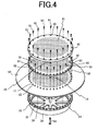
- a probe card 1 according to a first embodiment of the present invention, as shown in FIG. 1 to FIG. 5, is provided with a printed circuit board 10, a stiffener (reinforcing member) 20 provided at the test head side of this printed circuit board 10, upper and lower probe guides 30 and 40 provided at the opposite side to the test head of the printed circuit board 10, and a plurality of contact pins 50 supported by the probe guides 30 and 40.
- This probe card 1 is electrically connected to a test head 110 of a semiconductor wafer test apparatus 100.
- This test head 110 is connected to a tester 120 by a cable.
- a wafer W is held by suction to face this probe card 1 at an alignment system 130 of the semiconductor wafer test apparatus 100.
- This alignment system 130 is designed to be able to make the wafer W move relative to the probe card.
- this semiconductor wafer test apparatus 100 positions the wafer W by the alignment system 130, then brings the contact pins 50 of the probe card 1 into contact with the terminals formed on the wafer W so as to test the semiconductor wafer W.
- the probe guide 30 of this probe card 1 is directly arranged on the printed circuit board 10 at the side (surface) opposite to the test head to form a board side probe guide (below, the "probe guide 30" also being called a “board side probe guide 30").
- the probe guide 40 is stacked over the probe guide 30 and fastened to the probe guide 30 to form a wafer side probe guide (below, the "probe guide 40" also being called a "wafer side probe guide 40").
- the probe guides 30 and 40 are formed with probe areas 31 and 41 corresponding to the tested semiconductor wafer. These probe areas 31 and 41 have pluralities of contact pins 50 arranged corresponding to the arrangements of terminals of the semiconductor wafer.
- the peripheral edge of the board side probe guide 30 is formed with a plurality of through holes 32 through which screws 61 can pass and through holes 33 through which screws 62 can pass alternating with each other. Further, the board side probe guide 30 is formed at its center with a single through hole 34 through which a screw 63 can pass.
- the peripheral edge of the wafer side probe guide 40 is formed with a plurality of through holes 42 through which screws 61 can pass. Further, the wafer side probe guide 40 is formed at its center rear side with a single threaded part 43 with which a screw 63 can be engaged.
- the two probe guide 30 and 40 are, for example, made of ceramic, silicon, glass, or another material. In the present embodiment, they are made of materials having heat expansion coefficients substantially the same as the heat expansion coefficient of the tested semiconductor wafer.
- the printed circuit board 10 in the present embodiment has a thin disk shape having a diameter larger than the probe guides 30 and 40.
- This printed circuit board 10 is formed at the center of its surface with pads 13 as connection terminals to correspond to the arrangement of the terminals of the semiconductor wafer. Further, the printed circuit board 10 is formed at the outer circumference of its rear side with connection terminals 14 for transfer of electrical signals with the test head.
- the printed circuit board 10 is formed with through holes 11 through which screws 61 can pass at positions corresponding to the through holes 32 and 42 of the probe guides 30 and 40.
- the printed circuit board 10 is formed with through holes 12 through which screws 62 can pass at positions corresponding to the through holes 33 of the probe guide 30. These through holes 11 and 12 are formed alternating with each other. Further, the printed circuit board 10 is formed at its center with a single through hole 15 through which a screw 63 can pass.
- the stiffener 20 is provided at the center of the rear of the printed circuit board 10. In the present embodiment, it has an overall substantially dish shape at the peripheral edge of which a flange part 23 is formed.
- This flange part 23 is formed with threaded holes 25 with which the screws 61 can engage at positions corresponding to the threaded holes 32 and 42 of the probe guides 30 and 40.
- the flange part23 is formed with threaded holes 26 with which the screws 62 can engage at positions corresponding to the threaded holes 33 of the probe guide 30. These threaded holes 25 and 26 are alternately formed.
- contact pins 50 in the present embodiment as shown in FIG. 5 and FIG. 6, vertical type spring contact pins (pogo pins) are used.
- Each contact pin 50 is comprised of a cylindrical tube 53, a conductive coil spring 54 housed inside the tube 53, a conductive wafer side plunger 51 biased by the spring force of the coil spring 54 to the wafer side and fastened to the top end of the tube 53, and a conductive board side plunger 52 biased to the board side by the same coil spring 54 and fastened to the bottom end of the tube 53.
- the vertical type contact pins 50 can be handled as independent members, so maintenance is easy.
- the board side probe guide 30 is formed with holding holes 30a for supporting the tubes 53 of the contact pins 50 and holding the board side plungers 52 so as to pass through the board side probe guide 30.
- the wafer side probe guide 40 is formed with support holes 40a for supporting the tubes 53 of the contact pins 50 and guide holes 40a for guiding the wafer side plungers 51 so as to pass through the wafer side probe guide 40.
- the wafer side plunger 51 of each contact pin 50 sticks out a predetermined amount from the guide hole 40b of the wafer side probe guide 40 and is able to elastically retract in the downward direction due to the spring force of the coil spring 54.
- the board side plunger 52 of the contact pin 50 is held in the holding hole 30a of the board side probe guide 30 and in that state is brought into contact with a pad 13 of the printed circuit board 10 by a predetermined contact pressure due to the spring force of the coil spring 54.
- the top end of the tube 53 of the contact pins 50 is biased by the spring force of the coil spring 54 and abuts against the top end face of the support hole 40a in the wafer side probe guide 40. In this way, the wafer side probe guide 40 is given an upward load by the contact pin 50.
- the wafer side plunger 51 of each contact pin 50 is provided with a base material 51a made of for example stainless steel or another special steel, copper alloy, etc. , a first conductive layer 51b with a high hardness, and a second conductive layer 51c with a lower hardness than that first conductive layer 51b.
- the second conductive layer 51c is formed at the outer circumference of the base material 51a, and the first conductive layer 51b is formed in a tube shape so as to tightly contact its outside.
- the front end is worked by for example polishing so that the second conductive layer 51c is exposed.
- the first conductive layer 51b is formed by plating a base material 51a on which the second conductive layer 51c is formed with the first conductive material.
- the first conductive material forming this first conductive layer 51b for example, ruthenium, iridium, rhodium, chromium, nickel, alumite, their alloys or another conductive material with a higher hardness than the oxide film formed on the terminals of the electronic device may be mentioned.
- This first conductive layer 51b has a hardness of at least a Vicker's hardness of 400 Hv, preferably has a hardness of at least a Vicker's hardness of 500 Hv.
- the first conductive layer 51b having this hardness for example, it can effectively break the oxide film (Al 2 O 3 , Vicker's hardness 400 Hv or so) formed on the surface of a general aluminum alloy terminal and the first conductive layer 51b can reach the surface of the terminal of the wafer and electrically contact it.
- the contact pin itself is made of a high hardness material, machining is difficult and the workability is remarkably poor, but in the present embodiment, the base material 51a itself is made of a material superior in workability and is plated on its surface with the first conductive material, so both workability and high hardness can be achieved.
- the second conductive layer 51c is formed by plating etc. the surface of the base material 51a with the second conductive material.
- the second conductive material forming this second conductive layer 51c for example, palladium, nickel, copper, gold, palladium nickel, tin, their alloys or another conductive material with a lower hardness than the oxide film formed on the terminal of the electronic device may be mentioned.
- This second conductive layer 51c has a hardness of not more than a Vicker's hardness of 400 Hv. Due to this, the second conductive layer 51c is more easily worn than the first conductive layer 51b with a large number of pressed contacts, so the first conductive layer 51b projects out in a ring shape at the contact face 50a. That is, since the pushing force easily concentrates at the small area ring shaped first conductive layer 51b, even with a smaller pushing force, the oxide film can be easily broken and the first conductive layer 51b can reach the surface of the terminal of the wafer and electrically contact it. Further, even wi th a large number of pressed contacts, the high hardness first conductive layer 51b enables the contact pin 50 to be maintained in its front end shape, so a contact pin enabling stable electrical contact can be realized.
- the wafer side plunger 51 having this layer structure is tapered thin at its front end. For example, at the initial polishing, polishing paper etc. is used to polish its front end. Both the first conductive layer 51b and second conductive layer 51c are exposed at the front end face 50a of the contact pin 50.
- the high hardness first conductive layer 51b can sharply bite into the terminal to effectively and can break the oxide film formed on the terminal.
- the base material 51a is thickly plated by the second conductive layer 51c so that it is arranged at the inside of the contact pin 50 so that its front end is separated from the front end face 50a of the contact pin 50 by a predetermined distance L (see FIG. 8) .
- the front end of a contact pin 50 gradually becomes worn, but with the contact pin 50 of the present embodiment, the length of the distance L enables the first and second conductive layers 51b and 51c to be newly exposed at the front end face 50a, so the contact pin 50 can be stably maintained in the shape of its front end and can be extended in lifetime.
- the high hardness first conductive layer 51b breaks the oxide film formed on the terminal.
- the ring shape projecting first conductive layer 51b contacting the oxide film is small in area, a smaller pushing force enables breakage.
- the second conductive layer 51c contacts the terminal, but this second conductive layer 51c is low in hardness, so the majority of the pushing force concentrates at the first conductive layer 51b and as a result a small pushing force secures stable contact between the contact pin and terminal.
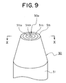
- FIG. 9 and FIG. 10 are views of the front end of a contact pin according to a second embodiment of the present invention.
- the contact pin according to the second embodiment of the present invention is provided with, as a second conductive layer, a total of the three layers of a second outside conductive layer 51c 1 , second intermediate conductive layer 51c 2 , and second inside conductive layer 51c 3 .
- the second outside conductive layer 51c 1 is formed by plating the base material 51a formed with the second intermediate conductive layer 51c 2 and second inside conductive layer 51c 3 with the second conductive material.
- the second intermediate conductive layer 51c 2 is formed by plating the base material 51a formed with the second inside conductive layer 51c 3 with the second conductive material, while the second inside conductive layer 51c 3 is formed by plating the outer circumference of the base material 51a with the second conductive material.
- the second outside conductive layer 51c 1b and the second intermediate conductive layer 51c 2 are both, for example, formed by a combination of layers made of two types of material s selected from palladium, nickel, copper, gold, palladium, nickel, tin, their alloys or another second conductive material and have the same layer structure.
- the second inside conductive layer 51c 3 is made of another type of material from among the above second conductive materials.
- the base material 51a and plating layers are preferably used as combinations of materials with good adhesion.
- the first conductive layer 51b positioned at the outermost layer and projecting out in a ring shape can maintain its mechanical shape with respect to frequent repeated pressing stress.
- the contact pin 50 can be extended in lifetime.
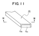
- FIG. 11 and FIG. 12 are view of the front end of a contact pin according to a third embodiment of the present invention.
- the contactpin 70 in this case is for example provided with a base material 70a made of stainless steel or another special steel, copper alloy, etc., a high hardness first conductive layer 70b made of for example ruthenium, iridium, rhodium, chromium, nickel, alumite, or their alloys etc. , and a low hardness second conductive layer 70c made of for example palladium, nickel, copper, gold, palladium nickel, tin, or their alloys.
- the base material 70a is formed on its surface with a second conductive layer 70c by plating etc. and is further formed over that with a first conductive layer 70b by plating etc.
- This contact pin 70 is, for example, polished at the wafer side surface by polishing paper etc. at the time of the initial polishing so that both the first and second conductive layers 70b and 70c are exposed and the first conductive layer 70b and second conductive layer 70c can simultaneously contact the terminal at the time of contact.
Landscapes
- Physics & Mathematics (AREA)
- General Physics & Mathematics (AREA)
- Geometry (AREA)
- Measuring Leads Or Probes (AREA)
- Testing Or Measuring Of Semiconductors Or The Like (AREA)
- Tests Of Electronic Circuits (AREA)
Abstract
A contact pin (50) for contacting a terminal of a wafer and supplying a signal to that wafer is provided with a first conductive layer (51b) composed of a first conductive material having a relatively higher hardness than the oxide film formed on the terminal of the wafer, a second conductive layer (51c) composed of a second conductive material having a relatively lower hardness than the oxide film, and a base material (51a) with the first conductive layer (51b) and second conductive layer (51c) formed at the outside, the first conductive layer (51b) being formed so as to closely contact the outside of the second conductive layer (51c), the first conductive layer (51b) and second conductive layer (51c) both being exposed at the front end face (50a) of the contact pin (50).
Description
- The present invention relates to a contact pin for contacting a terminal of an electronic device and supplying that electronic device with a signal and to a probe card and electronic device test apparatus using the same.
- When producing an IC device or other electronic device having a semiconductor integrated circuit, the integrated circuit is subjected to an operation test not only at the stage of the finished product after dicing, wire bonding, packaging, and other steps (post-process), but also usually at the stage of the semiconductor wafer (pre-process). Due to this, an improvement in the production yield is achieved.
- In a test in this wafer state, a large number of contact pins provided at a probe card are brought into electrical content with the terminals formed in the wafer to transfer electrical signals for testing.
- As the contact pins used for a test in this wafer state, pins obtained by plating a gold alloy or other low hardness metal material on the surface of a base material made of a steel material so as to improve the closeness of contact with the terminals of the wafer at the time of contact have been known in the past.
- However, such contact pins had the problems that since the metal materials are soft, the pins easily deformed upon contact with the terminals and therefore were inferior in terms of durability.
- As opposed to this, as contactpins superior in durability, pins obtained using for example tungsten alloy or another high hardness metal material to make the pins themselves have been known in the past.
- Using, an oxide film is formed over the terminals of a wafer. At the time of contact, the contact pins break this oxide film and reach the terminals themselves. At this time, since such contact pins are overall made of high hardness materials, the area of contact with the oxide film inevitably becomes larger, so there was the problem that the pushing force applied at the time of contact could not efficiently contribute to breakage of the oxide film and stable contact between the contact pins and terminals was difficult to secure. Further, in a probe card having several thousand contact pins, sometimes the pushing force applied at the time of contact with the terminals caused the probe card itself to bend. In such a case, poor contact with the terminals of the wafer easily occurs, so contact pins enabling stable contact with the terminals to be secured with a smaller pushing force have been desired.
- An object of the present invention is to provide a contact pin superior in durability and enabling stable contact with a terminal to be secured with a smaller pushing force and a probe card and electronic device test apparatus using the same.
- To achieve the above object, according to the present invention, there is provided a contact pin for contacting a terminal of an electronic device to supply said electronic device with a signal, provided with a first conductive layer composed of a first conductive material with a high hardness and a second conductive layer composed of a second conductive material with a lower hardness than said first conductive material (see claim 1).
- In the present invention, the first conductive layer composed of the high hardness first conductive material breaks the oxide film formed on the terminal of the electronic device. At this time, in addition to this first conductive layer, by providing a second conductive layer composed of a second conductive material with a lower hardness than the first conductive material, it is possible to make the pushing force applied at the time of contact concentrate at the first conductive layer and possible to secure stable contact between the contact pin and terminal with a small pushing force.
- Further, in the present invention, at the time of contact of the contact pin and terminal, the deformation of the second conductive layer due to the contact is prevented by the high hardness first conductive layer, so superior durability of the contact pin is secured.
- While not particularly limited in the present invention, said first conductive material preferably has a hardness higher than the oxide film formed on the terminal of said electronic device (see claim 2).
- Due to this, the first conductive layer can effectively break the oxide film formed on the terminal of the electronic device to reach the surface of the terminal for electric contact.
- While not particularly limited in the present invention, said second conductive material preferably has a lower hardness than the oxide film formed on the terminal of said electronic device (see claim 3).
- Due to this, the second conductive layer becomes more easily worn than the first conductive layer and, along with a large number of pushing contacts with the terminal, the front end of the contact pin becomes a shape with the first conductive layer sticking out, so the pushing force applied at the time of contact more easily concentrates at the first conductive layer.
- While not particularly limited in the present invention, specifically both said first conductive layer and said second conductive layer preferably are exposed at the front end face of the contact pin at the wafer side (see claim 4).
- While not particularly limited in the present invention, said first conductive layer is preferably formed at the outside from said second conductive layer (see claim 5). More preferably, said first conductive layer is formed so as to be in close contact with the outside of said second conductive layer (see claim 6) .
- By adopting such an arrangement, it is possible to effectively secure stable contact between the contact pin and terminal with a small pushing force.
- While not particularly limited in the present invention, said contact pin preferably is formed finely tapered at its front end (see claim 7).
- Due to this, at the time of contact of the contact pin and terminal, the high hardness first conductive layer can be made to bite into the terminal to effectively break the oxide film.
- While not particularly limited in the present invention, the pin is preferably further provided with a base material at the outside of which the first conductive layer and second conductive layer are formed, said base material being arranged inside said contact pin with the front end of that base material separated by a predetermined distance from the front end of said contact pin (see claim 8).
- Due to this, even if the front end of the contact pin becomes worn, a new first and second conductive layer can be made to be exposed at the surface of the front end, so it is possible to maintain the front end of the contact pin in a stable shape and prolong the pin lifetime.
- While not particularly limited in the present invention, preferably a plurality of at least of said first conductive layer or said second conductive layer is provided (see claim 9).
- Due to this, it is possible to obtain a good adhesion between the conductive layers and mechanical strength, so it is possible to maintain the shape of the front end of the first conductive layer even with a frequent repeated pushing stress and promote the lifetime of the contact pin.
- Further, to achieve the above object, according to the present invention, there is provided a probe card having the above contact pins electrically connected to a test head of an electronic device test apparatus and a board upon one main surface of which said contact pins are provided, said contact pins being brought into contact with terminals of an electronic device to test said electronic device (see claim 10).
- Further, to achieve the above object, according to the present invention, there is provided an electronic device test apparatus having a test head to which the above probe card is electrically connected (see claim 11).
- Due to this, there are provide a probe card and electronic device test apparatus using contact pins superior in durability and enabling stable contact with terminals to be secured with a small pushing force.
-
- [FIG. 1] FIG. 1 is a plan view of a probe card according to a first embodiment of the present invention.
- [FIG. 2] FIG. 2 is a side view of the probe card shown in FIG. 1.
- [FIG. 3] FIG. 3 is a rear view of the probe card shown in FIG. 1.
- [FIG. 4] FIG. 4 is a disassembled perspective view showing the parts of the probe card shown in FIG. 1.
- [FIG. 5] FIG. 5 is a disassembled perspective view showing the basic structure of the probe card shown in FIG. 1.
- [FIG. 6] FIG. 6 is a partial cross-sectional view showing the unit structure of a contact pin.
- [FIG. 7] FIG. 7 is a partial perspective view of the part VII of FIG. 6.
- [FIG. 8] FIG. 8 is a cross-sectional view along the line of VIII-VIII of FIG. 7.
- [FIG. 9] FIG. 9 is a partial perspective view showing the front end of a contact pin according to a second embodiment of the present invention.
- [FIG. 10] FIG. 10 is cross-sectional view along the line X-X of FIG. 9.
- [FIG. 11] FIG. 11 is a partial perspective view showing the front end of a contact pin according to a third embodiment of the present invention.
- [FIG. 12] FIG. 12 is a cross-sectional view along the line XII-XII of FIG. 11.
- Below, embodiments of the present invention will be explained with reference to the drawings.
- A probe card 1 according to a first embodiment of the present invention, as shown in FIG. 1 to FIG. 5, is provided with a printed
circuit board 10, a stiffener (reinforcing member) 20 provided at the test head side of this printedcircuit board 10, upper andlower probe guides circuit board 10, and a plurality ofcontact pins 50 supported by theprobe guides - This probe card 1, as shown in FIG. 5, is electrically connected to a
test head 110 of a semiconductorwafer test apparatus 100. Thistest head 110 is connected to atester 120 by a cable. As opposed to this, a wafer W is held by suction to face this probe card 1 at analignment system 130 of the semiconductorwafer test apparatus 100. Thisalignment system 130 is designed to be able to make the wafer W move relative to the probe card. Further, this semiconductorwafer test apparatus 100 positions the wafer W by thealignment system 130, then brings thecontact pins 50 of the probe card 1 into contact with the terminals formed on the wafer W so as to test the semiconductor wafer W. - The
probe guide 30 of this probe card 1 is directly arranged on the printedcircuit board 10 at the side (surface) opposite to the test head to form a board side probe guide (below, the "probe guide 30" also being called a "boardside probe guide 30"). - As opposed to this, the
probe guide 40 is stacked over theprobe guide 30 and fastened to theprobe guide 30 to form a wafer side probe guide (below, the "probe guide 40" also being called a "waferside probe guide 40"). - The
probe guides probe areas probe areas contact pins 50 arranged corresponding to the arrangements of terminals of the semiconductor wafer. - The peripheral edge of the board
side probe guide 30 is formed with a plurality of throughholes 32 through whichscrews 61 can pass and throughholes 33 through whichscrews 62 can pass alternating with each other. Further, the boardside probe guide 30 is formed at its center with a single throughhole 34 through which ascrew 63 can pass. - The peripheral edge of the wafer
side probe guide 40 is formed with a plurality of throughholes 42 through whichscrews 61 can pass. Further, the waferside probe guide 40 is formed at its center rear side with a single threadedpart 43 with which ascrew 63 can be engaged. - The two
probe guide - The printed
circuit board 10 in the present embodiment has a thin disk shape having a diameter larger than the probe guides 30 and 40. This printedcircuit board 10 is formed at the center of its surface withpads 13 as connection terminals to correspond to the arrangement of the terminals of the semiconductor wafer. Further, the printedcircuit board 10 is formed at the outer circumference of its rear side withconnection terminals 14 for transfer of electrical signals with the test head. - The printed
circuit board 10 is formed with throughholes 11 through which screws 61 can pass at positions corresponding to the throughholes circuit board 10 is formed with throughholes 12 through which screws 62 can pass at positions corresponding to the throughholes 33 of theprobe guide 30. These throughholes circuit board 10 is formed at its center with a single throughhole 15 through which ascrew 63 can pass. - The
stiffener 20 is provided at the center of the rear of the printedcircuit board 10. In the present embodiment, it has an overall substantially dish shape at the peripheral edge of which aflange part 23 is formed. Thisflange part 23 is formed with threadedholes 25 with which thescrews 61 can engage at positions corresponding to the threadedholes holes 26 with which thescrews 62 can engage at positions corresponding to the threadedholes 33 of theprobe guide 30. These threadedholes - Next, the contact pins 50 supported at the two probe guides 30 and 40 will be explained.
- As the contact pins 50 in the present embodiment, as shown in FIG. 5 and FIG. 6, vertical type spring contact pins (pogo pins) are used.
- Each
contact pin 50 is comprised of acylindrical tube 53, aconductive coil spring 54 housed inside thetube 53, a conductivewafer side plunger 51 biased by the spring force of thecoil spring 54 to the wafer side and fastened to the top end of thetube 53, and a conductiveboard side plunger 52 biased to the board side by thesame coil spring 54 and fastened to the bottom end of thetube 53. - The vertical type contact pins 50 can be handled as independent members, so maintenance is easy.
- The board
side probe guide 30 is formed with holdingholes 30a for supporting thetubes 53 of the contact pins 50 and holding theboard side plungers 52 so as to pass through the boardside probe guide 30. Further, the waferside probe guide 40 is formed withsupport holes 40a for supporting thetubes 53 of the contact pins 50 and guideholes 40a for guiding thewafer side plungers 51 so as to pass through the waferside probe guide 40. - The
wafer side plunger 51 of eachcontact pin 50 sticks out a predetermined amount from theguide hole 40b of the waferside probe guide 40 and is able to elastically retract in the downward direction due to the spring force of thecoil spring 54. On the other hand, theboard side plunger 52 of thecontact pin 50 is held in the holdinghole 30a of the boardside probe guide 30 and in that state is brought into contact with apad 13 of the printedcircuit board 10 by a predetermined contact pressure due to the spring force of thecoil spring 54. - In this state, the top end of the
tube 53 of the contact pins 50 is biased by the spring force of thecoil spring 54 and abuts against the top end face of thesupport hole 40a in the waferside probe guide 40. In this way, the waferside probe guide 40 is given an upward load by thecontact pin 50. - Further, the
wafer side plunger 51 of eachcontact pin 50 according to the present embodiment, as shown in FIG. 7 and FIG. 8, is provided with abase material 51a made of for example stainless steel or another special steel, copper alloy, etc. , a first conductive layer 51b with a high hardness, and a secondconductive layer 51c with a lower hardness than that first conductive layer 51b. The secondconductive layer 51c is formed at the outer circumference of thebase material 51a, and the first conductive layer 51b is formed in a tube shape so as to tightly contact its outside. The front end is worked by for example polishing so that the secondconductive layer 51c is exposed. - The first conductive layer 51b is formed by plating a
base material 51a on which the secondconductive layer 51c is formed with the first conductive material. As the first conductive material forming this first conductive layer 51b, for example, ruthenium, iridium, rhodium, chromium, nickel, alumite, their alloys or another conductive material with a higher hardness than the oxide film formed on the terminals of the electronic device may be mentioned. - This first conductive layer 51b has a hardness of at least a Vicker's hardness of 400 Hv, preferably has a hardness of at least a Vicker's hardness of 500 Hv. By the first conductive layer 51b having this hardness, for example, it can effectively break the oxide film (Al2O3, Vicker's hardness 400 Hv or so) formed on the surface of a general aluminum alloy terminal and the first conductive layer 51b can reach the surface of the terminal of the wafer and electrically contact it.
- Note that when the contact pin itself is made of a high hardness material, machining is difficult and the workability is remarkably poor, but in the present embodiment, the
base material 51a itself is made of a material superior in workability and is plated on its surface with the first conductive material, so both workability and high hardness can be achieved. - The second
conductive layer 51c is formed by plating etc. the surface of thebase material 51a with the second conductive material. As the second conductive material forming this secondconductive layer 51c, for example, palladium, nickel, copper, gold, palladium nickel, tin, their alloys or another conductive material with a lower hardness than the oxide film formed on the terminal of the electronic device may be mentioned. - This second
conductive layer 51c has a hardness of not more than a Vicker's hardness of 400 Hv. Due to this, the secondconductive layer 51c is more easily worn than the first conductive layer 51b with a large number of pressed contacts, so the first conductive layer 51b projects out in a ring shape at thecontact face 50a. That is, since the pushing force easily concentrates at the small area ring shaped first conductive layer 51b, even with a smaller pushing force, the oxide film can be easily broken and the first conductive layer 51b can reach the surface of the terminal of the wafer and electrically contact it. Further, even wi th a large number of pressed contacts, the high hardness first conductive layer 51b enables thecontact pin 50 to be maintained in its front end shape, so a contact pin enabling stable electrical contact can be realized. - The
wafer side plunger 51 having this layer structure is tapered thin at its front end. For example, at the initial polishing, polishing paper etc. is used to polish its front end. Both the first conductive layer 51b and secondconductive layer 51c are exposed at thefront end face 50a of thecontact pin 50. - In the present embodiment, by finely tapering the front end of the
contact pin 50, when thecontact pin 50 contacts the terminal, the high hardness first conductive layer 51b can sharply bite into the terminal to effectively and can break the oxide film formed on the terminal. - Further, in the present embodiment, the
base material 51a is thickly plated by the secondconductive layer 51c so that it is arranged at the inside of thecontact pin 50 so that its front end is separated from thefront end face 50a of thecontact pin 50 by a predetermined distance L (see FIG. 8) . - In general, along with the tens of thousands of times of press contact with terminals of wafers, the front end of a
contact pin 50 gradually becomes worn, but with thecontact pin 50 of the present embodiment, the length of the distance L enables the first and secondconductive layers 51b and 51c to be newly exposed at thefront end face 50a, so thecontact pin 50 can be stably maintained in the shape of its front end and can be extended in lifetime. - When a
contact pin 50 of such a configuration contacts a terminal formed on a wafer, first, the high hardness first conductive layer 51b breaks the oxide film formed on the terminal. At this time, since the ring shape projecting first conductive layer 51b contacting the oxide film is small in area, a smaller pushing force enables breakage. At the same time, the secondconductive layer 51c contacts the terminal, but this secondconductive layer 51c is low in hardness, so the majority of the pushing force concentrates at the first conductive layer 51b and as a result a small pushing force secures stable contact between the contact pin and terminal. - Further, at the time of contact between the
contact pin 50 and terminal, deformation of the secondconductive layer 51c due to the contact is prevented by the high hardness first conductive layer 51b, so a superior durability of thecontact pin 50 is secured. - FIG. 9 and FIG. 10 are views of the front end of a contact pin according to a second embodiment of the present invention.
- The contact pin according to the second embodiment of the present invention is provided with, as a second conductive layer, a total of the three layers of a second outside
conductive layer 51c1, second intermediateconductive layer 51c2, and second insideconductive layer 51c3. - The second outside
conductive layer 51c1 is formed by plating thebase material 51a formed with the second intermediateconductive layer 51c2 and second insideconductive layer 51c3 with the second conductive material. Similarly, the second intermediateconductive layer 51c2 is formed by plating thebase material 51a formed with the second insideconductive layer 51c3 with the second conductive material, while the second insideconductive layer 51c3 is formed by plating the outer circumference of thebase material 51a with the second conductive material. - The second outside
conductive layer 51c1b and the second intermediateconductive layer 51c2 are both, for example, formed by a combination of layers made of two types of material s selected from palladium, nickel, copper, gold, palladium, nickel, tin, their alloys or another second conductive material and have the same layer structure. As opposed to this, the second insideconductive layer 51c3 is made of another type of material from among the above second conductive materials. Thebase material 51a and plating layers are preferably used as combinations of materials with good adhesion. - In this way, by providing a plurality of second conductive layers to obtain a good adhesion strength and mechanical strength of the plating layers, the first conductive layer 51b positioned at the outermost layer and projecting out in a ring shape can maintain its mechanical shape with respect to frequent repeated pressing stress. As a result, the
contact pin 50 can be extended in lifetime. - FIG. 11 and FIG. 12 are view of the front end of a contact pin according to a third embodiment of the present invention.
- The configuration explained above is not limited to the vertical type spring contactpin (pogopin) type. As illustrated, it may also be applied to a cantilever contact pin 70 (needle) .
- The
contactpin 70 in this case, like in the first embodiment, is for example provided with a base material 70a made of stainless steel or another special steel, copper alloy, etc., a high hardness firstconductive layer 70b made of for example ruthenium, iridium, rhodium, chromium, nickel, alumite, or their alloys etc. , and a low hardness secondconductive layer 70c made of for example palladium, nickel, copper, gold, palladium nickel, tin, or their alloys. The base material 70a is formed on its surface with a secondconductive layer 70c by plating etc. and is further formed over that with a firstconductive layer 70b by plating etc. - This
contact pin 70 is, for example, polished at the wafer side surface by polishing paper etc. at the time of the initial polishing so that both the first and secondconductive layers conductive layer 70b and secondconductive layer 70c can simultaneously contact the terminal at the time of contact. - Note that the above explained embodiments were described to facilitate understanding of the present invention and were not described to limit the present invention. Therefore the elements disclosed in the above embodiments include all design modifications and equivalents fallingunder the technical scope of the present invention.
Claims (11)
- A contact pin for contacting a terminal of an electronic device to supply said electronic device with a signal, provided with
a first conductive layer composed of a first conductive material with a high hardness and
a second conductive layer composed of a second conductive material with a lower hardness than said first conductive material. - A contact pin as set forth in claim 1, wherein said first conductive material has a hardness higher than the oxide film formed on the terminal of said electronic device.
- A contact pin as set forth in claim 1, wherein said second conductive material has a lower hardness than the oxide film formed on the terminal of said electronic device.
- A contact pin as set forth in claim 1, wherein both said first conductive layer and said second conductive layer are exposed at the front end face of the contact pin at the wafer side.
- A contact pin as set forth in claim 1, wherein said first conductive layer is formed at the outside from said second conductive layer.
- A contact pin as set forth in claim 1, wherein said first conductive layer is formed so as to be in close contact with the outside of said second conductive layer.
- A contact pin as set forth in claim 1 , wherein said contact pin is formed finely tapered at its front end.
- A contact pin as set forth in claim 1, wherein
the pin is further provided with a base material at the outside of which the first conductive layer and second conductive layer are formed,
said base material being arranged inside said contact pin with the front end of that base material separated by a predetermined distance from the front end of said contact pin. - A contact pin as set forth in claim 1, wherein a plurality of at least of said first conductive layer or said second conductive layer is provided.
- A probe card having contact pins of any of claims 1 to 9 electrically connected to a test head of an electronic device test apparatus and a board upon one main surface of which said contact pins are provided, said contact pins being brought into contact with terminals of an electronic device to test said electronic device.
- An electronic device test apparatus having a test head to which a probe card of claim 10 is electrically connected.
Applications Claiming Priority (1)
| Application Number | Priority Date | Filing Date | Title |
|---|---|---|---|
| PCT/JP2004/018652 WO2006064546A1 (en) | 2004-12-14 | 2004-12-14 | Contact pin, probe card using same and electronic device testing apparatus |
Publications (2)
| Publication Number | Publication Date |
|---|---|
| EP1717590A1 true EP1717590A1 (en) | 2006-11-02 |
| EP1717590A4 EP1717590A4 (en) | 2008-10-01 |
Family
ID=36587611
Family Applications (1)
| Application Number | Title | Priority Date | Filing Date |
|---|---|---|---|
| EP04816691A Withdrawn EP1717590A4 (en) | 2004-12-14 | 2004-12-14 | Contact pin, probe card using same and electronic device testing apparatus |
Country Status (5)
| Country | Link |
|---|---|
| US (1) | US7667471B2 (en) |
| EP (1) | EP1717590A4 (en) |
| JP (1) | JPWO2006064546A1 (en) |
| CN (1) | CN100520414C (en) |
| WO (1) | WO2006064546A1 (en) |
Cited By (2)
| Publication number | Priority date | Publication date | Assignee | Title |
|---|---|---|---|---|
| EP2003460A1 (en) * | 2007-06-11 | 2008-12-17 | Micronas GmbH | Pin card assembly |
| ITMI20110896A1 (en) * | 2011-05-20 | 2012-11-21 | Technoprobe Spa | CONTACTING PROBE FOR MEASURING HEAD |
Families Citing this family (26)
| Publication number | Priority date | Publication date | Assignee | Title |
|---|---|---|---|---|
| US9097740B2 (en) * | 2004-05-21 | 2015-08-04 | Formfactor, Inc. | Layered probes with core |
| US9476911B2 (en) | 2004-05-21 | 2016-10-25 | Microprobe, Inc. | Probes with high current carrying capability and laser machining methods |
| US7759949B2 (en) | 2004-05-21 | 2010-07-20 | Microprobe, Inc. | Probes with self-cleaning blunt skates for contacting conductive pads |
| USRE43503E1 (en) | 2006-06-29 | 2012-07-10 | Microprobe, Inc. | Probe skates for electrical testing of convex pad topologies |
| US8988091B2 (en) | 2004-05-21 | 2015-03-24 | Microprobe, Inc. | Multiple contact probes |
| US7728611B1 (en) * | 2006-02-06 | 2010-06-01 | Interconnect Devices, Inc. | Compressive conductors for semiconductor testing |
| JP5028060B2 (en) * | 2006-10-03 | 2012-09-19 | 株式会社アドバンテスト | Performance board and cover material |
| US8907689B2 (en) | 2006-10-11 | 2014-12-09 | Microprobe, Inc. | Probe retention arrangement |
| US7514948B2 (en) | 2007-04-10 | 2009-04-07 | Microprobe, Inc. | Vertical probe array arranged to provide space transformation |
| DE102007040495A1 (en) * | 2007-08-21 | 2009-02-26 | Hansgrohe Ag | plumbing fixture |
| US8723546B2 (en) | 2007-10-19 | 2014-05-13 | Microprobe, Inc. | Vertical guided layered probe |
| JP2009281886A (en) * | 2008-05-22 | 2009-12-03 | Toshiba Corp | Probe card |
| US8230593B2 (en) | 2008-05-29 | 2012-07-31 | Microprobe, Inc. | Probe bonding method having improved control of bonding material |
| EP2322943A4 (en) * | 2008-08-08 | 2014-06-25 | Nhk Spring Co Ltd | ELECTRICAL CONTACT ELEMENT AND CONTACT PROBE |
| JP2011257720A (en) * | 2010-06-04 | 2011-12-22 | Ucm Co Ltd | Camera lens connector |
| US8680844B2 (en) * | 2010-12-01 | 2014-03-25 | General Electric Company | Force compensated probe |
| US8506307B2 (en) | 2010-12-02 | 2013-08-13 | Interconnect Devices, Inc. | Electrical connector with embedded shell layer |
| EP2646839B1 (en) * | 2010-12-03 | 2017-08-16 | Ardent Concepts, Inc. | Compliant electrical contact and assembly |
| US8952711B2 (en) * | 2011-10-20 | 2015-02-10 | Taiwan Semiconductor Manufacturing Company, Ltd. | Methods for probing semiconductor wafers |
| US8933717B2 (en) | 2012-06-21 | 2015-01-13 | International Business Machines Corporation | Probe-on-substrate |
| US9209548B2 (en) * | 2014-04-01 | 2015-12-08 | Interconnect Devices, Inc. | Electrical probe with rotatable plunger |
| JP6237441B2 (en) * | 2014-04-24 | 2017-11-29 | 日本電産リード株式会社 | Electrode structure, inspection jig, and manufacturing method of electrode structure |
| SG11201704433TA (en) * | 2014-12-30 | 2017-07-28 | Technoprobe Spa | Contact probe for testing head |
| US10598696B2 (en) | 2016-03-28 | 2020-03-24 | Intel Corporation | Probe pins with etched tips for electrical die test |
| WO2020158575A1 (en) | 2019-01-29 | 2020-08-06 | 株式会社ヨコオ | Plunger and contact probe |
| KR102893405B1 (en) | 2022-01-13 | 2025-12-02 | 삼성전자주식회사 | Probe card and method for semiconductor device test using the same |
Family Cites Families (19)
| Publication number | Priority date | Publication date | Assignee | Title |
|---|---|---|---|---|
| JP3215452B2 (en) * | 1991-05-30 | 2001-10-09 | 真空冶金株式会社 | Electrode |
| JPH06313774A (en) | 1993-04-30 | 1994-11-08 | Sumitomo Electric Ind Ltd | Method of manufacturing probe |
| US5581083A (en) * | 1995-05-11 | 1996-12-03 | The Regents Of The University Of California | Method for fabricating a sensor on a probe tip used for atomic force microscopy and the like |
| JPH0989930A (en) * | 1995-09-27 | 1997-04-04 | Osaka Diamond Ind Co Ltd | Electronic device contactor and manufacturing method thereof |
| US5986261A (en) * | 1996-04-29 | 1999-11-16 | Nanoptics, Inc. | Tapered structure suitable for microthermocouples microelectrodes, field emission tips and micromagnetic sensors with force sensing capabilities |
| US5923178A (en) * | 1997-04-17 | 1999-07-13 | Cerprobe Corporation | Probe assembly and method for switchable multi-DUT testing of integrated circuit wafers |
| JPH10319039A (en) * | 1997-05-19 | 1998-12-04 | Toshiba Corp | Vertical needle for probe, vertical needle type probe and composite fine wire used for it |
| US5936243A (en) * | 1997-06-09 | 1999-08-10 | Ian Hardcastle | Conductive micro-probe and memory device |
| EP0995996B1 (en) * | 1997-07-14 | 2005-09-07 | Nhk Spring Co.Ltd. | Conductive contact |
| JP3458684B2 (en) | 1997-11-28 | 2003-10-20 | 三菱マテリアル株式会社 | Contact probe |
| JP4880120B2 (en) * | 1998-07-10 | 2012-02-22 | 日本発條株式会社 | Conductive contact |
| JP3745184B2 (en) * | 1999-03-25 | 2006-02-15 | 株式会社東京カソード研究所 | Probe for probe card and manufacturing method thereof |
| JP2000340924A (en) * | 1999-05-27 | 2000-12-08 | Nhk Spring Co Ltd | Probe unit for testing semiconductor chip mounting substrates |
| US6441629B1 (en) | 2000-05-31 | 2002-08-27 | Advantest Corp | Probe contact system having planarity adjustment mechanism |
| FR2814632A1 (en) | 2000-09-27 | 2002-03-29 | Schlumberger Ind Sa | DATA TRANSMISSION METHOD FOR DISTRIBUTION NETWORK COUNTERS |
| JP2002131334A (en) | 2000-10-24 | 2002-05-09 | Nec Yamaguchi Ltd | Probe needle, probe card, and method of manufacturing probe card |
| JP2003014779A (en) | 2001-07-02 | 2003-01-15 | Nhk Spring Co Ltd | Conductive contact |
| WO2003005042A1 (en) * | 2001-07-02 | 2003-01-16 | Nhk Spring Co., Ltd. | Conductive contact |
| US6667629B2 (en) * | 2001-09-24 | 2003-12-23 | Rika Electronics International, Inc. | Electrical test probes and methods of making the same |
-
2004
- 2004-12-14 US US10/566,463 patent/US7667471B2/en not_active Expired - Fee Related
- 2004-12-14 JP JP2006548601A patent/JPWO2006064546A1/en active Pending
- 2004-12-14 CN CN200480019363.4A patent/CN100520414C/en not_active Expired - Fee Related
- 2004-12-14 WO PCT/JP2004/018652 patent/WO2006064546A1/en not_active Ceased
- 2004-12-14 EP EP04816691A patent/EP1717590A4/en not_active Withdrawn
Cited By (3)
| Publication number | Priority date | Publication date | Assignee | Title |
|---|---|---|---|---|
| EP2003460A1 (en) * | 2007-06-11 | 2008-12-17 | Micronas GmbH | Pin card assembly |
| US8125234B2 (en) | 2007-06-11 | 2012-02-28 | Micronas Gmbh | Probe card assembly |
| ITMI20110896A1 (en) * | 2011-05-20 | 2012-11-21 | Technoprobe Spa | CONTACTING PROBE FOR MEASURING HEAD |
Also Published As
| Publication number | Publication date |
|---|---|
| CN1846138A (en) | 2006-10-11 |
| US7667471B2 (en) | 2010-02-23 |
| WO2006064546A1 (en) | 2006-06-22 |
| US20080143366A1 (en) | 2008-06-19 |
| EP1717590A4 (en) | 2008-10-01 |
| JPWO2006064546A1 (en) | 2008-06-12 |
| CN100520414C (en) | 2009-07-29 |
Similar Documents
| Publication | Publication Date | Title |
|---|---|---|
| US7667471B2 (en) | Contact pin probe card and electronic device test apparatus using same | |
| US7479237B2 (en) | Method of fabricating vertical probe head | |
| KR100443999B1 (en) | Interconnector for Printed Circuit Board, method thereby and interconnector assembly having it | |
| US6144212A (en) | Vertical needle type probe card, method of manufacturing thereof, method of replacing defective probe needle and test method of wafer using the probe card | |
| US6830460B1 (en) | Controlled compliance fine pitch interconnect | |
| US7240432B2 (en) | Method of manufacturing a semiconductor device testing contactor having a circuit-side contact piece and test-board-side contact piece | |
| EP2026078A1 (en) | Probe card | |
| US20080030214A1 (en) | Probe head assembly for use in testing multiple wafer die | |
| JPWO2007029422A1 (en) | Semiconductor device inspection device and power supply unit | |
| CN107431317B (en) | Electrical contacts and sockets for electronic components | |
| KR101168147B1 (en) | Probe pin for probe card and manufacturing method thereof | |
| EP1795905A1 (en) | Microcontactor probe and electric probe unit | |
| KR102708649B1 (en) | Supporting plate for electrical test socket, socket pin for electrical test socket, and electrical test socket | |
| CN114207452A (en) | Probe head for electronic device and corresponding probe card | |
| US20090201038A1 (en) | Test head for functional wafer level testing, system and method therefor | |
| KR101890812B1 (en) | Contact pin for test and contact device for test | |
| CN116134322A (en) | Contact probe for probe head | |
| JP5643476B2 (en) | Double elastic mechanism probe card | |
| EP1204988A2 (en) | Controlled compliance fine pitch interconnect | |
| KR100747077B1 (en) | Contact pins, probe cards and electronic component testing equipment using the same | |
| JPH11142438A (en) | Probe and probe card using this probe | |
| JP2009288109A (en) | Double elastic mechanism probe card | |
| US20120132615A1 (en) | Manufacturing method of probe card | |
| KR101149472B1 (en) | A probe card | |
| KR101184364B1 (en) | A probe card pin and a probe card using the same |
Legal Events
| Date | Code | Title | Description |
|---|---|---|---|
| PUAI | Public reference made under article 153(3) epc to a published international application that has entered the european phase |
Free format text: ORIGINAL CODE: 0009012 |
|
| 17P | Request for examination filed |
Effective date: 20060127 |
|
| AK | Designated contracting states |
Kind code of ref document: A1 Designated state(s): AT BE BG CH CY CZ DE DK EE ES FI FR GB GR HU IE IS IT LI LT LU MC NL PL PT RO SE SI SK TR |
|
| AX | Request for extension of the european patent |
Extension state: AL BA HR LV MK YU |
|
| DAX | Request for extension of the european patent (deleted) | ||
| A4 | Supplementary search report drawn up and despatched |
Effective date: 20080903 |
|
| STAA | Information on the status of an ep patent application or granted ep patent |
Free format text: STATUS: THE APPLICATION IS DEEMED TO BE WITHDRAWN |
|
| 18D | Application deemed to be withdrawn |
Effective date: 20110701 |