EP1716446B1 - Dispositif de reglage de la longueur d'une voie optique - Google Patents
Dispositif de reglage de la longueur d'une voie optique Download PDFInfo
- Publication number
- EP1716446B1 EP1716446B1 EP05702995A EP05702995A EP1716446B1 EP 1716446 B1 EP1716446 B1 EP 1716446B1 EP 05702995 A EP05702995 A EP 05702995A EP 05702995 A EP05702995 A EP 05702995A EP 1716446 B1 EP1716446 B1 EP 1716446B1
- Authority
- EP
- European Patent Office
- Prior art keywords
- optical path
- optical
- adjuster
- path length
- input
- Prior art date
- Legal status (The legal status is an assumption and is not a legal conclusion. Google has not performed a legal analysis and makes no representation as to the accuracy of the status listed.)
- Not-in-force
Links
Images


Classifications
-
- G—PHYSICS
- G02—OPTICS
- G02B—OPTICAL ELEMENTS, SYSTEMS OR APPARATUS
- G02B27/00—Optical systems or apparatus not provided for by any of the groups G02B1/00 - G02B26/00, G02B30/00
- G02B27/18—Optical systems or apparatus not provided for by any of the groups G02B1/00 - G02B26/00, G02B30/00 for optical projection, e.g. combination of mirror and condenser and objective
- G02B27/20—Optical systems or apparatus not provided for by any of the groups G02B1/00 - G02B26/00, G02B30/00 for optical projection, e.g. combination of mirror and condenser and objective for imaging minute objects, e.g. light-pointer
-
- G—PHYSICS
- G02—OPTICS
- G02B—OPTICAL ELEMENTS, SYSTEMS OR APPARATUS
- G02B27/00—Optical systems or apparatus not provided for by any of the groups G02B1/00 - G02B26/00, G02B30/00
- G02B27/0025—Optical systems or apparatus not provided for by any of the groups G02B1/00 - G02B26/00, G02B30/00 for optical correction, e.g. distorsion, aberration
- G02B27/0068—Optical systems or apparatus not provided for by any of the groups G02B1/00 - G02B26/00, G02B30/00 for optical correction, e.g. distorsion, aberration having means for controlling the degree of correction, e.g. using phase modulators, movable elements
-
- G—PHYSICS
- G02—OPTICS
- G02B—OPTICAL ELEMENTS, SYSTEMS OR APPARATUS
- G02B27/00—Optical systems or apparatus not provided for by any of the groups G02B1/00 - G02B26/00, G02B30/00
- G02B27/28—Optical systems or apparatus not provided for by any of the groups G02B1/00 - G02B26/00, G02B30/00 for polarising
-
- G—PHYSICS
- G02—OPTICS
- G02B—OPTICAL ELEMENTS, SYSTEMS OR APPARATUS
- G02B30/00—Optical systems or apparatus for producing three-dimensional [3D] effects, e.g. stereoscopic images
- G02B30/50—Optical systems or apparatus for producing three-dimensional [3D] effects, e.g. stereoscopic images the image being built up from image elements distributed over a 3D volume, e.g. voxels
- G02B30/52—Optical systems or apparatus for producing three-dimensional [3D] effects, e.g. stereoscopic images the image being built up from image elements distributed over a 3D volume, e.g. voxels the 3D volume being constructed from a stack or sequence of 2D planes, e.g. depth sampling systems
-
- H—ELECTRICITY
- H04—ELECTRIC COMMUNICATION TECHNIQUE
- H04N—PICTORIAL COMMUNICATION, e.g. TELEVISION
- H04N13/00—Stereoscopic video systems; Multi-view video systems; Details thereof
Definitions
- the present invention relates to methods and apparatus for adjusting an optical path length between two optical elements.
- the invention relates to adjustment of an optical path length within three dimensional display devices that generate a virtual image within a defined imaging volume.
- a three-dimensional image can be created in several ways. For instance, in stereoscopic displays two pictures uniquely observable by each of a viewer's eyes can be shown simultaneously or time-multiplexed. The pictures are selected by means of special spectacles or goggles worn by the viewer. In the former case, the spectacles may be equipped with Polaroid lenses. In the latter case, the spectacles may be equipped with electronically controlled shutters. These types of displays are relatively simple to construct and have a low data-rate. However, the use of special viewing spectacles is inconvenient and the lack of motion parallax may result in discomfort among viewers.
- a more realistic three-dimensional impression can be created using an auto-stereoscopic display.
- every pixel emits light with different intensities in different viewing directions.
- the number of viewing directions should be sufficiently large that each of the viewer's eyes sees a different picture.
- These types of display show a realistic motion parallax; if the viewer's head moves, the view changes accordingly.
- 3D display is a volumetric display as described at http://www.cs.berkley.edu/jfc/MURI/LC-display.
- a volumetric display points in an image display volume emit light. In this way, an image of a three dimensional object can be created.
- a disadvantage of this technique is occlusion, i. e. it is not possible to block the light of points that are hidden by other objects. So, every object displayed is transparent. In principle, this problem can be overcome by means of video-processing and possibly tracking of the position of the viewer's head or eyes.
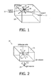
- FIG. 1 A known embodiment of a volumetric display is shown in figure 1 .
- the display consists of a transparent crystal 10 in which two lasers 11,12 (or more) are scanning. At the position 15 of intersection of the laser beams 13, 14, light 16 may be generated by up-conversion, where photon emission at a higher energy occurs by absorption of multiple photons of lower energy (i. e. from the combined laser beams).
- This type of display is expensive and complicated.
- a special crystal 10 and two scanning lasers 11,12 are required.
- up-conversion is not a very efficient process.
- volumetric display 20 An alternative embodiment of volumetric display 20 is shown in figure 2 .
- This arrangement uses a material that can be switched between transparent and diffusive, such as polymer dispersed liquid crystal (PDLC) or liquid crystal gel (LC-gel).
- PDLC polymer dispersed liquid crystal
- LC-gel liquid crystal gel
- cells 22 can be switched between these two states.
- the volume 21 is illuminated from one direction.
- the illumination source 23 is located below the grid volume. If a cell 22 is switched to a diffusive condition, light 24 is scattered in all directions.
- US 4 670 744 discloses a 3D display system in which an optical path length is varied.
- Optical retarders are used to change the polarization of light, and liquid crystal chiral cells are used to provide polarization dependent reflection.
- the location at which reflection takes place can be controlled, thereby adjusting the path length.
- One object of the present invention is to provide a volumetric three dimensional image display device that overcomes some or all of the problems associated with prior art devices.
- Another object of the present invention is to provide an apparatus suitable for adjusting an optical path length between two optical elements within a volumetric three-dimensional image display device.
- a further object of the present invention to provide an optical path length adjuster for varying an optical path length between an input optical path and an output optical path.
- the present invention provides an optical path length adjuster as defined in claim 1.
- the present invention provides a display device as defined in claim 17, and which usesd the optial path length adjuster of the invention.
- the present invention provides a method for varying an optical path length between an input optical path and an output optical path of an optical path length adjuster, as defined in claim 18.
- the present invention provides a method for generating a three-dimensional volumetric image as defined in claim 30, using the method of the invention for varying an optical path length.
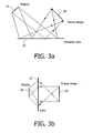
- FIGs 3a and 3b illustrate some basic principles used in a three-dimensional image display device.
- a relatively large virtual image 30 of a small display panel 31 is provided by a Fresnel mirror 32.
- a relatively large virtual image 35 of a small display panel 36 is provided by a Fresnel lens 37.
- the virtual image 30 or 35 appears in the air in front of the lens. A spectator can focus on this image 30 or 35 and observes that it is 'floating' in the air.
- Figures 4a and 4b illustrate a modification to the arrangements of figures 3a and 3b .
- the effective optical path length between the display panel 41 and the Fresnel mirror 42 is varied by the provision of a suitable effective path length adjuster 43.
- the effective optical path length between the display panel 46 and the Fresnel lens 47 is varied by the provision of a suitable effective path length adjuster 48.
- the effective path length adjuster 43, 48 is a variable strength lens; in another arrangement, the effective path length adjuster is a mechanically-driven device which switches between two or more optical paths by physical movement of one or more optical elements.
- the present invention is directed toward electro-optically switching between two or more optical paths thereby avoiding a number of moving parts.
- the mirror 42 or lens 47 may generally be replaced or implemented by any optical focusing element for projecting the two dimensional image of the display panel 41, 46 to a virtual image 40 or 45 located within an imaging volume 44 or 49.
- the mirror 42 or lens 47 is a single or compound optical focusing element having a single focal length such that a planar display panel is imaged into a single plane of an imaging volume.
- Figure 5 illustrates the basic components of the display device 50 according to the principles of figure 4 .
- a two-dimensional display device or 'light engine' 51 provides an illumination source for imaging at an image plane 55.
- the light travels along an input optical path 52 to an optical path length adjuster 53, and from the optical path length adjuster 53 via output optical path 54 to a focusing element 57 (e.g. mirror 42 or lens 47) which projects the two dimensional image to plane 55.
- a focusing element 57 e.g. mirror 42 or lens 47
- Operation of the optical path length adjuster 53 effectively moves the depth position of the image plane 55 as indicated by arrow 58.
- the path length is preferably adjusted periodically at a 3D image display frame frequency. Typically this would be 50 or 60 Hz.
- the virtual image of the display panel 41 or 46 fills the imaging volume 44 or 49.
- the display panel may be driven to alter the image that is projected, so that different depths within the imaging volume 44 or 49 receive different virtual images.
- the path length adjuster 53 is effective to periodically sweep a substantially planar virtual image of the substantially planar two dimensional display panel through the imaging volume 44 or 49 at a 3D frame rate.
- the 2D image display panel displays a succession of 2D images at a 2D frame rate substantially higher than the 3D frame rate.
- the two-dimensional display panel may be any suitable display device for creating a two dimensional image.
- this could be a poly-LED display or a projection display based on a digital micromirror device (DMD).
- DMD digital micromirror device
- the display panel is sufficiently fast to enable the generation of plural 2D images within one frame period of, e.g. 1/50 sec.
- a frame period of, e.g. 1/50 sec For example, commercially available DMDs can reach speeds of 10,000 frames per second. If 24 two-dimensional frames are used to create colour and grey-scale effects and a 3D image refresh rate of 50 Hz is required, it is possible to create eight different image planes 40a, 40b, 45a, 45b in the imaging volume 44, 49.
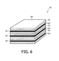
- optical path length adjuster 53 is shown according to a preferred arrangement of the present invention.
- the optical path length adjuster 53 is based on polarising switches 61 and reflective polarisers 62.
- the switches 61 and polarisers 62 are arranged in alternating sequence to form a layered stack 60.
- the expression 'polarisation switch' is used herein to encompass any suitable device for selecting as output a specific polarisation state, e.g. a polarisation rotator that can be switched on and off.
- the polarisation switch 61 may be a single cell liquid crystal panel with a twisted nematic 90 degree structure or a ferro-electric effect cell which allows a higher switching speed.
- the polarisation switch 61 generally provides a polarised optical output in one of two possible polarisation states, according to an applied electric field.
- the expression 'reflective polariser' is used herein to encompass any suitable device that transmits light with one polarisation and reflects light with the other (orthogonal) polarisation.
- reflective polarisers include, but are not limited to, cholesteric polarisers, wire grid polarisers and reflective display films, such as Vikuiti tm film manufactured by 3M (www.3m.com). The former is intended for use with circularly polarised light, while the latter two are for use with linearly polarised light.
- the reflective polariser 62 is a wire grid polariser 62a, 62b, 63c.
- Wire grid polarisers 62a, 62b, 63c have been in use for some time in the microwave region of the electromagnetic spectrum, however, recently wire grid polarisers 62a, 62b, 63c for use in the visible region have been introduced commercially by a company called Moxtek (http://www.moxtek.com).
- Moxtek http://www.moxtek.com
- the theory behind the wire grid polarisers 62a, 62b, 63c is based on electromagnetic induction and wave interference, and is summarised below.
- the function of the wire grid is to allow a light beam incident on the parallel wires having a polarisation state orthogonal to the direction of the wires to be transmitted through the grid. This arises since the electric field of the light beam being orthogonal to the wires cannot generate a significant current in the wires. However, an incident light beam having a polarisation state parallel to the direction of the wires can generate a significant current in the wires to excite electrons in the wires so as to radiate light in both forward and rearward directions. The forward radiated light cancels the light moving in the forward direction and the rearward radiated light emerges as a reflected wave.
- the wire grid polarisers 62a, 62b, 63c are arranged in the stack 60 so as to have parallel planes and such that the direction of the wires are orthogonal to the direction of the wires of a preceding wire grid polariser e.g. 62a and 62b.
- the wire grid polarisers 62a, 62b, 63c are arranged in the stack 60 such that the direction of the wires are parallel to the direction of the wires of a preceding wire grid polariser.
- the switches 61 and polarisers 62 can preferably be mounted on a transparent substrate 63 for stability and support, with the switch/substrate combination 61, 63 forming one type of layer and the polariser/substrate 62, 63 forming another type of layer.
- the substrate 63 can be any suitable rigid and transparent material having a low coefficient of thermal expansion and includes, but is not limited to, glass and Perspex.
- the two types of layers in the stack 60 can either be in contact with adjacent layers or else be spaced apart and separated by an intervening medium such as, but not limited to, air, vacuum or other transparent medium.
- any suitable adhesive or bonding agent which is transparent when set i.e. dry
- any suitable adhesive or bonding agent which is transparent when set i.e. dry
- the layers of the stack may be held together by any suitable mechanical device which operates so as to either permanently or removeably clamp the layers securely together.
- the film typically includes an adhesive layer enabling simple adhesion of the polariser to substrates 63 in the stack 60.
- the stack 60 is constructed with layers which are bonded to each other since the stack 60 is easier to handle and more robust than a separated layer stack. Additionally, the manufacture of a bonded layer stack is easier since the stack can be fabricated as a single device.
- references to 'stack' are taken to refer to both bonded and separated layer stack arrangements, however it is to be understood that the exemplary arrangement is directed to a bonded layer stack 60.
- the stack 60 has a face layer which preferably comprises a polarisation switch. Light is input to the stack 60 along an input optical path 52 which enters the stack 60 through the face layer.
- the lowest layer in the stack 60 is the base layer which operates so as to always reflect incident light.
- this is a plane mirror, but may alternatively be a reflective polariser 62 provided the polarisation state of the incident light on that layer is selected such that reflection will always occur.
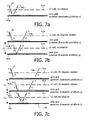
- FIG 7 there is shown a schematic diagram of an exemplary stack arrangement showing possible optical paths within the stack 60.
- the wire grid polarisers 62a, 62b, 62c are arranged so as to have alternating orthogonal wire directions.
- polarisation state S shown as circles on the input path, the circles denoting the electric field vector of the light is normal to the plane of the page.
- the polarisation switch 61 a it is possible to determine the polarisation state of the input beam i.e. to either change or maintain the polarisation state so as to select a preferred polarisation.
- the liquid crystal cell is switched off and so the input beam maintains a polarisation state S after passing through the cell.
- the wire grid polariser 62a is arranged so that the wires run in a direction which is normal to the plane of the page as shown.
- the wire grid polariser 62a acts as a reflector and so the input beam is reflected back from the wire grid polariser 62a and emerges on the output optical path 54a.
- the polarisation state of the incident beam is selected so as to correspond to the direction of the wires of the wire grid polariser 62a, thereby rendering this particular wire grid polariser 62a as the reflecting layer.
- the second wire grid polariser 62b acts as a reflector and so the transmitted beam is reflected back from the second wire grid polariser 62b, passing through the layers 61 b, 62a, 61 a and emerging on the output optical path 54b.
- the polarisation state of the transmitted beam is selected so as to correspond to the direction of the wires of the second wire grid polariser 62b, thereby rendering this particular wire grid polariser 62b as the reflecting layer.
- the input light beam traverses the stack 60 to a greater depth d 1 , thereby varying the optical path length between the input optical path 52 and the output optical path 54b by ⁇ 2d 1 , relative to the first example.
- the example is the same as in figure 7b up to the point where the P-polarised beam transmitted by the first wire grid polariser 62a is incident on the second liquid crystal cell 61 b.
- the second liquid crystal cell 61b is switched on, so the polarisation state of the transmitted beam is changed from P-polarised to S-polarised.
- the second wire grid polariser 62b is arranged such that incident S-polarised light is transmitted, so the S-polarised beam passes through the second wire grid polariser 62b.
- a third liquid crystal cell 61c is switched off, so the polarisation state of the S-polarised transmitted beam is maintained as the beam passes through the cell 61c.
- the third wire grid polariser 62c is arranged so that the wires run in a direction normal to the page as shown and so the polarisation state of the transmitted light beam is parallel to the wire direction.
- the third wire grid polariser 62c acts as a reflector and so the transmitted beam is reflected back from the third wire grid polariser 62c, passing through the layers 61c, 62b, 61b, 62a, 61a and emerging on the output optical path 54c.
- the polarisation state of the transmitted beam is selected so as to correspond to the direction of the wires of the third wire grid polariser 62c, thereby rendering this particular wire grid polariser 62c as the reflecting layer.
- the input light beam traverses the stack to a depth d 1 + d 2 , thereby varying the effective optical path length between the input optical path 52 and the output optical path 54 by a distance ⁇ 2(d 1 + d 2 ), which is further than the optical path length of the second example.
- the distance travelled by an input light beam in passing between two layers spaced by a distance d will be somewhat dependent on the angle of incidence of the beam. Only for normal incidence will the distance travelled be exactly equal to d. For more oblique angles of incidence the distance travelled will be > d.
- the effective optical path length between the input optical path 52 and the output optical path 54 would be equal to 2(d 1 + d 2 ) for normal incidence and would be > 2(d 1 + d 2 ) for increasing angles of incidence.
- the operation of the polarisation switches 61 a, 61 b, 61 c must be adapted accordingly.
- the function of the polarisation switches 61 a, 61 b, 61 c is to select the polarisation state of a beam incident on a particular wire grid polariser, so that the beam is either transmitted or reflected dependent on the direction of the wires.
- the polarisation switches 61a, 61b, 61c provide either 180 degrees or 0 degrees retardation, either changing the handedness of the light beam or else leaving it unchanged at each respective polarisation switch layer.
- the effective optical path length can be increased between the input optical path 52 and the output optical path 54.
- the effective optical path length can be varied by simply selecting a desired depth within the stack 60 at which reflection is to occur from a particular reflective polariser 62. All of this can be achieved without any moving parts.
- the lengths of available optical paths within a particular stack 60 can be pre-selected by choosing the thicknesses of the substrates 63 supporting the polarisation switches 61 and reflective polarisers 62.
- the thicknesses of the substrates 63 may be the same or alternatively may be varied.
- multiple effective optical path lengths within a stack 60 are available by preferably selecting particular combinations of layers having the same or varying thicknesses. Due to the nature of the stack 60 and the operation of the reflective polarisers 62, there is one output optical path 54a, 54b, 54c for each reflective polariser 62a, 62b, 62c.
- Each successive reflective polariser 62a, 62b, 62c gives rise to a respective output optical path 54a, 54b, 54c which is laterally displaced and parallel to the output optical paths 54a, 54b, 54c of the other reflective polarisers 62a, 62b, 62c. This condition does not apply to normal incidence of the input beam however, where output paths are coincident.
- the lengths of available optical paths within a particular stack 60 can be pre-selected by choosing the refractive indices of the substrates 63.
- the refractive indices of the substrates 63 can preferably be the same for all substrates 63 or else be different for different substrates 63.
- the input light beam can be refracted so as to traverse a longer optical path through the substrate 63, relative to another substrate 63 of the same thickness but different refractive index.
- the base layer will only ever receive incident light if each reflective polariser 62 in the stack 60 transmits the light incident on it, or put another way, if none of the reflective polarisers 62 are selected to reflect the incident light.
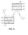
- Further planes 55 can be created by means of more than one adjuster 53 in a cascade arrangement, as shown in figure 8 .
- This is one example of a preferred cascade arrangement comprising two stacks 60a, 60b having opposing face layers.
- one of the many optical paths in the arrangement is defined by selecting the third reflective polariser 62c of the first stack 60a and the first reflective polariser 62d of the second stack 60b to each be reflective.
- the beam can reflect from the selected layers and follow the desired optical path as shown.
- any number of adjusters 53 can be cascaded in this way to provide further effective optical path lengths, leading to further image planes 55.
- stacks 60a, 60b in a cascade arrangement need not be identical in terms of number of layers, substrate thicknesses and refractive indices.
- the different effective optical paths might result in brightness differences due to absorption coefficients of the polarisation switches 61 and/or reflective polarisers 62. This absorption could be compensated for by the intensity of light engine display 51, e.g. corrected electronically in a video signal supplied thereto.
- FIG 9 a schematic view of an overall volumetric image display device using the optical path length adjusters described herein, together with control system, is shown.
- the path length adjuster 120 e.g. adjuster 53 as described earlier
- Path length control circuit 73 provides electrical drive signals to each of the polarisation switches, e.g. 61a, 61 b, 61c.
- a display driver 72 receives 2D frame image data from image generator 71. Display of the succession of 2D images is synchronised with the path length controller operation by way of a synchronisation circuit 74.
- the path length adjuster may have use in other optical instruments and devices, where it is necessary or desirable to facilitate the electro-optical switching of an optical path length between two optical elements.
- Such an arrangement avoids the need for moving parts as the path length can be varied by way of electrical control signals to each of the polarisation switches.
Claims (30)
- Dispositif de réglage de longueur de chemin optique (53) pour faire varier une longueur de chemin optique entre un chemin optique d'entrée (52) et un chemin optique de sortie (54), comprenant : une pluralité de premiers éléments optiques (61) et de deuxièmes éléments optiques (62) agencés successivement en alternance le long d'un chemin optique, chaque premier élément optique pour déterminer un état de polarisation d'un faisceau de lumière traversant cet élément et chaque deuxième élément optique pour transmettre ou réfléchir sélectivement un faisceau de lumière incident sur cet élément en fonction de l'état de polarisation sélectionné du faisceau de lumière incident, dans lequel on peut faire varier la longueur de chemin optique parcourue par un faisceau d'entrée sur le chemin optique en sélectionnant un deuxième élément optique particulier au niveau duquel la réflexion du faisceau d'entrée doit avoir lieu, le faisceau d'entrée réfléchi émergeant le long du chemin optique de sortie ;
caractérisé en ce que le deuxième élément optique (62) comprend un polariseur à grille de fils (62a, 62b, 62c), et en ce que le premier élément optique (61) comprend un commutateur de polarisation (61 a, 61 b, 61 c) sous la forme d'une cellule à cristaux liquides, capable de modifier l'état de polarisation d'un faisceau de lumière traversant l'élément. - Dispositif de réglage suivant la revendication 1, comprenant en outre une pluralité d'écartements différents entre un premier (61) et un deuxième (62) éléments optiques adjacents.
- Dispositif de réglage suivant la revendication 2, dans lequel les écartements entre un premier (61) et un deuxième (62) éléments optiques adjacents ont des épaisseurs différentes en fonction des longueurs de chemin optique requises le long du chemin optique.
- Dispositif de réglage suivant la revendication 2 ou 3, dans lequel les écartements entre un premier (61) et un deuxième (62) éléments optiques adjacents sont occupés par des milieux d'écartement.
- Dispositif de réglage suivant la revendication 4, dans lequel les milieux d'écartement entre un premier (61) et un deuxième (62) éléments optiques adjacents ont des indices de réfraction différents en fonction des longueurs de chemin optique requises le long du chemin optique.
- Dispositif de réglage suivant la revendication 4 ou 5, dans lequel les milieux d'écartement entre un premier (61) et un deuxième (62) éléments optiques adjacents incluent des substrats de verre (63).
- Dispositif de réglage suivant l'une quelconque des revendications précédentes, dans lequel la pluralité de premiers éléments optiques (61) et de deuxièmes éléments optiques (62) sont agencés en une configuration de pile de couches (60).
- Dispositif de réglage suivant la revendication 8, dans lequel le commutateur de polarisation (61 a, 61b, 6 1 c) est supporté par un substrat de verre (63).
- Dispositif de réglage suivant l'une quelconque des revendications précédentes, dans lequel le polariseur à grille de fils (62a, 62b, 62c) est supporté par un substrat de verre (63).
- Dispositif de réglage suivant l'une quelconque des revendications précédentes, dans lequel des polariseurs à grille de fils consécutifs (62a, 62b, 62c) sont agencés de manière à avoir des plans parallèles et de sorte que la direction des fils soit orthogonale par rapport à la direction des fils du polariseur à grille de fils précédent.
- Dispositif de réglage suivant la revendication 7, dans lequel le faisceau d'entrée pénètre la pile (60) à travers une couche de face de la pile, la couche de face étant un desdits premiers éléments optiques (61).
- Dispositif de réglage suivant la revendication 11, dans lequel la pile (60) comporte une couche de base qui est uniquement réflective.
- Dispositif de réglage suivant la revendication 12, dans lequel la couche de base est un miroir plan.
- Dispositif de réglage suivant la revendication 12, dans lequel le faisceau de sortie sort de la pile (60) à travers la couche de face, le faisceau de sortie résultant de la réflexion soit par un deuxième élément optique (62) sélectionné, soit par la couche de base.
- Dispositif de réglage suivant la revendication 1, dans lequel l'écartement (d1, d2) entre des deuxièmes éléments optiques (62) successifs détermine les longueurs de chemin optique possibles le long du chemin optique.
- Dispositif de réglage suivant l'une quelconque des revendications précédentes combiné à au moins un autre dispositif de réglage de longueur de chemin optique suivant l'une quelconque des revendications précédentes en une formation en cascade, de sorte que le chemin optique de sortie (54) du premier dit dispositif de réglage de longueur de chemin optique (53) forme le chemin d'entrée (52) d'un dit autre dispositif de réglage de longueur de chemin optique successif.
- Dispositif d'affichage pour générer une image volumétrique tridimensionnelle, comprenant :un panneau d'affichage d'image bidimensionnelle (41, 46) pour générer une image bidimensionnelle ;un premier élément de focalisation (42, 47) pour projeter l'image bidimensionnelle en une image virtuelle (40, 45) dans un volume d'imagerie (44, 49), etdes moyens (43, 48, 53) pour modifier la longueur de chemin optique effective entre le panneau d'affichage et le premier élément de focalisation de projection de manière à modifier la position de l'image virtuelle dans le volume d'imagerie, dans lequel les moyens pour modifier la longueur de chemin optique effective comprennent le dispositif de réglage de longueur de chemin optique suivant l'une quelconque des revendications 1 à 16.
- Procédé pour faire varier une longueur de chemin optique entre un chemin optique d'entrée (52) et un chemin optique de sortie (54) d'un dispositif de réglage de longueur de chemin optique (53), comprenant les étapes suivantes :la fourniture d'un faisceau de lumière d'entrée sur le chemin optique d'entrée et le passage de celui-ci dans une pluralité de premiers éléments optiques (61) et de deuxièmes éléments optiques (62) agencés successivement en alternance le long du chemin optique ;la détermination d'un état de polarisation du faisceau d'entrée au niveau de chaque premier élément optique que traverse le faisceau, etsoit la transmission, soit la réflexion du faisceau au niveau de chaque deuxième élément optique (62) sur lequel le faisceau est incident, en fonction de l'état de polarisation sélectionné du faisceau incident ; dans lequel on peut faire varier la longueur de chemin optique parcourue par le faisceau d'entrée sur le chemin optique en sélectionnant un deuxième élément optique (62) particulier au niveau duquel la réflexion du faisceau d'entrée doit avoir lieu, le faisceau d'entrée réfléchi émergeant le long du chemin optique de sortie;caractérisé en ce que le deuxième élément optique (62) comprend un polariseur à grille de fils (62a, 62b, 62c) et l'état de polarisation préféré est sélectionné de manière à être parallèle à la direction des fils si le faisceau doit être réfléchi et orthogonal à la direction des fils si le faisceau doit être transmis, et en ce que les premiers éléments optiques comprennent des cellules à cristaux liquides.
- Procédé suivant la revendication 18, dans lequel l'étape de détermination soit change, soit conserve l'état de polarisation du faisceau, de manière à sélectionner un état de polarisation préféré.
- Procédé suivant la revendication 19, dans lequel l'état de polarisation du faisceau est modifié en commutant un commutateur de polarisation (61 a, 61b, 61 c) dans le premier élément optique (61) d'un état de polarisation à un autre état de polarisation.
- Procédé suivant la revendication 19, dans lequel un état de polarisation préféré est sélectionné pour chaque second élément optique (62) sur lequel le faisceau est incident, de manière à correspondre à un état de polarisation qui est soit transmis, soit réfléchi par chaque deuxième élément optique (62) particulier.
- Procédé suivant l'une quelconque des revendications 18 à 21, dans lequel des deuxièmes éléments optiques (62) consécutifs sont agencés de sorte que la direction des fils du polariseur à grille de fils (62a, 62b, 62c) est orthogonale à la direction des fils d'un polariseur à grille de fils précédent.
- Procédé suivant l'une quelconque des revendications 18 à 22, dans lequel la longueur de chemin optique dépend au moins du nombre de deuxièmes éléments optiques (62) qui transmettent le faisceau et des écartements (d1, d2) entre ceux-ci.
- Procédé suivant l'une quelconque des revendications 18 à 23, dans lequel l'agencement de la pluralité de premiers éléments optiques (61) et de deuxièmes éléments optiques (62) successivement en alternance produit une configuration de pile de couches (60), comportant une couche de face correspondant à un premier élément optique et une couche de base qui réfléchit uniquement.
- Procédé suivant la revendication 24, dans lequel l'agencement place les couches en contact les unes avec les autres ou maintient les couches dans un rapport d'espacement.
- Procédé suivant la revendication 24, dans lequel la longueur de chemin optique dépend au moins de la position de la couche dans la pile qui inclut le deuxième élément optique (62) particulier sélectionné pour réfléchir le faisceau.
- Procédé suivant la revendication 26, dans lequel le faisceau est réfléchi par la couche de base si chacun des deuxièmes éléments optiques (62) transmet le faisceau.
- Procédé suivant l'une quelconque des revendications 18 à 27 incluant en outre le passage de la lumière du chemin optique de sortie (54, 54a, 54b, 54c) à un chemin optique d'entrée (52) d'un dispositif de réglage de longueur de chemin optique en aval et la répétition des étapes pour régler la longueur de chemin optique.
- Procédé suivant la revendication 28 incluant en outre l'étape de sélection de longueurs de chemin optique différentes dans chaque dit dispositif de réglage de longueur de chemin optique.
- Procédé de génération d'une image volumétrique tridimensionnelle, comprenant les étapes suivantes :la génération d'une image bidimensionnelle sur un panneau d'affichage d'image bidimensionnelle (41, 46) ;la projection de l'image bidimensionnelle en une image virtuelle (40, 45) dans un volume d'imagerie (44, 49) avec un premier élément de focalisation (42, 47), etla modification de la longueur de chemin optique entre le panneau d'affichage et l'élément de focalisation de projection de manière à faire varier la position de l'image virtuelle dans le volume d'imagerie selon le procédé suivant l'une quelconque des revendications 20 à 29.
Applications Claiming Priority (2)
| Application Number | Priority Date | Filing Date | Title |
|---|---|---|---|
| GBGB0403933.5A GB0403933D0 (en) | 2004-02-21 | 2004-02-21 | Optical path length adjuster |
| PCT/IB2005/050593 WO2005081038A1 (fr) | 2004-02-21 | 2005-02-17 | Dispositif de reglage de la longueur d'une voie optique |
Publications (2)
| Publication Number | Publication Date |
|---|---|
| EP1716446A1 EP1716446A1 (fr) | 2006-11-02 |
| EP1716446B1 true EP1716446B1 (fr) | 2008-02-20 |
Family
ID=32040180
Family Applications (1)
| Application Number | Title | Priority Date | Filing Date |
|---|---|---|---|
| EP05702995A Not-in-force EP1716446B1 (fr) | 2004-02-21 | 2005-02-17 | Dispositif de reglage de la longueur d'une voie optique |
Country Status (10)
| Country | Link |
|---|---|
| US (1) | US20070139760A1 (fr) |
| EP (1) | EP1716446B1 (fr) |
| JP (1) | JP2007529028A (fr) |
| KR (1) | KR20060134066A (fr) |
| CN (1) | CN1922530A (fr) |
| AT (1) | ATE386957T1 (fr) |
| DE (1) | DE602005004895T2 (fr) |
| GB (1) | GB0403933D0 (fr) |
| TW (1) | TW200604619A (fr) |
| WO (1) | WO2005081038A1 (fr) |
Families Citing this family (20)
| Publication number | Priority date | Publication date | Assignee | Title |
|---|---|---|---|---|
| DE102006060604A1 (de) * | 2006-12-21 | 2008-06-26 | Leopold Kostal Gmbh & Co. Kg | Photoelektrische Sensoreinrichtung |
| US8786759B2 (en) | 2007-08-28 | 2014-07-22 | Motorola Mobility Llc | Method and apparatus for auto-focus using liquid crystal adaptive optics |
| US7933509B2 (en) | 2007-12-31 | 2011-04-26 | Motorola, Inc. | Device and method for reducing optical blurring |
| TWI452549B (zh) * | 2011-10-12 | 2014-09-11 | Univ Southern Taiwan | 結合虛擬影像之實物懸浮展示構造 |
| US8717425B2 (en) | 2011-11-18 | 2014-05-06 | Leslie C. Hardison | System for stereoscopically viewing motion pictures |
| CN103984055A (zh) * | 2014-05-09 | 2014-08-13 | 京东方科技集团股份有限公司 | 一种偏光结构及其制作方法、显示面板 |
| US10254551B2 (en) * | 2014-06-13 | 2019-04-09 | Mitsubishi Electric Corporation | Virtual image display device |
| KR101615239B1 (ko) | 2014-10-06 | 2016-04-25 | 엘지전자 주식회사 | 공간 영상 투영 장치 |
| US10379388B2 (en) | 2016-08-12 | 2019-08-13 | Avegant Corp. | Digital light path length modulation systems |
| US10057488B2 (en) | 2016-08-12 | 2018-08-21 | Avegant Corp. | Image capture with digital light path length modulation |
| US10187634B2 (en) | 2016-08-12 | 2019-01-22 | Avegant Corp. | Near-eye display system including a modulation stack |
| US10516879B2 (en) | 2016-08-12 | 2019-12-24 | Avegant Corp. | Binocular display with digital light path length modulation |
| US10401639B2 (en) | 2016-08-12 | 2019-09-03 | Avegant Corp. | Method and apparatus for an optical path length extender |
| US10809546B2 (en) | 2016-08-12 | 2020-10-20 | Avegant Corp. | Digital light path length modulation |
| WO2018031965A1 (fr) | 2016-08-12 | 2018-02-15 | Avegant Corp. | Modulation numérique de longueur de trajet de lumière |
| US10185153B2 (en) | 2016-08-12 | 2019-01-22 | Avegant Corp. | Orthogonal optical path length extender |
| TWI617845B (zh) | 2017-03-16 | 2018-03-11 | 財團法人工業技術研究院 | 影像感測裝置 |
| CN112771436B (zh) * | 2019-08-26 | 2023-10-20 | 京东方科技集团股份有限公司 | 三维显示装置及虚拟现实设备 |
| CN111221143B (zh) * | 2020-01-19 | 2022-03-11 | 平行现实(杭州)科技有限公司 | 基于折叠光路和液晶盒的变光程三维虚拟现实显示装置及显示方法 |
| CN114779494B (zh) * | 2022-06-17 | 2022-09-02 | 深圳市文生科技有限公司 | 成像元件及成像装置 |
Family Cites Families (26)
| Publication number | Priority date | Publication date | Assignee | Title |
|---|---|---|---|---|
| US3645604A (en) * | 1970-08-10 | 1972-02-29 | Bell Telephone Labor Inc | Liquid crystal display |
| DE3313217A1 (de) * | 1983-04-13 | 1984-10-18 | Bruker Medizintechnik Gmbh, 7512 Rheinstetten | Einrichtung zum erzeugen vollstaendiger dreidimensionaler darstellungen eines raeumlichen objektes |
| US4878741A (en) * | 1986-09-10 | 1989-11-07 | Manchester R & D Partnership | Liquid crystal color display and method |
| US4670744A (en) * | 1985-03-14 | 1987-06-02 | Tektronix, Inc. | Light reflecting three-dimensional display system |
| CA1278080C (fr) * | 1986-08-20 | 1990-12-18 | Yasuo Yamagishi | Dispositif d'affichage couleur a cristaux liquides du type a projection |
| US5383053A (en) * | 1992-04-07 | 1995-01-17 | Hughes Aircraft Company | Virtual image display having a high efficiency grid beamsplitter |
| US5686979A (en) * | 1995-06-26 | 1997-11-11 | Minnesota Mining And Manufacturing Company | Optical panel capable of switching between reflective and transmissive states |
| US5978125A (en) * | 1995-11-30 | 1999-11-02 | Yao; X. Steve | Compact programmable photonic variable delay devices |
| US5841494A (en) * | 1996-06-26 | 1998-11-24 | Hall; Dennis R. | Transflective LCD utilizing chiral liquid crystal filter/mirrors |
| GB2317710A (en) * | 1996-09-27 | 1998-04-01 | Sharp Kk | Spatial light modulator and directional display |
| US5920411A (en) * | 1997-02-14 | 1999-07-06 | Duck; Gary S. | Optical multiplexing/demultiplexing device |
| JP3702643B2 (ja) * | 1997-06-09 | 2005-10-05 | セイコーエプソン株式会社 | 表示装置及び電子時計 |
| US6108131A (en) * | 1998-05-14 | 2000-08-22 | Moxtek | Polarizer apparatus for producing a generally polarized beam of light |
| US6459467B1 (en) * | 1998-05-15 | 2002-10-01 | Minolta Co., Ltd. | Liquid crystal light modulating device, and a manufacturing method and a manufacturing apparatus thereof |
| US6081376A (en) * | 1998-07-16 | 2000-06-27 | Moxtek | Reflective optical polarizer device with controlled light distribution and liquid crystal display incorporating the same |
| JP2000050314A (ja) * | 1998-07-27 | 2000-02-18 | Citizen Watch Co Ltd | 立体表示装置 |
| US5986730A (en) * | 1998-12-01 | 1999-11-16 | Moxtek | Dual mode reflective/transmissive liquid crystal display apparatus |
| US6781666B2 (en) * | 1999-07-16 | 2004-08-24 | Minolta Co., Ltd. | Liquid crystal display and method to manufacture the same |
| US6447120B2 (en) * | 1999-07-28 | 2002-09-10 | Moxtex | Image projection system with a polarizing beam splitter |
| US6234634B1 (en) * | 1999-07-28 | 2001-05-22 | Moxtek | Image projection system with a polarizing beam splitter |
| US6812977B1 (en) * | 1999-11-22 | 2004-11-02 | Minolta Co., Ltd. | Liquid crystal element |
| US6356323B1 (en) * | 2000-08-11 | 2002-03-12 | Eastman Kodak Company | Color display using cholesteric liquid crystals |
| NZ514500A (en) * | 2001-10-11 | 2004-06-25 | Deep Video Imaging Ltd | A multiplane visual display unit with a transparent emissive layer disposed between two display planes |
| US7394506B2 (en) * | 2002-07-08 | 2008-07-01 | Koninklijke Philips Electronics N.V. | Reflective stereoscopic display with first and second liquid crystal cells |
| WO2007044028A2 (fr) * | 2004-11-30 | 2007-04-19 | Agoura Technologies, Inc. | Applications et techniques de fabrication de polariseurs a grille de grande dimension |
| KR100647311B1 (ko) * | 2005-01-26 | 2006-11-23 | 삼성전자주식회사 | 집적형 광학필터장치 |
-
2004
- 2004-02-21 GB GBGB0403933.5A patent/GB0403933D0/en not_active Ceased
-
2005
- 2005-02-17 JP JP2006553750A patent/JP2007529028A/ja active Pending
- 2005-02-17 KR KR1020067016527A patent/KR20060134066A/ko not_active Application Discontinuation
- 2005-02-17 DE DE602005004895T patent/DE602005004895T2/de active Active
- 2005-02-17 EP EP05702995A patent/EP1716446B1/fr not_active Not-in-force
- 2005-02-17 US US10/598,019 patent/US20070139760A1/en not_active Abandoned
- 2005-02-17 CN CNA2005800053046A patent/CN1922530A/zh active Pending
- 2005-02-17 WO PCT/IB2005/050593 patent/WO2005081038A1/fr active IP Right Grant
- 2005-02-17 AT AT05702995T patent/ATE386957T1/de not_active IP Right Cessation
- 2005-02-18 TW TW094104907A patent/TW200604619A/zh unknown
Also Published As
| Publication number | Publication date |
|---|---|
| US20070139760A1 (en) | 2007-06-21 |
| KR20060134066A (ko) | 2006-12-27 |
| JP2007529028A (ja) | 2007-10-18 |
| WO2005081038A1 (fr) | 2005-09-01 |
| DE602005004895D1 (de) | 2008-04-03 |
| GB0403933D0 (en) | 2004-03-24 |
| EP1716446A1 (fr) | 2006-11-02 |
| TW200604619A (en) | 2006-02-01 |
| ATE386957T1 (de) | 2008-03-15 |
| CN1922530A (zh) | 2007-02-28 |
| DE602005004895T2 (de) | 2009-02-12 |
Similar Documents
| Publication | Publication Date | Title |
|---|---|---|
| EP1716446B1 (fr) | Dispositif de reglage de la longueur d'une voie optique | |
| EP1706778B1 (fr) | Afficheur tridimensionnel avec un dispositif de reglage de la longueur d'un trajet optique | |
| US7375885B2 (en) | Autostereoscopic display | |
| EP1950980B1 (fr) | Appareil d'affichage autostéreoscopique commutable en 2D/3D et hautement efficace, utilisant un écran gaufré et un multiplexage temporel des vues 3D | |
| JP3990984B2 (ja) | 遠視野ディスプレイ | |
| US20080192111A1 (en) | Volumetric Display | |
| JP6714514B2 (ja) | ホログラフィック光学素子を使用する裸眼立体視3d表示装置 | |
| EP0508824B1 (fr) | Appareil d'affichage d'images tridimensionnelles | |
| US20140118825A1 (en) | Stereoscopic image display apparatus and stereoscopic image display method | |
| US9291830B2 (en) | Multiview projector system | |
| KR20080086110A (ko) | 고효율 2차원/3차원 겸용 영상 표시장치 | |
| JPH1063199A (ja) | 液晶表示装置 | |
| JP2000047138A (ja) | 画像表示装置 | |
| JP2007526499A (ja) | 複屈折性光路長調節器を使用した体積測定画像化ディスプレイ装置 | |
| US11662591B1 (en) | Display systems and imaging systems with dynamically controllable optical path lengths | |
| KR20130021868A (ko) | 입체영상 표시장치 | |
| JP2002010298A (ja) | 三次元表示装置 | |
| US20240004215A1 (en) | Full lightfield with monocular and stereoscopic depth control via monocular-to-binocular hybridization | |
| US20240004195A1 (en) | Wearable device with 1d-1d optical surfaces for stereoscopic and monocular depth programming | |
| JP4021267B2 (ja) | 立体視画像投影用光学エレメント及びそれを組み込んだプロジェクタ | |
| JP2024006899A (ja) | 立体視および単眼の深さプログラミングを備えたヴィークル車載用ディスプレイ | |
| CN117452648A (zh) | 一种ar眼镜 | |
| JP2000175220A (ja) | 三次元表示方法及び装置 |
Legal Events
| Date | Code | Title | Description |
|---|---|---|---|
| PUAI | Public reference made under article 153(3) epc to a published international application that has entered the european phase |
Free format text: ORIGINAL CODE: 0009012 |
|
| 17P | Request for examination filed |
Effective date: 20060704 |
|
| AK | Designated contracting states |
Kind code of ref document: A1 Designated state(s): AT BE BG CH CY CZ DE DK EE ES FI FR GB GR HU IE IS IT LI LT LU MC NL PL PT RO SE SI SK TR |
|
| 17Q | First examination report despatched |
Effective date: 20061208 |
|
| DAX | Request for extension of the european patent (deleted) | ||
| GRAP | Despatch of communication of intention to grant a patent |
Free format text: ORIGINAL CODE: EPIDOSNIGR1 |
|
| GRAS | Grant fee paid |
Free format text: ORIGINAL CODE: EPIDOSNIGR3 |
|
| GRAA | (expected) grant |
Free format text: ORIGINAL CODE: 0009210 |
|
| AK | Designated contracting states |
Kind code of ref document: B1 Designated state(s): AT BE BG CH CY CZ DE DK EE ES FI FR GB GR HU IE IS IT LI LT LU MC NL PL PT RO SE SI SK TR |
|
| REG | Reference to a national code |
Ref country code: GB Ref legal event code: FG4D |
|
| REG | Reference to a national code |
Ref country code: CH Ref legal event code: EP |
|
| REG | Reference to a national code |
Ref country code: IE Ref legal event code: FG4D |
|
| REF | Corresponds to: |
Ref document number: 602005004895 Country of ref document: DE Date of ref document: 20080403 Kind code of ref document: P |
|
| REG | Reference to a national code |
Ref country code: GB Ref legal event code: 746 Effective date: 20080425 |
|
| PG25 | Lapsed in a contracting state [announced via postgrant information from national office to epo] |
Ref country code: IS Free format text: LAPSE BECAUSE OF FAILURE TO SUBMIT A TRANSLATION OF THE DESCRIPTION OR TO PAY THE FEE WITHIN THE PRESCRIBED TIME-LIMIT Effective date: 20080620 Ref country code: FI Free format text: LAPSE BECAUSE OF FAILURE TO SUBMIT A TRANSLATION OF THE DESCRIPTION OR TO PAY THE FEE WITHIN THE PRESCRIBED TIME-LIMIT Effective date: 20080220 Ref country code: ES Free format text: LAPSE BECAUSE OF FAILURE TO SUBMIT A TRANSLATION OF THE DESCRIPTION OR TO PAY THE FEE WITHIN THE PRESCRIBED TIME-LIMIT Effective date: 20080531 |
|
| NLV1 | Nl: lapsed or annulled due to failure to fulfill the requirements of art. 29p and 29m of the patents act | ||
| PG25 | Lapsed in a contracting state [announced via postgrant information from national office to epo] |
Ref country code: AT Free format text: LAPSE BECAUSE OF FAILURE TO SUBMIT A TRANSLATION OF THE DESCRIPTION OR TO PAY THE FEE WITHIN THE PRESCRIBED TIME-LIMIT Effective date: 20080220 |
|
| PG25 | Lapsed in a contracting state [announced via postgrant information from national office to epo] |
Ref country code: SI Free format text: LAPSE BECAUSE OF FAILURE TO SUBMIT A TRANSLATION OF THE DESCRIPTION OR TO PAY THE FEE WITHIN THE PRESCRIBED TIME-LIMIT Effective date: 20080220 Ref country code: PL Free format text: LAPSE BECAUSE OF FAILURE TO SUBMIT A TRANSLATION OF THE DESCRIPTION OR TO PAY THE FEE WITHIN THE PRESCRIBED TIME-LIMIT Effective date: 20080220 Ref country code: BE Free format text: LAPSE BECAUSE OF FAILURE TO SUBMIT A TRANSLATION OF THE DESCRIPTION OR TO PAY THE FEE WITHIN THE PRESCRIBED TIME-LIMIT Effective date: 20080220 |
|
| PG25 | Lapsed in a contracting state [announced via postgrant information from national office to epo] |
Ref country code: DK Free format text: LAPSE BECAUSE OF FAILURE TO SUBMIT A TRANSLATION OF THE DESCRIPTION OR TO PAY THE FEE WITHIN THE PRESCRIBED TIME-LIMIT Effective date: 20080220 Ref country code: CZ Free format text: LAPSE BECAUSE OF FAILURE TO SUBMIT A TRANSLATION OF THE DESCRIPTION OR TO PAY THE FEE WITHIN THE PRESCRIBED TIME-LIMIT Effective date: 20080220 Ref country code: PT Free format text: LAPSE BECAUSE OF FAILURE TO SUBMIT A TRANSLATION OF THE DESCRIPTION OR TO PAY THE FEE WITHIN THE PRESCRIBED TIME-LIMIT Effective date: 20080721 Ref country code: SE Free format text: LAPSE BECAUSE OF FAILURE TO SUBMIT A TRANSLATION OF THE DESCRIPTION OR TO PAY THE FEE WITHIN THE PRESCRIBED TIME-LIMIT Effective date: 20080520 Ref country code: NL Free format text: LAPSE BECAUSE OF FAILURE TO SUBMIT A TRANSLATION OF THE DESCRIPTION OR TO PAY THE FEE WITHIN THE PRESCRIBED TIME-LIMIT Effective date: 20080220 Ref country code: SK Free format text: LAPSE BECAUSE OF FAILURE TO SUBMIT A TRANSLATION OF THE DESCRIPTION OR TO PAY THE FEE WITHIN THE PRESCRIBED TIME-LIMIT Effective date: 20080220 |
|
| ET | Fr: translation filed | ||
| PG25 | Lapsed in a contracting state [announced via postgrant information from national office to epo] |
Ref country code: RO Free format text: LAPSE BECAUSE OF FAILURE TO SUBMIT A TRANSLATION OF THE DESCRIPTION OR TO PAY THE FEE WITHIN THE PRESCRIBED TIME-LIMIT Effective date: 20080220 |
|
| PLBE | No opposition filed within time limit |
Free format text: ORIGINAL CODE: 0009261 |
|
| STAA | Information on the status of an ep patent application or granted ep patent |
Free format text: STATUS: NO OPPOSITION FILED WITHIN TIME LIMIT |
|
| 26N | No opposition filed |
Effective date: 20081121 |
|
| PG25 | Lapsed in a contracting state [announced via postgrant information from national office to epo] |
Ref country code: LT Free format text: LAPSE BECAUSE OF FAILURE TO SUBMIT A TRANSLATION OF THE DESCRIPTION OR TO PAY THE FEE WITHIN THE PRESCRIBED TIME-LIMIT Effective date: 20080220 |
|
| PG25 | Lapsed in a contracting state [announced via postgrant information from national office to epo] |
Ref country code: EE Free format text: LAPSE BECAUSE OF FAILURE TO SUBMIT A TRANSLATION OF THE DESCRIPTION OR TO PAY THE FEE WITHIN THE PRESCRIBED TIME-LIMIT Effective date: 20080220 Ref country code: BG Free format text: LAPSE BECAUSE OF FAILURE TO SUBMIT A TRANSLATION OF THE DESCRIPTION OR TO PAY THE FEE WITHIN THE PRESCRIBED TIME-LIMIT Effective date: 20080520 |
|
| PG25 | Lapsed in a contracting state [announced via postgrant information from national office to epo] |
Ref country code: CY Free format text: LAPSE BECAUSE OF FAILURE TO SUBMIT A TRANSLATION OF THE DESCRIPTION OR TO PAY THE FEE WITHIN THE PRESCRIBED TIME-LIMIT Effective date: 20080220 |
|
| PG25 | Lapsed in a contracting state [announced via postgrant information from national office to epo] |
Ref country code: IT Free format text: LAPSE BECAUSE OF FAILURE TO SUBMIT A TRANSLATION OF THE DESCRIPTION OR TO PAY THE FEE WITHIN THE PRESCRIBED TIME-LIMIT Effective date: 20080220 |
|
| PG25 | Lapsed in a contracting state [announced via postgrant information from national office to epo] |
Ref country code: MC Free format text: LAPSE BECAUSE OF NON-PAYMENT OF DUE FEES Effective date: 20090228 |
|
| REG | Reference to a national code |
Ref country code: CH Ref legal event code: PL |
|
| PG25 | Lapsed in a contracting state [announced via postgrant information from national office to epo] |
Ref country code: LI Free format text: LAPSE BECAUSE OF NON-PAYMENT OF DUE FEES Effective date: 20090228 Ref country code: CH Free format text: LAPSE BECAUSE OF NON-PAYMENT OF DUE FEES Effective date: 20090228 |
|
| PG25 | Lapsed in a contracting state [announced via postgrant information from national office to epo] |
Ref country code: IE Free format text: LAPSE BECAUSE OF NON-PAYMENT OF DUE FEES Effective date: 20090217 |
|
| PGFP | Annual fee paid to national office [announced via postgrant information from national office to epo] |
Ref country code: FR Payment date: 20100311 Year of fee payment: 6 |
|
| PGFP | Annual fee paid to national office [announced via postgrant information from national office to epo] |
Ref country code: GB Payment date: 20100226 Year of fee payment: 6 |
|
| PGFP | Annual fee paid to national office [announced via postgrant information from national office to epo] |
Ref country code: DE Payment date: 20100430 Year of fee payment: 6 |
|
| PG25 | Lapsed in a contracting state [announced via postgrant information from national office to epo] |
Ref country code: GR Free format text: LAPSE BECAUSE OF FAILURE TO SUBMIT A TRANSLATION OF THE DESCRIPTION OR TO PAY THE FEE WITHIN THE PRESCRIBED TIME-LIMIT Effective date: 20080521 |
|
| PG25 | Lapsed in a contracting state [announced via postgrant information from national office to epo] |
Ref country code: LU Free format text: LAPSE BECAUSE OF NON-PAYMENT OF DUE FEES Effective date: 20090217 |
|
| PG25 | Lapsed in a contracting state [announced via postgrant information from national office to epo] |
Ref country code: HU Free format text: LAPSE BECAUSE OF FAILURE TO SUBMIT A TRANSLATION OF THE DESCRIPTION OR TO PAY THE FEE WITHIN THE PRESCRIBED TIME-LIMIT Effective date: 20080821 |
|
| PG25 | Lapsed in a contracting state [announced via postgrant information from national office to epo] |
Ref country code: TR Free format text: LAPSE BECAUSE OF FAILURE TO SUBMIT A TRANSLATION OF THE DESCRIPTION OR TO PAY THE FEE WITHIN THE PRESCRIBED TIME-LIMIT Effective date: 20080220 |
|
| GBPC | Gb: european patent ceased through non-payment of renewal fee |
Effective date: 20110217 |
|
| REG | Reference to a national code |
Ref country code: FR Ref legal event code: ST Effective date: 20111102 |
|
| REG | Reference to a national code |
Ref country code: DE Ref legal event code: R119 Ref document number: 602005004895 Country of ref document: DE Effective date: 20110901 |
|
| PG25 | Lapsed in a contracting state [announced via postgrant information from national office to epo] |
Ref country code: FR Free format text: LAPSE BECAUSE OF NON-PAYMENT OF DUE FEES Effective date: 20110228 |
|
| PG25 | Lapsed in a contracting state [announced via postgrant information from national office to epo] |
Ref country code: GB Free format text: LAPSE BECAUSE OF NON-PAYMENT OF DUE FEES Effective date: 20110217 |
|
| PG25 | Lapsed in a contracting state [announced via postgrant information from national office to epo] |
Ref country code: DE Free format text: LAPSE BECAUSE OF NON-PAYMENT OF DUE FEES Effective date: 20110901 |