EP1708302B1 - Schaltung mit verteilten Parametern und Verfahren zur Impedanzanpassung - Google Patents
Schaltung mit verteilten Parametern und Verfahren zur Impedanzanpassung Download PDFInfo
- Publication number
- EP1708302B1 EP1708302B1 EP06005190A EP06005190A EP1708302B1 EP 1708302 B1 EP1708302 B1 EP 1708302B1 EP 06005190 A EP06005190 A EP 06005190A EP 06005190 A EP06005190 A EP 06005190A EP 1708302 B1 EP1708302 B1 EP 1708302B1
- Authority
- EP
- European Patent Office
- Prior art keywords
- impedance
- line
- micro strip
- strip line
- adjustment
- Prior art date
- Legal status (The legal status is an assumption and is not a legal conclusion. Google has not performed a legal analysis and makes no representation as to the accuracy of the status listed.)
- Expired - Fee Related
Links
Images


Classifications
-
- H—ELECTRICITY
- H01—ELECTRIC ELEMENTS
- H01P—WAVEGUIDES; RESONATORS, LINES, OR OTHER DEVICES OF THE WAVEGUIDE TYPE
- H01P3/00—Waveguides; Transmission lines of the waveguide type
- H01P3/02—Waveguides; Transmission lines of the waveguide type with two longitudinal conductors
- H01P3/08—Microstrips; Strip lines
- H01P3/081—Microstriplines
Definitions
- the present invention relates to a distributed constant circuit capable of achieving impedance matching between a conductor line provided on the top face of a substrate and an electronic device connected to an input terminal or an output terminal and a method of adjusting the impedance matching of the distributed constant circuit.
- FIG. 1 shows a distributed constant circuit in which the adjustment pads are formed.
- reference numeral 10 denotes a substrate
- reference numerals 11, 12 denote a micro strip line
- reference numeral 15 denotes an input terminal to the micro strip line
- reference numeral 16 denotes an output terminal from a micro strip line
- reference numeral 17 denotes a ground
- reference numeral 21 denotes a semiconductor device
- reference numerals 51, 52 denote adjustment pads
- reference numeral 500 denotes a distributed constant circuit.
- the micro strip lines 11, 12 are designed so as to have an inherent characteristic impedance.
- the semiconductor device 21 is designed so as to have inherent load impedance on the input side of the semiconductor device 21 and an inherent drive impedance on the output side.
- the characteristic impedance of the micro strip line 11 and the load impedance of the semiconductor 21 are set up to match each other and the characteristic impedance of the micro strip line 12 and the drive impedance of the semiconductor device 21 are set up to match each other.
- the micro strip line 11 and the adjustment pad 51 are connected with metal wire, solder and metal plate so as to achieve matching between the characteristic impedance of the micro strip 11 and the load impedance of the semiconductor device 21 and then, the micro strip line 12 and the adjustment pads 52 are connected so as to achieve matching between the characteristic impedance of the micro strip line 12 and the drive impedance of the semiconductor device 21.
- the conventional art described in FIG. 1 needs a large number of adjustment pads if the impedance mismatching is large or the characteristic impedance is low.
- the large number of the adjustment pads requires a wide area for arrangement of the adjustment pads preliminarily. Occupation of a wide area increases the size of the distributed constant circuit. Further, interference with other distributed constant circuit is generated. Further, because the adjustment pad and the micro strip line are coupled even when they are not connected with any metal wire or the like, the characteristic impedance becomes different from that of a single unit micro strip line only by disposing the adjustment pads.
- Japanese Laid Open Publication 58094201 discloses an impedance matching member, which increases reliability by including a controlling strip line in the impedance matching member having the prescribed specific impedance and pressing the strip line to its symmetric strip line to secure a face contact between these two lines.
- US 6,101,295 discloses a high-frequency circuit provided with a microstrip line, an optical semiconductor element located at the tip of the microstrip line, and open stubs joined to the microstrip line.
- the stubs and the section of the microstrip line to which the stubs are joined constitute a matching circuit. Impedance matching between the high frequency circuit and an external circuit is achieved by means of this matching circuit.
- US 7,701,727 discloses a stripline tapped-line hairpin filter. Hairpin resonators are located alternately on opposite surfaces of a substrate. The first and last hairpin resonators are tapped to permit signal input and output of the filter, with the hairpin resonator carrying substrate being sandwiched between two groundplanes insulated therefrom by a pair of dielectric substrates.
- Japanese Laid Open Publication 2001144510 discloses a characteristic adjustment circuit for a microwave circuit.
- the adjustment circuit is configured by providing stubs with a prescribed interval in a direction orthogonal to a strip line of the microwave circuit of a dielectric substrate. The length of stubs connected to the strip line, and thus the impedance of the strip line, can be adjusted.
- US 6,504,448 discloses an apparatus and method for transmission line impedance tuning using periodic capacitive stubs.
- a capacitive stub is periodically added to the transmission line and a physical quantity to be removed from each of the capacitive stubs to achieve the desired impedance is identified. The identified physical quantity is then removed to establish the desired transmission line impedance.
- EP 0516174 discloses a miniature microwave and millimetre wave tuner.
- a transmission line is fabricated on a substrate and at least one stub tuner is fabricated over the substrate and is movable relative to the transmission line in response to electrostatic fields produced when control signals are selectively applied to two rows of control electrodes.
- an object of the present invention is to provide a distributed constant circuit capable of adjusting the impedance matching between the conductor line such as the micro strip line and an electronic device easily, disposed in a small area.
- the impedance matching between the characteristic impedance of the conductor line and the load impedance or drive impedance of an electronic device is achieved by bringing the adjustment tab moving on the substrate into a contact with the conductor line.
- the present invention provides a distributed constant circuit as set out in claim 1 and in claim 2.
- the present invention enables to adjust the impedance matching between the characteristic impedance of the conductor line and the load impedance or drive impedance of an electronic device easily by moving the adjustment tab into a contact with the conductor line even if there is only a small area on the substrate. Further, the adjustment tab can be removed, so that the characteristic of the conductor line can be provided only by removing it.
- a portion projecting from the conductor line of the adjustment tab is chamfered.
- the inventor has clarified that electric field is concentrated on the corners of the adjustment tab by simulation. If electric field is concentrated, a slight change of position of the adjustment tab fluctuates the impedance characteristic largely. If the corners are chamfered, concentration of electric field can be prevented so as to adjust the impedance matching easily.
- the impedance matching between the characteristic impedance of the conductor line and the load impedance or drive impedance of an electronic device can be adjusted easily by moving the adjustment tab in the direction of major axis or minor axis of the conductor line into a contact with the conductor line even if there is the only a small area on the substrate. Further, the adjustment tab may be removed and the characteristic of the conductor line can be provided only by removing it.
- the propagation direction of a signal through the conductive conductor line is referred to as direction of major axis and a direction perpendicular to the direction of major axis is referred to as direction of minor axis.
- the present invention can provide a distributed constant circuit and impedance adjustment method capable of adjusting the impedance matching between the characteristic impedance of the conductor line and the load impedance or drive impedance of an electronic device easily.
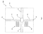
- FIG. 2 is a structure drawing for explaining an example of the embodiment of the distributed constant circuit of the present invention.
- reference numeral 10 denotes a substrate
- reference numerals 11, 12 denote a micro strip line provided on the top face of the substrate
- reference numeral 15 denotes an input terminal to the micro strip line
- reference numeral 16 denotes an output terminal from the micro strip line
- reference numeral 17 denotes a ground
- reference numeral 21 denotes a semiconductor device as an electronic device
- reference numerals 31, 32 denote a flat adjustment tab composed of conductor
- reference numeral 100 denotes a distributed constant circuit.
- the micro strip line is constituted of a ground formed on a single face of the substrate composed of dielectric material and a conductor line as a distributed constant line formed on the other side.
- the characteristic impedance of the micro strip line is determined depending on the thickness of the conductor line, the length in the minor axis of the conductor line, the thickness of the substrate, and dielectric constant of a dielectric material constituting the substrate. These constants which determine the characteristic impedance become different values from their design values if manufacturing deviation is added to these values. Further, the characteristic impedance of the micro strip line fluctuates if the distributed constant circuit is stored into a case or a connector for input or output is attached.
- the load impedance and drive impedance of an electronic circuit can be different from a design value due to manufacturing deviation.
- the frequency characteristic is generated depending on floating capacitance or floating inductance so that a design load impedance or drive impedance cannot be achieved depending on which frequency band to be applied.
- the adjustment tab 31 is brought into a contact with the micro strip line 11.
- the micro strip line 11 and the adjustment tab 31 are fixed. It is desirable to use solder or conductive adhesive agent for this fixing. As a consequence, electric connection between the micro strip line 11 and the adjustment tab 31 can be carried out securely thereby preventing the adjustment tab from moving carelessly.
- the adjustment tab 31 is moved.
- the moving direction is in the major axis or minor axis of the micro strip line 11. This may be oblique to the major axis of the micro strip line 11 by summing up the moves in the major direction and minor direction.
- the adjustment tab 31 may be moved in a condition in contact with the micro strip line 11. If it is moved in the condition in contact with the micro strip line 11, whether or not impedance matching is achieved during that moving can be evaluated. It is convenient to use a pair of tweezers for holding a tip of the dielectric material upon moving.
- the adjustment tab 31 is separated from the micro strip line 11 and by moving the adjustment tab 31 again, it is brought into a contact with the micro strip line 11. If solder is used for fixing the micro strip line 11 and the adjustment tab 31, the adjustment tab 31 can be separated from the micro strip line 11 by heating solder.
- impedance matching between the characteristic impedance of the micro strip line 12 and the drive impedance of the semiconductor device 21 can be carried out in the same operation. This impedance matching can be adjusted by moving the adjustment tab 32 into a contact with the micro strip line 12.
- the semiconductor device 21 is exemplified in FIG. 2 as the electric device, it is permissible to combine a passive device or other semiconductor device as the electronic device. Although an adjustment tab is disposed for each micro strip, it is permissible to use a plurality of the adjustment tabs. Although the ground 17 is provided on each of both sides of the semiconductor device 21, this may be provided on only one side or conductive with an opposite side through a via hole.
- W denotes the length of the minor axis of the micro strip line 11
- L denotes the length in the minor axis direction of the micro strip line 11 of a portion projecting from the micro strip line 11, that is to say, as shown in FIG. 3 , the length of the portion projecting from the micro strip line 11 of the adjustment tab 31 from the side end of the micro strip line 11 up to the front end of the adjustment tab 31 (hereinafter this length is abbreviated as "length of the projecting portion of the adjustment tab").
- the shape of the adjustment tab is a rounded corner square in FIG. 3
- the present invention is not restricted to this shape. This may be circular, elliptic, rectangular or polygon or the like.
- L ⁇ W Because the micro strip line is designed for TEM mode propagation, usually, the length W of the minor axis of the micro strip line is set to equal to or less than 1/8 a wavelength of the frequency to be propagated. If the sum of the length W of the minor axis of the micro strip line and the length L of a projecting portion of the adjustment tab is 1/4 the wavelength of the frequency of a signal to be propagated by bringing the adjustment tab into contact with the micro strip line, a standing wave can be generated in the direction of the minor axis of the micro strip line and at a portion of the adjustment tab. If the standing wave is generated, resonance occurs so that the propagation characteristic is damped largely, the phase is shifted or the characteristic impedance fluctuates largely. Thus, it is preferable that L ⁇ W.
- a portion projecting from the micro strip line 11 of the adjustment tab 31 is preferred to be chamfered.
- the adjustment tab is chamfered so as to have no sharp angle. Although it may be chamfered linearly or circularly, the present invention is not restricted to these shapes.
- FIG. 4 is a structure drawing for explaining an example of other embodiment of the distributed constant circuit of the present invention.
- reference numeral 10 denotes a substrate composed of dielectric material
- reference numerals 13, 14 denote a coplanar line provided on the top face of the substrate 10 as a conductor line
- reference numeral 15 denotes an input terminal to the coplanar line
- reference numeral 16 denotes an output terminal from the coplanar line
- reference numeral 18 denotes a ground face
- reference numeral 21 denotes a semiconductor device as an electronic device
- reference numerals 31, 32 denote a flat adjustment tab composed of conductor
- reference numeral 200 denotes a distributed constant circuit.
- the coplanar line is constituted of conductor lines formed on one face of the substrate from dielectric material and ground faces formed on both sides of conductor lines.
- the characteristic impedance of the coplanar line is determined depending on the thickness of the conductor line, the length in the minor axis of the conductor line, the gap between the conductor line and ground, the thickness of the substrate and the dielectric constant of the dielectric material constituting the substrate. If manufacturing deviation is added to these constants which determine the characteristic impedance, they become different values from their design values. Further, if the distributed constant circuit is accommodated in a case or a connector for input/output is attached, the characteristic impedance of the coplanar line fluctuates.
- the load impedance and drive impedance of an electronic circuit can be different from their design values because of manufacturing deviation. Further, the frequency characteristic is generated depending on floating capacitance or floating inductance so that a design load impedance or drive impedance cannot be achieved depending on which frequency band to be applied.
- the adjustment tab 31 is brought into a contact with the coplanar line 13.
- the coplanar line 13 and the adjustment tab 31 are fixed. It is preferable to use solder or conductive adhesive agent for the fixing. As a result, the coplanar line 13 and the adjustment tab 31 can be connected electrically securely and additionally the adjustment tab can be prevented from being moved carelessly.
- the method of adjusting the impedance adjustment using the adjustment tab 31 is the same as the case of the micro strip line.
- the impedance matching between the characteristic impedance of the coplanar line 14 and the drive impedance of the electronic device 21 using the adjustment tab 32 is the same as in the case of the micro strip line. Because in the case of the coplanar line, the ground face is close to the coplanar line, the impedance matching is changed largely only by a slight adjustment as compared with the case of the micro strip line.
- the adjustment tab of the present invention can be disposed in a small area so that the impedance matching can be adjusted easily.
- the length of the projecting portion of the adjusting tab and the shape of the projecting portion of the adjustment tab are the same as described in FIG. 3 .
- the distributed constant circuit of the embodiment of the present invention can achieve the impedance matching between the electronic device and the conductor line by bringing the adjustment tab composed of a movable conductor into a contact with the conductor line.
- the impedance matching can be adjusted easily even if an electronic device is disposed in a small area and if the adjustment of the impedance matching is unnecessary, the characteristic of the conductor line can be provided only by removing the adjustment tab. Further, by fixing the adjustment tab to the conductor line, the impedance matching can be secured stably.
- FIG. 5 shows an example of the distributed constant circuit in which the pattern produced by overlapping the adjustment tab described previously in FIG. 5 on the conductor line is uses as a new conductor line pattern.
- Reference numerals 33, 34 denote a projecting portion and reference numeral 300 denotes a distributed constant circuit.
- the projecting portions 33, 34 are chamfered, concentration of electric field can be prevented and even if the distributed constant circuit 100 is installed in a case or the like, an influence upon the distribution of electric field is small. Because the length of a portion of the projecting portion 33, 34, which projects from the micro strip line 11 or 12 in the direction of the minor axis of the micro strip line 11 or 12, is equal to or shorter than the length in the direction of the minor axis of the micro strip line 11 or 12, generation of standing wave in the direction of the minor axis of the micro strip line 11 or 12 can be prevented.
- the same effect can be obtained.
- the distributed constant circuit having such a coplanar line can secure the impedance matching between the characteristic impedance of the coplanar line and the load impedance or drive impedance of an electronic device after it is manufactured.
- the distributed constant circuit and impedance adjustment method of the present invention can be applied for a radio device using high frequency, an amplifier of coaxial CATV using carrier wave and adjustment thereof.
Landscapes
- Waveguides (AREA)
Claims (2)
- Schaltung (100, 200) mit verteilten Konstanten, miteinem Substrat (10) aus einem Dielektrikum,einer auf einer Oberseite des Substrats (10) vorgesehenen Leiterbahn (11, 12),einem an die Leiterbahn (11, 12) angeschlossenen elektronischen Bauelement (21) undeinem Einstellstreifen (31, 32), der aus einem Flachleiter besteht, der mit der Leiterbahn (11, 12) in Kontakt steht,dadurch gekennzeichnet, daß ein Teil des Einstellstreifens (31, 32), der von der Leiterbahn (11, 12) vorsteht, abgerundet ist und ein Abschnitt (L) des vorstehenden Teils des Einstellstreifens (31, 32) kleiner oder gleich einer Länge (W) einer kleinen Achse der Leiterbahn (11, 12) ist.
- Schaltung (300) mit verteilten Konstanten, miteinem Substrat (10) aus einem Dielektrikum,einer auf einer Oberseite des Substrats (10) vorgesehenen Leiterbahn (11, 12) mit einem vorstehenden Teil (33, 34) auf der Substratoberfläche undeinem an die Leiterbahn (11, 12) angeschlossenen elektronischen Bauelement (21),dadurch gekennzeichnet, daß der vorstehende Teil (33, 34) abgerundet ist und ein Abschnitt des vorstehenden Teils (33, 34) kleiner oder gleich einer Länge einer kleinen Achse der Leiterbahn (11, 12) ist.
Applications Claiming Priority (1)
| Application Number | Priority Date | Filing Date | Title |
|---|---|---|---|
| JP2005104685A JP2006287619A (ja) | 2005-03-31 | 2005-03-31 | 分布定数回路及びインピーダンス調整方法 |
Publications (2)
| Publication Number | Publication Date |
|---|---|
| EP1708302A1 EP1708302A1 (de) | 2006-10-04 |
| EP1708302B1 true EP1708302B1 (de) | 2008-06-11 |
Family
ID=36278749
Family Applications (1)
| Application Number | Title | Priority Date | Filing Date |
|---|---|---|---|
| EP06005190A Expired - Fee Related EP1708302B1 (de) | 2005-03-31 | 2006-03-14 | Schaltung mit verteilten Parametern und Verfahren zur Impedanzanpassung |
Country Status (4)
| Country | Link |
|---|---|
| US (1) | US20060220761A1 (de) |
| EP (1) | EP1708302B1 (de) |
| JP (1) | JP2006287619A (de) |
| DE (1) | DE602006001416D1 (de) |
Families Citing this family (1)
| Publication number | Priority date | Publication date | Assignee | Title |
|---|---|---|---|---|
| JP2011101327A (ja) * | 2009-11-09 | 2011-05-19 | Canon Inc | 信号伝送路 |
Family Cites Families (7)
| Publication number | Priority date | Publication date | Assignee | Title |
|---|---|---|---|---|
| JPS5894201A (ja) * | 1981-11-28 | 1983-06-04 | Mitsubishi Electric Corp | ストリツプ線路における調整装置 |
| US4701727A (en) * | 1984-11-28 | 1987-10-20 | General Dynamics, Pomona Division | Stripline tapped-line hairpin filter |
| US5164688A (en) * | 1991-05-31 | 1992-11-17 | Hughes Aircraft Company | Miniature microwave and millimeter wave tuner |
| JP2812291B2 (ja) | 1996-03-15 | 1998-10-22 | 日本電気株式会社 | 高周波トランジスタ整合回路 |
| JPH1138372A (ja) * | 1997-07-24 | 1999-02-12 | Oki Electric Ind Co Ltd | 高周波回路、それを用いた光モジュール及びインピーダンス整合方法 |
| JP2001144510A (ja) * | 1999-11-15 | 2001-05-25 | Nec Corp | マイクロ波回路の特性調整回路および特性調整方法 |
| US6504448B1 (en) * | 2000-08-08 | 2003-01-07 | Rambus Inc. | Apparatus and method for transmission line impedance tuning using periodic capacitive stubs |
-
2005
- 2005-03-31 JP JP2005104685A patent/JP2006287619A/ja active Pending
-
2006
- 2006-03-13 US US11/373,095 patent/US20060220761A1/en not_active Abandoned
- 2006-03-14 EP EP06005190A patent/EP1708302B1/de not_active Expired - Fee Related
- 2006-03-14 DE DE602006001416T patent/DE602006001416D1/de not_active Expired - Fee Related
Also Published As
| Publication number | Publication date |
|---|---|
| DE602006001416D1 (de) | 2008-07-24 |
| EP1708302A1 (de) | 2006-10-04 |
| JP2006287619A (ja) | 2006-10-19 |
| US20060220761A1 (en) | 2006-10-05 |
Similar Documents
| Publication | Publication Date | Title |
|---|---|---|
| US6566986B2 (en) | Dielectric filter | |
| US7583168B2 (en) | Resonator | |
| US6646522B1 (en) | Voltage tunable coplanar waveguide phase shifters | |
| US9166300B2 (en) | Slot antenna | |
| US6580335B1 (en) | Waveguide-transmission line transition having a slit and a matching element | |
| US20050275489A1 (en) | Dielectric ceramic filter with metal guide-can | |
| US11569556B2 (en) | Phase shifter comprising DGS and radio communication module comprising same | |
| US7183882B2 (en) | Microstrip band pass filter using end-coupled SIRs | |
| US10128557B2 (en) | Chip-to-chip interface comprising a microstrip circuit to waveguide transition having an emitting patch | |
| JP3965762B2 (ja) | トリプレート線路層間接続器 | |
| US6819198B2 (en) | Nonreciprocal circuit device and high-frequency circuit apparatus | |
| JP2000244212A (ja) | 導波管・伝送線路変換器 | |
| US6201456B1 (en) | Dielectric filter, dielectric duplexer, and communication device, with non-electrode coupling parts | |
| JPH06303010A (ja) | 高周波伝送線路及び該高周波伝送線路を用いた集積回路装置並びに高周波平面回路の接続方法 | |
| JP2004112668A (ja) | 共振器及びフィルタ | |
| EP1708302B1 (de) | Schaltung mit verteilten Parametern und Verfahren zur Impedanzanpassung | |
| JPH10242717A (ja) | 平面誘電体集積回路 | |
| US7403085B2 (en) | RF module | |
| KR100539493B1 (ko) | 비방사 유전체 도파로를 이용한 방향성 결합기 | |
| US5173666A (en) | Microstrip-to-inverted-microstrip transition | |
| JP4105017B2 (ja) | 導波管型誘電体フィルタ | |
| US6982608B2 (en) | Isolator suitable for miniaturization | |
| EP0869573B1 (de) | Dielektrisches Filter und Kommunikationsgerät damit | |
| KR20070075936A (ko) | Sir형 밴드패스필터 | |
| JP3398527B2 (ja) | 伝送線路の交差構造 |
Legal Events
| Date | Code | Title | Description |
|---|---|---|---|
| PUAI | Public reference made under article 153(3) epc to a published international application that has entered the european phase |
Free format text: ORIGINAL CODE: 0009012 |
|
| AK | Designated contracting states |
Kind code of ref document: A1 Designated state(s): AT BE BG CH CY CZ DE DK EE ES FI FR GB GR HU IE IS IT LI LT LU LV MC NL PL PT RO SE SI SK TR |
|
| AX | Request for extension of the european patent |
Extension state: AL BA HR MK YU |
|
| 17P | Request for examination filed |
Effective date: 20070306 |
|
| 17Q | First examination report despatched |
Effective date: 20070416 |
|
| AKX | Designation fees paid |
Designated state(s): DE FR GB IT SE |
|
| GRAP | Despatch of communication of intention to grant a patent |
Free format text: ORIGINAL CODE: EPIDOSNIGR1 |
|
| GRAS | Grant fee paid |
Free format text: ORIGINAL CODE: EPIDOSNIGR3 |
|
| GRAA | (expected) grant |
Free format text: ORIGINAL CODE: 0009210 |
|
| AK | Designated contracting states |
Kind code of ref document: B1 Designated state(s): DE FR GB IT SE |
|
| REG | Reference to a national code |
Ref country code: GB Ref legal event code: FG4D |
|
| REF | Corresponds to: |
Ref document number: 602006001416 Country of ref document: DE Date of ref document: 20080724 Kind code of ref document: P |
|
| REG | Reference to a national code |
Ref country code: SE Ref legal event code: TRGR |
|
| PLBE | No opposition filed within time limit |
Free format text: ORIGINAL CODE: 0009261 |
|
| STAA | Information on the status of an ep patent application or granted ep patent |
Free format text: STATUS: NO OPPOSITION FILED WITHIN TIME LIMIT |
|
| 26N | No opposition filed |
Effective date: 20090312 |
|
| PG25 | Lapsed in a contracting state [announced via postgrant information from national office to epo] |
Ref country code: IT Free format text: LAPSE BECAUSE OF FAILURE TO SUBMIT A TRANSLATION OF THE DESCRIPTION OR TO PAY THE FEE WITHIN THE PRESCRIBED TIME-LIMIT Effective date: 20080611 |
|
| PGFP | Annual fee paid to national office [announced via postgrant information from national office to epo] |
Ref country code: DE Payment date: 20090323 Year of fee payment: 4 Ref country code: SE Payment date: 20090312 Year of fee payment: 4 |
|
| PGFP | Annual fee paid to national office [announced via postgrant information from national office to epo] |
Ref country code: FR Payment date: 20090312 Year of fee payment: 4 |
|
| EUG | Se: european patent has lapsed | ||
| GBPC | Gb: european patent ceased through non-payment of renewal fee |
Effective date: 20100314 |
|
| REG | Reference to a national code |
Ref country code: FR Ref legal event code: ST Effective date: 20101130 |
|
| PG25 | Lapsed in a contracting state [announced via postgrant information from national office to epo] |
Ref country code: FR Free format text: LAPSE BECAUSE OF NON-PAYMENT OF DUE FEES Effective date: 20100331 |
|
| PG25 | Lapsed in a contracting state [announced via postgrant information from national office to epo] |
Ref country code: DE Free format text: LAPSE BECAUSE OF NON-PAYMENT OF DUE FEES Effective date: 20101001 |
|
| PG25 | Lapsed in a contracting state [announced via postgrant information from national office to epo] |
Ref country code: GB Free format text: LAPSE BECAUSE OF NON-PAYMENT OF DUE FEES Effective date: 20100314 |
|
| PG25 | Lapsed in a contracting state [announced via postgrant information from national office to epo] |
Ref country code: SE Free format text: LAPSE BECAUSE OF NON-PAYMENT OF DUE FEES Effective date: 20100315 |