EP1708209A1 - Chip inductor and process for producing the same - Google Patents
Chip inductor and process for producing the same Download PDFInfo
- Publication number
- EP1708209A1 EP1708209A1 EP04821197A EP04821197A EP1708209A1 EP 1708209 A1 EP1708209 A1 EP 1708209A1 EP 04821197 A EP04821197 A EP 04821197A EP 04821197 A EP04821197 A EP 04821197A EP 1708209 A1 EP1708209 A1 EP 1708209A1
- Authority
- EP
- European Patent Office
- Prior art keywords
- turns
- conductor patterns
- plural
- conductor pattern
- chip inductor
- Prior art date
- Legal status (The legal status is an assumption and is not a legal conclusion. Google has not performed a legal analysis and makes no representation as to the accuracy of the status listed.)
- Withdrawn
Links
Images



Classifications
-
- H—ELECTRICITY
- H01—ELECTRIC ELEMENTS
- H01F—MAGNETS; INDUCTANCES; TRANSFORMERS; SELECTION OF MATERIALS FOR THEIR MAGNETIC PROPERTIES
- H01F17/00—Fixed inductances of the signal type
-
- H—ELECTRICITY
- H01—ELECTRIC ELEMENTS
- H01F—MAGNETS; INDUCTANCES; TRANSFORMERS; SELECTION OF MATERIALS FOR THEIR MAGNETIC PROPERTIES
- H01F17/00—Fixed inductances of the signal type
- H01F17/0006—Printed inductances
- H01F17/0013—Printed inductances with stacked layers
-
- H—ELECTRICITY
- H01—ELECTRIC ELEMENTS
- H01F—MAGNETS; INDUCTANCES; TRANSFORMERS; SELECTION OF MATERIALS FOR THEIR MAGNETIC PROPERTIES
- H01F41/00—Apparatus or processes specially adapted for manufacturing or assembling magnets, inductances or transformers; Apparatus or processes specially adapted for manufacturing materials characterised by their magnetic properties
- H01F41/02—Apparatus or processes specially adapted for manufacturing or assembling magnets, inductances or transformers; Apparatus or processes specially adapted for manufacturing materials characterised by their magnetic properties for manufacturing cores, coils, or magnets
- H01F41/04—Apparatus or processes specially adapted for manufacturing or assembling magnets, inductances or transformers; Apparatus or processes specially adapted for manufacturing materials characterised by their magnetic properties for manufacturing cores, coils, or magnets for manufacturing coils
- H01F41/041—Printed circuit coils
-
- H—ELECTRICITY
- H01—ELECTRIC ELEMENTS
- H01F—MAGNETS; INDUCTANCES; TRANSFORMERS; SELECTION OF MATERIALS FOR THEIR MAGNETIC PROPERTIES
- H01F41/00—Apparatus or processes specially adapted for manufacturing or assembling magnets, inductances or transformers; Apparatus or processes specially adapted for manufacturing materials characterised by their magnetic properties
- H01F41/02—Apparatus or processes specially adapted for manufacturing or assembling magnets, inductances or transformers; Apparatus or processes specially adapted for manufacturing materials characterised by their magnetic properties for manufacturing cores, coils, or magnets
- H01F41/04—Apparatus or processes specially adapted for manufacturing or assembling magnets, inductances or transformers; Apparatus or processes specially adapted for manufacturing materials characterised by their magnetic properties for manufacturing cores, coils, or magnets for manufacturing coils
- H01F41/06—Coil winding
-
- H—ELECTRICITY
- H01—ELECTRIC ELEMENTS
- H01F—MAGNETS; INDUCTANCES; TRANSFORMERS; SELECTION OF MATERIALS FOR THEIR MAGNETIC PROPERTIES
- H01F17/00—Fixed inductances of the signal type
- H01F17/0006—Printed inductances
- H01F17/0013—Printed inductances with stacked layers
- H01F2017/002—Details of via holes for interconnecting the layers
Definitions
- the present invention relates to a chip inductor including alternately laminated conductor patterns constituting a coil and insulating layers, as well as a method for manufacturing the same.
- a chip inductor is formed into the shape of a small, low-profile chip in outline, and is one type of extremely high performance, versatile electronic component compatible with miniaturization and slimming of electronic equipment.
- the chip inductor is incorporated into various electronic circuits, and is used as a noise filter, for example.
- Patent Document 1 A first example of known technologies related to this type of inductor is a technology disclosed in Patent Document 1, for example.
- This inductor is a laminated inductor constructed by alternately laminating coil conductors and low dielectric constant insulating films on an insulating substrate, and connecting the coil conductors located on and under the individual low dielectric constant insulating film to each other through a window portion provided in the low dielectric constant insulating film (so-called interlayer connection), so as to form one series of coil connected in series in the entire chip inductor.
- laminated inductor laminates of the coil conductors and the low dielectric constant insulating films are further layered to increase the inductance of the above-described one series of coil as a whole.
- a second known technology is a technology disclosed in Patent Document 2, for example.
- coil conductors having the large numbers of turns are disposed on an upper layer side and a lower layer side of the laminate in the above-described laminated inductor, and coil conductors having the small numbers of turns are disposed as intermediate layers sandwiched between the upper layer and the lower layer, so that the distribution of the direct-current resistance value is made non-uniform all over the coil. That is, the middle portion (intermediate layer portion) of the laminate is made to have low direct-current resistance, and the portions nearer to the outside, such as the upper layer and the lower layer, are made to have high direct-current resistance. In this manner, it is attempted to reduce the pressure bonding strain during production of the laminate, as well as to improve the heat dissipation characteristics of the laminated inductor.
- Patent Document 1 Japanese Unexamined Patent Application Publication No. 9-17634
- Patent Document 2 Japanese Unexamined Patent Application Publication No. 2002-246231
- the laminates of the coil conductors and the low dielectric constant insulating layers are further layered to increase the inductance of the entire coil, although the line width may not be reduced, the thickness (height) of the external dimension of the entire laminate is increased by the thickness of the further layered portion. Therefore, advantages of the chip inductor, i.e. small size and low profile, may be impaired.
- the coil conductors having the large numbers of turns are disposed on the upper layer side and the lower layer side of the laminate, excellent heat dissipation characteristics can be attained while the inductance is increased.
- the line width of the coil conductor must be increased in order to reduce the direct-current resistance value. Consequently, the inner diameter of the coil is decreased correspondingly, the inductance is decreased, and the Q characteristic may be reduced.
- setting of the line width is restricted. Therefore, when this layer is fired during the manufacturing of a chip inductor, the line width of this layer is decreased by shrinkage and, as a result, there is also a problem in that the direct-current resistance value is increased.
- the present invention was made to overcome the above-described problems. Accordingly, it is an object of the present invention to provide a chip inductor in which excellent Q characteristic is realized while advantages in its small size and low profile are ensured, as well as a method for manufacturing the same.
- an invention according to Claim 1 is a chip inductor provided with a chip main body and a pair of external connection electrodes, the chip main body composed of a substrate and a laminate including plural conductor patterns and plural insulating layers alternately laminated on the substrate while the plural conductor patterns are connected to each other in series in the lamination direction thereof so as to constitute a coil, one of the external connection electrodes attached to one side-end face of the chip main body and connected to one end of the coil, and the other external connection electrode attached to the other side-end face and connected to the other end of the coil, wherein the outer diameter dimensions of the plural conductor patterns constituting the coil are specified to be substantially equal and any one of plural conductor patterns in the lower half of the plural conductor patterns is specified to be a conductor pattern having the largest number of turns, and the thickness of the laminate and the thickness of the substrate are specified to be substantially equal, so that the lowermost-layer conductor pattern is located substantially in the midsection of the chip main body.
- any one of the plural conductor patterns located in the lower half of the plural conductor patterns becomes the conductor pattern having the largest number of turns and, therefore, the inductance is increased correspondingly. Since the plural conductor patterns other than the above-described conductor pattern have small numbers of turns, the direct-current resistance of the entire coil can be maintained at a low value.
- An invention according to Claim 2 is the chip inductor described in Claim 1, wherein the lowermost-layer conductor pattern is specified to be the conductor pattern having the largest number of turns and, in addition, the numbers of turns of the other plural conductor patterns are specified to be substantially equal to each other.
- An invention according to Claim 3 is the chip inductor described in Claim 2, wherein the number of turns of the lowermost-layer conductor pattern is specified to be about 1.5 times the numbers of turns of the other plural conductor patterns.
- the inductance value of the entire coil can be further improved and, in addition, an increase in the direct-current resistance value can be further suppressed.
- An invention according to Claim 4 is the chip inductor described in Claim 3, wherein the number of turns of the lowermost-layer conductor pattern is specified to be about 1.5 turns, and the numbers of turns of the other conductor patterns are specified to be about 1 turn.
- An invention according to Claim 5 is the chip inductor described in any one of Claim 1 to Claim 4, wherein each of the external connection electrodes has a sectional shape similar to that of a square bracket extending from a top surface of the chip main body to a bottom surface along the side-end face.
- An invention according to Claim 6 is the chip inductor described in Claim 5, wherein each of the external connection electrodes is disposed so as to prevent the magnetic fluxes generated by the coil from passing through portions of the external connection electrodes located on the top surface and the bottom surface of the chip main body.
- the external connection electrodes do not interrupt the magnetic field generated by the coil in this chip inductor.
- An invention according to Claim 7 is the chip inductor described in any one of Claim 1 to Claim 6, wherein the plural conductor patterns are connected in series in the lamination direction through openings disposed in the insulating layers so as to constitute the coil.
- An invention according to Claim 8 is the chip inductor described in any one of Claim 1 to Claim 7, wherein the substrate is a ceramic substrate or a wafer, the conductor patterns are disposed by patterning and firing a photosensitive conductor paste, and the insulating layers are disposed by firing an insulating material paste.
- An invention according to Claim 9 is the chip inductor described in any one of Claim 1 to Claim 8, wherein the line widths of the plural conductor patterns are specified to be substantially equal to each other.
- An invention according to Claim 10 is a method for manufacturing a chip inductor, wherein a step of forming a conductor pattern by patterning and firing a photosensitive conductor paste and a following step of firing an insulating layer are alternately repeated plural times on a ceramic substrate or a wafer so as to produce a chip inductor including a coil constructed by connecting the plural conductor patterns to each other in series in the lamination direction, the method including the step of setting the number of turns of the lowermost-layer conductor pattern, among the plural conductor patterns, disposed immediately above the ceramic substrate or the wafer to be larger than the numbers of turns of the other plural conductor patterns, and setting the numbers of turns of the other plural conductor patterns to be substantially equal to each other.
- the shrinkage during the firing is less than those of the other plural conductor patterns disposed on the insulating layers.
- the number of turns can be made larger than the numbers of turns of the other plural conductor patterns, while a desired line width is ensured.
- An invention according to Claim 11 is the method for manufacturing a chip inductor described in Claim 10, wherein the lowermost-layer conductor pattern is formed to have the number of turns of about 1.5 times the numbers of turns of the other plural conductor patterns.
- An invention according to Claim 12 is the method for manufacturing a chip inductor described in Claim 10 or Claim 11, wherein openings are disposed in the insulating layers, and the plural conductor patterns are connected to each other in series in the lamination direction thereof through the openings so as to constitute the coil.
- the inductance of the coil in which plural conductor patterns are connected in series can be increased and, in addition, the direct-current resistance of the coil can be maintained at a low value. Consequently, the Q characteristic of the entire coil can be improved.
- the chip inductor related to the invention described in Claim 2 in the coil, only the lowermost-layer conductor pattern has the largest number of turns and, therefore, the inductance is increased correspondingly. Since the plural conductor patterns, which hold the great majority, other than the lowermost-layer conductor pattern, are in no need of having large numbers of turns, the direct-current resistance of the entire coil can be maintained at a low value. As a result, the Q characteristic of the entire coil can be improved. Since only the lowermost-layer conductor pattern is made to have the largest number of turns and, thereby, the inductance is increased, as described above, slimming of the entire inductor can be achieved without increasing the number of lamination of the conductor patterns.
- the chip inductor related to the invention described in Claim 3 since the number of turns of the lowermost-layer conductor pattern is specified to be about 1.5 times the numbers of turns of the other plural conductor patterns, an increase in the inductance value and suppression of increase in the direct-current resistance value of the entire coil can be achieved. Consequently, the Q characteristic of the entire coil can be further improved.
- the chip inductor related to the invention described in Claim 6 since the external connection electrodes do not interrupt the magnetic field generated by the coil, the inductance of the entire coil can be further improved, and further improvement of the Q characteristic can be achieved.
- the inductance can be increased by increasing the number of turns of the lowermost-layer conductor pattern without increasing the number of lamination of the layers, and the line width can be ensured by decreasing the numbers of turns of the plural conductor patterns other than the lowermost-layer conductor pattern. Furthermore, since the shrinkage of the lowermost-layer conductor pattern during the firing is less than those of the other plural conductor patterns disposed on the insulating layers and a desired line width is substantially maintained, the direct-current resistance value of the entire coil can be lowered. As a result, the Q characteristic of the entire coil can be improved while the entire inductor remains low-profile.
- Fig. 1 is an perspective exploded view of a chip inductor according to an example of the present invention
- Fig. 2 is a perspective view showing an appearance thereof
- Fig. 3 is a sectional view of a section showing via hole portions, the section taken along a line A-A shown in Fig. 2.
- Fig. 4 is a sectional view of a section showing junctions between a coil and external connection electrodes disposed in the chip inductor, the section taken along a line B-B shown in Fig. 2.
- a chip inductor 1 of the present Example is composed of a ceramic substrate 2, a laminate 3 disposed thereon by lamination, and external connection electrodes 4-1 and 4-2 attached to the left end and the right end, respectively, of a chip main body including the ceramic substrate 2 and the laminate 3.
- the ceramic substrate 2 is produced by cutting a substrate of 0.15 [mm] in thickness formed through firing of an alumina material into a very small size of about 0.6 [mm] in length by 0.3 [mm] in width.
- the laminate 3 is produced by alternately laminating plural conductor patterns 31 to 34 having the same outer diameter dimension R and plural insulating layers 35 to 38.
- the conductor pattern 31 among the plural conductor patterns 31 to 34 is a conductor pattern having the largest number of turns, and is disposed immediately on the surface of the ceramic substrate 2, so as to be located as the lowermost layer.
- the number of turns of this conductor pattern 31 is about 1.5 turns, and is specified to be about 1.5 times the numbers of turns of the other plural conductor patterns 32, 33, and 34. Therefore, each of the numbers of turns of the other plural conductor patterns 32, 33, and 34 is specified to be about 1 turn.
- the line width of the thus configured conductor patterns 31 to 34 are specified to be substantially equal, and the conductor patterns 31 to 34 are sequentially connected in series in the lamination direction thereof through their respective openings, i.e. via holes 51, 52, and 53, so as to constitute a coil 30.
- the conductor pattern 31 having the number of turns of 1.5 turns is disposed on the ceramic substrate 2, and the insulating layer 35 is disposed by lamination while covering this conductor pattern 31 and the surface of the ceramic substrate 2.
- the conductor pattern 32 having the number of turns of about 1 turn is disposed on the surface of the insulating layer 35, and the insulating layer 36 is disposed by lamination while covering this conductor pattern 32 and the surface of the insulating layer 35.
- the conductor pattern 33 having the number of turns of about 1 turn is disposed on the surface of the insulating layer 36, and the insulating layer 37 is disposed by lamination while covering this conductor pattern 33 and the surface of the insulating layer 36.
- the conductor pattern 34 having the number of turns of about 1 turn is disposed on the surface of this insulating layer 37, and the insulating layer 38 doubling as an exterior layer is disposed by lamination while covering this conductor pattern 34 and the surface of the insulating layer 37.
- the conductor patterns 31 to 34 constituting respective sections of the laminate 3, as described above, are produced by patterning and firing a photosensitive paste primarily containing silver, glass, and the like, as described below, and the insulating layers 35 to 38 are produced by printing and firing an insulating paste primarily containing glass and the like.
- the thickness of this laminate 3 is equal to the thickness of the ceramic substrate 2 and is about 0.15 [mm]. That is, the thickness of the ceramic substrate 2 is specified to be about one-half the thickness of the entire chip inductor. Therefore, the lowermost-layer conductor pattern 31 disposed immediately on the surface of the ceramic substrate 2 is located substantially in the midsection in the thickness direction of the chip main body composed of the ceramic substrate 2 and the laminate 3.
- each of the external connection electrodes 4-1 and 4-2 is in the shape similar to that of a square bracket, and are attached to their respective side-end faces of the chip main body composed of the ceramic substrate 2 and the laminate 3 while covering a part of the top surface and a part of the bottom surface, as well as their respective side-end faces. That is, as shown in Fig. 3, each of the external connection electrodes 4-1 and 4-2 has a cross-section in the shape of a square bracket extending from a top surface of the insulating layer 38, which is the top surface of the chip main body, to a bottom surface of the ceramic substrate 2, which is the bottom surface of the chip main body, along the side-end face (a left or right side-face in Fig. 3) of the chip main body.
- These external connection electrodes 4-1 and 4-2 are connected to respective terminals of the coil 30. Specifically, as shown in Fig. 4, the external connection electrode 4-1 is connected to the conductor pattern 31, and the external connection electrode 4-2 is connected to the conductor pattern 34. Each of the surfaces of these external connection electrodes 4-1 and 4-2 is plated with Ni, Sn, Cu, or the like, and therefore, excellent electrical conductivity, excellent connectivity to the outside, and the like are exhibited.
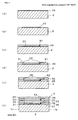
- Fig. 5 is a step diagram showing a main flow of a production process of this chip inductor.
- a photosensitive conductor paste 39 is applied to the surface of the ceramic substrate 2.
- the resulting paste is patterned by photolithography to prepare an unfired pattern in the shape of a partial sheet coil of about 1.5 turns, and firing is performed, so that the lowermost-layer conductor pattern 31 of about 1.5 turns is formed, as shown in Fig. 5(b).
- the unfired conductor pattern tends to shrink during firing.
- shrinkage of the line width of the conduction portion 31 during the firing is very little as compared with shrinkage of the line widths of the other conductor patterns 32, 33, and 34.
- the insulating layer 35 is formed to cover the conductor pattern 31 and the surface of the ceramic substrate 2, a via hole 51 is formed and, thereafter, firing is performed.
- a photosensitive conductor paste 39 similar to that described above is applied to the surface of the insulating layer 35 (not shown in the drawing).
- the resulting paste is patterned by photolithography to form an unfired pattern in the shape of a partial sheet coil of about 1 turn.
- the photosensitive conductor paste 39 enters the via hole 51.
- the pattern is fired in such a state and, thereby, the conductor pattern 32 having the number of turns of about 1 turn is formed.
- This conductor pattern 32 is brought into the state of being electrically connected to the conductor pattern 31 through the via hole 51.
- the insulating layer 35 contains glass as a primary material and the unfired conductor pattern disposed thereon is made of a silver paste material, the glass serves as a promoter of sintering of silver, and the shrinkage of the line width of the conductor pattern 32 is increased. Consequently, the conductor pattern 32 produced by the firing shrinks significantly as compared with that in the case where the conductor pattern 31 is fired.
- this conductor pattern 32 is specified to have the number of turns smaller than that of the lowermost-layer conductor pattern 31, it is possible to take the decrement of the line width due to the above-described shrinkage into consideration in advance and to set the dimensions of the line width and the like of the unfired conductor pattern 32 at the large side correspondingly.
- the conductor pattern 32 can also be formed to have a desired line width. More preferably, the line width of the conductor pattern 32 is set to become substantially equal to the line width of the conductor pattern 31.
- the insulating layer 36 is formed to cover the conductor pattern 32 and the surface of the insulating layer 35, a via hole 52 is formed and, thereafter, firing is performed.
- the conductor pattern 33 having the same number of turns as that of the conductor pattern 32, the insulating layer 37 including a via hole 53 as in the insulating layer 35, the conductor pattern 34 having the same number of turns as that of the conductor pattern 32, and the insulating layer 38 doubling as a protective layer are sequentially formed in that order by lamination on this insulating layer 36.
- the thus prepared wafer is divided by scribing and roller breaking, so that each chip main body of about 0.6 [mm] by 0.3 [mm] is produced.
- the lowermost-layer conductor pattern 31 of about 1.5 turns and the other conductor patterns 32, 33, and 34 of about 1 turn are connected in series in the lamination direction thereof through via holes 51, 52, and 53, so as to constitute the coil 30.
- the external connection terminals 4-1 and 4-2 in the state of being connected to the two respective ends of this coil 30 are attached to the two side-ends 1a and 1b, respectively, of the chip main body by baking, plating, or the like, so that the chip inductor 1 shown in Fig. 1 to Fig. 3 is completed.
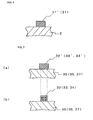
- Fig. 6 is a sectional view showing a state of the lowermost-layer conductor pattern during the firing.
- Fig. 7 is a sectional view schematically showing a shrinkage phenomenon of the other conductor patterns in a line width direction during the firing.
- the lowermost-layer conductor pattern 31 is disposed immediately on the ceramic substrate 2. Consequently, glass is not present in the ceramic substrate 2, while the glass serves as a promoter of sintering of the conductor pattern 31. Therefore, the line width of the conductor pattern 31 is hardly decreased when an entire unfired conductor pattern 31' is fired.
- the shrinkage of the conductor pattern 31 disposed immediately on the ceramic substrate 2 is very little even after being subjected to a firing step as compared with the shrinkage of the conductor patterns 32, 33, and 34 and, therefore, the cross-sectional area thereof can be maintained at a desired size after the firing. Consequently, an increase in inductance by an increase in the number of turns can be achieved while an increase in direct-current resistance value due to the line width shrinkage is suppressed. As a result, the Q characteristic of the coil 30 can be improved. Furthermore, since the number of turns is increased in the conductor pattern 31, there is no need to increase the number of lamination of the other conductor patterns 32, 33, and 34. As a result, the entire chip inductor 1 can be slimmed.
- the conductor pattern 32' (33', 34') is disposed on the insulating layer 35 (36, 37) before firing, as shown in Fig. 7(a), the glass primarily contained in the insulating layer 35 (36, 37) serves as a promoter of sintering of silver in the conductor pattern 32' (33', 34'). Consequently, as shown in Fig. 7(b), the line width of the conductor pattern 32 (33, 34) shrinks significantly during firing as compared with that in the case where the conductor pattern 31 is fired.
- the number of turns of the conductor pattern 32 (33, 34) is about 1 turn, and is set at the number of turns smaller than that of the lowermost-layer conductor pattern 31. Therefore, it is possible to set in advance the dimension of the line width of the unfired conductor pattern 32' (33', 34') at the large side as compared with the finished measurements of the line width. Consequently, the conductor pattern 32 (33, 34) having the line width substantially equal to that of the conductor pattern 31 can be formed by taking the decrement of the line width during the firing into consideration in advance and setting the line width of the unfired conductor pattern 32' (33', 34') at the large side correspondingly.
- the conductor patterns 32, 33, and 34 can be formed to have a desired line width with a small number of turns. Consequently, the direct-current resistance of the entire coil 30 can be maintained at a low value and, as a result, the Q characteristic of the entire coil 30 can be improved.
- the number of turns of the lowermost-layer conductor pattern 31 is set at about 1.5 turns
- the numbers of turns of the other plural conductor patterns 32, 33, and 34 are equally set at about 1 turn and, thereby, an increase in the inductance value and suppression of increase in the direct-current resistance value of the entire coil 30 are enhanced. Consequently, the Q characteristic of the entire coil can be further improved.
- the Q characteristic is optimized by setting the number of turns of the lowermost-layer conductor pattern 31 at about 1.5 turns and, in addition, setting the numbers of turns of the other conductor patterns 32, 33, and 34 at about 1 turn.
- Fig. 8 is a sectional view schematically showing a state of distribution of magnetic fields in the case where the conductor pattern having the largest number of turns is disposed as the lowermost layer and is located substantially in the midsection in the thickness direction of the chip inductor.
- Fig. 9 is a sectional view schematically showing a state of distribution of magnetic fields in the case where the conductor pattern having the largest number of turns is disposed in the upper portion of the chip inductor.
- the number of turns of the conductor pattern 31 is indicated as 2 turns and the numbers of turns of the other conductor patterns are indicated as 1 turn to facilitate the explanation and the understanding.
- the conductor pattern 31 having the largest number of turns and the narrowest inner diameter is disposed as the lowermost layer and is located substantially in the midsection in the thickness direction of the chip inductor 1, while the conductor patterns 32, 33, and 34 having the small numbers of turns and wide inner diameters are disposed above the conductor pattern 31.
- the Q characteristic of the chip inductor 1 can be improved by disposing the conductor pattern 31 having the largest number of turns immediately on the ceramic substrate 2 having a thickness about one-half the thickness of the entire chip inductor 1 and locating substantially in the midsection in the thickness direction of the entire chip inductor 1.
- each chip inductor 1 was specified to be about 0.6 [mm] by 0.3 [mm]. However, it is also possible that, for example, other dimensions, e.g., 1.0 [mm] by 0.5 [mm], is adopted, or the thickness of the ceramic substrate 2 is specified to be 0.2 [mm] or 0.25 [mm].
- the ceramic substrate produced by firing alumina was used as the substrate.
- the lowermost layer conductor pattern 31 was specified to have the number of turns of about 1.5 turns, and the other conductor patterns 32, 33, and 34 were specified to have the numbers of turns of about 1 turn. However, the numbers of turns are not limited to them.
- the lowermost-layer conductor pattern 31 was specified to have the largest number of turns, but not limited to this. That is, any one of the conductor patterns 31 and 32 located in the lower half portion of the plural conductor patterns 31 to 34 may be specified to have the largest number of turns.
Landscapes
- Engineering & Computer Science (AREA)
- Power Engineering (AREA)
- Microelectronics & Electronic Packaging (AREA)
- Manufacturing & Machinery (AREA)
- Coils Or Transformers For Communication (AREA)
- Manufacturing Cores, Coils, And Magnets (AREA)
Abstract
Description
- The present invention relates to a chip inductor including alternately laminated conductor patterns constituting a coil and insulating layers, as well as a method for manufacturing the same.
- A chip inductor is formed into the shape of a small, low-profile chip in outline, and is one type of extremely high performance, versatile electronic component compatible with miniaturization and slimming of electronic equipment. The chip inductor is incorporated into various electronic circuits, and is used as a noise filter, for example.
- A first example of known technologies related to this type of inductor is a technology disclosed in
Patent Document 1, for example. This inductor is a laminated inductor constructed by alternately laminating coil conductors and low dielectric constant insulating films on an insulating substrate, and connecting the coil conductors located on and under the individual low dielectric constant insulating film to each other through a window portion provided in the low dielectric constant insulating film (so-called interlayer connection), so as to form one series of coil connected in series in the entire chip inductor. In this laminated inductor, laminates of the coil conductors and the low dielectric constant insulating films are further layered to increase the inductance of the above-described one series of coil as a whole. That is, the total number of turns of the entire coil is increased and, thereby, a desired high inductance value is attained while the line width and the thickness of each coil conductor are ensured to achieve a reduction in direct-current resistance. As a result, realization of excellent Q characteristic is directed. - A second known technology is a technology disclosed in
Patent Document 2, for example. In this technology, coil conductors having the large numbers of turns are disposed on an upper layer side and a lower layer side of the laminate in the above-described laminated inductor, and coil conductors having the small numbers of turns are disposed as intermediate layers sandwiched between the upper layer and the lower layer, so that the distribution of the direct-current resistance value is made non-uniform all over the coil. That is, the middle portion (intermediate layer portion) of the laminate is made to have low direct-current resistance, and the portions nearer to the outside, such as the upper layer and the lower layer, are made to have high direct-current resistance. In this manner, it is attempted to reduce the pressure bonding strain during production of the laminate, as well as to improve the heat dissipation characteristics of the laminated inductor. - Patent Document 1:
Japanese Unexamined Patent Application Publication No. 9-17634 - Patent Document 2:
Japanese Unexamined Patent Application Publication No. 2002-246231 - However, in the above-described first known technology, the following problems may occur.
- That is, when the laminates of the coil conductors and the low dielectric constant insulating layers are further layered to increase the inductance of the entire coil, although the line width may not be reduced, the thickness (height) of the external dimension of the entire laminate is increased by the thickness of the further layered portion. Therefore, advantages of the chip inductor, i.e. small size and low profile, may be impaired.
- In the second technology, since the coil conductors having the large numbers of turns are disposed on the upper layer side and the lower layer side of the laminate, excellent heat dissipation characteristics can be attained while the inductance is increased. However, with respect to the layers having the small numbers of turns, the line width of the coil conductor must be increased in order to reduce the direct-current resistance value. Consequently, the inner diameter of the coil is decreased correspondingly, the inductance is decreased, and the Q characteristic may be reduced. Furthermore, with respect to the layers having the large numbers of turns, setting of the line width is restricted. Therefore, when this layer is fired during the manufacturing of a chip inductor, the line width of this layer is decreased by shrinkage and, as a result, there is also a problem in that the direct-current resistance value is increased.
- The present invention was made to overcome the above-described problems. Accordingly, it is an object of the present invention to provide a chip inductor in which excellent Q characteristic is realized while advantages in its small size and low profile are ensured, as well as a method for manufacturing the same.
- In order to overcome the above-described problems, an invention according to
Claim 1 is a chip inductor provided with a chip main body and a pair of external connection electrodes, the chip main body composed of a substrate and a laminate including plural conductor patterns and plural insulating layers alternately laminated on the substrate while the plural conductor patterns are connected to each other in series in the lamination direction thereof so as to constitute a coil, one of the external connection electrodes attached to one side-end face of the chip main body and connected to one end of the coil, and the other external connection electrode attached to the other side-end face and connected to the other end of the coil, wherein the outer diameter dimensions of the plural conductor patterns constituting the coil are specified to be substantially equal and any one of plural conductor patterns in the lower half of the plural conductor patterns is specified to be a conductor pattern having the largest number of turns, and the thickness of the laminate and the thickness of the substrate are specified to be substantially equal, so that the lowermost-layer conductor pattern is located substantially in the midsection of the chip main body. - By adopting such a configuration, in the coil in which plural conductor patterns are connected in series, any one of the plural conductor patterns located in the lower half of the plural conductor patterns becomes the conductor pattern having the largest number of turns and, therefore, the inductance is increased correspondingly. Since the plural conductor patterns other than the above-described conductor pattern have small numbers of turns, the direct-current resistance of the entire coil can be maintained at a low value.
- An invention according to
Claim 2 is the chip inductor described inClaim 1, wherein the lowermost-layer conductor pattern is specified to be the conductor pattern having the largest number of turns and, in addition, the numbers of turns of the other plural conductor patterns are specified to be substantially equal to each other. - By adopting such a configuration, in the coil, only the lowermost-layer conductor pattern has the largest number of turns and, therefore, the inductance is increased correspondingly. Since the plural conductor patterns, which hold the great majority, other than the lowermost-layer conductor pattern are in no need of having the large numbers of turns, the direct-current resistance of the entire coil can be maintained at a lower value. Since only the lowermost-layer conductor pattern has the largest number of turns and the inductance thereof is increased, there is no need to increase the number of lamination of conductor patterns.
- An invention according to
Claim 3 is the chip inductor described inClaim 2, wherein the number of turns of the lowermost-layer conductor pattern is specified to be about 1.5 times the numbers of turns of the other plural conductor patterns. - By adopting such a configuration, the inductance value of the entire coil can be further improved and, in addition, an increase in the direct-current resistance value can be further suppressed.
- An invention according to Claim 4 is the chip inductor described in
Claim 3, wherein the number of turns of the lowermost-layer conductor pattern is specified to be about 1.5 turns, and the numbers of turns of the other conductor patterns are specified to be about 1 turn. - An invention according to Claim 5 is the chip inductor described in any one of
Claim 1 to Claim 4, wherein each of the external connection electrodes has a sectional shape similar to that of a square bracket extending from a top surface of the chip main body to a bottom surface along the side-end face. - An invention according to Claim 6 is the chip inductor described in Claim 5, wherein each of the external connection electrodes is disposed so as to prevent the magnetic fluxes generated by the coil from passing through portions of the external connection electrodes located on the top surface and the bottom surface of the chip main body.
- By adopting such a configuration, the external connection electrodes do not interrupt the magnetic field generated by the coil in this chip inductor.
- An invention according to Claim 7 is the chip inductor described in any one of
Claim 1 to Claim 6, wherein the plural conductor patterns are connected in series in the lamination direction through openings disposed in the insulating layers so as to constitute the coil. - An invention according to
Claim 8 is the chip inductor described in any one ofClaim 1 to Claim 7, wherein the substrate is a ceramic substrate or a wafer, the conductor patterns are disposed by patterning and firing a photosensitive conductor paste, and the insulating layers are disposed by firing an insulating material paste. - An invention according to Claim 9 is the chip inductor described in any one of
Claim 1 toClaim 8, wherein the line widths of the plural conductor patterns are specified to be substantially equal to each other. - An invention according to Claim 10 is a method for manufacturing a chip inductor, wherein a step of forming a conductor pattern by patterning and firing a photosensitive conductor paste and a following step of firing an insulating layer are alternately repeated plural times on a ceramic substrate or a wafer so as to produce a chip inductor including a coil constructed by connecting the plural conductor patterns to each other in series in the lamination direction, the method including the step of setting the number of turns of the lowermost-layer conductor pattern, among the plural conductor patterns, disposed immediately above the ceramic substrate or the wafer to be larger than the numbers of turns of the other plural conductor patterns, and setting the numbers of turns of the other plural conductor patterns to be substantially equal to each other.
- By adopting such a configuration, since the lowermost-layer conductor pattern is disposed immediately above the ceramic substrate or the wafer, the shrinkage during the firing is less than those of the other plural conductor patterns disposed on the insulating layers. As a result, the number of turns can be made larger than the numbers of turns of the other plural conductor patterns, while a desired line width is ensured.
- An invention according to Claim 11 is the method for manufacturing a chip inductor described in Claim 10, wherein the lowermost-layer conductor pattern is formed to have the number of turns of about 1.5 times the numbers of turns of the other plural conductor patterns.
- By adopting such a configuration, since the shrinkage of the lowermost-layer conductor pattern during the firing is low, the number of turns can be increased and, in combination with this, the reduction in the line width during the firing is suppressed. Consequently, an increase in the inductance value and suppression of increase in the direct-current resistance value of the resulting entire coil can be further enhanced.
- An invention according to Claim 12 is the method for manufacturing a chip inductor described in Claim 10 or Claim 11, wherein openings are disposed in the insulating layers, and the plural conductor patterns are connected to each other in series in the lamination direction thereof through the openings so as to constitute the coil.
- As described above, according to the chip inductors related to the invention described in
Claim 1 to Claim 9, the inductance of the coil in which plural conductor patterns are connected in series can be increased and, in addition, the direct-current resistance of the coil can be maintained at a low value. Consequently, the Q characteristic of the entire coil can be improved. - In particular, according to the chip inductor related to the invention described in
Claim 2, in the coil, only the lowermost-layer conductor pattern has the largest number of turns and, therefore, the inductance is increased correspondingly. Since the plural conductor patterns, which hold the great majority, other than the lowermost-layer conductor pattern, are in no need of having large numbers of turns, the direct-current resistance of the entire coil can be maintained at a low value. As a result, the Q characteristic of the entire coil can be improved. Since only the lowermost-layer conductor pattern is made to have the largest number of turns and, thereby, the inductance is increased, as described above, slimming of the entire inductor can be achieved without increasing the number of lamination of the conductor patterns. - According to the chip inductor related to the invention described in
Claim 3, since the number of turns of the lowermost-layer conductor pattern is specified to be about 1.5 times the numbers of turns of the other plural conductor patterns, an increase in the inductance value and suppression of increase in the direct-current resistance value of the entire coil can be achieved. Consequently, the Q characteristic of the entire coil can be further improved. - According to the chip inductor related to the invention described in Claim 6, since the external connection electrodes do not interrupt the magnetic field generated by the coil, the inductance of the entire coil can be further improved, and further improvement of the Q characteristic can be achieved.
- According to the methods for manufacturing a chip inductor related to the invention described in Claim 10 to Claim 12, since the number of turns of the lowermost-layer conductor pattern can be made larger than the numbers of turns of the other plural conductor patterns while a desired line width is ensured, the inductance can be increased by increasing the number of turns of the lowermost-layer conductor pattern without increasing the number of lamination of the layers, and the line width can be ensured by decreasing the numbers of turns of the plural conductor patterns other than the lowermost-layer conductor pattern. Furthermore, since the shrinkage of the lowermost-layer conductor pattern during the firing is less than those of the other plural conductor patterns disposed on the insulating layers and a desired line width is substantially maintained, the direct-current resistance value of the entire coil can be lowered. As a result, the Q characteristic of the entire coil can be improved while the entire inductor remains low-profile.
-
- [Fig. 1] Fig. 1 is an perspective exploded view of a chip inductor according to an example of the present invention.
- [Fig. 2] Fig. 2 is a perspective view showing an appearance of a chip inductor.
- [Fig. 3] Fig. 3 is a sectional view of a section showing via hole portions, the section taken along a line A-A shown in Fig. 2.
- [Fig. 4] Fig. 4 is a sectional view of a section showing junctions between a coil and external connection electrodes, the section taken along a line B-B shown in Fig. 2.
- [Fig. 5] Fig. 5 is a step diagram showing a main flow of a production process of a chip inductor.
- [Fig. 6] Fig. 6 is a sectional view showing a state of a lowermost-layer conductor pattern during firing.
- [Fig. 7] Fig. 7 is a sectional view schematically showing a shrinkage phenomenon of the other conductor patterns in a line width direction during firing.
- [Fig. 8] Fig. 8 is a sectional view schematically showing a state of distribution of magnetic fields in the case where a conductor pattern having the largest number of turns is disposed as the lowermost layer and is located substantially in the midsection of a chip inductor.
- [Fig. 9] Fig. 9 is a sectional view schematically showing a state of distribution of magnetic fields in the case where a conductor pattern having the largest number of turns is disposed in the upper portion of a chip inductor.
- The best mode of the present invention will be described below with reference to the drawings.
- Fig. 1 is an perspective exploded view of a chip inductor according to an example of the present invention, and Fig. 2 is a perspective view showing an appearance thereof. Fig. 3 is a sectional view of a section showing via hole portions, the section taken along a line A-A shown in Fig. 2. Fig. 4 is a sectional view of a section showing junctions between a coil and external connection electrodes disposed in the chip inductor, the section taken along a line B-B shown in Fig. 2.
- A
chip inductor 1 of the present Example is composed of aceramic substrate 2, alaminate 3 disposed thereon by lamination, and external connection electrodes 4-1 and 4-2 attached to the left end and the right end, respectively, of a chip main body including theceramic substrate 2 and thelaminate 3. - The
ceramic substrate 2 is produced by cutting a substrate of 0.15 [mm] in thickness formed through firing of an alumina material into a very small size of about 0.6 [mm] in length by 0.3 [mm] in width. - As shown in Fig. 1, the
laminate 3 is produced by alternately laminatingplural conductor patterns 31 to 34 having the same outer diameter dimension R and plural insulatinglayers 35 to 38. - The
conductor pattern 31 among theplural conductor patterns 31 to 34 is a conductor pattern having the largest number of turns, and is disposed immediately on the surface of theceramic substrate 2, so as to be located as the lowermost layer. The number of turns of thisconductor pattern 31 is about 1.5 turns, and is specified to be about 1.5 times the numbers of turns of the otherplural conductor patterns plural conductor patterns - The line width of the thus configured
conductor patterns 31 to 34 are specified to be substantially equal, and theconductor patterns 31 to 34 are sequentially connected in series in the lamination direction thereof through their respective openings, i.e. via holes 51, 52, and 53, so as to constitute acoil 30. - Specifically, as shown in Fig. 3 as well, the
conductor pattern 31 having the number of turns of 1.5 turns is disposed on theceramic substrate 2, and the insulatinglayer 35 is disposed by lamination while covering thisconductor pattern 31 and the surface of theceramic substrate 2. Theconductor pattern 32 having the number of turns of about 1 turn is disposed on the surface of the insulatinglayer 35, and the insulatinglayer 36 is disposed by lamination while covering thisconductor pattern 32 and the surface of the insulatinglayer 35. Furthermore, theconductor pattern 33 having the number of turns of about 1 turn is disposed on the surface of the insulatinglayer 36, and the insulatinglayer 37 is disposed by lamination while covering thisconductor pattern 33 and the surface of the insulatinglayer 36. Theconductor pattern 34 having the number of turns of about 1 turn is disposed on the surface of this insulatinglayer 37, and the insulatinglayer 38 doubling as an exterior layer is disposed by lamination while covering thisconductor pattern 34 and the surface of the insulatinglayer 37. - The
conductor patterns 31 to 34 constituting respective sections of thelaminate 3, as described above, are produced by patterning and firing a photosensitive paste primarily containing silver, glass, and the like, as described below, and the insulatinglayers 35 to 38 are produced by printing and firing an insulating paste primarily containing glass and the like. - The thickness of this
laminate 3 is equal to the thickness of theceramic substrate 2 and is about 0.15 [mm]. That is, the thickness of theceramic substrate 2 is specified to be about one-half the thickness of the entire chip inductor. Therefore, the lowermost-layer conductor pattern 31 disposed immediately on the surface of theceramic substrate 2 is located substantially in the midsection in the thickness direction of the chip main body composed of theceramic substrate 2 and thelaminate 3. - As shown in Fig. 2, the external connection electrodes 4-1 and 4-2 are in the shape similar to that of a square bracket, and are attached to their respective side-end faces of the chip main body composed of the
ceramic substrate 2 and thelaminate 3 while covering a part of the top surface and a part of the bottom surface, as well as their respective side-end faces. That is, as shown in Fig. 3, each of the external connection electrodes 4-1 and 4-2 has a cross-section in the shape of a square bracket extending from a top surface of the insulatinglayer 38, which is the top surface of the chip main body, to a bottom surface of theceramic substrate 2, which is the bottom surface of the chip main body, along the side-end face (a left or right side-face in Fig. 3) of the chip main body. These external connection electrodes 4-1 and 4-2 are connected to respective terminals of thecoil 30. Specifically, as shown in Fig. 4, the external connection electrode 4-1 is connected to theconductor pattern 31, and the external connection electrode 4-2 is connected to theconductor pattern 34. Each of the surfaces of these external connection electrodes 4-1 and 4-2 is plated with Ni, Sn, Cu, or the like, and therefore, excellent electrical conductivity, excellent connectivity to the outside, and the like are exhibited. - A method for manufacturing this chip inductor will be described below.
- Fig. 5 is a step diagram showing a main flow of a production process of this chip inductor.
- As shown in Fig. 5(a), a
photosensitive conductor paste 39 is applied to the surface of theceramic substrate 2. The resulting paste is patterned by photolithography to prepare an unfired pattern in the shape of a partial sheet coil of about 1.5 turns, and firing is performed, so that the lowermost-layer conductor pattern 31 of about 1.5 turns is formed, as shown in Fig. 5(b). - The unfired conductor pattern tends to shrink during firing. However, since the
conductor pattern 31 is disposed on theceramic substrate 2, shrinkage of the line width of theconduction portion 31 during the firing is very little as compared with shrinkage of the line widths of theother conductor patterns - Following the above-described step, as shown in Fig. 5(c), the insulating
layer 35 is formed to cover theconductor pattern 31 and the surface of theceramic substrate 2, a viahole 51 is formed and, thereafter, firing is performed. - As shown in Fig. 5(d), a
photosensitive conductor paste 39 similar to that described above is applied to the surface of the insulating layer 35 (not shown in the drawing). The resulting paste is patterned by photolithography to form an unfired pattern in the shape of a partial sheet coil of about 1 turn. At this time, thephotosensitive conductor paste 39 enters the viahole 51. The pattern is fired in such a state and, thereby, theconductor pattern 32 having the number of turns of about 1 turn is formed. Thisconductor pattern 32 is brought into the state of being electrically connected to theconductor pattern 31 through the viahole 51. - In the firing at this time, since the insulating
layer 35 contains glass as a primary material and the unfired conductor pattern disposed thereon is made of a silver paste material, the glass serves as a promoter of sintering of silver, and the shrinkage of the line width of theconductor pattern 32 is increased. Consequently, theconductor pattern 32 produced by the firing shrinks significantly as compared with that in the case where theconductor pattern 31 is fired. However, since thisconductor pattern 32 is specified to have the number of turns smaller than that of the lowermost-layer conductor pattern 31, it is possible to take the decrement of the line width due to the above-described shrinkage into consideration in advance and to set the dimensions of the line width and the like of theunfired conductor pattern 32 at the large side correspondingly. In this manner, in spite of a high probability of occurrence of decrease in the line width of theconductor pattern 32 on the insulatinglayer 35 during the firing, theconductor pattern 32 can also be formed to have a desired line width. More preferably, the line width of theconductor pattern 32 is set to become substantially equal to the line width of theconductor pattern 31. - Subsequently, as shown in Fig. 5(e), the insulating
layer 36 is formed to cover theconductor pattern 32 and the surface of the insulatinglayer 35, a viahole 52 is formed and, thereafter, firing is performed. - As shown in Fig. 5(f), the
conductor pattern 33 having the same number of turns as that of theconductor pattern 32, the insulatinglayer 37 including a viahole 53 as in the insulatinglayer 35, theconductor pattern 34 having the same number of turns as that of theconductor pattern 32, and the insulatinglayer 38 doubling as a protective layer are sequentially formed in that order by lamination on this insulatinglayer 36. The thus prepared wafer is divided by scribing and roller breaking, so that each chip main body of about 0.6 [mm] by 0.3 [mm] is produced. - In the inside of the
laminate 3 of the thus produced chip main body, the lowermost-layer conductor pattern 31 of about 1.5 turns and theother conductor patterns holes coil 30. - The external connection terminals 4-1 and 4-2 in the state of being connected to the two respective ends of this
coil 30 are attached to the two side-ends 1a and 1b, respectively, of the chip main body by baking, plating, or the like, so that thechip inductor 1 shown in Fig. 1 to Fig. 3 is completed. - The operations and the effects of the chip inductor of the present Example and the manufacturing method therefor will be described.
- The shrinkage operation of the
conductor patterns 31 to 34 during the firing and the effects thereof will be described. - Fig. 6 is a sectional view showing a state of the lowermost-layer conductor pattern during the firing. Fig. 7 is a sectional view schematically showing a shrinkage phenomenon of the other conductor patterns in a line width direction during the firing.
- As shown in Fig. 6, the lowermost-
layer conductor pattern 31 is disposed immediately on theceramic substrate 2. Consequently, glass is not present in theceramic substrate 2, while the glass serves as a promoter of sintering of theconductor pattern 31. Therefore, the line width of theconductor pattern 31 is hardly decreased when an entire unfired conductor pattern 31' is fired. - In this manner, the shrinkage of the
conductor pattern 31 disposed immediately on theceramic substrate 2 is very little even after being subjected to a firing step as compared with the shrinkage of theconductor patterns coil 30 can be improved. Furthermore, since the number of turns is increased in theconductor pattern 31, there is no need to increase the number of lamination of theother conductor patterns entire chip inductor 1 can be slimmed. - On the other hand, as for the
conductor patterns conductor pattern 31 is fired. However, the number of turns of the conductor pattern 32 (33, 34) is about 1 turn, and is set at the number of turns smaller than that of the lowermost-layer conductor pattern 31. Therefore, it is possible to set in advance the dimension of the line width of the unfired conductor pattern 32' (33', 34') at the large side as compared with the finished measurements of the line width. Consequently, the conductor pattern 32 (33, 34) having the line width substantially equal to that of theconductor pattern 31 can be formed by taking the decrement of the line width during the firing into consideration in advance and setting the line width of the unfired conductor pattern 32' (33', 34') at the large side correspondingly. - In this manner, the
conductor patterns entire coil 30 can be maintained at a low value and, as a result, the Q characteristic of theentire coil 30 can be improved. - The setting of the number of turns of the
conductor patterns 31 to 34 will be described below. - In the present Example, as shown in Fig. 1, the number of turns of the lowermost-
layer conductor pattern 31 is set at about 1.5 turns, the numbers of turns of the otherplural conductor patterns entire coil 30 are enhanced. Consequently, the Q characteristic of the entire coil can be further improved. - This is because if the number of turns of the lowermost-layer conductor pattern is set at an excessively large value, the inner diameter of the coil pattern becomes too small, and the Q characteristic is reduced and, conversely, if the number of turns is set at a small value almost indistinguishable from those of the
other conductor patterns entire coil 30. From this point of view, the Q characteristic is optimized by setting the number of turns of the lowermost-layer conductor pattern 31 at about 1.5 turns and, in addition, setting the numbers of turns of theother conductor patterns - Finally, the operation and the effect of the fact that the
conductor pattern 31 having the largest number of turns is disposed as the lowermost layer and is located substantially in the midsection in the thickness direction of thechip inductor 1 will be described. - Fig. 8 is a sectional view schematically showing a state of distribution of magnetic fields in the case where the conductor pattern having the largest number of turns is disposed as the lowermost layer and is located substantially in the midsection in the thickness direction of the chip inductor. Fig. 9 is a sectional view schematically showing a state of distribution of magnetic fields in the case where the conductor pattern having the largest number of turns is disposed in the upper portion of the chip inductor. In Fig. 8, the number of turns of the
conductor pattern 31 is indicated as 2 turns and the numbers of turns of the other conductor patterns are indicated as 1 turn to facilitate the explanation and the understanding. - In the state of the present Example, as shown in Fig. 8, the
conductor pattern 31 having the largest number of turns and the narrowest inner diameter is disposed as the lowermost layer and is located substantially in the midsection in the thickness direction of thechip inductor 1, while theconductor patterns conductor pattern 31. - In such a state,
magnetic fields 8 generated by thecoil 30 while surrounding thecoil 30 are not interrupted by the external connection electrodes 4-1 and 4-2 disposed on the left end and right end of thechip inductor 1 and, therefore, are expected to distribute with high magnetic flux densities. In this manner, the Q characteristic of theentire chip inductor 1 is improved. - On the other hand, as shown in Fig. 9, in the case where the
conductor pattern 31 having the largest number of turns is disposed at the uppermost position and theconductor patterns conductor pattern 31, the entire distribution of magnetic fields 9 generated by thecoil 30 is shifted toward the position of theconductor pattern 31 side, that is, upward. Therefore, a part of the magnetic flux is interrupted by the external connection electrodes 4-1 and 4-2 of thechip inductor 1. As a result, the magnetic flux becomes hard to pass correspondingly, and the Q characteristic is not improved. - As described above, the Q characteristic of the
chip inductor 1 can be improved by disposing theconductor pattern 31 having the largest number of turns immediately on theceramic substrate 2 having a thickness about one-half the thickness of theentire chip inductor 1 and locating substantially in the midsection in the thickness direction of theentire chip inductor 1. - The present invention is not limited to the above-described Example, and various modifications and changes can be made within the spirit and scope of the invention.
- In the above-described Example, the external dimension of each
chip inductor 1 was specified to be about 0.6 [mm] by 0.3 [mm]. However, it is also possible that, for example, other dimensions, e.g., 1.0 [mm] by 0.5 [mm], is adopted, or the thickness of theceramic substrate 2 is specified to be 0.2 [mm] or 0.25 [mm]. - In the above description, the ceramic substrate produced by firing alumina was used as the substrate. However, for example, it is also possible to use a wafer in place of the substrate.
- The lowermost
layer conductor pattern 31 was specified to have the number of turns of about 1.5 turns, and theother conductor patterns - In the above-described Example, the lowermost-
layer conductor pattern 31 was specified to have the largest number of turns, but not limited to this. That is, any one of theconductor patterns plural conductor patterns 31 to 34 may be specified to have the largest number of turns.
Claims (12)
- A chip inductor characterized by comprising:a chip main body and a pair of external connection electrodes, the chip main body composed of a substrate and a laminate including plural conductor patterns and plural insulating layers alternately laminated on the substrate while the plural conductor patterns are connected to each other in series in the lamination direction thereof so as to constitute a coil, one of the external connection electrodes attached to one side-end face of the chip main body and connected to one end of the coil, and the other external connection electrode attached to the other side-end face and connected to the other end of the coil, whereinthe outer diameter dimensions of the plural conductor patterns constituting the coil are specified to be substantially equal and any one of plural conductor patterns in the lower half of the plural conductor patterns is specified to be a conductor pattern having the largest number of turns, andthe thickness of the laminate body and the thickness of the substrate are specified to be substantially equal, so that the lowermost-layer conductor pattern is located substantially in the midsection of the chip main body.
- The chip inductor according to Claim 1, characterized in that:the lowermost-layer conductor pattern is specified to be the conductor pattern having the largest number of turns and, in addition, the numbers of turns of the other plural conductor patterns are specified to be substantially equal to each other.
- The chip inductor according to Claim 2, characterized in that:the number of turns of the lowermost-layer conductor pattern is specified to be about 1.5 times the numbers of turns of the other plural conductor patterns.
- The chip inductor according to Claim 3, characterized in that:the number of turns of the lowermost-layer conductor pattern is specified to be about 1.5 turns, and the numbers of turns of the other conductor patterns are specified to be about 1 turn.
- The chip inductor according to any one of Claim 1 to Claim 4, characterized in that:each of the external connection electrodes has a sectional shape similar to that of a square bracket extending from a top surface of the chip main body to a bottom surface along the side-end face.
- The chip inductor according to Claim 5, characterized in that:each of the external connection electrodes is disposed so as to prevent the magnetic fluxes generated by the coil from passing through portions of the external connection electrodes located on the top surface and the bottom surface of the chip main body.
- The chip inductor according to any one of Claim 1 to Claim 6, characterized in that:the plural conductor patterns are connected in series in the lamination direction through openings disposed in the insulating layers so as to constitute the coil.
- The chip inductor according to any one of Claim 1 to Claim 7, characterized in that:the substrate comprises a ceramic substrate or a wafer;the conductor patterns are disposed by patterning and firing a photosensitive conductor paste; andthe insulating layers are disposed by firing an insulating material paste.
- The chip inductor according to any one of Claim 1 to Claim 8, characterized in that:the line widths of the plural conductor patterns are specified to be substantially equal to each other.
- A method for manufacturing a chip inductor, wherein a step of forming a conductor pattern by patterning and firing a photosensitive conductor paste and a following step of firing an insulating layer are alternately repeated plural times on a ceramic substrate or a wafer so as to produce a chip inductor including a coil constructed by connecting the plural conductor patterns to each other in series in the lamination direction thereof, the method characterized by comprising the steps of:setting the number of turns of the lowermost-layer conductor pattern, among the plural conductor patterns, disposed immediately on the ceramic substrate or the wafer to be larger than the numbers of turns of the other plural conductor patterns; and setting the numbers of turns of the other plural conductor patterns to be substantially equal to each other.
- The method for manufacturing a chip inductor according to Claim 10, the method characterized in that:forming the lowermost-layer conductor pattern having the number of turns of about 1.5 times the numbers of turns of the other plural conductor patterns.
- The method for manufacturing a chip inductor according to Claim 10 or Claim 11, the method characterized in that:disposing openings in the insulating layers, and connecting the plural conductor patterns to each other in series in the lamination direction thereof through the openings so as to constitute the coil.
Applications Claiming Priority (2)
| Application Number | Priority Date | Filing Date | Title |
|---|---|---|---|
| JP2004015805 | 2004-01-23 | ||
| PCT/JP2004/017068 WO2005071699A1 (en) | 2004-01-23 | 2004-11-17 | Chip inductor and process for producing the same |
Publications (2)
| Publication Number | Publication Date |
|---|---|
| EP1708209A1 true EP1708209A1 (en) | 2006-10-04 |
| EP1708209A4 EP1708209A4 (en) | 2014-11-12 |
Family
ID=34805468
Family Applications (1)
| Application Number | Title | Priority Date | Filing Date |
|---|---|---|---|
| EP04821197.3A Withdrawn EP1708209A4 (en) | 2004-01-23 | 2004-11-17 | Chip inductor and process for producing the same |
Country Status (6)
| Country | Link |
|---|---|
| US (1) | US7460000B2 (en) |
| EP (1) | EP1708209A4 (en) |
| JP (1) | JP4140061B2 (en) |
| KR (1) | KR100692281B1 (en) |
| TW (1) | TWI248091B (en) |
| WO (1) | WO2005071699A1 (en) |
Families Citing this family (23)
| Publication number | Priority date | Publication date | Assignee | Title |
|---|---|---|---|---|
| JP2007194387A (en) * | 2006-01-19 | 2007-08-02 | Murata Mfg Co Ltd | Electronic component and method of manufacturing the same |
| US7786837B2 (en) * | 2007-06-12 | 2010-08-31 | Alpha And Omega Semiconductor Incorporated | Semiconductor power device having a stacked discrete inductor structure |
| CN101765893B (en) | 2007-07-30 | 2012-10-10 | 株式会社村田制作所 | Chip Coil Components |
| CN101911221B (en) * | 2008-01-08 | 2012-11-07 | 株式会社村田制作所 | Open magnetic circuit type laminated coil component and manufacturing method thereof |
| JP5262775B2 (en) * | 2008-03-18 | 2013-08-14 | 株式会社村田製作所 | Multilayer electronic component and manufacturing method thereof |
| JP4582196B2 (en) * | 2008-05-29 | 2010-11-17 | Tdk株式会社 | Inductor component mounting structure |
| JP2011060406A (en) * | 2009-09-14 | 2011-03-24 | Pioneer Electronic Corp | Information recording device and method, and computer program |
| KR101218985B1 (en) * | 2011-05-31 | 2013-01-04 | 삼성전기주식회사 | Chip-type coil component |
| KR20130058340A (en) | 2011-11-25 | 2013-06-04 | 삼성전기주식회사 | Inductor and method for manufacturing the same |
| JP5682548B2 (en) * | 2011-12-14 | 2015-03-11 | 株式会社村田製作所 | Multilayer inductor element and manufacturing method thereof |
| WO2013128702A1 (en) * | 2012-02-29 | 2013-09-06 | 株式会社村田製作所 | Laminated inductor and power supply circuit module |
| KR101771733B1 (en) * | 2012-08-29 | 2017-08-25 | 삼성전기주식회사 | ESD Protection Pattern Built-in Common Mode Filter |
| KR101771749B1 (en) * | 2012-12-28 | 2017-08-25 | 삼성전기주식회사 | Inductor |
| KR101532148B1 (en) * | 2013-11-14 | 2015-06-26 | 삼성전기주식회사 | Laminated Inductor |
| US10643929B2 (en) | 2014-05-12 | 2020-05-05 | Texas Instruments Incorporated | Cantilevered leadframe support structure for magnetic wireless transfer between integrated circuit dies |
| KR20160008318A (en) * | 2014-07-14 | 2016-01-22 | 삼성전기주식회사 | Chip coil component |
| TWI567920B (en) * | 2015-02-17 | 2017-01-21 | 矽品精密工業股份有限公司 | Substrate structure |
| KR20170003199A (en) * | 2015-06-30 | 2017-01-09 | 삼성전기주식회사 | Thin film type coil component and method of manufacturing the same |
| KR102345106B1 (en) | 2016-07-27 | 2021-12-30 | 삼성전기주식회사 | Inductor |
| KR20180105891A (en) * | 2017-03-16 | 2018-10-01 | 삼성전기주식회사 | Coil Electronic Component and Manufacturing Method Thereof |
| JP7127287B2 (en) * | 2018-01-29 | 2022-08-30 | Tdk株式会社 | coil parts |
| JP2023034657A (en) * | 2021-08-31 | 2023-03-13 | Tdk株式会社 | Electronic component |
| CN116779322B (en) * | 2023-07-03 | 2024-02-13 | 湖南锦络电子股份有限公司 | Automatic change paster inductance coiling machine |
Family Cites Families (13)
| Publication number | Priority date | Publication date | Assignee | Title |
|---|---|---|---|---|
| KR940010065B1 (en) * | 1991-02-04 | 1994-10-21 | 정영춘 | Logic circuit for non-commutator D.C motor control |
| JP2817460B2 (en) * | 1991-07-24 | 1998-10-30 | 株式会社村田製作所 | Multilayer chip transformer |
| KR100231356B1 (en) * | 1994-09-12 | 1999-11-15 | 모리시타요이찌 | Multilayer Ceramic Chip Inductor and Manufacturing Method Thereof |
| JPH0917634A (en) * | 1995-06-28 | 1997-01-17 | Murata Mfg Co Ltd | Multilayer type inductor |
| JP2000049014A (en) * | 1998-07-28 | 2000-02-18 | Fuji Elelctrochem Co Ltd | Non-magnetic multilayer inductor |
| JP2001006936A (en) * | 1999-06-25 | 2001-01-12 | Tokin Corp | Electronic components |
| JP2001155938A (en) * | 1999-09-17 | 2001-06-08 | Fdk Corp | Multilayer inductor and manufacturing method thereof |
| JP2001230142A (en) * | 2000-02-16 | 2001-08-24 | Toko Inc | Manufacturing method of multilayer inductor |
| GB2360292B (en) * | 2000-03-15 | 2002-04-03 | Murata Manufacturing Co | Photosensitive thick film composition and electronic device using the same |
| JP3791406B2 (en) * | 2001-01-19 | 2006-06-28 | 株式会社村田製作所 | Multilayer impedance element |
| JP2002246231A (en) | 2001-02-14 | 2002-08-30 | Murata Mfg Co Ltd | Laminated inductor |
| JP2003007535A (en) * | 2001-06-18 | 2003-01-10 | Fdk Corp | Multilayer chip inductor |
| JP4298211B2 (en) * | 2002-03-29 | 2009-07-15 | コーア株式会社 | Multilayer inductor |
-
2004
- 2004-11-17 WO PCT/JP2004/017068 patent/WO2005071699A1/en not_active Ceased
- 2004-11-17 US US10/556,700 patent/US7460000B2/en not_active Expired - Lifetime
- 2004-11-17 EP EP04821197.3A patent/EP1708209A4/en not_active Withdrawn
- 2004-11-17 KR KR1020057021067A patent/KR100692281B1/en not_active Expired - Fee Related
- 2004-11-17 JP JP2005517193A patent/JP4140061B2/en not_active Expired - Fee Related
- 2004-12-09 TW TW093138103A patent/TWI248091B/en not_active IP Right Cessation
Also Published As
| Publication number | Publication date |
|---|---|
| EP1708209A4 (en) | 2014-11-12 |
| KR20060009302A (en) | 2006-01-31 |
| KR100692281B1 (en) | 2007-03-12 |
| TW200525560A (en) | 2005-08-01 |
| TWI248091B (en) | 2006-01-21 |
| JPWO2005071699A1 (en) | 2007-07-26 |
| US7460000B2 (en) | 2008-12-02 |
| US20070069844A1 (en) | 2007-03-29 |
| JP4140061B2 (en) | 2008-08-27 |
| WO2005071699A1 (en) | 2005-08-04 |
Similar Documents
| Publication | Publication Date | Title |
|---|---|---|
| US7460000B2 (en) | Chip inductor and method for manufacturing the same | |
| US8159322B2 (en) | Laminated coil | |
| JP4211591B2 (en) | Method for manufacturing multilayer electronic component and multilayer electronic component | |
| JP6048759B2 (en) | Multilayer inductor and manufacturing method thereof | |
| KR102118490B1 (en) | Multiple layer seed pattern inductor and manufacturing method thereof | |
| US6590486B2 (en) | Multilayer inductor | |
| US8169288B2 (en) | Electronic component and method for making the same | |
| US6498555B1 (en) | Monolithic inductor | |
| US6223422B1 (en) | Method of manufacturing multilayer-type chip inductors | |
| JP2012064683A (en) | Lamination coil | |
| KR20150127490A (en) | Chip electronic component and manufacturing method thereof | |
| KR20140011694A (en) | Chip device, multi-layered chip device and method of producing the same | |
| US6238779B1 (en) | Laminated electric part | |
| US7034646B2 (en) | Multilayer ceramic electronic component, multilayer coil component and process for producing multilayer ceramic electronic component | |
| KR101983149B1 (en) | Laminated Inductor And Manufacturing Method Thereof | |
| JP2001217126A (en) | Multilayer inductor | |
| CN1719556B (en) | Magnetic element and method for manufacturing the same | |
| JPH03219605A (en) | Laminated-type inductance element | |
| JP2003217935A (en) | Layered inductor array | |
| JP4272183B2 (en) | Multilayer electronic components | |
| JP2016171160A (en) | Laminated impedance element | |
| JP4214767B2 (en) | Manufacturing method of multilayer chip component | |
| KR100293307B1 (en) | Multilayer Ferrite Inductor and Manufacturing Method | |
| JP3427007B2 (en) | Multilayer chip coil | |
| JPH10215134A (en) | Laminated emi filter |
Legal Events
| Date | Code | Title | Description |
|---|---|---|---|
| PUAI | Public reference made under article 153(3) epc to a published international application that has entered the european phase |
Free format text: ORIGINAL CODE: 0009012 |
|
| AK | Designated contracting states |
Kind code of ref document: A1 Designated state(s): AT BE BG CH CY CZ DE DK EE ES FI FR GB GR HU IE IS IT LI LU MC NL PL PT RO SE SI SK TR |
|
| 17P | Request for examination filed |
Effective date: 20051017 |
|
| DAX | Request for extension of the european patent (deleted) | ||
| A4 | Supplementary search report drawn up and despatched |
Effective date: 20141010 |
|
| RIC1 | Information provided on ipc code assigned before grant |
Ipc: H01F 17/00 20060101AFI20141006BHEP Ipc: H01F 41/04 20060101ALI20141006BHEP |
|
| STAA | Information on the status of an ep patent application or granted ep patent |
Free format text: STATUS: THE APPLICATION HAS BEEN WITHDRAWN |
|
| 18W | Application withdrawn |
Effective date: 20141219 |