EP1708017A2 - Bistabile Flüssigkristallanzeigevorrichtung - Google Patents
Bistabile Flüssigkristallanzeigevorrichtung Download PDFInfo
- Publication number
- EP1708017A2 EP1708017A2 EP06110613A EP06110613A EP1708017A2 EP 1708017 A2 EP1708017 A2 EP 1708017A2 EP 06110613 A EP06110613 A EP 06110613A EP 06110613 A EP06110613 A EP 06110613A EP 1708017 A2 EP1708017 A2 EP 1708017A2
- Authority
- EP
- European Patent Office
- Prior art keywords
- liquid crystal
- planar orientation
- crystal material
- alignment
- polariser
- Prior art date
- Legal status (The legal status is an assumption and is not a legal conclusion. Google has not performed a legal analysis and makes no representation as to the accuracy of the status listed.)
- Withdrawn
Links
- 239000004973 liquid crystal related substance Substances 0.000 title claims abstract description 21
- 210000002421 cell wall Anatomy 0.000 claims abstract description 28
- 239000000463 material Substances 0.000 claims abstract description 27
- 239000002245 particle Substances 0.000 claims abstract description 15
- 239000004988 Nematic liquid crystal Substances 0.000 claims abstract description 10
- 230000005684 electric field Effects 0.000 claims abstract description 10
- 230000001939 inductive effect Effects 0.000 claims abstract description 8
- 239000007787 solid Substances 0.000 claims abstract description 5
- VYPSYNLAJGMNEJ-UHFFFAOYSA-N Silicium dioxide Chemical compound O=[Si]=O VYPSYNLAJGMNEJ-UHFFFAOYSA-N 0.000 claims description 10
- PNEYBMLMFCGWSK-UHFFFAOYSA-N aluminium oxide Inorganic materials [O-2].[O-2].[O-2].[Al+3].[Al+3] PNEYBMLMFCGWSK-UHFFFAOYSA-N 0.000 claims description 7
- 239000000203 mixture Substances 0.000 claims description 7
- 238000004519 manufacturing process Methods 0.000 claims description 6
- 238000000034 method Methods 0.000 claims description 5
- 239000000377 silicon dioxide Substances 0.000 claims description 4
- GWEVSGVZZGPLCZ-UHFFFAOYSA-N Titan oxide Chemical compound O=[Ti]=O GWEVSGVZZGPLCZ-UHFFFAOYSA-N 0.000 claims 2
- 239000004927 clay Substances 0.000 claims 1
- 229910052570 clay Inorganic materials 0.000 claims 1
- 239000004408 titanium dioxide Substances 0.000 claims 1
- 239000002105 nanoparticle Substances 0.000 description 16
- 210000004027 cell Anatomy 0.000 description 15
- 239000000758 substrate Substances 0.000 description 5
- 230000000694 effects Effects 0.000 description 3
- 230000003287 optical effect Effects 0.000 description 3
- 230000005540 biological transmission Effects 0.000 description 2
- 229920000642 polymer Polymers 0.000 description 2
- 229910002012 Aerosil® Inorganic materials 0.000 description 1
- XUIMIQQOPSSXEZ-UHFFFAOYSA-N Silicon Chemical compound [Si] XUIMIQQOPSSXEZ-UHFFFAOYSA-N 0.000 description 1
- 239000011324 bead Substances 0.000 description 1
- 238000000576 coating method Methods 0.000 description 1
- 238000010276 construction Methods 0.000 description 1
- 210000002858 crystal cell Anatomy 0.000 description 1
- 230000001419 dependent effect Effects 0.000 description 1
- 229910021485 fumed silica Inorganic materials 0.000 description 1
- 239000011521 glass Substances 0.000 description 1
- AMGQUBHHOARCQH-UHFFFAOYSA-N indium;oxotin Chemical compound [In].[Sn]=O AMGQUBHHOARCQH-UHFFFAOYSA-N 0.000 description 1
- 239000011159 matrix material Substances 0.000 description 1
- 230000000717 retained effect Effects 0.000 description 1
- 229910052710 silicon Inorganic materials 0.000 description 1
- 239000010703 silicon Substances 0.000 description 1
- 238000002834 transmittance Methods 0.000 description 1
Images


Classifications
-
- G—PHYSICS
- G02—OPTICS
- G02F—OPTICAL DEVICES OR ARRANGEMENTS FOR THE CONTROL OF LIGHT BY MODIFICATION OF THE OPTICAL PROPERTIES OF THE MEDIA OF THE ELEMENTS INVOLVED THEREIN; NON-LINEAR OPTICS; FREQUENCY-CHANGING OF LIGHT; OPTICAL LOGIC ELEMENTS; OPTICAL ANALOGUE/DIGITAL CONVERTERS
- G02F1/00—Devices or arrangements for the control of the intensity, colour, phase, polarisation or direction of light arriving from an independent light source, e.g. switching, gating or modulating; Non-linear optics
- G02F1/01—Devices or arrangements for the control of the intensity, colour, phase, polarisation or direction of light arriving from an independent light source, e.g. switching, gating or modulating; Non-linear optics for the control of the intensity, phase, polarisation or colour
- G02F1/165—Devices or arrangements for the control of the intensity, colour, phase, polarisation or direction of light arriving from an independent light source, e.g. switching, gating or modulating; Non-linear optics for the control of the intensity, phase, polarisation or colour based on translational movement of particles in a fluid under the influence of an applied field
- G02F1/166—Devices or arrangements for the control of the intensity, colour, phase, polarisation or direction of light arriving from an independent light source, e.g. switching, gating or modulating; Non-linear optics for the control of the intensity, phase, polarisation or colour based on translational movement of particles in a fluid under the influence of an applied field characterised by the electro-optical or magneto-optical effect
- G02F1/167—Devices or arrangements for the control of the intensity, colour, phase, polarisation or direction of light arriving from an independent light source, e.g. switching, gating or modulating; Non-linear optics for the control of the intensity, phase, polarisation or colour based on translational movement of particles in a fluid under the influence of an applied field characterised by the electro-optical or magneto-optical effect by electrophoresis
-
- B—PERFORMING OPERATIONS; TRANSPORTING
- B82—NANOTECHNOLOGY
- B82Y—SPECIFIC USES OR APPLICATIONS OF NANOSTRUCTURES; MEASUREMENT OR ANALYSIS OF NANOSTRUCTURES; MANUFACTURE OR TREATMENT OF NANOSTRUCTURES
- B82Y20/00—Nanooptics, e.g. quantum optics or photonic crystals
-
- G—PHYSICS
- G02—OPTICS
- G02F—OPTICAL DEVICES OR ARRANGEMENTS FOR THE CONTROL OF LIGHT BY MODIFICATION OF THE OPTICAL PROPERTIES OF THE MEDIA OF THE ELEMENTS INVOLVED THEREIN; NON-LINEAR OPTICS; FREQUENCY-CHANGING OF LIGHT; OPTICAL LOGIC ELEMENTS; OPTICAL ANALOGUE/DIGITAL CONVERTERS
- G02F1/00—Devices or arrangements for the control of the intensity, colour, phase, polarisation or direction of light arriving from an independent light source, e.g. switching, gating or modulating; Non-linear optics
- G02F1/01—Devices or arrangements for the control of the intensity, colour, phase, polarisation or direction of light arriving from an independent light source, e.g. switching, gating or modulating; Non-linear optics for the control of the intensity, phase, polarisation or colour
- G02F1/13—Devices or arrangements for the control of the intensity, colour, phase, polarisation or direction of light arriving from an independent light source, e.g. switching, gating or modulating; Non-linear optics for the control of the intensity, phase, polarisation or colour based on liquid crystals, e.g. single liquid crystal display cells
- G02F1/137—Devices or arrangements for the control of the intensity, colour, phase, polarisation or direction of light arriving from an independent light source, e.g. switching, gating or modulating; Non-linear optics for the control of the intensity, phase, polarisation or colour based on liquid crystals, e.g. single liquid crystal display cells characterised by the electro-optical or magneto-optical effect, e.g. field-induced phase transition, orientation effect, guest-host interaction or dynamic scattering
- G02F1/139—Devices or arrangements for the control of the intensity, colour, phase, polarisation or direction of light arriving from an independent light source, e.g. switching, gating or modulating; Non-linear optics for the control of the intensity, phase, polarisation or colour based on liquid crystals, e.g. single liquid crystal display cells characterised by the electro-optical or magneto-optical effect, e.g. field-induced phase transition, orientation effect, guest-host interaction or dynamic scattering based on orientation effects in which the liquid crystal remains transparent
- G02F1/1391—Bistable or multi-stable liquid crystal cells
-
- C—CHEMISTRY; METALLURGY
- C09—DYES; PAINTS; POLISHES; NATURAL RESINS; ADHESIVES; COMPOSITIONS NOT OTHERWISE PROVIDED FOR; APPLICATIONS OF MATERIALS NOT OTHERWISE PROVIDED FOR
- C09K—MATERIALS FOR MISCELLANEOUS APPLICATIONS, NOT PROVIDED FOR ELSEWHERE
- C09K2323/00—Functional layers of liquid crystal optical display excluding electroactive liquid crystal layer characterised by chemical composition
-
- G—PHYSICS
- G02—OPTICS
- G02F—OPTICAL DEVICES OR ARRANGEMENTS FOR THE CONTROL OF LIGHT BY MODIFICATION OF THE OPTICAL PROPERTIES OF THE MEDIA OF THE ELEMENTS INVOLVED THEREIN; NON-LINEAR OPTICS; FREQUENCY-CHANGING OF LIGHT; OPTICAL LOGIC ELEMENTS; OPTICAL ANALOGUE/DIGITAL CONVERTERS
- G02F1/00—Devices or arrangements for the control of the intensity, colour, phase, polarisation or direction of light arriving from an independent light source, e.g. switching, gating or modulating; Non-linear optics
- G02F1/01—Devices or arrangements for the control of the intensity, colour, phase, polarisation or direction of light arriving from an independent light source, e.g. switching, gating or modulating; Non-linear optics for the control of the intensity, phase, polarisation or colour
- G02F1/13—Devices or arrangements for the control of the intensity, colour, phase, polarisation or direction of light arriving from an independent light source, e.g. switching, gating or modulating; Non-linear optics for the control of the intensity, phase, polarisation or colour based on liquid crystals, e.g. single liquid crystal display cells
- G02F1/133—Constructional arrangements; Operation of liquid crystal cells; Circuit arrangements
- G02F1/1333—Constructional arrangements; Manufacturing methods
- G02F1/1337—Surface-induced orientation of the liquid crystal molecules, e.g. by alignment layers
- G02F1/133738—Surface-induced orientation of the liquid crystal molecules, e.g. by alignment layers for homogeneous alignment
-
- G—PHYSICS
- G02—OPTICS
- G02F—OPTICAL DEVICES OR ARRANGEMENTS FOR THE CONTROL OF LIGHT BY MODIFICATION OF THE OPTICAL PROPERTIES OF THE MEDIA OF THE ELEMENTS INVOLVED THEREIN; NON-LINEAR OPTICS; FREQUENCY-CHANGING OF LIGHT; OPTICAL LOGIC ELEMENTS; OPTICAL ANALOGUE/DIGITAL CONVERTERS
- G02F1/00—Devices or arrangements for the control of the intensity, colour, phase, polarisation or direction of light arriving from an independent light source, e.g. switching, gating or modulating; Non-linear optics
- G02F1/01—Devices or arrangements for the control of the intensity, colour, phase, polarisation or direction of light arriving from an independent light source, e.g. switching, gating or modulating; Non-linear optics for the control of the intensity, phase, polarisation or colour
- G02F1/13—Devices or arrangements for the control of the intensity, colour, phase, polarisation or direction of light arriving from an independent light source, e.g. switching, gating or modulating; Non-linear optics for the control of the intensity, phase, polarisation or colour based on liquid crystals, e.g. single liquid crystal display cells
- G02F1/133—Constructional arrangements; Operation of liquid crystal cells; Circuit arrangements
- G02F1/1333—Constructional arrangements; Manufacturing methods
- G02F1/1337—Surface-induced orientation of the liquid crystal molecules, e.g. by alignment layers
- G02F1/133742—Surface-induced orientation of the liquid crystal molecules, e.g. by alignment layers for homeotropic alignment
-
- G—PHYSICS
- G02—OPTICS
- G02F—OPTICAL DEVICES OR ARRANGEMENTS FOR THE CONTROL OF LIGHT BY MODIFICATION OF THE OPTICAL PROPERTIES OF THE MEDIA OF THE ELEMENTS INVOLVED THEREIN; NON-LINEAR OPTICS; FREQUENCY-CHANGING OF LIGHT; OPTICAL LOGIC ELEMENTS; OPTICAL ANALOGUE/DIGITAL CONVERTERS
- G02F2202/00—Materials and properties
- G02F2202/36—Micro- or nanomaterials
Definitions
- This invention relates to a bistable liquid crystal display device, and to a method of manufacturing the device.
- Pixel bistability is a desirable attribute for a liquid crystal display ('LCD') because this eliminates the need constantly to refresh the display or to employ a silicon memory device behind each pixel, which becomes prohibitively expensive as the number of pixels increases. With bistability, only pixels that need to be changed need addressing, and simple matrix addressing may be employed. If the liquid crystal ('LC') can switch at video frame rates, the device may be used as an LCD TV or monitor. For other applications such as 'digital paper', where the device is used as a permanent or semi-permanent display for information which can be changed or updated from time to time, slower switching times are acceptable.
- EPCN electrophoretically-controlled nematic bistable devices in which a 'hidden' electrophoretic effect is used to stabilise the LC in one of two stable states.
- the nematic LC is doped with nanoparticles carrying either a positive or a negative charge.
- An optical effect is observed by using a homeoplanar or 90° twist cell.
- the homeoplanar cell has a homeotropic alignment on one substrate and a planar alignment on an opposed substrate. The alignments are provided using different materials and different fabrication techniques, requiring some complexity in the process for fabricating the device.
- the 90° twisted cell switches between twist and homeoplanar states, and requires electrical pulses that control switching close to one surface. Such switching requires very precise control of the electrical pulses.
- bistable liquid crystal display device as specified in claim 1.
- Another aspect of the invention provides a method of manufacturing the device, as specified in claim 10. Preferred features are specified in the dependent claims.
- the preferred angle between the planar orientations is 45°; however it will be understood that the display could also be constructed with different angles between the planar orientations, for example 10-80°, 20-70°, 30-60° or 40-50°.
- the display may have identical alignment conditions on both substrates (apart from the alignment direction), simplifying manufacture.
- the angle between the planar orientations is substantially 45°, and the invention will for convenience be described with reference to this preferred embodiment.
- Switching between 45° homeoplanar states may be controlled by reversing the same electrical pulses, the parameters of which may be varied in a wide range. This simplifies the electrical driving of the device.
- planar alignment' and related terms are used herein to include planar alignments which have some pre-tilt, as is commonly found in planar alignments from aligning materials such as rubbed polymer coatings.
- 'azimuthal plane' is used herein as follows. Let the walls of a cell lie in the x,y plane, so that the normal to the cell walls is the z axis. An azimuthal plane is a plane parallel with or along the z axis. An azimuthal direction is a direction on the x,y plane within an azimuthal plane.
- the dispersed particles preferably have a size in the range 1 nm to 1000 nm, particularly 5 to 50 nm. Suitable particles will be referred to herein as nanoparticles.
- the nanoparticles may be spherical or spheroidal.
- the nanoparticles are preferably present in a concentration of from 0.1 to 25% by weight of the composition comprising the LC and the nanoparticles. A particularly preferred range is 1 to 15%, notably 1 to 5%.
- Drive electronics may be used to provide unidirectional (DC) pulses of appropriate magnitude, duration and polarity, in accordance with input data information. Suitable drive electronics will be well known to those skilled in the art of electronics. It will be understood that the pulses may be of constant field strength or may have an AC component, providing that the overall field strength is sufficient to effect the switching to a stable state.
- the polarisers may be affixed to the outside of each cell wall in a manner well known per se.
- a bistable liquid crystal cell comprising:
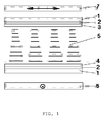
- the display device shown in Figure 1 comprises two transparent cell walls 1 enclosing a layer of nematic LC material 5 having positive dielectric anisotropy.
- the LC material 5 has dispersed within it nanoparticles 12 (shown in Figure 2) which tend to acquire either a negative or a positive charge by triboelectric charging in the LC.
- Each cell wall 1 has a transparent electrode 2, for example of indium tin oxide (ITO), on an inner surface thereof.
- the inner surface of one cell wall is provided with a first surface alignment layer 3, and the inner surface of the other cell wall is provided with a second surface alignment layer 4, each of which induces local planar alignment (parallel to the surface) in a specified azimuthal direction.
- ITO indium tin oxide
- the alignment direction induced by the first alignment layer 3 is at 45° to the alignment direction induced by the second alignment layer 4.
- the nematic director twists through one-eighth of a helix between the cell walls.
- the cell walls 1 are placed between crossed polarisers 6, 7 in such a manner that one of the planar alignment directions is parallel (or at 90° to) one of the polarisation directions, and consequently the other alignment direction is at 45° to both polarisation directions.
- Applying a first unipolar electrical pulse of suitable magnitude across the electrodes 2 causes the device to adopt a first homeoplanar alignment which is stable when the electric field is removed.
- Applying a second unipolar pulse of suitable magnitude, but opposite polarity to the first pulse causes the device to adopt a second homeoplanar alignment at 45° degrees to the first homeoplanar alignment.
- This second alignment is also stable when the electric field is removed so that the device is bistably switchable between each state.
- bistable switching Without wishing to be bound by theory, a possible mechanism for the bistable switching is discussed below.
- the cell adopts the homeoplanar orientation and, although it exhibits birefringence, between crossed polarisers this state is dark when the selected planar alignment is parallel to the input polariser, as transmission
- transm
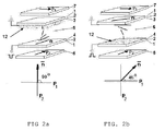
- FIG 2a where P1 and P2 show respectively the polarisation direction of crossed polarisers 7 and 6, and where n is the LC director orientation, the switching process is shows schematically.
- a negative pulse is applied to the lower electrode 2, causing negatively-charged nanoparticles 12 to collect close to the upper alignment layer 3.
- the lower alignment layer 4 has an orientation parallel to the polarisation direction P2 of polariser 6, through which input light enters the cell. In this configuration the display appears dark when viewed through the crossed polarisers 6, 7.
- An opposite connection of the unipolar pulse produces back switching (Figure 2b).
- the nanoparticles migrate and collect close to the opposite side (the lower alignment layer 4) and consequently the previous local homeotropic state reverts to the planar state, and the previous local planar alignment reverts to a local homeotropic state.
- the cell adopts a homeoplanar configuration, but this second homeoplanar configuration is oriented at 45° to the polarisers.
- the cell transmits light according to:
- transm
- o sin 2 2 ⁇ sin 2 (2 ⁇ d ⁇ n/ ⁇ ) .
- Reversing of the applied pulse provides switching to the previous state and the cell again adopts the dark state shown in Figure 2a.
- the cell has the same birefringence, determined by (2 ⁇ d ⁇ n/ ⁇ ), but the switching between light and dark states is provided by a rotation of the director n through 45° from one azimuthal direction to another.
- the cells have been constructed from two glass or plastic substrates with transparent ITO electrodes. Both of the substrates over the ITO electrode were covered by a thin layer, providing the planar alignment. Each alignment layer induces a local nematic director orientation at 45° with respect to each other. The thickness of the cell was controlled by polymer beads and varied from 2-15 ⁇ m. Commercial nematic LCs from Merck were used: E7, E63, MLC6204-000, ZLI2293, MLC6440 and MLC6023-000. These were doped by fumed silica or aluminium oxide.
- the negatively charged nanoparticles were silica Aerosil® R974, R106, R812, R711, R380, OX50 with primary size 7-40 nm and positively charged silica R504 (7 nm), aluminium oxide C (13 nm) (all from Degussa-Huls).
- the concentration of the particles in the LC was varied from 1-15% by total weight of the composition comprising LC and nanoparticles.
- Unipolar pulses with amplitude 10-80 V, and duration of the pulse 0.5-50 ms were applied to the cells.
- Figures 3a, 3b and 3c show the bistable switching between dark and light states in a 5 ⁇ m cell with nematic MLC6204-000 doped with 2% silica nanoparticles R812.
- Figure 3a shows optical transmittance registered by an oscilloscope
- Figures 3b and 3c show the corresponding dark and light states, observed under a polarising microscope.
- Figure 4 shows contrast ratio depending on the voltage of an applied electrical pulse of 4 ms duration
- Figure 5 plots contrast ratio against pulse length for an 80 V pulse (reset pulse 80V/4ms in both cases).
- Curves 8 and 10 show the switching from the initial dark state to the light state
- curves 9 and 11 show the switching from the initial light state to the dark state.
- a complex display may be addressed by means of conventional row and column electrodes, the construction of which is well known to those skilled in the art of LCD manufacture.
- each pixel defined by the intersection of a row and column electrode need be addressed only when its light transmission needs to be changed.
- the invention provides a bistable nematic display with good contrast and substantially symmetrical switching behaviour.
Landscapes
- Physics & Mathematics (AREA)
- Nonlinear Science (AREA)
- Chemical & Material Sciences (AREA)
- Optics & Photonics (AREA)
- Life Sciences & Earth Sciences (AREA)
- General Physics & Mathematics (AREA)
- Engineering & Computer Science (AREA)
- Crystallography & Structural Chemistry (AREA)
- Nanotechnology (AREA)
- Electrochemistry (AREA)
- Molecular Biology (AREA)
- Chemical Kinetics & Catalysis (AREA)
- Health & Medical Sciences (AREA)
- Biophysics (AREA)
- Liquid Crystal (AREA)
Applications Claiming Priority (1)
| Application Number | Priority Date | Filing Date | Title |
|---|---|---|---|
| GB0506193A GB2424716B (en) | 2005-03-29 | 2005-03-29 | Bistable liquid crystal display device |
Publications (2)
| Publication Number | Publication Date |
|---|---|
| EP1708017A2 true EP1708017A2 (de) | 2006-10-04 |
| EP1708017A3 EP1708017A3 (de) | 2007-01-24 |
Family
ID=34566522
Family Applications (1)
| Application Number | Title | Priority Date | Filing Date |
|---|---|---|---|
| EP06110613A Withdrawn EP1708017A3 (de) | 2005-03-29 | 2006-03-02 | Bistabile Flüssigkristallanzeigevorrichtung |
Country Status (3)
| Country | Link |
|---|---|
| US (1) | US7670654B2 (de) |
| EP (1) | EP1708017A3 (de) |
| GB (1) | GB2424716B (de) |
Cited By (2)
| Publication number | Priority date | Publication date | Assignee | Title |
|---|---|---|---|---|
| US8426020B2 (en) | 2006-12-14 | 2013-04-23 | Dsm Ip Assets B.V. | D1381 supercoatings for optical fiber |
| US8426021B2 (en) | 2006-12-14 | 2013-04-23 | Dsm Ip Assets B.V. | D 1364 BT secondary coatings on optical fiber |
Families Citing this family (2)
| Publication number | Priority date | Publication date | Assignee | Title |
|---|---|---|---|---|
| TWI423215B (zh) * | 2010-11-10 | 2014-01-11 | Au Optronics Corp | 雙穩態顯示器之驅動方法 |
| US20130321754A1 (en) * | 2012-05-30 | 2013-12-05 | Kent State University | Fumed Metal-Oxide Gel-Dispersed Blue-Phase Liquid Crystals and Devices Thereof |
Citations (1)
| Publication number | Priority date | Publication date | Assignee | Title |
|---|---|---|---|---|
| US20040144953A1 (en) | 2002-10-31 | 2004-07-29 | David Sikharulidze | Bistable nematic liquid crystal display device |
Family Cites Families (16)
| Publication number | Priority date | Publication date | Assignee | Title |
|---|---|---|---|---|
| US4305807A (en) * | 1980-03-13 | 1981-12-15 | Burroughs Corporation | Electrophoretic display device using a liquid crystal as a threshold device |
| JPS6186732A (ja) * | 1984-10-04 | 1986-05-02 | Canon Inc | 液晶装置 |
| JPH0561021A (ja) | 1990-10-08 | 1993-03-12 | Sanyo Chem Ind Ltd | 液晶材料及び液晶電気光学装置 |
| JPH04263217A (ja) * | 1990-10-12 | 1992-09-18 | Rudolf Eidenschink | 液晶媒体と、それを使用して映像を発生する方法 |
| JP2884462B2 (ja) * | 1993-08-31 | 1999-04-19 | キヤノン株式会社 | 液晶素子 |
| GB9402513D0 (en) * | 1994-02-09 | 1994-03-30 | Secr Defence | Bistable nematic liquid crystal device |
| JP3453956B2 (ja) * | 1995-01-31 | 2003-10-06 | 株式会社豊田中央研究所 | 液晶組成物 |
| GB9607854D0 (en) | 1996-04-16 | 1996-06-19 | Secr Defence | Liquid crystal device |
| US5956113A (en) * | 1997-01-31 | 1999-09-21 | Xerox Corporation | Bistable reflective display and methods of forming the same |
| JP4278297B2 (ja) * | 1997-10-08 | 2009-06-10 | ヒューレット・パッカード・カンパニー | 液晶装置の配向 |
| KR100641631B1 (ko) * | 2000-02-01 | 2006-11-02 | 엘지.필립스 엘시디 주식회사 | 쌍안정 액정 셀 및 그 제조방법 |
| US6992150B2 (en) * | 2000-03-13 | 2006-01-31 | Sanyo Chemical Industries, Ltd. | Toner binder and process for producing the same |
| EP1271225A1 (de) * | 2001-06-22 | 2003-01-02 | Hewlett-Packard Company, A Delaware Corporation | Bistabile nematische Flüssigkristallvorrichtung |
| SE0200910D0 (sv) * | 2002-03-22 | 2002-03-22 | Ecsibeo Ab | A liquid crystal device, a method for producing a liquid crystal device and a method for controlling liquid crystal device |
| GB0209917D0 (en) * | 2002-04-30 | 2002-06-05 | Hewlett Packard Co | Bistable nematic liquid crystal device |
| DE602004009170T2 (de) * | 2003-05-08 | 2008-07-03 | Merck Patent Gmbh | Flüssigkristallzusammensetzung zur verwendung in bistabilen flüssigkristallanzeigen |
-
2005
- 2005-03-29 GB GB0506193A patent/GB2424716B/en not_active Expired - Fee Related
-
2006
- 2006-03-02 EP EP06110613A patent/EP1708017A3/de not_active Withdrawn
- 2006-03-23 US US11/388,332 patent/US7670654B2/en active Active
Patent Citations (1)
| Publication number | Priority date | Publication date | Assignee | Title |
|---|---|---|---|---|
| US20040144953A1 (en) | 2002-10-31 | 2004-07-29 | David Sikharulidze | Bistable nematic liquid crystal display device |
Cited By (3)
| Publication number | Priority date | Publication date | Assignee | Title |
|---|---|---|---|---|
| US8426020B2 (en) | 2006-12-14 | 2013-04-23 | Dsm Ip Assets B.V. | D1381 supercoatings for optical fiber |
| US8426021B2 (en) | 2006-12-14 | 2013-04-23 | Dsm Ip Assets B.V. | D 1364 BT secondary coatings on optical fiber |
| US8734945B2 (en) | 2006-12-14 | 2014-05-27 | Dsm Ip Assets B.V. | D1364 BT secondary coatings on optical fiber |
Also Published As
| Publication number | Publication date |
|---|---|
| US20070222928A1 (en) | 2007-09-27 |
| GB0506193D0 (en) | 2005-05-04 |
| GB2424716B (en) | 2010-03-24 |
| EP1708017A3 (de) | 2007-01-24 |
| US7670654B2 (en) | 2010-03-02 |
| GB2424716A (en) | 2006-10-04 |
Similar Documents
| Publication | Publication Date | Title |
|---|---|---|
| Davidson et al. | Flexoelectric switching in a bistable nematic device | |
| US5327269A (en) | Fast switching 270° twisted nematic liquid crystal device and eyewear incorporating the device | |
| EP2024784A1 (de) | Mehrstabile reflektierende flüssigkristallanordnung | |
| EP1920027B1 (de) | Flüssigkristallanzeigevorrichtung | |
| US20050179632A1 (en) | Display element and display apparatus | |
| WO2008104533A1 (en) | Liquid crystal device | |
| US20080204612A1 (en) | Liquid crystal device | |
| US7430030B2 (en) | Bistable nematic liquid crystal display device | |
| US6151093A (en) | Liquid crystal display device having mixture to suppress changing switching characteristics with temperature of the liquid crystal display device | |
| US7264851B2 (en) | Bistable nematic liquid crystal display device | |
| US8462310B2 (en) | Bistable liquid crystal element | |
| EP1708017A2 (de) | Bistabile Flüssigkristallanzeigevorrichtung | |
| US7791706B2 (en) | Bistable nematic liquid crystal display device | |
| EP1962131B1 (de) | Flüssigkristallvorrichtung | |
| JPH09503601A (ja) | 高分子分散型強誘電性液晶表示装置 | |
| GB2407645A (en) | Electrophoretic liquid crystal display device | |
| KR100725218B1 (ko) | 듀얼모드 액정표시장치 및 그의 구동방법 | |
| US20040125294A1 (en) | Nematic liquid crystal bistable display device with grey level | |
| JP2002311436A (ja) | ネマチック液晶デバイスおよびその製造方法 | |
| KR20020062223A (ko) | 액정 디바이스 | |
| JPH0326368B2 (de) | ||
| KR100870789B1 (ko) | 그레이 수준을 가지는 네마틱 액정 쌍안정 디스플레이 장치 | |
| US20070222932A1 (en) | Bistable liquid crystal display device | |
| Sikharulidze et al. | 67.3: Electrophoretically Controlled Nematic LCD: Plastic Bistable Technology with Memorized Intrinsic Grey Scale | |
| JP2579636Y2 (ja) | 液晶表示素子 |
Legal Events
| Date | Code | Title | Description |
|---|---|---|---|
| PUAI | Public reference made under article 153(3) epc to a published international application that has entered the european phase |
Free format text: ORIGINAL CODE: 0009012 |
|
| AK | Designated contracting states |
Kind code of ref document: A2 Designated state(s): AT BE BG CH CY CZ DE DK EE ES FI FR GB GR HU IE IS IT LI LT LU LV MC NL PL PT RO SE SI SK TR |
|
| AX | Request for extension of the european patent |
Extension state: AL BA HR MK YU |
|
| PUAL | Search report despatched |
Free format text: ORIGINAL CODE: 0009013 |
|
| AK | Designated contracting states |
Kind code of ref document: A3 Designated state(s): AT BE BG CH CY CZ DE DK EE ES FI FR GB GR HU IE IS IT LI LT LU LV MC NL PL PT RO SE SI SK TR |
|
| AX | Request for extension of the european patent |
Extension state: AL BA HR MK YU |
|
| 17P | Request for examination filed |
Effective date: 20070720 |
|
| AKX | Designation fees paid |
Designated state(s): DE FR GB |
|
| 17Q | First examination report despatched |
Effective date: 20071018 |
|
| STAA | Information on the status of an ep patent application or granted ep patent |
Free format text: STATUS: THE APPLICATION IS DEEMED TO BE WITHDRAWN |
|
| 18D | Application deemed to be withdrawn |
Effective date: 20140703 |