EP1699081A1 - Solid-state imaging device, its production method, camera with the solid-state imaging device, and light-receiving chip - Google Patents
Solid-state imaging device, its production method, camera with the solid-state imaging device, and light-receiving chip Download PDFInfo
- Publication number
- EP1699081A1 EP1699081A1 EP04807285A EP04807285A EP1699081A1 EP 1699081 A1 EP1699081 A1 EP 1699081A1 EP 04807285 A EP04807285 A EP 04807285A EP 04807285 A EP04807285 A EP 04807285A EP 1699081 A1 EP1699081 A1 EP 1699081A1
- Authority
- EP
- European Patent Office
- Prior art keywords
- light
- solid
- state imaging
- receiving
- transparent protection
- Prior art date
- Legal status (The legal status is an assumption and is not a legal conclusion. Google has not performed a legal analysis and makes no representation as to the accuracy of the status listed.)
- Withdrawn
Links
Images










Classifications
-
- H—ELECTRICITY
- H10—SEMICONDUCTOR DEVICES; ELECTRIC SOLID-STATE DEVICES NOT OTHERWISE PROVIDED FOR
- H10F—INORGANIC SEMICONDUCTOR DEVICES SENSITIVE TO INFRARED RADIATION, LIGHT, ELECTROMAGNETIC RADIATION OF SHORTER WAVELENGTH OR CORPUSCULAR RADIATION
- H10F77/00—Constructional details of devices covered by this subclass
- H10F77/50—Encapsulations or containers
-
- H—ELECTRICITY
- H10—SEMICONDUCTOR DEVICES; ELECTRIC SOLID-STATE DEVICES NOT OTHERWISE PROVIDED FOR
- H10F—INORGANIC SEMICONDUCTOR DEVICES SENSITIVE TO INFRARED RADIATION, LIGHT, ELECTROMAGNETIC RADIATION OF SHORTER WAVELENGTH OR CORPUSCULAR RADIATION
- H10F39/00—Integrated devices, or assemblies of multiple devices, comprising at least one element covered by group H10F30/00, e.g. radiation detectors comprising photodiode arrays
- H10F39/80—Constructional details of image sensors
- H10F39/804—Containers or encapsulations
-
- H—ELECTRICITY
- H10—SEMICONDUCTOR DEVICES; ELECTRIC SOLID-STATE DEVICES NOT OTHERWISE PROVIDED FOR
- H10F—INORGANIC SEMICONDUCTOR DEVICES SENSITIVE TO INFRARED RADIATION, LIGHT, ELECTROMAGNETIC RADIATION OF SHORTER WAVELENGTH OR CORPUSCULAR RADIATION
- H10F39/00—Integrated devices, or assemblies of multiple devices, comprising at least one element covered by group H10F30/00, e.g. radiation detectors comprising photodiode arrays
- H10F39/80—Constructional details of image sensors
- H10F39/806—Optical elements or arrangements associated with the image sensors
-
- H—ELECTRICITY
- H04—ELECTRIC COMMUNICATION TECHNIQUE
- H04N—PICTORIAL COMMUNICATION, e.g. TELEVISION
- H04N23/00—Cameras or camera modules comprising electronic image sensors; Control thereof
- H04N23/50—Constructional details
-
- H—ELECTRICITY
- H10—SEMICONDUCTOR DEVICES; ELECTRIC SOLID-STATE DEVICES NOT OTHERWISE PROVIDED FOR
- H10F—INORGANIC SEMICONDUCTOR DEVICES SENSITIVE TO INFRARED RADIATION, LIGHT, ELECTROMAGNETIC RADIATION OF SHORTER WAVELENGTH OR CORPUSCULAR RADIATION
- H10F39/00—Integrated devices, or assemblies of multiple devices, comprising at least one element covered by group H10F30/00, e.g. radiation detectors comprising photodiode arrays
- H10F39/011—Manufacture or treatment of image sensors covered by group H10F39/12
- H10F39/026—Wafer-level processing
-
- H—ELECTRICITY
- H10—SEMICONDUCTOR DEVICES; ELECTRIC SOLID-STATE DEVICES NOT OTHERWISE PROVIDED FOR
- H10W—GENERIC PACKAGES, INTERCONNECTIONS, CONNECTORS OR OTHER CONSTRUCTIONAL DETAILS OF DEVICES COVERED BY CLASS H10
- H10W72/00—Interconnections or connectors in packages
- H10W72/20—Bump connectors, e.g. solder bumps or copper pillars; Dummy bumps; Thermal bumps
Definitions
- the present invention relates to a solid-state imaging apparatus, and particularly relates to a technology of reducing the size of an imaging apparatus and of improving productivity of such imaging apparatuses.
- Patent Reference 1 Japanese Laid-open patent application No. H7-086544 (hereinafter, Patent Reference 1) and Japanese Laid-open Patent ApplicationNo. H10-313070 (hereinafter, PatentReference2) disclose such conventional solid-state imaging apparatuses.
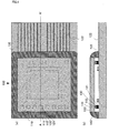
- FIG.1A is a plan view showing an overview of a conventional solid-state imaging apparatus 100 disclosed in the Patent Reference 1.
- the CCD chip 110 is shaped as a square. Eight input/output terminal pads 111 are provided along each of the right hand side and the left hand side of the square of the CCD chip 110. Underneath each of the input/output terminal pads 111, a bump 112 having a height of about 10 ⁇ m is provided.
- the glass substrate 120 is in a rectangular shape which is larger than the CCD chip 110. Sixteen electrode pads 121 (8 on the right hand side and 8 on the left hand side) are provided on the glass substrate 120, in position corresponding to the bumps 112 of the CCD chip 110 . Sixteen wirings 122 are formed on the upper surface of the glass substrate 120.
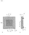
- FIG.2A is a plan view showing an overview of a conventional solid-state imaging apparatus 200 disclosed in the Patent Reference 2.
- FIG.2B is a diagram showing a cross sectional view of the solid-state imaging apparatus 200 of FIG.2A, which is cut at the line of A-A'.
- the conventional solid-state imaging apparatus 200 has the following structure.
- a chip bonding portion 211 is created as a concave groove, at the center of a base portion 210 (made of molded resin) of the solid-state imaging apparatus 200.
- a CCD chip 230 is attached via a silver paste 220.
- a bonding pad on the CCD chip 230 is connected to lead frames 240 via bonding wires 250.
- a sealing glass 270 is attached to the base portion 210 via a potting resin layer 260, so as to seal the CCD chip 230 together with the bonding wires 250 airtight.
- the glass substrate 120 is substantially larger, in area, than the CCD chip 110. This is because the glass substrate 120 has to have a part thereof to connect to an external device, at the surface thereof that faces towards the CCD chip 110 but does not overlap with the CCD chip 110 in position.
- the area of the glass substrate 120 is the major factor defining the area of the entire solid-state imaging apparatus 100, and so the area of the solid-state imaging apparatus is inherently larger than the area of the CCD chip 110.
- the base portion 210 and the sealing glass 270 are respectively larger, in area, than the CCD chip 230. Therefore, the exterior size of the base portion 210 or the sealing glass 270 is the major factor defining the exterior size of the entire solid-state imaging apparatus 200, and so the exterior size of the solid-state imaging apparatus 200 will be substantially larger than the exterior size of the CCD chip 230.
- the first object of the present invention is to reduce the size and the weight of the whole of a solid-state imaging apparatus, and further to contribute to reduction of size and weight of a camera to which the solid-state imaging apparatus is mounted, by reducing the area of a transparent protection plate such as a glass substrate, down to the area of a light-receiving chip or smaller, and by realizing a light-receiving chip that does not require a base portion through which mounting to an external device is performed.
- the area of the glass substrate 120 is clearly larger than the area of the CCD chip 110, and so attaching of the CCD chip 110 to the glass substrate 120 is performed after cutting a wafer into chips.
- thesolid-state imaging apparatus 200 of the Patent Reference 2 it is required to perform, after production of a wafer and cutting the wafer into chips, many steps to each chip such as a die bonding step, a wire bonding step, a potting resin layer application step, a seal glass attaching step, a potting resin layer hardening step, and a lead frame forming step, which degrades productivity.
- the second object of the present invention is to provide a solid-state imaging apparatus having excellent productivity, and a manufacturing method of such a solid-state imaging apparatus having excellent productivity, so as to realize cost reduction of a solid-state imaging apparatus, and further to realize cost reduction of a camera to which the solid-state imaging apparatus is mounted.
- a solid-state imaging apparatus is a solid-state imaging apparatus having: a light-receiving chip having a plurality of light-receiving cells arranged either one dimensionally or two dimensionally on one main surface of a base substrate; and a transparent protection plate attached to the main surface of the base substrate to cover the light-receiving cells, a space being formed between the light-receiving cells and the transparent protection plate, where an area of the transparent protection plate is equal to or smaller than an area of the light-receiving chip.
- a camera of the present invention has a solid-state imaging apparatus according to the present invention.
- a light-receiving chip according to the present invention is a light-receiving chip having: a plurality of light-receiving cells arranged either one dimensionally or two dimensionally on a first main surface of a base substrate; a plurality of input/output lines provided on the first main surface of the base substrate; a plurality of electrodes for connecting to outside devices, the electrodes being formed on a second main surface of the base substrate that is opposite to the first main surface; and a plurality of conductive units insulated from each other, each conductive unit electrically connecting one of the input/output lines with a corresponding one of the electrodes.
- a manufacturing method of solid-state imaging apparatus is amanufacturingmethodof solid-state imaging apparatuses each having: a light-receiving chip provided with a set of light-receiving cells arranged either one dimensionally or two dimensionally on one main surface of a base substrate; and a transparent protection plate, the manufacturing method including: a protection-plate preparing step of preparing a plurality of transparent protection plates each having an area that is equal to or smaller than an area of the light-receiving chip; an attaching step of attaching the prepared transparent protection plates onto a semiconductor wafer of light-receiving chips so that each set of light-receiving cells is covered by a corresponding one of the transparent protection plates, thereby generating an attached member in which the transparent protection plates are attached to the light-receiving chips; and a cutting step of cutting the attached member generated in the attaching step into respective solid-state imaging apparatuses.
- the area of a solid-state imaging apparatus is not larger than the area of a light-receiving chip. According to this characteristic, in a manufacturing process, it becomes possible to attach transparent protection plates to a wafer, and to thereafter cut them together into respective chips. The productivity of such a manufacturing process is much better than that of the conventional processes.
- the index of refraction in a space formed between a light-receiving cell and a corresponding transparent protection plate is smaller than the index of refraction of a collective lens normally provided on the light-receiving cell. Therefore, formation of the space enables favorable light-collective characteristics.
- the light-receiving chip further has: a plurality of input/output lines provided on the main surface of the base substrate on which the light-receiving cells are arranged, the main surface being a first main surf ace; a plurality of electrodes for connecting to outside devices, the electrodes being provided on a second main surface of the base substrate that is opposite to the first main surface; and a plurality of conductive units insulated from each other, each conductive unit electrically connecting one of the input/output lines with a corresponding one of the electrodes.
- the electrodes for outside connection are provided on the second main surface that is different from the first main surface. Accordingly, it becomes possible to reduce the area of a transparent protection plate to be equal to or smaller than the area of a light-receiving chip. This further leads to reduction of size and weight of an entire solid-state imaging apparatus, which contributes to reduction of size and weight of a camera.
- the distance between a surface of a light-receiving chip and a transparent protection plate should be at least about the height of the bonding wire, so as to prevent the bonding wire from interfering with the light-receiving chip or with the transparent protection plate.
- the stated structure does not require a bonding wire, and that the distance may be equal to or smaller than the height of a bondingwire, which enables the thickness of a solid-state imaging apparatus to be thinner than conventionally. This creates a multiplier effect with the area reduction effect stated above, in reducing the size of a camera.
- each of the conductive units is a through hole provided through the base substrate.
- a through hole is generated instead of a conventional bonding pad. Therefore, the designing is performed without any regard to the conventional designing rule that depends on the accuracy of a wire bonding apparatus, and the like.
- each of the electrodes is provided on an opening of a corresponding through hole on the second main surface.
- each of the conductive units is a wiring formed on a side surface of the base substrate.
- a wiring pattern is provided for a side surface, instead of provision of a conventional bonding pad. Therefore the entire area of a bonding pad becomes unnecessary. Therefore, the designing is performed without any regard to the conventional designing rule that depends on the accuracy of a wire bonding apparatus, and the like.
- the light-receiving chip further has: a plurality of input/output lines provided on the main surface of the base substrate on which the light-receiving cells are arranged, the main surface being a firstmainsurface; a plurality of electrodes for connecting to outside devices, the electrodes being formed on a second main surface of the base substrate that is opposite to the first main surface; and a plurality of conductive units insulated from each other, each conductive unit electrically connecting one of the input/output lines with a corresponding one of the electrodes; and a plurality of collective lenses provided on a light-receiving of the onemain surface of the base substrate, where the space is formed between the collective lenses and the transparent protection plate, and an index of refraction of the space is smaller than an index of refraction of the
- the electrodes for outside connection are provided on the second main surface that is different from the first main surface (the first main surface being the light-receiving surface for the light-receiving chip). Therefore, the area of a transparent protection plate is able to be reduced to equal to or smaller than the area of a light-receiving chip. Therefore, the entire solid-state imaging apparatus is able to be reduced in size and weight, which contributes to reduction in size and weight of a camera.
- the solid-state imaging apparatus further has: a sealing material operable to fix the base substrate and the transparent protection plate, where the first main surface is made up of the light-receiving area on which the light-receiving cells are arranged and a periphery area surrounding the light-receiving area, the sealing material being provided on the periphery area, and the space is sealed airtight by means of the base substrate, the transparent protection plate, and the sealing material.
- the light-receiving area is sealed airtight, and so is prevented from dust or from corrosion.
- the main surface is made up of a light-receiving area on which the light-receiving cells are arranged and a periphery area surrounding the light-receiving area
- the transparent protection plate has a skirt portion at a periphery thereof, and the skirt portion is attached onto the periphery area of the main surface, thereby sealing the light-receiving cells airtight and forming the space between the light-receiving cells and the transparent protection plate.
- the distance between the light-receiving area and the transparent protection plate depends on the accuracy of the form of the transparent protection plate. Therefore, the distance hardly varies, which contributes to productivity improvement.
- the skirt portion is formed by plating metal on the periphery of the transparent protection plate that is a flat plate made of glass or resin.
- the transparent protection plate is a flat plate made of resin, and the skirt portion is formed by pressing the flat resin plate. According to the stated structures, manufacturing enables the distance between the light-receiving area and the transparent protection plate to be in the accuracy of about several ⁇ m.
- the main surface is made up of a light-receiving area on which the light-receiving cells are arranged and a periphery area surrounding the light-receiving area
- the light-receiving chip has, on the periphery area of the main surface, a rib portion having a loop shape, the rib portion is attached onto a periphery of the transparent protection plate, thereby sealing the light-receiving cells airtight and forming the space between the light-receiving cells and the transparent protection plate.
- the distance between the light-receiving area and the transparent protection plate depends on the accuracy of the form of the light-receiving chip. Therefore, the distance hardly varies, which contributes to productivity improvement.
- the rib portion is an insulator made of a material for protective foil.
- manufacturing enables the distance between the light-receiving area and the transparent protection plate to be in the accuracy of about several ⁇ m. Furthermore, rib-portion forming is performed in the diffusion process that is prior to the chip-cutting process, and so no extra process is required for the rib-portion forming, which contributes to productivity improvement.
- the solid-state imaging apparatus and the camera being manufactured by attaching transparent protection plates onto a semiconductor wafer of light-receiving chips to generate an attached member in which the transparent protection plates are attached to the light-receiving chips respectively, and cutting the attached member into respective solid-state imaging apparatuses.
- the transparent protection plates are attached to the wafer, and then the resulting attached member is cut into respective chips, which contributes to great productivity improvement compared to conventional cases. Accordingly, it becomes possible to reduce the price of a solid-state imaging apparatus, which further contributes to price reduction of a camera.
- the solid-state imaging apparatus and the camera being manufactured by simultaneously cutting out the light-receiving chip and the transparent protection plate, as a set.
- only one process is required for cutting out a set of light-receiving chip and transparent protection plate. This is a reduction in number of processes, and also enables to easily obtain a clean cross section for a set of light-receiving chip and transparent protection plate.
- the main surface has a light-receiving area in a central portion thereof, and a plurality of electrodes outside the light-receiving area
- the transparent protection plate includes: a plurality of terminal pads formed on the other main surface that is different from the main surface; and a plurality of conductive members insulated from each other, each conductive member electrically connecting one of the electrodes with a corresponding one of the terminal pads.
- the present disclosure it becomes possible to restrain the lengthwise/widthwise size of an entire solid-state imaging apparatus down to the lengthwise/widthwise size of a corresponding solid-state imaging device.
- the thickness of an entire solid-state imaging apparatus is also restrained down to substantially the summation of the thickness of the solid-state imaging device and the thickness of a corresponding transparent protection plate.
- the solid-state imaging apparatus will be much smaller, in size, than conventional solid-state imaging apparatuses.
- a plurality of holes are provided through the transparent protection plate, the holes being provided in position that will not prevent light from traveling onto the light-receiving area, and part of each of the conductive members is positioned in a corresponding one of the holes.
- the part of each of the conductive members that is positioned in the corresponding hole is a conductive foil attached to a side wall of the of the corresponding hole.
- the part of each of the conductive members that is positioned in the corresponding hole is a conductive material filling the corresponding hole.
- each of the conductive members is a conductive foil attached to the main surface, a side surface, and the other main surface of the transparent protection plate.
- a conductive foil is provided on a side surface, instead of provision of a conventional bonding pad. Therefore the entire area of a bonding pad becomes unnecessary. Therefore, the designing is performed without any regard to the conventional designing rule that depends on the accuracy of a wire bonding apparatus, and the like. Accordingly, it is possible to have expectations that the area of the light-receiving chip be reduced because the structures allow greater layout flexibility, which contributes to reduction in size and weight of a camera.
- a camera according to the present invention is a solid-state imaging apparatus of Claim 1; and a print wiring board having lands arranged to correspond, in position, to terminals of the solid-state imaging apparatus, where each of the terminals is flip-chip mounted directly to a corresponding one of the lands.
- the thickness of a solid-state imaging apparatus is able to be restrained to substantially the summation of the thickness of a solid-state imaging device and the thickness of a transparent protection plate.
- the transparent protection plates are attached to the wafer, and then the resulting attached member is cut into respective chips, which contributes to great productivity improvement compared to conventional cases. Accordingly, it becomes possible to reduce the price of a solid-state imaging apparatus, which further contributes to price reduction of a camera.
- a corresponding main surface is made up of a light-receiving area on which a set of light-receiving cells are arranged and a periphery area surrounding the light-receiving area
- each of the transparent protection plates prepared in the protection-plate preparing step has a skirt portion at a periphery of the transparent protection plate
- a corresponding set of light-receiving cells of a solid-state imaging apparatus is sealed airtight by a skirt portion of a corresponding transparent protection plate that is attached onto a corresponding periphery area, so as to form a space between the set of light-receiving cells and the transparent protection plate.
- each of the transparent protection plates is a flat plate made of glass or resin, and in the protection-plate preparing step, a corresponding skirt portion is created by plating metal on the periphery of each of the transparent protection plates.
- each of the transparent protection plates is a flat plate made of resin, and in the protection-plate preparing step, a corresponding skirt portion is created by pressing the flat resin plate. According to the stated structures, manufacturing enables the distance between the light-receiving area and the transparent protection plate to be in the accuracy of about several ⁇ m.
- the distance between the light-receiving area and the transparent protection plate depends on the accuracy of the form of the light-receiving chip. Therefore, the distance hardly varies, which contributes to productivity improvement.
- a rib portion of a corresponding light-receiving chip is made of an insulative material that is the same as a material of a protection foil. According to the stated structure, manufacturing enables the distance between the light-receiving area and the transparent protection plate to be in the accuracy of about several ⁇ m.
- rib-portion forming is performed in the diffusion process that is prior to the chip-cutting process, and so no extra process is required for the rib-portion forming, which contributes to productivity improvement.
- the protection-plate preparing step a sheet in which the plurality of transparent protection plates are linked together is prepared, in the attaching step, the sheet of the transparent protection plates is attached onto the plurality of light-receiving chips in the state of the semiconductor wafer, and in the cutting step, a light-receiving chip and a corresponding transparent protection plate is cut out as a set simultaneously.
- FIG.1A is a plan view showing an overview of a conventional solid-state imaging apparatus 100 disclosed in the Patent Reference 1.
- FIG.2B is a diagram showing a cross sectional view of the solid-state imaging apparatus 200 of FIG.2A, which is cut at the line of A-A'.
- FIG.4B is a diagram showing a sectional view of a transparent protection plate 12 that results by forming a skirt portion by subjecting acrylic resin and the like to press forming, so that the periphery portion of the transparent protection plate 12 is thicker than the central portion thereof by "thickness of collective lens 16 + ⁇ ".
- FIG. 6B is a diagram showing a sectional view of the solid-state imaging apparatus 30 which is cut at the line A-A' of FIG.6A.
- FIG.8B is a diagram showing a sectional view of the solid-state imaging apparatus 40 which is cut at the line A-A' of FIG.8A.
- FIG.11B is a diagram showing a sheet of transparent protection plate 12, which is generated by Step S6 of the manufacturing method 1.
- FIG.13B is a diagram showing a sheet of transparent protection sheet 12 generated in Step S16 of the manufacturing method 2.
- FIG 15B is a diagram showing a sheet of transparent protection plate 12 generated in Step S26 of the manufacturing method 3.
- FIG.26B is a plan view showing an overall structure of a transparent protection plate linkage member 330 in which a plurality of transparent protection plates 306 are linked to each other on one plane.
- FIG.3A is a plan view showing a solid-state imaging apparatus 10 according to the embodiment 1 of the present invention.
- FIG. 3B is a diagram showing a sectional diagramof the solid-sate imaging apparatus 10, which is cut at the line A-A' of FIG.3A.
- the solid-state imaging apparatus 10 of the embodiment 1 is made up of a solid-state imaging device 11, a transparent protection plate 12, and a sealing material 13.
- the solid-state imaging device 11 is a light-receiving chip such as a CCD chip and a MOS chip, for example.
- the solid-state imaging device 11 includes a base substrate 14, electrodes 15, collective lenses 16, and through holes 17.
- the first main surface of the base substrate 14 is divided into a light-receiving area 18 and a periphery area 19 (the first main surface corresponds to the upper surface in FIG.3B, and is hereinafter referred to as "light-receiving surface").
- the light-receiving area 18 is provided with a plurality of light-receiving cells arranged either one dimensionally or two dimensionally, where each light-receiving cell corresponds to one pixel.
- the periphery area 19 is an area positioned around the periphery of the light-receiving area, into which circuits other than the light-receiving cells are integrated.
- light-receiving cells corresponding to 300,000 pixels are arranged two dimensionally in the light-receiving area:
- the base substrate 14 is conventionally a semiconductor substrate made of silicon. Areas of the base substrate 14 that are in contact with the electrodes 15, the through holes 17, the input/output lines, and the like are covered by an insulation material such as silicon oxide and silicon nitride.
- the electrodes 15 are formed on the second main surface of the base substrate 14 in the vicinity of the through holes 17 for outside connection.
- An example of an electrode 15 is a bump.
- the second main surface is positioned at the back of the light-receiving surface (the lower surface in FIG.3B) and so is hereinafter referred to as "back surface”.
- the electrodes 15 are used to connect to corresponding terminals of a circuit substrate in mounting the solid-state imaging apparatus 10 to the circuit substrate.
- Each of the collective lenses 16 is provided on the light-receiving area 18, and functions to collect a projected image on the light-receiving area 18 by means of a corresponding light-receiving cell. The collective lenses 16 enhance light-receiving sensitivity.
- the through holes 17 are respectively a conductive member electrically connecting the light-receiving surface and the back surface.
- the through holes 17 are insulated one from another, and each insulated through hole 17 connects a corresponding one of the input/output lines to a corresponding one of the electrodes 15.
- the number of the electrodes 15 and the number of the through holes 17 are respectively equal to the number of the input/output lines provided on the light-receiving surface. In the present embodiment, there are twenty electrodes 15, twenty through holes 17, and twenty input/output lines.
- the transparent protection plate 12 is made of glass or acrylic resin, for example, which is able to transmit incident light without considerably changing the optical characteristics of the incident light.
- the transparent protection plate 12 is attached to the base substrate to entirely cover the light-receiving cells.
- the transparent protection plate 12 functions to protect the light-receiving area 18 and the collective lenses 16 of the solid-state imaging device 11 from physical damage and from dust. It should be noted here that the area of the transparent protection plate 12 may be equal to or smaller than the area of the solid-state imaging device 11. In the present embodiment, the transparent protection plate 12 and the solid-state imaging device 11 have substantially the equal area.
- the sealing material 13 fixes, at the periphery area 19, the base substrate 14 and the transparent protection plate 12.
- the transparent protection plate 12 has a periphery portion that is thick and is in a loop shape (hereinafter "skirt portion").
- the transparent protection plate 12 has such a concave shape that the part thereof covering the light-receiving area 18 is recessed with respect to the part thereof corresponding to the periphery area 19.
- the skirt portion of the transparent protection plate 12 is attached to the periphery area 19 by means of the sealing material 13, thereby sealing the light-receiving cells airtight and forming a space 20 between the collective lenses 16 and the transparent protection plate 12.
- the solid-state imaging device 11 may have a protrusion having a loop shape, in the periphery area 19 (the loop-shaped protrusion being hereinafter referred to as "rib portion"), so that the periphery area 19 protrudes with respect to the light-receiving area 18.
- the periphery of the transparent protection plate 12 is attached to the rib portion of the solid-state imaging device 11 by means of the sealing material 13, thereby sealing the light-receiving cells airtight and forming the space 20 between the collective lenses 16 and the transparent protection plate 12.
- the index of refraction of the space 20 is smaller than the index of refraction of the collective lens 16.
- the index of refraction for the space 20 is about 1.0.
- the space 20 is filled with air or inert gas.
- the space 20 may be in a vacuum state, in a sense that the space 20 is under pressure lower than atmospheric pressure.
- the collective lenses 16 may be made of a material having an index of refraction of about 2.0 or more, and the space 20 may be filled with resin having an index of refraction of about 1.5, for example.
- the air with which the space 20 is filled should desirably be dry air, and the inert gas is specifically helium, neon, argon, nitride, a mixture of them, and the like.
- the minimum size for the distance between the collective lenses 16 and the transparent protection plate 12 is " ⁇ " that only takes into account accuracy such as variation of components and production accuracy.
- the distance between the base substrate 14 and the transparent protection plate 12 will be "thickness of collective lens 16 + ⁇ " , which is equal to or smaller than the height of abonding wire, which would be required for preventing interference with a bonding wire in a conventional type that uses a bonding wire.
- " ⁇ " is several ten times of the accuracy such as variation of components and production accuracy. For example, when the accuracy is about several ⁇ m, then the value of " ⁇ " may be about several 10 ⁇ m - 100 ⁇ m.
- FIG. 4A is a diagram showing a sectional view of a transparent protection plate 12 that results by forming, using a plating method, a skirt portion (metal 12b) to a periphery portion of a flat plate 12a made of glass or acrylic resin, and the like. As shown in this drawing, the periphery portion of the transparent protection plate 12 is thicker than the central portion thereof by "thickness of collective lens 16 + ⁇ ".
- FIG.4B is a diagram showing a sectional view of a transparent protection plate 12 that results by forming a skirt portion by subjecting acrylic resin and the like to press forming, so that the periphery portion of the transparent protection plate 12 is thicker than the central portion thereof by "thickness of collective lens 16 + ⁇ ".
- FIG.4C is a diagram showing a sectional view of a solid-state imaging device 11 whose periphery area 19 is provided with a rim portion, thereby causing the periphery portion of the solid-state imaging device 11 to be thicker than the central portion by "thickness of collective lens 16 + ⁇ ".
- the rim portion is formed in the diffusion process, using an insulation material 11a that is the same material as used for a protection foil such as a nitride foil and an oxide foil.
- FIG. 5 is a diagram showing a sectional view of the solid-state imaging device 11 in the vicinity of one of the through holes 17.
- a hole 21 is provided through the base substrate 14, and both main surfaces of the base substrate 14 and the inside the hole 21 are coated with an insulation material 22. Furthermore, the input/output line 23 provided up to the vicinity of the hole 21 on the light-receiving surface (upper surface of FIG.5) is electrically connected to the conductive member 25 at a contact portion 24.
- the conductive member 25 is provided through the base substrate 14 by penetrating through the hole 21 from the light-receiving surface to the back surface of the base substrate 14 (lower surface of FIG.5), to form a pad 26 for an electrode 15.
- the hole 21 is filled with a filling material 27, and the electrode 15 is formed on the pad 26 formed on the back surface.
- a conductive member 25 may be used to fill the entire hole.
- FIG. 6A is a plan view showing a solid-state imaging apparatus 30 according to the modification example 1 of the present invention.
- FIG. 6B is a diagram showing a sectional view of the solid-state imaging apparatus 30 which is cut at the line A-A' of FIG.6A.
- the solid-state imaging apparatus 30 according to the modification example 1 is made up of a solid-state imaging device 31, a transparent protection plate 12, and a sealing material 13.
- the solid-state imaging device 31 is-a light-receiving chip such as a CCD chip and a MOS chip, for example, just as in the embodiment 1.
- the solid-state imaging device 31 includes a base substrate 14, electrodes 32, collective lenses 16, and through holes 17.
- the electrodes 32 are on the back surface and immediately above the through holes 17, unlike in the solid-state imaging device 11 of the embodiment 1, and the structure in the vicinity of the through holes 17 is different from in the case of the solid-state imaging device 11 of the embodiment 1.
- Each of the electrodes 32 for outside connection is formed on the back surface above a corresponding one of the through holes 17.
- An example of an electrode 32 is a bump.
- the electrodes 32 are used to connect to corresponding terminals of a circuit substrate in mounting the solid-state imaging apparatus 30 to the circuit substrate.
- FIG.7 is a diagram showing a detailed sectional view of the solid-state imaging device 31 in the vicinity of one of the through holes 17, according to the modification example 1 of the present invention.
- a hole 21 is provided through the base substrate 14 made of silicon, and both main surfaces of the base substrate 14 and the inside the hole 21 are coated with an insulation material 22.
- the input/output line 23 provided up to the vicinity of the hole 21 on the light-receiving surface (upper surface of FIG.
- the conductive member 33 is provided through the base substrate 14 by penetrating through the hole 21 from the light-receiving surface to the back surface of the base substrate 14 (lower surface of FIG.7).
- the hole 21 is filled with a filling material 27, and the electrode 32 is formed on the back surface and above the hole 21.
- FIG.8A is a plan view showing a solid-state imaging apparatus 40 according to the modification example 2 of the present invention.
- FIG.8B is a diagram showing a sectional view of the solid-state imaging apparatus 40 which is cut at the line A-A' of FIG.8A.
- the solid-state imaging apparatus 40 is made up of a solid-state imaging device 41, a transparent protection plate 12, and a sealing material 13.
- the solid-state imaging device 41 is a light-receiving chip such as a CCD chip and a MOS chip, for example, just as in the embodiment 1.
- the solid-state imaging device 41 includes a base substrate 42, electrodes 43, collective lenses 16, and conductive wires 45.
- the electrodes 43 for outside connection are formed on the back surface.
- An example of an electrode 43 is a bump.
- the electrodes 43 are used to connect to corresponding terminals of a circuit substrate in mounting the solid-state imaging apparatus 40 to the circuit substrate.
- the conductive wires 45 are conductive members formed on the side surfaces of the base substrate 42, and are used to electrically connect the light-receiving surface to the back surface.
- the conductive wires 45 are insulated one from another, and each insulated conductive wire electrically connects a corresponding one of the input/output lines to a corresponding one of the electrodes 15.
- the number of the electrodes 43 and the number of the conductive wires 45 are equal to the number of the input/output lines provided on the light-receiving surface.
- FIG.9 is a diagram showing a detailed sectional view of the solid-state imaging device 41 in the vicinity of one of the conductive wires 45, according to the modification example 2 of the present invention.
- both of the main surfaces and the side surfaces of the base substrate 42 are coated with an insulation material 46.
- the input/output line 47 provided on the light-receiving surface (upper surface of FIG.9) up to the vicinity of the side surface 44 of the base substrate 42 is electrically connected to the conductive member 49 at a contact portion 48.
- the conductive member 49 is provided from the light-receiving surface via the side surface 44 up to the back surface (lower surface of FIG. 9) of the base substrate 42, to form a pad 50 for an electrode 43.
- the electrode 43 is formed on the pad 50 on the back surface.
- FIG.10 is a diagram showing an overview of a manufacturing method of a solid-state imaging apparatus 10, in the case where the skirt portion of the transparent protection plate 12 is formed by a plating method (see FIG.4A). The following describes the overview of the manufacturing method of the solid-state imaging apparatus 10 with reference to FIG.4A, FIG.5, and FIG.10.
- Step S1 a semiconductor wafer is processed, thereby forming a wafer for solid-state imaging device.
- Electrodes 15 are formed to the wafer (Step S5).
- a sheet of solid-state imaging device 11 completes.
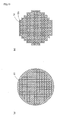
- FIG.11A is a diagram showing a sheet of solid-state imaging device 11, which is generated by Steps S1-S5 of the manufacturing method 1.
- FIG.11B is a diagram showing a sheet of transparent protection plate 12, which is generated by Step S6 of the manufacturing method 1.
- the sheet of transparent protection plate 12 has, at respective periphery portions, skirt portions made of the metal 12b.
- the sheet of solid-state imaging device 11 is not provided with any protrusions, as FIG.11A shows.
- Step S7 the sheet of transparent protection plate 12 (resulting from Step S6) is attached onto the sheet of solid-state imaging device 11 (resulting from Steps S1-S5).
- Step S7 a sheet of solid-state imaging apparatus 10 completes.
- FIG.12 is a diagram showing an overview of a manufacturing method of a solid-state imaging apparatus 10, in the case where the skirt portion of the transparent protection plate 12 is formed by subjecting acrylic resin and the like to press forming (See FIG.4B). The following describes the overview of the manufacturing method of the solid-state imaging apparatus 10 with reference to FIGs.4B, FIG.5, and FIG.12.
- Step S11 (1) In a diffusion process, a semiconductor wafer is processed, thereby forming a wafer for solid-state imaging device.
- FIG.13A is a diagram showing a sheet of solid-state imaging device 11 generated in Steps S11-S15 of the manufacturing method 2.
- FIG.13B is a diagram showing a sheet of transparent protection sheet 12 generated in Step S16 of the manufacturing method 2. As FIG.13B shows, a skirt portion 12c is formed to each periphery portion of the sheet of transparent protection sheet 12. In contrast, the sheet of solid-state imaging device 11 is not provided with any protrusions, as FIG.13A shows.
- Step S18 thesheetofsolid-state imaging apparatus 10 generated in Step S17 is cut into chips.
- a dicing saw is used to dice the sheet of solid-state imaging apparatus 10 into respective sets of solid-state imaging device 11 and transparent protection plate 12.
- FIG.14 is a diagram showing an overview of a manufacturing method of a solid-state imaging apparatus 10, in the case where the rib portion of the solid-state imaging device 11 is formed in the diffusion process (see FIG.4C).
- FIG.15A is a diagram showing the sheet of solid-state imaging device 11 generated in Steps S21-25 of the manufacturing method 3.
- FIG 15B is a diagram showing a sheet of transparent protection plate 12 generated in Step S26 of the manufacturing method 3.
- rib portions are formed to respective periphery portions of the sheet of solid-state imaging device 11.
- the sheet of transparent protection plate 12 is not provided with any thick portions, as FIG.15B shows.
- Step S28 the sheet of solid-state imaging apparatus 10 generated in Step S27 is cut into chips.
- a dicing saw is used to dice the sheet of solid-state imaging apparatus 10 into respective sets of solid-state imaging device 11 and transparent protection plate 12.
- the input/output lines on the light-receiving surface are electrically connected to the electrodes for outside connection provided on the back surf ace. Therefore, input (e.g. an electric power or a control signal) from an external circuit substrate is received by the electrodes for outside connection provided on the back surface, and the received input is transferred to the input/output lines on the light-receiving surface, via the conductive member, so as to drive the solid-state imaging device.
- output e.g. an image signal
- the area of the transparent protection plate is made equal to or smaller than the area of the light-receiving chip, which helps reduce the size and the weight of a camera to which the solid-state imaging apparatus of the present invention is to be mounted.
- the distance between the light-receiving chip and the transparent protection plate is made smaller than in the conventional cases. This creates a multiplier effect with the area reduction effect stated above, in reducing the size and weight of a camera to which the solid-state imaging apparatus of the present invention is to be mounted.
- the embodiment 1, the modification example 1, and the modification example 2 of the present invention enable the productivity to considerably improve compared to conventional cases, because the entire area of the solid-state imaging apparatus is not larger than the area of the light-receiving chip, and so a wafer for light-receiving chip, as it is, is able to be attached to a sheet of transparent protection plates, before being cut into respective chips.
- the distance between a transparent protection plate and a corresponding light-receiving area is designed to depend on the accuracy of the forms respectively of the transparent protection plate and the light-receiving chip. Accordingly, this distance will hardly vary, which contributes to productivity improvement.
- FIG. 16A is a plan view showing a solid-state imaging apparatus 60 according to the embodiment 2 of the present invention.
- FIG.16B is a diagram showing a sectional view of the solid-state imaging apparatus 60, which is cut at the line A-A' of FIG.16A.
- the solid-state imaging apparatus 60 of the embodiment 2 is made up of a solid-state imaging device 61, a transparent protection plate 62, and a sealing material 63.
- the solid-state imaging device 61 is a light-receiving chip such as a CCD chip and a MOS chip, for example.
- the solid-state imaging device 61 includes a base substrate 64, electrodes 65, and collective lenses 66.
- the first main surface of the base substrate 64 is divided into a light-receiving area 68 and a periphery area 69 (the first main surface corresponds to the upper surface in FIG.16B, and is hereinafter referred to as "light-receiving surface").
- the light-receiving area 68 is provided with a plurality of light-receiving cells arranged either one dimensionally or two dimensionally, where each light-receiving cell corresponds to one pixel.
- the periphery area 69 is an area positioned around the periphery of the light-receiving area, into which circuits other than the light-receiving cells are integrated.
- light-receiving cells corresponding to 300,000 pixels are arranged two dimensionally in the light-receiving area.
- the base substrate 64 is conventionally a semiconductor substrate made of silicon. Areas of the base substrate 64 that are in contact with the electrodes 65, the input/output lines, and the like are covered by an insulation material such as silicon oxide and silicon nitride.
- the electrodes 65 for outside connection are formed on the periphery area 69 on the light-receiving surface of the base substrate 64. The electrodes 65 are used to connect to corresponding terminals of a circuit substrate in mounting the solid-state imaging apparatus 60 to the circuit substrate.
- Each of the collective lenses 66 is provided on the light-receiving area 68, and functions to collect a projected image on the light-receiving area 68 by means of a corresponding light-receiving cell.
- the collective lenses 66 enhance light-receiving sensitivity.
- the number of the electrodes 65 is equal to the number of the input/output lines provided on the light-receiving surface. In the present embodiment, there are twenty electrodes 65 and twenty input/output lines.
- the transparent protection plate 62 is made of glass or acrylic resin, for example, which is able to transmit incident light without considerably changing the optical characteristics of the incident light.
- the transparent protection plate 62 is attached to the base substrate 64 to entirely cover the light-receiving cells, without covering the electrodes 65 at all.
- the transparent protection plate 62 functions to protect the light-receiving area 68 and the collective lenses 66 of the solid-state imaging device 61 from physical damage and from dust. It should be noted here that the area of the transparent protection plate 62 is smaller than the area of the solid-state imaging device 61.
- the sealing material 63 fixes, at the periphery area 69, the base substrate 64 and the transparent protection plate 62.
- the transparent protection plate 62 has a skirt portion at its periphery portion.
- the transparent protection plate 62 has such a concave shape that the part thereof covering the light-receiving area 68 is recessed with respect to the part thereof corresponding to the periphery area 69.
- the skirt portion of the transparent protection plate 62 is attached to the periphery area 69 by means of the sealing material 63, thereby sealing the light-receiving cells airtight and forming a space 70 between the collective lenses 66 and the transparent protection plate 62.
- the solid-state imaging device 61 may have a rib portion in the periphery area 69, so that the periphery area 69 protrudes with respect to the light-receiving area 68.
- the periphery of the transparent protection plate 62 is attached to the rib portion of the solid-state imaging device 61 by means of the sealing material 63, thereby sealing the light-receiving cells airtight and forming the space 70 between the collective lenses 66 and the transparent protection plate 62.
- the characteristics of the space 70 is the same as those of the space 20 explained in the embodiment 1, and so detailed description thereof is omitted.
- the distance between the collective lenses 66 and the transparent protection plate 62 is also identical to the distance between the collective lenses 16 and the transparent protection plate 12 regarding the space 20. Since the distance regarding the space 20 has already been discussed in the embodiment 1, and so discussion of the distance regarding the space 70 is accordingly omitted.
- FIG.17 is a diagram showing an overview of a manufacturing method of a solid-state imaging apparatus 60, in the case where the skirt portion of the transparent protection plate 62 is formed by a plating method (See FIG.4A).
- Step S42 a sheet of transparent protection plate 62 completes, which is made up of a plurality of transparent protection plates, each transparent protection plate having an area that is equal to or smaller than an area of one solid-state imaging device 61.
- Step S43 the sheet of transparent protection plate 62 generated in Step S42 is cut into chips
- Step S44 a sheet of solid-state imaging apparatus 60 completes.
- respective skirt portions are formed by subjecting a sheet made of acrylic resin and the like to press forming, so as to complete a sheet of transparent protection plate 62, which is made up of a plurality of transparent protection plates, each transparent protection plate having an area that is equal to or smaller than an area of one solid-state imaging device 61, and whose periphery portions are thicker than the central portions (Step S52).
- Step S54 transparent protection plates 62 (resulting from Step S53) are respectively attached onto solid-state imaging devices 61 of the sheet of solid-state imaging device 61 (resulting from Step S51).
- Step S54 a sheet of solid-state imaging apparatus 60 completes.
- FIG.19 is a diagram showing an overview of a manufacturing method of a solid-state imaging apparatus 60, in the case where the rib portion of the solid-state imaging device 61 is formed in the diffusion process. The following describes the overview of the manufacturing method of the solid-state imaging apparatus 60 with reference to FIG.19.
- Step S61 a sheet of solid-state imaging device 61 completes.
- a flat plate made of glass, acrylic resin, and the like is used to form a sheet of transparent protection plate 62, which is made up of a plurality of transparent protection plates, each transparent protection plate having an area that is equal to or smaller than an area of one solid-state imaging device 61 (Step S62).
- Step S64 transparent protection plates 62 resulting from Step S63 are respectively attached onto solid-state imaging devices 61 of the sheet of solid-state imaging device 61 (resulting from Step S61).
- Step S64 a sheet of solid-state imaging apparatus 60 completes.
- the embodiment 2 of the present invention enables the productivity to considerably improve compared to conventional cases, because the entire area of the solid-state imaging apparatus is not larger than the area of the light-receiving chip, and so transparent protection plates are attached onto a wafer of light-receiving chip and then the resulting attached member is cut into respective chips.
- the distance between a transparent protection plate and a corresponding light-receiving area is designed to depend on the accuracy of the forms respectively of the transparent protection plate and the light-receiving chip. Accordingly, this distance will hardly vary, which contributes to productivity improvement.
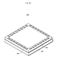
- FIG. 20 is a perspective view showing an overall structure of a solid-state imaging apparatus 302 according to the embodiment 3.
- the solid-state imaging apparatus 302 is made up of a solid-state imaging device 304 and a transparent protection plate 306.
- the solid-state imaging device 304 has a substantially square plate shape
- the transparent protection plate 306 has a substantially square plate shape that is one size smaller than the square of the solid-state imaging device 304.
- the solid-state imaging device 304 is a light-receiving chip produced by a semiconductor process and using a silicon substrate.
- a MOS-type image sensor chip is taken as an example of the solid-state imaging device 304. Note that the MOS-type image sensor chip is of a conventional type that is widely manufactured.
- the transparent protection plate 306 is made of synthetic resin having transparent characteristics.
- An example of the synthetic resin is acryl.
- the transparent protection plate 306 is not limited to acryl, and other materials may be used as long as they do not considerably change the optical characteristics of incident light and have transparent characteristics.
- the transparent protection plate 306 may be made of other synthetic resin, or glass.
- the transparent protection plate 306 is, on an upper surface thereof, provided with a plurality of terminal pads 308 (input-terminal pad or output terminal pad) for exchange of signals with external devices.
- the upper surface corresponds to amain surface of the transparent protection plate 306 that is opposite to another main surface that faces the solid-state imaging device 304.
- the terminal pads 308 are made of gold (Au).
- the terminal pads 308 may alternatively be made of aluminum (Al).
- FIG.21 is a perspective diagram showing an overall structure of the solid-state imaging device 304.
- a light-receiving portion 310 is formed in the center of the upper surface of the solid-state imaging device 304.
- the light-receiving portion 310 is provided with pixels (not illustrated) arranged two dimensionally, where each pixel is composed of a photodiode and a vertical switch (MOS-type transistor).
- MOS-type transistor MOS-type transistor
- a microlens is attached as a condenser (the microlens is not illustrated in the drawing).
- the solid-state imaging device 304 includes a vertical scanning circuit portion 309, a horizontal scanning circuit portion 311, a timing generating circuit portion 313, and so on in its periphery around the light-receiving portion 310. These circuit portions are hereinafter collectively referred to as "a peripheral circuit portion 315".
- the vertical scanning circuit portion 309 turns on the vertical switch that corresponds to one line, thereby transferring the line of charge from among the charge having been accumulated in the photodiodes, to the horizontal scanning circuit portion 311.
- the horizontal scanning circuit portion 311 has a horizontal shift resistor (not illustrated), and is operable to output the received charge to outside via later-stated electrodes 314, after performing horizontal transfer on pixels one by one. The stated operation is repeated for each line until completing transfer of all the lines of charges. As a result, one frame of pixel charges is outputted.
- the solid-state imaging device 304 is provided with a plurality of electrodes 314 on its periphery around the light-receiving portion 310, so as to apply input signal voltage required to operate the peripheral circuit portion 315 and to extract charges (output signal voltage) obtained by photoelectric conversion.
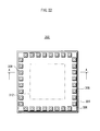
- FIG.22 is a plan view of the solid-state imaging apparatus 302
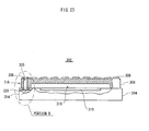
- FIG. 23 is a sectional viewof the solid-state imaging apparatus 302, which is cut at the line A.A.
- an area defined by a two-dot chain line corresponds to an area on which the light-receiving portion 310 is formed.
- the area is referred to as "light-receiving area 312".
- the terminal pads 308 correspond to the electrodes 314 (FIG.21) in one-to-one relation, in such a way that each terminal pad 308 is positioned immediately above a corresponding electrode 314. More specifically, each terminal pad 308 is placed in a position corresponding to a corresponding electrode 314 with the transparent protection plate 306 therebetween.
- each terminal pad 308 is arranged in a position (area) on the periphery (four sides) of the transparent protection plate 306 so that the terminal pad 308 will not prevent light from traveling onto the light-receiving area 312.
- the transparent protection plate 306 has a concave portion 316 so as to create a space between the light-receiving portion 310 and the transparent protection plate 306 in the direction vertical to thelight-receiving surface of the light-receiving portion 310 (the vertical direction corresponding to the direction in which the light travels).
- the purpose of forming the concave portion 316 is to enable the microlens to effectively exercise the light condensing function, by forming an air layer having a smaller index of refraction than that of the above-mentioned microlens.
- FIG. 24 shows an enlarged view of the portion B of FIG. 23, i.e. an enlarged view of the frame portion 318 and its periphery.
- the lower surface of the transparent protection plate 306 that opposes each terminal pad 308 is provided with conductive pads 320 that are in the same pattern formation as the terminal pads 308.
- Each conductive pad 320 is electrically connected to a corresponding one of the electrodes 314.
- holes 322 are provided with respect to the frame portion 318 so as to penetrate the transparent protection plate 306, for linking each terminal pad 308 with a corresponding conductive pad 320.
- a conductive foil 324 is attached to the side wall of each hole 322, to constitute a through hole 325 by means of a hole 322 and a conductive foil 324.
- An upper end of a conductive foil 324 is connected to a terminal pad 308, and a lower end thereof is connected to a conductive pad 320.
- an electrode 314 is to be electrically connected to a terminal pad 308 via a conductive member made of a conductive pad 320 and a conductive foil 324.
- An adhesive layer 326 attaches the lower surface of the frame portion 318 of the transparent protection plate 306 to the opposing surface (uppersurface) of the solid-state imaging device 304, thereby sealing the light-receiving portion 310 airtight.
- the transparent protection plate 306 whose main surface has substantially the same area as that of the main surface of the solid-state imaging device 304 is used to seal the light-receiving portion 310 airtight.
- terminal pads 308 electrically connected to the electrodes of the solid-state imaging device 304 are formed on one main surface of the transparent protection plate 306 that is opposite to another main surface to which the solid-state imaging device 304 is attached.
- the lengthwise/widthwise size of the solid-state imaging apparatus 302 is reduced substantially to the size of the solid-state imaging device 304 (sensor chip) .
- the thickness of the solid-state imaging apparatus 302 is able to be restrained substantially to a summation of the thickness of the solid-state imaging device 304 and the thickness of a transparent protection plate 306.
- the solid-state imaging apparatus 302 has a considerably smaller size than the size of conventional solid-state imaging apparatuses.
- the through hole 325 was explained to be constituted by attaching a conductive foil 324 to the side wall of a hole 322.
- a hole 322 is filled with a conductive material 332 to structure a through hole 334.
- a terminal pad 336 and a conductive pad 338 can have a perfect square shape.
- An example of the conductive material 332 is silver paint.
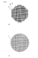
- FIG. 26A is a plan view showing an overview of a wafer 328 formed by orderly arranging solid-state imaging devices 304 in both the lengthwise and widthwise directions.
- the wafer 328 is of a conventional type widely manufactured, in which light-receiving portions 310, peripheral circuit portions 315, electrodes 314, and the like, are created, by a semiconductor process, on one main surface of a base substrate made of silicon.
- the wafer 328 is in condition for immediate dicing, where individual solid-state imaging devices 304 are still linked to each other.
- FIG.26B is a plan view showing an overall structure of a transparent protection plate linkage member 330 in which a plurality of transparent protection plates 306 are linked to each other on one plane.
- the arrangement of the transparent protection plates 306 corresponds to the arrangement of the solid-state imaging devices 304 on the wafer 328 explained above.
- a resin sheet (not illustrated) is prepared. After the resin sheet is heated to be softened, concave portions 316 (see FIG.23) are formed by press forming (Step P2). In press forming, a pair of dies made up of a upper die and a lower die is used. With respect to the lower die, convex portions each corresponding to the concave portions 316 are arranged both in the lengthwise and widthwise directions. The upper die has a flat surface. In the press forming, the softened resin sheet is subjected to pressure by being sandwiched between the upper and lower dies.
- Step P4 holes 322 (see FIG.24) are opened.
- punching may be performed using a set of a punch and dies.
- a sandblasting method may be used to open the holes 322.
- a protection plate is provided to be in contact with the upper surface of the resin sheet (the upper surface being a surface opposite to the surface provided with the concave portion), except for the positions at which the holes 322 are scheduled to be provided.
- Punching is specifically performed by blowing hard particles directed to the positions at which the holes 322 are scheduled to be provided.
- a plating method is used to attach a foil made of gold (Au) or aluminum (Al) to the resin sheet, thereby forming the conductive foils 324, the electrodes 314, and the conductive pads 320 (step P6).
- the foil of gold (Au) or aluminum (Al) attached on the masks as well as the masks is removed prior to moving onto the next step.
- the through holes 325 see FIG . 24
- the transparent protection plate linkage member 330 completes. Though not illustrated in FIG.26B, around the transparent protection plate linkage member 330, a remainder of the resin sheet exists as a continuation of the linkage member.
- An adhesive agent is applied to the lower surface (FIG.24) of the frame portion 318 (FIG.24) of the transparent protection plate linkage member 330, where the lower surface is at the side where the concave portion 316 is formed (Step P8). After this, the transparent protection plate linkage member 330 is superposed and pressed onto the wafer 328, so that the lower surface of the frame portion 318 be in contact with the wafer 328 (Step P12).
- the conductive pads 320 push away the adhesive agents to their vicinities, thereby contacting the conductive pads 320 and the electrodes 314.
- the adhesive agent may alternatively be applied onto the wafer 328 instead of onto the transparent protection plate linkage member 330. This is realized for example by the following concrete method.
- the transparent protection plate linkage member 330 is first superposed onto the wafer 328 so that each transparent protection plate 306 is superposed on a corresponding solid-state imaging device 304. Then in the area that faces the frame portion 318, an adhesive agent is applied by a screen printing method.
- the transparent protection plate linkage member 330 For attaching the transparent protection plate linkage member 330 to the wafer 328, it is possible to provide bumps between the conductive pads and corresponding electrodes 314. Furthermore, it is also possible to apply an adhesive agent to both of the transparent protection plate linkage member 330 and the wafer 328.
- Step P14 the wafer to which the transparent protection plate linkage member 330 has been attached is diced to respective pieces (Step P14), thereby completing each solid-state imaging apparatus 302 (as shown in FIG.20).
- a solid-state imaging apparatus has principally the same structure as the solid-state imaging apparatus 302 according to the embodiment 3, except for the manner of connection between the terminal pads and the conductive pads on a transparent protection plate. Accordingly, the structural elements that are the same as the structural elements of the embodiment 3 are assigned the same reference numbers, and explanation thereof is either omitted or restrained tominimum in the following description, so that the explanation of the connection manner is mainly focused.
- FIG.28 is a plan view of a solid-state imaging apparatus 350 according to the embodiment 4, and FIG. 29 is a cross sectional diagram of the solid-state imaging apparatus 350.of .FIG.28, which is cut at the line D ⁇ D.
- a plurality of terminal pads 354 are provided in areas of the upper surface of the transparent protection plate 352 that do not prevent light from traveling onto the light-receiving area 312 of the solid-state imaging device 304.
- the positions of the terminal pads 354 are the same as the positions of the terminal pads 308 (FIG.22) of the embodiment 3.
- FIG. 29 shows, in the lower surface of the frame portion 356 of the transparent protection plate 352, and at a position facing each terminal pad 354, a corresponding conductive pad 358 connected to an electrode 314 is formed.
- the conductive pads 358 have the same shape as the shape of the terminal pads 354.
- FIG. 30 is a diagram showing a sectional view of the transparent protection plate 352 at a position where a terminal pad 354 and a conductive pad 358 are formed.
- a conductive foil 360 being a conductive member, is formed from one main surface to the other main surface via a side surface of the transparent protection plate 352.
- One end of the conductive foil 360 is connected to the terminal pad 354, and the other end of the conductive foil 360 is connected to the conductive pad 358.
- the conductive foil 360 is made of gold (Au) or aluminum (A1), for example, and may be formed in a plating method.
- FIG. 31 is a perspective diagram of the part of the print wiring board 370 to which the solid-state imaging apparatus 302 (350) is to be mounted.
- the print wiring board 370 has lands 372 whose arrangement is the same as the arrangement of the terminal pads 308 (354) of the solid-state imaging apparatus 302 (350) .
- Theprintwiring board 370 is provided with a rectangular window 374 inside of the lands 372.
- the solid-state imaging apparatus 302 (350) is mounted to the print wiring board 370, by means of a flip chip mounting by which the lands 372 are directly connected to the terminal pads 308 (354) via the bumps (not illustrated).
- the ACF (anisotropic conductive foil) mounting method may also be adopted, where the ACF mounting method uses ACF and is one kind of the flip chip mounting.
- a camera lens (not illustrated) is provided at the front (left side in the paper in which the drawing is drawn) of the solid-state imaging apparatus 302 (350) to which the print wiring board 370 has been attached.
- the light from the camera lens passes through the window 374 to be incident onto the solid-state imaging apparatus 302 (350), so that photographing be performed.
- the required mounting space (lengthwise/widthwise size) of the solid-state imaging apparatus 302 (350) to the print wiring board 370 is restrained substantially down to the size of the solid-state imaging device 304 (sensor chip).
- the solid-state imaging apparatus 302 (350) will have a height that is restrained substantially down to the summation of the thickness of the solid-state imaging device 304 and the thickness of the transparent protection plate 306 (352). As a result, the solid-state imaging apparatus 302 (350) is able to contribute to further size reduction of imaging apparatuses, compared to cases where conventional solid-state imaging apparatuses are used.
- a corresponding imaging apparatus is able to have a size smaller in the optical-axis direction of the camera lens, meaning that the imaging apparatus is more slim than conventional imaging apparatuses.
- the reason is as follows.
- a print wiring board should be positioned outside the focus distance of the camera lens (i.e. the focus distance is between the camera lens and the light-receiving surface of the solid-state imaging device).
- the print wiring board is able to be positioned within the focus distance of the camera lens.
- the effect of making more slim imaging apparatuses would be more distinguished when the solid-state imaging apparatus 302 (350) is adopted for a camera-included mobile telephone that inherently has a substantial thickness in the optical-axis direction of the camera lens.
- the solid-state imaging apparatus 302 (350) has an improved positional accuracy between the light-receiving surface of the solid-state imaging device and the camera lens, compared to the conventional solid-state imaging apparatus 200 of FIG. 2.
- the reason is as follows. In both of the solid-state imaging apparatuses, positional alignment between the camera lens and the solid-state imaging apparatus is performed using the print wiring board as a reference.
- the conventional solid-state imaging apparatus 200 two components (i.e. a base portion 210 and a lead frame 240) are interposed between the CCD chip (solid-state imaging device) 230 and the print wiring board.
- the positional accuracy is affected by accumulation of variations caused in manufacturing the two components and variations caused in mounting the components.
- the solid-state imaging apparatus 302 (350) of the present embodiment only one component, namely a transparent protection plate 306 (352) will be interposed between the solid-state imaging device 304 and the print wiring board. Accordingly, in the solid-state imaging apparatus 302 (350), there will be smaller accumulation of such variations compared to the case of the conventional solid-state imaging apparatus 200.
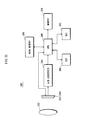
- FIG.32 is a block diagram showing an overall structure of a digital camera 380 that adopts the solid-state imaging apparatus 302 (350).
- the camera lens 382 forms an image of an object on the light-receiving surface of the light-receiving portion 310 of the solid-state imaging apparatus 302 (350).
- the solid-state imaging apparatus 302 (350) performs photoelectric conversion on the formed image pixel by pixel, and outputs charges to an A/D converter 384, pixel by pixel.
- the A/D converter 384 converts charges inputted from the solid-state imaging apparatus 302 (350) pixel by pixel, and outputs converted charges to the DSP (digital signal processor) 388 via a CPU 386.
- the DSP 388 performs image processing (e.g.
- the CPU 386 temporarily stores received digital images in a work memory 390.
- the digital images stored in the work memory 390 undergoes compression by means of a DCT (Discrete Cosine Transform) chip 392, and is stored thereafter in a recording memory 394. Note that the CPU 386 exercises comprehensive control over the entire system (see FIG.32).
- DCT Discrete Cosine Transform
- the present invention is applicable to imaging apparatuses such as a home video camera, a digital still camera, and a camera-included mobile telephone.
- the present invention offers a solid-state imaging apparatus having reduced area, volume, and weight, which contributes to reduction of size and weight of cameras.
- the present invention offers a solid-state imaging apparatus having much more excellent productivity compared to the conventional cases, which contributes to price reduction of cameras.
- the present invention is of extremely high value in terms of industrial applicability. Not only limited to home use cameras, the present invention is also applicable to any type of cameras.
- the light-receiving area is explained to be provided with light-receiving cells arranged two dimensionally.
- the present invention is also applicable to a line sensor and the like, in which light-receiving cells are arranged one dimensionally.
Landscapes
- Engineering & Computer Science (AREA)
- Multimedia (AREA)
- Signal Processing (AREA)
- Solid State Image Pick-Up Elements (AREA)
- Transforming Light Signals Into Electric Signals (AREA)
Abstract
Description
- The present invention relates to a solid-state imaging apparatus, and particularly relates to a technology of reducing the size of an imaging apparatus and of improving productivity of such imaging apparatuses.
- Recently, various imaging apparatuses such as a home video camera and a digital still camera have been commercially available.
Some types of such imaging apparatuses are equipped with a solid-state imaging apparatus.
Japanese Laid-open patent application No. H7-086544 (hereinafter, Patent Reference 1) and Japanese Laid-open Patent ApplicationNo. H10-313070 (hereinafter, PatentReference2) disclose such conventional solid-state imaging apparatuses. - FIG.1A is a plan view showing an overview of a conventional solid-
state imaging apparatus 100 disclosed in thePatent Reference 1. - FIG.1B is a diagram showing a cross sectional view of the solid-
state imaging apparatus 100 of FIG.1A, which is cut at the line of A-A'. - The
CCD chip 110 is shaped as a square. Eight input/output terminal pads 111 are provided along each of the right hand side and the left hand side of the square of theCCD chip 110. Underneath each of the input/output terminal pads 111, abump 112 having a height of about 10µm is provided.
Theglass substrate 120 is in a rectangular shape which is larger than theCCD chip 110. Sixteen electrode pads 121 (8 on the right hand side and 8 on the left hand side) are provided on theglass substrate 120, in position corresponding to thebumps 112 of theCCD chip 110 . Sixteenwirings 122 are formed on the upper surface of theglass substrate 120. - One end of each of the wirings is collected to the right hand side of the
glass substrate 120, and the other end the wiring is connected to acorresponding electrode pad 121.
For the purpose of moisture resistance and the like, a sealingmaterial 140 made of resin is formed on theglass substrate 120 in position corresponding to the contour of theCCD chip 110.
FIG.2A is a plan view showing an overview of a conventional solid-state imaging apparatus 200 disclosed in the Patent Reference 2. - FIG.2B is a diagram showing a cross sectional view of the solid-
state imaging apparatus 200 of FIG.2A, which is cut at the line of A-A'.
As FIG. 2A and FIG. 2B show, the conventional solid-state imaging apparatus 200 has the following structure. Achip bonding portion 211 is created as a concave groove, at the center of a base portion 210 (made of molded resin) of the solid-state imaging apparatus 200. To thechip bonding portion 211, aCCD chip 230 is attached via asilver paste 220. A bonding pad on theCCD chip 230 is connected tolead frames 240 viabonding wires 250. Furthermore, asealing glass 270 is attached to thebase portion 210 via apotting resin layer 260, so as to seal theCCD chip 230 together with thebonding wires 250 airtight. - Patent Reference 1: Japanese Laid-open Patent application No. H7-086544
- Patent Reference 2: Japanese Laid-open Patent Application No. H10-313070
- In the conventional solid-
state imaging apparatus 100 disclosed in thePatent Reference 1, theglass substrate 120 is substantially larger, in area, than theCCD chip 110.
This is because theglass substrate 120 has to have a part thereof to connect to an external device, at the surface thereof that faces towards theCCD chip 110 but does not overlap with theCCD chip 110 in position.
As a result, in thePatent Reference 1, the area of theglass substrate 120 is the major factor defining the area of the entire solid-state imaging apparatus 100, and so the area of the solid-state imaging apparatus is inherently larger than the area of theCCD chip 110. - In addition, in the solid-
state imaging apparatus 200 of the Patent Reference 2, thebase portion 210 and thesealing glass 270 are respectively larger, in area, than theCCD chip 230.
Therefore, the exterior size of thebase portion 210 or thesealing glass 270 is the major factor defining the exterior size of the entire solid-state imaging apparatus 200, and so the exterior size of the solid-state imaging apparatus 200 will be substantially larger than the exterior size of theCCD chip 230. - Meanwhile, it is strongly demanded to reduce the size and the weight of imaging apparatuses. Particularly for a camera-included portable telephone, reduction in size and weight of imaging apparatuses is a compelling problem. Even a small difference in size and weight of an imaging apparatus would largely affect the sales of the camera-included portable telephone. So as to minimize the difference in size and weight with portable cameras that do not include a camera, it is strongly desired to reduce the size and the weight of solid-state imaging apparatuses in the field of camera-included portable telephone.
In view of the described problems, the first object of the present invention is to reduce the size and the weight of the whole of a solid-state imaging apparatus, and further to contribute to reduction of size and weight of a camera to which the solid-state imaging apparatus is mounted, by reducing the area of a transparent protection plate such as a glass substrate, down to the area of a light-receiving chip or smaller, and by realizing a light-receiving chip that does not require a base portion through which mounting to an external device is performed. - Here, in the solid-
state imaging apparatus 100 of thePatent Reference 1, the area of theglass substrate 120 is clearly larger than the area of theCCD chip 110, and so attaching of theCCD chip 110 to theglass substrate 120 is performed after cutting a wafer into chips.
In thesolid-state imaging apparatus 200 of the Patent Reference 2, it is required to perform, after production of a wafer and cutting the wafer into chips, many steps to each chip such as a die bonding step, a wire bonding step, a potting resin layer application step, a seal glass attaching step, a potting resin layer hardening step, and a lead frame forming step, which degrades productivity. - In addition, in the solid-
state imaging apparatus 200 of the Patent Reference 2, the distance between thesealing glass 270 and theCCD chip 230 is defined by the thickness of thepotting resin layer 260, and so tends to have variations, which makes production difficult.
In view of this, the second object of the present invention is to provide a solid-state imaging apparatus having excellent productivity, and a manufacturing method of such a solid-state imaging apparatus having excellent productivity, so as to realize cost reduction of a solid-state imaging apparatus, and further to realize cost reduction of a camera to which the solid-state imaging apparatus is mounted. - So as to achieve the above-stated objects, a solid-state imaging apparatus according to the present invention is a solid-state imaging apparatus having: a light-receiving chip having a plurality of light-receiving cells arranged either one dimensionally or two dimensionally on one main surface of a base substrate; and a transparent protection plate attached to the main surface of the base substrate to cover the light-receiving cells, a space being formed between the light-receiving cells and the transparent protection plate, where an area of the transparent protection plate is equal to or smaller than an area of the light-receiving chip.
- So as to achieve the above-stated objects, a camera of the present invention has a solid-state imaging apparatus according to the present invention.
So as to achieve the above-stated objects, a light-receiving chip according to the present invention is a light-receiving chip having: a plurality of light-receiving cells arranged either one dimensionally or two dimensionally on a first main surface of a base substrate; a plurality of input/output lines provided on the first main surface of the base substrate; a plurality of electrodes for connecting to outside devices, the electrodes being formed on a second main surface of the base substrate that is opposite to the first main surface; and a plurality of conductive units insulated from each other, each conductive unit electrically connecting one of the input/output lines with a corresponding one of the electrodes. - So as to achieve the above-stated objects, a manufacturing method of solid-state imaging apparatus according to the present invention is amanufacturingmethodof solid-state imaging apparatuses each having: a light-receiving chip provided with a set of light-receiving cells arranged either one dimensionally or two dimensionally on one main surface of a base substrate; and a transparent protection plate, the manufacturing method including: a protection-plate preparing step of preparing a plurality of transparent protection plates each having an area that is equal to or smaller than an area of the light-receiving chip; an attaching step of attaching the prepared transparent protection plates onto a semiconductor wafer of light-receiving chips so that each set of light-receiving cells is covered by a corresponding one of the transparent protection plates, thereby generating an attached member in which the transparent protection plates are attached to the light-receiving chips; and a cutting step of cutting the attached member generated in the attaching step into respective solid-state imaging apparatuses.
- In the above-stated solid-state imaging apparatus and the above-stated camera, the area of a solid-state imaging apparatus is not larger than the area of a light-receiving chip. According to this characteristic, in a manufacturing process, it becomes possible to attach transparent protection plates to a wafer, and to thereafter cut them together into respective chips. The productivity of such a manufacturing process is much better than that of the conventional processes.
In addition, the index of refraction in a space formed between a light-receiving cell and a corresponding transparent protection plate is smaller than the index of refraction of a collective lens normally provided on the light-receiving cell. Therefore, formation of the space enables favorable light-collective characteristics. [0016]Accordingly, it becomes possible to reduce the price of a solid-state imaging apparatus, which further contributes to price reduction of a camera.
In addition, in the solid-state imaging apparatus and the camera, the light-receiving chip further has: a plurality of input/output lines provided on the main surface of the base substrate on which the light-receiving cells are arranged, the main surface being a first main surf ace; a plurality of electrodes for connecting to outside devices, the electrodes being provided on a second main surface of the base substrate that is opposite to the first main surface; and a plurality of conductive units insulated from each other, each conductive unit electrically connecting one of the input/output lines with a corresponding one of the electrodes. - According to the solid-state imaging apparatus, the camera, and the light-receiving chip, the electrodes for outside connection are provided on the second main surface that is different from the first main surface. Accordingly, it becomes possible to reduce the area of a transparent protection plate to be equal to or smaller than the area of a light-receiving chip.
This further leads to reduction of size and weight of an entire solid-state imaging apparatus, which contributes to reduction of size and weight of a camera. - In addition, for example, for a conventional type that seals a bonding wire airtight, the distance between a surface of a light-receiving chip and a transparent protection plate should be at least about the height of the bonding wire, so as to prevent the bonding wire from interfering with the light-receiving chip or with the transparent protection plate. However, the stated structure does not require a bonding wire, and that the distance may be equal to or smaller than the height of a bondingwire, which enables the thickness of a solid-state imaging apparatus to be thinner than conventionally. This creates a multiplier effect with the area reduction effect stated above, in reducing the size of a camera.
- In addition, in the solid-state imaging apparatus, the camera, and the light-receiving chip, each of the conductive units is a through hole provided through the base substrate.
According to the stated structures, a through hole is generated instead of a conventional bonding pad. Therefore, the designing is performed without any regard to the conventional designing rule that depends on the accuracy of a wire bonding apparatus, and the like. - As a result, it becomes possible to have expectations that the area of the light-receiving chip be reduced because the structures allow greater layout flexibility, which contributes to reduction in size and weight of a camera.
Moreover, provision of a plurality of through holes is performed onto a wafer, which is a manufacturing advantage.
In addition, in the solid-state imaging apparatus, the camera, and the light-receiving chip, each of the electrodes is provided on an opening of a corresponding through hole on the second main surface. - According to the stated structures, no wiring pattern is required on the second main surface. Therefore the manufacturing process becomes simpler and the effect of reducing the manufacturing cost can be expected.
In addition, in the solid-state imaging apparatus, the camera, and the light-receiving chip, each of the conductive units is a wiring formed on a side surface of the base substrate.
According to the stated structure, a wiring pattern is provided for a side surface, instead of provision of a conventional bonding pad. Therefore the entire area of a bonding pad becomes unnecessary. Therefore, the designing is performed without any regard to the conventional designing rule that depends on the accuracy of a wire bonding apparatus, and the like. - Accordingly, it is possible to have expectations that the area of the light-receiving chip be reduced because the structures allow greater layout flexibility, which contributes to reduction in size and weight of a camera.
In addition, in the solid- state imaging apparatus and the camera, the light-receiving chip further has: a plurality of input/output lines provided on the main surface of the base substrate on which the light-receiving cells are arranged, the main surface being a firstmainsurface; a plurality of electrodes for connecting to outside devices, the electrodes being formed on a second main surface of the base substrate that is opposite to the first main surface; and a plurality of conductive units insulated from each other, each conductive unit electrically connecting one of the input/output lines with a corresponding one of the electrodes; and a plurality of collective lenses provided on a light-receiving of the onemain surface of the base substrate, where the space is formed between the collective lenses and the transparent protection plate, and an index of refraction of the space is smaller than an index of refraction of the collective lenses. - According to the stated structures, the electrodes for outside connection are provided on the second main surface that is different from the first main surface (the first main surface being the light-receiving surface for the light-receiving chip). Therefore, the area of a transparent protection plate is able to be reduced to equal to or smaller than the area of a light-receiving chip.
Therefore, the entire solid-state imaging apparatus is able to be reduced in size and weight, which contributes to reduction in size and weight of a camera. - In addition, on the side of the light-receiving surface, there is no conjunction part such as a bump, and no protrusion such as a wire bonding. Therefore, it becomes possible to reduce the space formed between a collective lens and a transparent protection plate.
In addition, in the solid-state imaging apparatus and the camera, the solid-state imaging apparatus further has: a sealing material operable to fix the base substrate and the transparent protection plate, where the first main surface is made up of the light-receiving area on which the light-receiving cells are arranged and a periphery area surrounding the light-receiving area, the sealing material being provided on the periphery area, and the space is sealed airtight by means of the base substrate, the transparent protection plate, and the sealing material. - According to the stated structures, the light-receiving area is sealed airtight, and so is prevented from dust or from corrosion.
In addition, in the solid-state imaging apparatus and the camera, the main surface is made up of a light-receiving area on which the light-receiving cells are arranged and a periphery area surrounding the light-receiving area, the transparent protection plate has a skirt portion at a periphery thereof, and the skirt portion is attached onto the periphery area of the main surface, thereby sealing the light-receiving cells airtight and forming the space between the light-receiving cells and the transparent protection plate. - According to the stated structures, the distance between the light-receiving area and the transparent protection plate depends on the accuracy of the form of the transparent protection plate. Therefore, the distance hardly varies, which contributes to productivity improvement.
In addition, in the solid-state imaging apparatus and the camera, the skirt portion is formed by plating metal on the periphery of the transparent protection plate that is a flat plate made of glass or resin. - In addition, in the solid-state imaging apparatus and the camera, the transparent protection plate is a flat plate made of resin, and the skirt portion is formed by pressing the flat resin plate.
According to the stated structures, manufacturing enables the distance between the light-receiving area and the transparent protection plate to be in the accuracy of about several µm.
In addition, in the solid-state imaging apparatus and the camera, the main surface is made up of a light-receiving area on which the light-receiving cells are arranged and a periphery area surrounding the light-receiving area, the light-receiving chip has, on the periphery area of the main surface, a rib portion having a loop shape, the rib portion is attached onto a periphery of the transparent protection plate, thereby sealing the light-receiving cells airtight and forming the space between the light-receiving cells and the transparent protection plate. - According to the stated structures, the distance between the light-receiving area and the transparent protection plate depends on the accuracy of the form of the light-receiving chip. Therefore, the distance hardly varies, which contributes to productivity improvement.
In addition, in the solid-state imaging apparatus and the camera, the rib portion is an insulator made of a material for protective foil. - According to the stated structures, manufacturing enables the distance between the light-receiving area and the transparent protection plate to be in the accuracy of about several µm.
Furthermore, rib-portion forming is performed in the diffusion process that is prior to the chip-cutting process, and so no extra process is required for the rib-portion forming, which contributes to productivity improvement.
In addition, in the solid-state imaging apparatus and the camera, being manufactured by attaching transparent protection plates onto a semiconductor wafer of light-receiving chips to generate an attached member in which the transparent protection plates are attached to the light-receiving chips respectively, and cutting the attached member into respective solid-state imaging apparatuses. - According to the stated structures, the transparent protection plates are attached to the wafer, and then the resulting attached member is cut into respective chips, which contributes to great productivity improvement compared to conventional cases.
Accordingly, it becomes possible to reduce the price of a solid-state imaging apparatus, which further contributes to price reduction of a camera. - In addition, in the solid-state imaging apparatus and the camera, being manufactured by simultaneously cutting out the light-receiving chip and the transparent protection plate, as a set.
According to the stated structure, only one process is required for cutting out a set of light-receiving chip and transparent protection plate. This is a reduction in number of processes, and also enables to easily obtain a clean cross section for a set of light-receiving chip and transparent protection plate.
In addition, in the solid-state imaging apparatus and the camera, the main surface has a light-receiving area in a central portion thereof, and a plurality of electrodes outside the light-receiving area, the transparent protection plate includes: a plurality of terminal pads formed on the other main surface that is different from the main surface; and a plurality of conductive members insulated from each other, each conductive member electrically connecting one of the electrodes with a corresponding one of the terminal pads. - According to the stated structures, it becomes possible to restrain the lengthwise/widthwise size of an entire solid-state imaging apparatus down to the lengthwise/widthwise size of a corresponding solid-state imaging device. In addition, the thickness of an entire solid-state imaging apparatus is also restrained down to substantially the summation of the thickness of the solid-state imaging device and the thickness of a corresponding transparent protection plate. As a result, the solid-state imaging apparatus will be much smaller, in size, than conventional solid-state imaging apparatuses.
In addition, in the solid-state imaging apparatus and the camera, a plurality of holes are provided through the transparent protection plate, the holes being provided in position that will not prevent light from traveling onto the light-receiving area, and part of each of the conductive members is positioned in a corresponding one of the holes. - In addition, in the solid-state imaging apparatus and the camera, the part of each of the conductive members that is positioned in the corresponding hole is a conductive foil attached to a side wall of the of the corresponding hole.
In addition, in the solid-state imaging apparatus and the camera, the part of each of the conductive members that is positioned in the corresponding hole is a conductive material filling the corresponding hole.
According to the stated structures, a hole is generated instead of a conventional bonding pad. Therefore, the designing is performed without any regard to the conventional designing rule that depends on the accuracy of a wire bonding apparatus, and the like. - As a result, it becomes possible to have expectations that the area of the light-receiving chip be reduced because the structures allow greater layout flexibility, which contributes to reduction in size and weight of a camera.
Furthermore, holes are provided for a sheet, which is a manufacturing advantage.
In addition, in the solid-state imaging apparatus and the camera, each of the conductive members is a conductive foil attached to the main surface, a side surface, and the other main surface of the transparent protection plate. - According to the stated structures, a conductive foil is provided on a side surface, instead of provision of a conventional bonding pad. Therefore the entire area of a bonding pad becomes unnecessary. Therefore, the designing is performed without any regard to the conventional designing rule that depends on the accuracy of a wire bonding apparatus, and the like.
Accordingly, it is possible to have expectations that the area of the light-receiving chip be reduced because the structures allow greater layout flexibility, which contributes to reduction in size and weight of a camera. - In addition, a camera according to the present invention is a solid-state imaging apparatus of
Claim 1; and a print wiring board having lands arranged to correspond, in position, to terminals of the solid-state imaging apparatus, where each of the terminals is flip-chip mounted directly to a corresponding one of the lands.
According to the stated structure, the thickness of a solid-state imaging apparatus is able to be restrained to substantially the summation of the thickness of a solid-state imaging device and the thickness of a transparent protection plate. - According to the manufacturing method of a solid-state imaging apparatus, the transparent protection plates are attached to the wafer, and then the resulting attached member is cut into respective chips, which contributes to great productivity improvement compared to conventional cases.
Accordingly, it becomes possible to reduce the price of a solid-state imaging apparatus, which further contributes to price reduction of a camera. - In addition, in the manufacturing method, for one solid-state imaging apparatus, a corresponding main surface is made up of a light-receiving area on which a set of light-receiving cells are arranged and a periphery area surrounding the light-receiving area, each of the transparent protection plates prepared in the protection-plate preparing step has a skirt portion at a periphery of the transparent protection plate, and in the attaching step, a corresponding set of light-receiving cells of a solid-state imaging apparatus is sealed airtight by a skirt portion of a corresponding transparent protection plate that is attached onto a corresponding periphery area, so as to form a space between the set of light-receiving cells and the transparent protection plate.
- According to the stated structure, the distance between the light-receiving area and the transparent protection plate depends on the accuracy of the form of the light-receiving chip. Therefore, the distance hardly varies, which contributes to productivity improvement.
In addition, in the manufacturing method, each of the transparent protection plates is a flat plate made of glass or resin, and in the protection-plate preparing step, a corresponding skirt portion is created by plating metal on the periphery of each of the transparent protection plates. - In addition, in the manufacturing method, each of the transparent protection plates is a flat plate made of resin, and in the protection-plate preparing step, a corresponding skirt portion is created by pressing the flat resin plate.
According to the stated structures, manufacturing enables the distance between the light-receiving area and the transparent protection plate to be in the accuracy of about several µm.
In addition, in the manufacturing method, a wafer preparing step of preparing the semiconductor wafer of light-receiving chips, so that each light-receiving chip has a rib portion in a loop shape, where for each one solid-state imaging apparatus, a corresponding main surface is made up of a light-receiving area on which a set of light-receiving cells are arranged and a periphery area surrounding the light-receiving area, a rib portion being provided in the periphery area, and in the attaching step, the set of light-receiving cells is sealed airtight and a space is formed between the set of light-receiving cells and a corresponding transparent protection plate, as a result of a periphery of the transparent protection plate positioned on the rib portion. - According to the stated structure, the distance between the light-receiving area and the transparent protection plate depends on the accuracy of the form of the light-receiving chip. Therefore, the distance hardly varies, which contributes to productivity improvement.
In addition, in the manufacturing method, in the wafer preparing step, a rib portion of a corresponding light-receiving chip is made of an insulative material that is the same as a material of a protection foil.
According to the stated structure, manufacturing enables the distance between the light-receiving area and the transparent protection plate to be in the accuracy of about several µm. - Furthermore, rib-portion forming is performed in the diffusion process that is prior to the chip-cutting process, and so no extra process is required for the rib-portion forming, which contributes to productivity improvement.
In addition, in the manufacturing method, in the protection-plate preparing step, a sheet in which the plurality of transparent protection plates are linked together is prepared, in the attaching step, the sheet of the transparent protection plates is attached onto the plurality of light-receiving chips in the state of the semiconductor wafer, and in the cutting step, a light-receiving chip and a corresponding transparent protection plate is cut out as a set simultaneously. - According to the stated structure, only one process is required for cutting out a set of light-receiving chip and transparent protection plate. This is a reduction in number of processes, and also enables to easily obtain a clean cross section for a set of light-receiving chip and transparent protection plate.
- FIG.1A is a plan view showing an overview of a conventional solid-
state imaging apparatus 100 disclosed in thePatent Reference 1. - FIG.1B is a diagram showing a cross sectional view of the solid-
state imaging apparatus 100 of FIG.1A, which is cut at the line of A-A'. - FIG.2A is a plan view showing an overview of a conventional solid-
state imaging apparatus 200 disclosed in the Patent Reference 2. - FIG.2B is a diagram showing a cross sectional view of the solid-
state imaging apparatus 200 of FIG.2A, which is cut at the line of A-A'. - FIG.3A is a plan view showing a solid-
state imaging apparatus 10 according to theembodiment 1 of the present invention. - FIG . 3B is a diagram showing a sectional diagramof the solid-
sate imaging apparatus 10, which is cut at the line A-A' of FIG.3A. - FIG. 4A is a diagram showing a sectional view of a
transparent protection plate 12 that results by forming-,-using a plating method, a skirt portion (metal 12b) to a periphery portion of aflat plate 12a made of glass or acrylic resin, and the like. As shown in this drawing, the periphery portion of thetransparent protection plate 12 is thicker than the central portion thereof by "thickness ofcollective lens 16 +α". - FIG.4B is a diagram showing a sectional view of a
transparent protection plate 12 that results by forming a skirt portion by subjecting acrylic resin and the like to press forming, so that the periphery portion of thetransparent protection plate 12 is thicker than the central portion thereof by "thickness ofcollective lens 16 +α". - FIG. 5 is a diagram showing a sectional view of the solid-
state imaging device 11 in the vicinity of one of the through holes 17. - FIG. 6A is a plan view showing a solid-
state imaging apparatus 30 according to the modification example 1 of the present invention. - FIG. 6B is a diagram showing a sectional view of the solid-
state imaging apparatus 30 which is cut at the line A-A' of FIG.6A. - FIG.7 is a diagram showing a detailed sectional view of the solid-
state imaging device 31 in the vicinity of one of the throughholes 17, according to the modification example 1 of the present invention. - FIG.8A is a plan view showing a solid-
state imaging apparatus 40 according to the modification example 2 of the present invention. - FIG.8B is a diagram showing a sectional view of the solid-
state imaging apparatus 40 which is cut at the line A-A' of FIG.8A. - FIG.9 is a diagram showing a detailed sectional view of the solid-
state imaging device 41 in the vicinity of one of theconductive wires 45, according to the modification example 2 of the present invention. - FIG.10 is a diagram showing an overview of a manufacturing method of a solid-
state imaging apparatus 10, in the case where the skirt portion of thetransparent protection plate 12 is formed by a plating method (see FIG.4A). - FIG.11A is a diagram showing a sheet of solid-
state imaging device 11, which is generated by Steps S1-S5 of themanufacturing method 1. - FIG.11B is a diagram showing a sheet of
transparent protection plate 12, which is generated by Step S6 of themanufacturing method 1. - FIG.12 is a diagram showing an overview of a manufacturing method of a solid-
state imaging apparatus 10, in the case where the skirt portion of thetransparent protection plate 12 is formed by subjecting acrylic resin and the like to press forming (See FIG. 4B). - FIG.13A is a diagram showing a sheet of solid-
state imaging device 11 generated in Steps S11-S15 of the manufacturing method 2. - FIG.13B is a diagram showing a sheet of
transparent protection sheet 12 generated in Step S16 of the manufacturing method 2. - FIG.14 is a diagram showing an overview of a manufacturing method of a solid-
state imaging apparatus 10, in the case where the rib portion of the solid-state imaging device 11 is formed in the diffusion process. - FIG.15A is a diagram showing the sheet of solid-
state imaging device 11 generated in Steps S21-25 of the manufacturing method 3. - FIG 15B is a diagram showing a sheet of
transparent protection plate 12 generated in Step S26 of the manufacturing method 3. - FIG. 16A is a plan view showing a solid-
state imaging apparatus 60 according to the embodiment 2 of the present invention. - FIG .16B is a diagram showing a sectional-view of the solid-
state imaging apparatus 60, which is cut at the line A-A' of FIG.16A. - FIG.17 is a diagram showing an overview of a manufacturing method of a solid-
state imaging apparatus 60, in the case where the skirt portion of thetransparent protection plate 62 is formed by a plating method. - FIG.18 is a diagram showing an overview of a manufacturing method of a solid-
state imaging apparatus 60, in the case where the skirt portion of thetransparent protection plate 62 is formed by subjecting acrylic resin and the like to press forming. - FIG.19 is a diagram showing an overview of a manufacturing method of a solid-
state imaging apparatus 60, in the case where the rib portion of the solid-state imaging device 61 is formed in the diffusion process. - FIG.20 is a perspective view showing an overall structure of a solid-
state imaging apparatus 302 according to the embodiment 3. - FIG. 21 is a perspective diagram showing an overall structure of the solid-
state imaging device 304. - FIG.22 is a plan view of the solid-
state imaging apparatus 302. - FIG. 23 is a sectional view of the solid-
state imaging apparatus 302, which is cut at the line A.A. - FIG.24 shows an enlarged view of the portion B of FIG.23, i.e. an enlarged view of the
frame portion 318 and its periphery. - FIGs.25A and 25B are respectively a diagram showing a modification example of the embodiment 3. FIG.25A is a part of the plan view of the transparent protection plate 6, and FIG.25B is a cross sectional view of the transparent protection plate 6 cut at the line C.C.
- FIG.26A is a plan view showing an overview of a
wafer 328 formed by orderly arranging solid-state imaging devices 304 in both the lengthwise and widthwise directions. - FIG.26B is a plan view showing an overall structure of a transparent protection
plate linkage member 330 in which a plurality oftransparent protection plates 306 are linked to each other on one plane. - FIG.27 is a diagram showing a manufacturing method of the solid-state imaging device 4.
- FIG.28 is a plan view of a solid-
state imaging apparatus 350 according to the embodiment 4. - FIG. 29 is a cross sectional diagram of the solid-
state imaging apparatus 350 of FIG.28, which is cut at the line D.D. - FIG. 30 is a diagram showing a sectional view of the
transparent protection plate 352 at a position where aterminal pad 354 and aconductive pad 358 are formed. - FIG. 31 is a perspective diagram of the part of the
print wiring board 370 that is to be mounted in the solid-state imaging apparatus 302 (350). - FIG.32 is a block diagram showing an overall structure of a
digital camera 380 that adopts the solid-state imaging apparatus 302 (350). -
- 10
- solid-state imaging apparatus'
- 11
- solid-state imaging device
- 11a
- insulation material
- 12
- transparent protection plate
- 12a
- flat plate
- 12b
- metal
- 12c
- skirt portion
- 13
- sealing material
- 14
- base substrate
- 15
- electrode
- 16
- collective lens
- 17
- through hole
- 18
- light-receiving area
- 19
- periphery area
- 20
- space
- 21
- hole
- 22
- insulation material
- 23
- input/output line
- 24
- contact portion
- 25
- conductive member
- 26
- pad
- 27
- filling material
- 30
- solid-state imaging apparatus
- 31
- solid-state imaging device
- 32
- electrode
- 33
- conductive member
- 40
- solid-state imaging apparatus
- 41
- solid-state imaging device
- 42
- base substrate
- 43
- electrode
- 44
- side surface
- 45
- conductive wire
- 46
- insulation material
- 47
- input/output line
- 48
- contact portion
- 49
- conductive member
- 50
- pad
- 60
- solid-state imaging apparatus
- 61
- solid-state imaging device
- 62
- transparent protection plate
- 63
- sealing material
- 64
- base substrate
- 65
- electrode
- 66
- collective lens
- 68
- light-receiving area
- 69
- periphery area
- 70
- space
- 302
- solid-state imaging apparatus
- 304
- solid-state imaging device
- 306
- transparent protection plate
- 308
- terminal pad
- 309
- vertical scanning circuit portion
- 310
- light-receiving portion
- 311
- horizontal scanning circuit portion
- 312
- light-receiving area
- 313
- timing generating circuit portion
- 314
- electrode
- 315
- peripheral circuit portion
- 316
- concave portion
- 318
- frame portion
- 320
- conductive pad
- 322
- hole
- 324
- conductive foil
- 325
- through hole
- 326
- adhesive layer
- 328
- wafer
- 330
- transparent protection plate linkage member
- 332
- conductive material
- 334
- through hole
- 336
- terminal pad
- 338
- conductive pad
- 350
- solid-state imaging apparatus
- 352
- transparent protection plate
- 354
- terminal pad
- 356
- frame portion
- 358
- conductive pad
- 360
- conductive foil
- 370
- print wiring board
- 372
- land
- 374
- window
- 380
- digital camera
- 382
- camera lens
- 384
- A/D converter
- 386
- CPU
- 388
- DSP
- 390
- work memory
- 392
- chip
- 394
- recording memory
- FIG.3A is a plan view showing a solid-
state imaging apparatus 10 according to theembodiment 1 of the present invention.
FIG. 3B is a diagram showing a sectional diagramof the solid-sate imaging apparatus 10, which is cut at the line A-A' of FIG.3A.
As FIGs.3A and 3B show, the solid-state imaging apparatus 10 of theembodiment 1 is made up of a solid-state imaging device 11, atransparent protection plate 12, and a sealingmaterial 13. - The solid-
state imaging device 11 is a light-receiving chip such as a CCD chip and a MOS chip, for example. The solid-state imaging device 11 includes abase substrate 14,electrodes 15,collective lenses 16, and throughholes 17.
The first main surface of thebase substrate 14 is divided into a light-receivingarea 18 and a periphery area 19 (the first main surface corresponds to the upper surface in FIG.3B, and is hereinafter referred to as "light-receiving surface"). The light-receivingarea 18 is provided with a plurality of light-receiving cells arranged either one dimensionally or two dimensionally, where each light-receiving cell corresponds to one pixel. Theperiphery area 19 is an area positioned around the periphery of the light-receiving area, into which circuits other than the light-receiving cells are integrated. In the present embodiment, light-receiving cells corresponding to 300,000 pixels are arranged two dimensionally in the light-receiving area: - On the light-receiving surface, a plurality of input/output lines are provided, including a power-source input line, input lines for various control signals, and an output line for an image signal.
Thebase substrate 14 is conventionally a semiconductor substrate made of silicon. Areas of thebase substrate 14 that are in contact with theelectrodes 15, the throughholes 17, the input/output lines, and the like are covered by an insulation material such as silicon oxide and silicon nitride. - The
electrodes 15 are formed on the second main surface of thebase substrate 14 in the vicinity of the throughholes 17 for outside connection. An example of anelectrode 15 is a bump. The second main surface is positioned at the back of the light-receiving surface (the lower surface in FIG.3B) and so is hereinafter referred to as "back surface". Theelectrodes 15 are used to connect to corresponding terminals of a circuit substrate in mounting the solid-state imaging apparatus 10 to the circuit substrate.
Each of thecollective lenses 16 is provided on the light-receivingarea 18, and functions to collect a projected image on the light-receivingarea 18 by means of a corresponding light-receiving cell. Thecollective lenses 16 enhance light-receiving sensitivity. - The through holes 17 are respectively a conductive member electrically connecting the light-receiving surface and the back surface. The through holes 17 are insulated one from another, and each insulated through
hole 17 connects a corresponding one of the input/output lines to a corresponding one of theelectrodes 15.
Here, the number of theelectrodes 15 and the number of the throughholes 17 are respectively equal to the number of the input/output lines provided on the light-receiving surface. In the present embodiment, there are twentyelectrodes 15, twenty throughholes 17, and twenty input/output lines. - The
transparent protection plate 12 is made of glass or acrylic resin, for example, which is able to transmit incident light without considerably changing the optical characteristics of the incident light. Thetransparent protection plate 12 is attached to the base substrate to entirely cover the light-receiving cells. Thetransparent protection plate 12 functions to protect the light-receivingarea 18 and thecollective lenses 16 of the solid-state imaging device 11 from physical damage and from dust. It should be noted here that the area of thetransparent protection plate 12 may be equal to or smaller than the area of the solid-state imaging device 11. In the present embodiment, thetransparent protection plate 12 and the solid-state imaging device 11 have substantially the equal area. - The sealing
material 13 fixes, at theperiphery area 19, thebase substrate 14 and thetransparent protection plate 12.
Here, thetransparent protection plate 12 has a periphery portion that is thick and is in a loop shape (hereinafter "skirt portion"). As a result, thetransparent protection plate 12 has such a concave shape that the part thereof covering the light-receivingarea 18 is recessed with respect to the part thereof corresponding to theperiphery area 19. The skirt portion of thetransparent protection plate 12 is attached to theperiphery area 19 by means of the sealingmaterial 13, thereby sealing the light-receiving cells airtight and forming aspace 20 between thecollective lenses 16 and thetransparent protection plate 12. Alternatively, the solid-state imaging device 11 may have a protrusion having a loop shape, in the periphery area 19 (the loop-shaped protrusion being hereinafter referred to as "rib portion"), so that theperiphery area 19 protrudes with respect to the light-receivingarea 18. In this case, the periphery of thetransparent protection plate 12 is attached to the rib portion of the solid-state imaging device 11 by means of the sealingmaterial 13, thereby sealing the light-receiving cells airtight and forming thespace 20 between thecollective lenses 16 and thetransparent protection plate 12. - Furthermore, the index of refraction of the
space 20 is smaller than the index of refraction of thecollective lens 16.
For example, when for example a resin material having an index of refraction of about 1.5 is adopted for thecollective lens 16, it is desirable that the index of refraction for thespace 20 is about 1.0. Here, thespace 20 is filled with air or inert gas. Alternatively thespace 20 may be in a vacuum state, in a sense that thespace 20 is under pressure lower than atmospheric pressure. - In addition, the
collective lenses 16 may be made of a material having an index of refraction of about 2.0 or more, and thespace 20 may be filled with resin having an index of refraction of about 1.5, for example.
In addition, the air with which thespace 20 is filled should desirably be dry air, and the inert gas is specifically helium, neon, argon, nitride, a mixture of them, and the like.
Regardingthespace20, the minimum size for the distance between thecollective lenses 16 and thetransparent protection plate 12 is "α" that only takes into account accuracy such as variation of components and production accuracy. As a result, the distance between thebase substrate 14 and thetransparent protection plate 12 will be "thickness ofcollective lens 16 +α" , which is equal to or smaller than the height of abonding wire, which would be required for preventing interference with a bonding wire in a conventional type that uses a bonding wire. Specifically, it is sufficient that "α" is several ten times of the accuracy such as variation of components and production accuracy. For example, when the accuracy is about several µm, then the value of "α" may be about several 10 µm - 100 µm. - The following explains a concrete example showing how to enable a distance between the
base substrate 14 and thetransparent protection plate 12 to be "thickness ofcollective lens 16 +α".
FIG. 4A is a diagram showing a sectional view of atransparent protection plate 12 that results by forming, using a plating method, a skirt portion (metal 12b) to a periphery portion of aflat plate 12a made of glass or acrylic resin, and the like. As shown in this drawing, the periphery portion of thetransparent protection plate 12 is thicker than the central portion thereof by "thickness ofcollective lens 16 +α". - FIG.4B is a diagram showing a sectional view of a
transparent protection plate 12 that results by forming a skirt portion by subjecting acrylic resin and the like to press forming, so that the periphery portion of thetransparent protection plate 12 is thicker than the central portion thereof by "thickness ofcollective lens 16 +α".
FIG.4C is a diagram showing a sectional view of a solid-state imaging device 11 whoseperiphery area 19 is provided with a rim portion, thereby causing the periphery portion of the solid-state imaging device 11 to be thicker than the central portion by "thickness ofcollective lens 16 +α". The rim portion is formed in the diffusion process, using aninsulation material 11a that is the same material as used for a protection foil such as a nitride foil and an oxide foil. - In the
transparent protection plates 12 respectively of FIGs . 4A and 4B, and in the solid-state imaging device 11 of FIG.4C, it is possible to enable a distance between the solid-state imaging device 11 and thetransparent protection plate 12 to be "thickness ofcollective lens 16 +α" , by fixing abase substrate 14 and atransparent protection plate 12 at theperiphery area 19 by means of the sealingmaterial 13. Note that any combination of the FIGs.4A-4C is also possible. It is also possible to make the distance shorter, by take into consideration the thickness of the sealingmaterial 13. Still further, it is also possible to generate "thickness ofcollective lens 16 +α" by means of only the thickness of the sealingmaterial 13. - An image formed by an image-forming lens (not illustrated) is projected onto the light-receiving
area 18 after being transmitted through thetransparent protection plate 12 and thespace 20. Then the projected image is collected by means of thecollective lenses 16 to be subjected to photoelectric conversion by means of each light-receiving cell. As a result, the solid-state imaging device 11 outputs an image signal.
FIG. 5 is a diagram showing a sectional view of the solid-state imaging device 11 in the vicinity of one of the through holes 17. - As FIG . 5 shows , a
hole 21 is provided through thebase substrate 14, and both main surfaces of thebase substrate 14 and the inside thehole 21 are coated with aninsulation material 22. Furthermore, the input/output line 23 provided up to the vicinity of thehole 21 on the light-receiving surface (upper surface of FIG.5) is electrically connected to theconductive member 25 at acontact portion 24. Theconductive member 25 is provided through thebase substrate 14 by penetrating through thehole 21 from the light-receiving surface to the back surface of the base substrate 14 (lower surface of FIG.5), to form apad 26 for anelectrode 15. Thehole 21 is filled with a fillingmaterial 27, and theelectrode 15 is formed on thepad 26 formed on the back surface. - Here, instead of the filling
material 27, aconductive member 25 may be used to fill the entire hole. - Themodification example 1 of the present invention is different from the above-described
embodiment 1, in the position of the electrodes. The other parts are the same as those in theembodiment 1.
FIG. 6A is a plan view showing a solid-state imaging apparatus 30 according to the modification example 1 of the present invention. - FIG. 6B is a diagram showing a sectional view of the solid-
state imaging apparatus 30 which is cut at the line A-A' of FIG.6A.
As FIGs . 6A and 6B show, the solid-state imaging apparatus 30 according to the modification example 1 is made up of a solid-state imaging device 31, atransparent protection plate 12, and a sealingmaterial 13.
The solid-state imaging device 31 is-a light-receiving chip such as a CCD chip and a MOS chip, for example, just as in theembodiment 1. The solid-state imaging device 31 includes abase substrate 14,electrodes 32,collective lenses 16, and throughholes 17. In the solid-state imaging device 31, theelectrodes 32 are on the back surface and immediately above the throughholes 17, unlike in the solid-state imaging device 11 of theembodiment 1, and the structure in the vicinity of the throughholes 17 is different from in the case of the solid-state imaging device 11 of theembodiment 1. - Note that the structural elements that are the same as the structural elements of the
embodiment 1 are assigned the same reference numbers, and explanation thereof is omitted in the following description.
Each of theelectrodes 32 for outside connection is formed on the back surface above a corresponding one of the through holes 17. An example of anelectrode 32 is a bump. Just as theelectrodes 15 in theembodiment 1, theelectrodes 32 are used to connect to corresponding terminals of a circuit substrate in mounting the solid-state imaging apparatus 30 to the circuit substrate. - Here, the number of the
electrodes 32 is the same as the number of the throughholes 17 and the number of the input/output lines provided on the light-receiving surface respectively. In the present modification example, there are twentyelectrodes 32, twenty throughholes 17, and twenty input/output lines.
FIG.7 is a diagram showing a detailed sectional view of the solid-state imaging device 31 in the vicinity of one of the throughholes 17, according to the modification example 1 of the present invention.
As FIG. 7 shows, ahole 21 is provided through thebase substrate 14 made of silicon, and both main surfaces of thebase substrate 14 and the inside thehole 21 are coated with aninsulation material 22. Furthermore, the input/output line 23 provided up to the vicinity of thehole 21 on the light-receiving surface (upper surface of FIG. 7) is electrically connected to theconductive member 33 at acontact portion 24. Theconductive member 33 is provided through thebase substrate 14 by penetrating through thehole 21 from the light-receiving surface to the back surface of the base substrate 14 (lower surface of FIG.7). Thehole 21 is filled with a fillingmaterial 27, and theelectrode 32 is formed on the back surface and above thehole 21. - Themodification example 2 of the present invention is different from the
embodiment 1 in that the throughholes 17 are replaced by conductive wires provided at side surfaces of the solid-state imaging device. The other parts are the same as those in theembodiment 1.
FIG.8A is a plan view showing a solid-state imaging apparatus 40 according to the modification example 2 of the present invention.
FIG.8B is a diagram showing a sectional view of the solid-state imaging apparatus 40 which is cut at the line A-A' of FIG.8A. - As FIGs.8A and 8B show, the solid-
state imaging apparatus 40 according to the modification example 2 is made up of a solid-state imaging device 41, atransparent protection plate 12, and a sealingmaterial 13.
The solid-state imaging device 41 is a light-receiving chip such as a CCD chip and a MOS chip, for example, just as in theembodiment 1. The solid-state imaging device 41 includes abase substrate 42,electrodes 43,collective lenses 16, andconductive wires 45. - Note that the structural elements that are the same as the structural elements of the
embodiment 1 are assigned the same reference numbers, and explanation thereof is omitted in the following description.
Theelectrodes 43 for outside connection are formed on the back surface. An example of anelectrode 43 is a bump. Just as theelectrodes 15 in theembodiment 1, theelectrodes 43 are used to connect to corresponding terminals of a circuit substrate in mounting the solid-state imaging apparatus 40 to the circuit substrate. - The
conductive wires 45 are conductive members formed on the side surfaces of thebase substrate 42, and are used to electrically connect the light-receiving surface to the back surface. Theconductive wires 45 are insulated one from another, and each insulated conductive wire electrically connects a corresponding one of the input/output lines to a corresponding one of theelectrodes 15.
Here, the number of theelectrodes 43 and the number of theconductive wires 45 are equal to the number of the input/output lines provided on the light-receiving surface. In the present modification example, there are twenty,electrodes 43, twentyconductive wires 45, and twenty input/output lines. - FIG.9 is a diagram showing a detailed sectional view of the solid-
state imaging device 41 in the vicinity of one of theconductive wires 45, according to the modification example 2 of the present invention.
As FIG. 9 shows, both of the main surfaces and the side surfaces of thebase substrate 42 are coated with aninsulation material 46. Furthermore, the input/output line 47 provided on the light-receiving surface (upper surface of FIG.9) up to the vicinity of theside surface 44 of thebase substrate 42 is electrically connected to theconductive member 49 at acontact portion 48. Theconductive member 49 is provided from the light-receiving surface via theside surface 44 up to the back surface (lower surface of FIG. 9) of thebase substrate 42, to form apad 50 for anelectrode 43. Theelectrode 43 is formed on thepad 50 on the back surface. - FIG.10 is a diagram showing an overview of a manufacturing method of a solid-
state imaging apparatus 10, in the case where the skirt portion of thetransparent protection plate 12 is formed by a plating method (see FIG.4A).
The following describes the overview of the manufacturing method of the solid-state imaging apparatus 10 with reference to FIG.4A, FIG.5, and FIG.10. - (1) In a diffusion process, a semiconductor wafer is processed, thereby forming a wafer for solid-state imaging device (Step S1).
- (2) Holes 21 are provided through the wafer (Step S2).
- (3) To the wafer, an inner surface of each
hole 21 is coated with an insulation material 22 (Step S3). - (4) The wafer is provided with
conductive members 25 and pads 26 (Step S4). - (5)
Electrodes 15 are formed to the wafer (Step S5).
As a result of the above wafer preparation process (Steps S1-S5), a sheet of solid-state imaging device 11 completes. - (6) Subsequently, in a protection-plate preparation process, respective skirt portions made of a
metal 12b are formed by a plating method to periphery portions of aflat plate 12a made of glass or acrylic resin (Step S6). - As a result of the protection-plate preparation process of Step S6, a sheet of
transparent protection plate 12 completes, which is made up of a plurality of transparent protection plates, each transparent protection plate having an area that is equal to or smaller than an area of one solid-state imaging device 11.
FIG.11A is a diagram showing a sheet of solid-state imaging device 11, which is generated by Steps S1-S5 of themanufacturing method 1. - FIG.11B is a diagram showing a sheet of
transparent protection plate 12, which is generated by Step S6 of themanufacturing method 1.
As FIG.11B shows, the sheet oftransparent protection plate 12 has, at respective periphery portions, skirt portions made of themetal 12b. In contrast, the sheet of solid-state imaging device 11 is not provided with any protrusions, as FIG.11A shows. - (7) Subsequently, in an attaching process (Step S7), the sheet of transparent protection plate 12 (resulting from Step S6) is attached onto the sheet of solid-state imaging device 11 (resulting from Steps S1-S5).
As a result of Step S7, a sheet of solid-state imaging apparatus 10 completes. - (8) Subsequently, in a cutting process, the sheet of solid-
state imaging apparatus 10 generated in Step S7 is cut into chips (Step S8). In this example, a dicing saw is used to dice the sheet of solid-state imaging apparatus 10 into respective sets of solid-state imaging device 11 andtransparent protection plate 12. - FIG.12 is a diagram showing an overview of a manufacturing method of a solid-
state imaging apparatus 10, in the case where the skirt portion of thetransparent protection plate 12 is formed by subjecting acrylic resin and the like to press forming (See FIG.4B).
The following describes the overview of the manufacturing method of the solid-state imaging apparatus 10 with reference to FIGs.4B, FIG.5, and FIG.12. - (1) In a diffusion process, a semiconductor wafer is processed, thereby forming a wafer for solid-state imaging device (Step S11).
- (2) Holes 21 are provided through the wafer (Step S12).
- (3) To the wafer, an inner surface of each
hole 21 is coated with an insulation material 22 (Step S13). - (4) The wafer is provided with
conductive members 25 and pads 26 (Step S14). - (5)
Electrodes 15 are formed to the wafer (Step S15).
As a result of the above wafer preparation process (Step S11-S15), a sheet of solid-state imaging device 11 completes. - (6) Subsequently, in a protection-plate preparation process, respective skirt portions are formed by subjecting a sheet made of acrylic resin and the like to press forming, so as to complete a sheet of
transparent protection plate 12, which is made up of a plurality of transparent protection plates, each transparent protection plate having an area that is equal to or smaller than an area of one solid-state imaging device 11, and whose periphery portions are thicker than the central portions (Step S16). - (7) Subsequently, in an attaching process (Step S17), the sheet of transparent protection plate 12 (resulting from Step S16) is attached onto the sheet of solid-state imaging device 11 (resulting from Steps S11-S15).
As a result of Step S17, a sheet of solid-state imaging apparatus 10 completes.
FIG.13A is a diagram showing a sheet of solid-state imaging device 11 generated in Steps S11-S15 of the manufacturing method 2. - FIG.13B is a diagram showing a sheet of
transparent protection sheet 12 generated in Step S16 of the manufacturing method 2.
As FIG.13B shows, askirt portion 12c is formed to each periphery portion of the sheet oftransparent protection sheet 12. In contrast, the sheet of solid-state imaging device 11 is not provided with any protrusions, as FIG.13A shows. - (8) Subsequently, inacuttingprocess, thesheetofsolid-
state imaging apparatus 10 generated in Step S17 is cut into chips (Step S18). In this example, a dicing saw is used to dice the sheet of solid-state imaging apparatus 10 into respective sets of solid-state imaging device 11 andtransparent protection plate 12. - FIG.14 is a diagram showing an overview of a manufacturing method of a solid-
state imaging apparatus 10, in the case where the rib portion of the solid-state imaging device 11 is formed in the diffusion process (see FIG.4C). - The following describes the overview of the manufacturing method of the solid-
state imaging apparatus 10 with reference to FIG.4C, FIG.5, and FIG.14. - (1) In the dif fusion process, a semiconductor wafer is processed, thereby forming a wafer for solid-state imaging device.
Here, in the diffusion process, rib portions are formed to periphery portions of thebase substrate 14, respectively, by using aninsulation material 11a that is the same material as used for a protection foil such as a nitride foil and an oxide foil. As a result, each periphery portion is made thicker than a corresponding central portion bycollective lens 16 +α" (Step S21). - (2) Holes are provided through the wafer (Step S22).
- (3) To the wafer, an inner surface of each
hole 21 is coated with an insulation material 22 (Step S23). - (4) The wafer is provided with
conductive members 25 and pads 26 (Step S24). - (5)
Electrodes 15 are formed to the wafer (Step S25). - As a result of above wafer preparation process (Steps S21-S25), a sheet of solid-
state imaging device 11 completes. - (6) Subsequently, in a protection-plate preparation process, a flat plate made of glass, acrylic resin, and the like is used to form a sheet of
transparent protection plate 12, which is made up of a plurality of transparent protection plates, each transparent protection plate having an area that is equal to or smaller than an area of one solid-state imaging device 11 (Step S26). - (7) Subsequently, in an attaching process (Step S27), the sheet of transparent protection plate 12 (resulting from Step S26) is attached onto the sheet of solid-state imaging device 11 (resulting from Step S27).
As a result of Step S27, a sheet of solid-state imaging apparatus 10 completes.
FIG.15A is a diagram showing the sheet of solid-state imaging device 11 generated in Steps S21-25 of the manufacturing method 3. - FIG 15B is a diagram showing a sheet of
transparent protection plate 12 generated in Step S26 of the manufacturing method 3.
As FIG.15A shows, rib portions are formed to respective periphery portions of the sheet of solid-state imaging device 11.
In contrast, the sheet oftransparent protection plate 12 is not provided with any thick portions, as FIG.15B shows. - (8) Subsequently, in a cutting step, the sheet of solid-
state imaging apparatus 10 generated in Step S27 is cut into chips (Step S28). In this example, a dicing saw is used to dice the sheet of solid-state imaging apparatus 10 into respective sets of solid-state imaging device 11 andtransparent protection plate 12. - As stated above, according to the
embodiment 1, the modif ication example 1, and the modification example 2 of the present invention, the input/output lines on the light-receiving surface are electrically connected to the electrodes for outside connection provided on the back surf ace. Therefore, input (e.g. an electric power or a control signal) from an external circuit substrate is received by the electrodes for outside connection provided on the back surface, and the received input is transferred to the input/output lines on the light-receiving surface, via the conductive member, so as to drive the solid-state imaging device. On the other hand, output (e.g. an image signal) from the solid-state imaging device conveyed via the input/output lines on the light-receiving surface and the conductive member to the electrodes for outside connection provided on the back surface, to be finally transferred to the external circuit substrate. - Accordingly, the area of the transparent protection plate is made equal to or smaller than the area of the light-receiving chip, which helps reduce the size and the weight of a camera to which the solid-state imaging apparatus of the present invention is to be mounted.
In addition, according to theembodiment 1, the modification example 1, and the modification example 2 of the present invention, the distance between the light-receiving chip and the transparent protection plate is made smaller than in the conventional cases. This creates a multiplier effect with the area reduction effect stated above, in reducing the size and weight of a camera to which the solid-state imaging apparatus of the present invention is to be mounted. - In addition, the
embodiment 1, the modification example 1, and the modification example 2 of the present invention enable the productivity to considerably improve compared to conventional cases, because the entire area of the solid-state imaging apparatus is not larger than the area of the light-receiving chip, and so a wafer for light-receiving chip, as it is, is able to be attached to a sheet of transparent protection plates, before being cut into respective chips.
Furthermore, the distance between a transparent protection plate and a corresponding light-receiving area is designed to depend on the accuracy of the forms respectively of the transparent protection plate and the light-receiving chip. Accordingly, this distance will hardly vary, which contributes to productivity improvement. - FIG. 16A is a plan view showing a solid-
state imaging apparatus 60 according to the embodiment 2 of the present invention.
FIG.16B is a diagram showing a sectional view of the solid-state imaging apparatus 60, which is cut at the line A-A' of FIG.16A.
As FIGs.16A and 16B show, the solid-state imaging apparatus 60 of the embodiment 2 is made up of a solid-state imaging device 61, atransparent protection plate 62, and a sealingmaterial 63. - The solid-
state imaging device 61 is a light-receiving chip such as a CCD chip and a MOS chip, for example. The solid-state imaging device 61 includes abase substrate 64,electrodes 65, andcollective lenses 66.
The first main surface of thebase substrate 64 is divided into a light-receivingarea 68 and a periphery area 69 (the first main surface corresponds to the upper surface in FIG.16B, and is hereinafter referred to as "light-receiving surface"). The light-receivingarea 68 is provided with a plurality of light-receiving cells arranged either one dimensionally or two dimensionally, where each light-receiving cell corresponds to one pixel. Theperiphery area 69 is an area positioned around the periphery of the light-receiving area, into which circuits other than the light-receiving cells are integrated. In the present embodiment, light-receiving cells corresponding to 300,000 pixels are arranged two dimensionally in the light-receiving area. - On the light-receiving surface, a plurality of input/output lines are provided, including a power-source input line, input lines for various control signals, and an output line for an image signal.
Thebase substrate 64 is conventionally a semiconductor substrate made of silicon. Areas of thebase substrate 64 that are in contact with theelectrodes 65, the input/output lines, and the like are covered by an insulation material such as silicon oxide and silicon nitride.
Theelectrodes 65 for outside connection are formed on theperiphery area 69 on the light-receiving surface of thebase substrate 64. Theelectrodes 65 are used to connect to corresponding terminals of a circuit substrate in mounting the solid-state imaging apparatus 60 to the circuit substrate. - Each of the
collective lenses 66 is provided on the light-receivingarea 68, and functions to collect a projected image on the light-receivingarea 68 by means of a corresponding light-receiving cell. Thecollective lenses 66 enhance light-receiving sensitivity.
Here, the number of theelectrodes 65 is equal to the number of the input/output lines provided on the light-receiving surface. In the present embodiment, there are twentyelectrodes 65 and twenty input/output lines.
Thetransparent protection plate 62 is made of glass or acrylic resin, for example, which is able to transmit incident light without considerably changing the optical characteristics of the incident light. Thetransparent protection plate 62 is attached to thebase substrate 64 to entirely cover the light-receiving cells, without covering theelectrodes 65 at all. Thetransparent protection plate 62 functions to protect the light-receivingarea 68 and thecollective lenses 66 of the solid-state imaging device 61 from physical damage and from dust. It should be noted here that the area of thetransparent protection plate 62 is smaller than the area of the solid-state imaging device 61. - The sealing
material 63 fixes, at theperiphery area 69, thebase substrate 64 and thetransparent protection plate 62.
Here, thetransparent protection plate 62 has a skirt portion at its periphery portion. As a result, thetransparent protection plate 62 has such a concave shape that the part thereof covering the light-receivingarea 68 is recessed with respect to the part thereof corresponding to theperiphery area 69. The skirt portion of thetransparent protection plate 62 is attached to theperiphery area 69 by means of the sealingmaterial 63, thereby sealing the light-receiving cells airtight and forming aspace 70 between thecollective lenses 66 and thetransparent protection plate 62. Alternatively, the solid-state imaging device 61 may have a rib portion in theperiphery area 69, so that theperiphery area 69 protrudes with respect to the light-receivingarea 68. In this case, the periphery of thetransparent protection plate 62 is attached to the rib portion of the solid-state imaging device 61 by means of the sealingmaterial 63, thereby sealing the light-receiving cells airtight and forming thespace 70 between thecollective lenses 66 and thetransparent protection plate 62. - The characteristics of the
space 70 is the same as those of thespace 20 explained in theembodiment 1, and so detailed description thereof is omitted.
In addition, regarding thespace 70, the distance between thecollective lenses 66 and thetransparent protection plate 62 is also identical to the distance between thecollective lenses 16 and thetransparent protection plate 12 regarding thespace 20. Since the distance regarding thespace 20 has already been discussed in theembodiment 1, and so discussion of the distance regarding thespace 70 is accordingly omitted. - An image formed by an image-forming lens (not illustrated) is projected onto the light-receiving
area 68 after being transmitted
through thetransparent protection plate 62 and thespace 70. Then the projected image is collected by means of thecollective lenses 66 to be subjected to photoelectric conversion by means of the light-receiving cells. As a result, the solid-state imaging device 61 outputs an image signal.
<Manufacturing method 1>
FIG.17 is a diagram showing an overview of a manufacturing method of a solid-state imaging apparatus 60, in the case where the skirt portion of thetransparent protection plate 62 is formed by a plating method (See FIG.4A). - The following describes the overview of the manufacturing method of the solid-
state imaging apparatus 60 with reference to FIG.17. - (1) In a diffusion process, a semiconductor wafer is processed, thereby forming a wafer for solid-state imaging device (Step S41).
As a result of this wafer preparation process of Step S41, a sheet of solid-state imaging device 61 completes. - (2) Subsequently, in a protection-plate preparation process, respective skirt portions made of metal are formed by a plating method to periphery portions of a flat plate made of glass or acrylic resin (Step S42).
As a result of the protection-plate preparation process of Step S42, a sheet oftransparent protection plate 62 completes, which is made up of a plurality of transparent protection plates, each transparent protection plate having an area that is equal to or smaller than an area of one solid-state imaging device 61. - (3) Subsequently, in the first cutting process, the sheet of
transparent protection plate 62 generated in Step S42 is cut into chips (Step S43). - (4) Subsequently, in an attaching process (Step S44),
transparent protection plates 62 resulting from Step S42 are respectively attached onto solid-state imaging devices 61 of the sheet of solid-state imaging device 61 (resulting from Step S41). - As a result of Step S44, a sheet of solid-
state imaging apparatus 60 completes. - (5) Subsequently, in the second cutting process, the sheet of solid-
state imaging apparatus 60 generated in Step S44 is cut into chips (Step S45).
<Manufacturing method 2>
FIG.18 is a diagram showing an overview of a manufacturing method of a solid-state imaging apparatus 60, in the case where the skirt portion of thetransparent protection plate 62 is formed by subjecting acrylic resin and the like to press forming (See FIG.4B). - The following describes the overview of the manufacturing method of the solid-
state imaging apparatus 60 with reference to FIG.18. - (1) In a diffusion process, a semiconductor wafer is processed, thereby forming a wafer for solid-state imaging device (Step S51).
As a result of this wafer preparation process of Step S51, a sheet of solid-state imaging device 61 completes. - (2) Subsequently, in a protection-plate preparation process, respective skirt portions are formed by subjecting a sheet made of acrylic resin and the like to press forming, so as to complete a sheet of
transparent protection plate 62, which is made up of a plurality of transparent protection plates, each transparent protection plate having an area that is equal to or smaller than an area of one solid-state imaging device 61, and whose periphery portions are thicker than the central portions (Step S52). - (3) Subsequently, in the first cutting process, the sheet of
transparent protection plate 62 generated in Step S52 is cut into chips (Step S53). - (4) Subsequently, in an attaching process (Step S54), transparent protection plates 62 (resulting from Step S53) are respectively attached onto solid-
state imaging devices 61 of the sheet of solid-state imaging device 61 (resulting from Step S51).
As a result of Step S54, a sheet of solid-state imaging apparatus 60 completes. - (5) Subsequently, in the second cutting process, the sheet of solid-
state imaging apparatus 60 generated in Step S54 is cut into chips (Step S55). - FIG.19 is a diagram showing an overview of a manufacturing method of a solid-
state imaging apparatus 60, in the case where the rib portion of the solid-state imaging device 61 is formed in the diffusion process.
The following describes the overview of the manufacturing method of the solid-state imaging apparatus 60 with reference to FIG.19. - (1) In a diffusion process, a semiconductor wafer is processed, thereby forming a wafer for solid-state imaging device.
- Here, in the diffusion process, rib portions are formed to periphery portions of the
base substrate 64, respectively, by using the same material as used for a protection foil such as a nitride foil and an oxide foil (Step S61).
As a result of this wafer preparation process of Step S61, a sheet of solid-state imaging device 61 completes. - (2) Subsequently, in a protection-plate preparation process, a flat plate made of glass, acrylic resin, and the like is used to form a sheet of
transparent protection plate 62, which is made up of a plurality of transparent protection plates, each transparent protection plate having an area that is equal to or smaller than an area of one solid-state imaging device 61 (Step S62). - (3) Subsequently, in the first cutting process, the sheet of
transparent protection plate 62 generated in Step S62 is cut into chips (Step S63). - (4) Subsequently, in an attaching process (Step S64),
transparent protection plates 62 resulting from Step S63 are respectively attached onto solid-state imaging devices 61 of the sheet of solid-state imaging device 61 (resulting from Step S61).
As a result of Step S64, a sheet of solid-state imaging apparatus 60 completes. - (5) Subsequently, in the second cutting process, the sheet of solid-
state imaging apparatus 60 generated in Step S64 is cut into chips (Step S65). - As stated above, the embodiment 2 of the present invention enables the productivity to considerably improve compared to conventional cases, because the entire area of the solid-state imaging apparatus is not larger than the area of the light-receiving chip, and so transparent protection plates are attached onto a wafer of light-receiving chip and then the resulting attached member is cut into respective chips.
- Furthermore, the distance between a transparent protection plate and a corresponding light-receiving area is designed to depend on the accuracy of the forms respectively of the transparent protection plate and the light-receiving chip. Accordingly, this distance will hardly vary, which contributes to productivity improvement.
- FIG. 20 is a perspective view showing an overall structure of a solid-
state imaging apparatus 302 according to the embodiment 3.
The solid-state imaging apparatus 302 is made up of a solid-state imaging device 304 and atransparent protection plate 306. The solid-state imaging device 304 has a substantially square plate shape, and thetransparent protection plate 306 has a substantially square plate shape that is one size smaller than the square of the solid-state imaging device 304.
The solid-state imaging device 304 is a light-receiving chip produced by a semiconductor process and using a silicon substrate. In the present embodiment, a MOS-type image sensor chip is taken as an example of the solid-state imaging device 304. Note that the MOS-type image sensor chip is of a conventional type that is widely manufactured. - The
transparent protection plate 306 is made of synthetic resin having transparent characteristics. An example of the synthetic resin is acryl. Thetransparent protection plate 306 is not limited to acryl, and other materials may be used as long as they do not considerably change the optical characteristics of incident light and have transparent characteristics. For example, thetransparent protection plate 306 may be made of other synthetic resin, or glass. Thetransparent protection plate 306 is, on an upper surface thereof, provided with a plurality of terminal pads 308 (input-terminal pad or output terminal pad) for exchange of signals with external devices. Here, the upper surface corresponds to amain surface of thetransparent protection plate 306 that is opposite to another main surface that faces the solid-state imaging device 304. Theterminal pads 308 are made of gold (Au). Theterminal pads 308 may alternatively be made of aluminum (Al). - FIG.21 is a perspective diagram showing an overall structure of the solid-
state imaging device 304.
A light-receivingportion 310 is formed in the center of the upper surface of the solid-state imaging device 304. The light-receivingportion 310 is provided with pixels (not illustrated) arranged two dimensionally, where each pixel is composed of a photodiode anda vertical switch (MOS-type transistor). In addition, for each pixel (photodiode), a microlens is attached as a condenser (the microlens is not illustrated in the drawing). - Furthermore, the solid-
state imaging device 304 includes a verticalscanning circuit portion 309, a horizontalscanning circuit portion 311, a timinggenerating circuit portion 313, and so on in its periphery around the light-receivingportion 310. These circuit portions are hereinafter collectively referred to as "aperipheral circuit portion 315".
In accordance with a timing signal emitted from the timing generatingcircuit portion 313, the verticalscanning circuit portion 309 turns on the vertical switch that corresponds to one line, thereby transferring the line of charge from among the charge having been accumulated in the photodiodes, to the horizontalscanning circuit portion 311. The horizontalscanning circuit portion 311 has a horizontal shift resistor (not illustrated), and is operable to output the received charge to outside via later-statedelectrodes 314, after performing horizontal transfer on pixels one by one. The stated operation is repeated for each line until completing transfer of all the lines of charges. As a result, one frame of pixel charges is outputted. - The solid-
state imaging device 304 is provided with a plurality ofelectrodes 314 on its periphery around the light-receivingportion 310, so as to apply input signal voltage required to operate theperipheral circuit portion 315 and to extract charges (output signal voltage) obtained by photoelectric conversion.
FIG.22 is a plan view of the solid-state imaging apparatus 302, and FIG. 23 is a sectional viewof the solid-state imaging apparatus 302, which is cut at the line A.A. - Note that in FIG.22, an area defined by a two-dot chain line corresponds to an area on which the light-receiving
portion 310 is formed. Hereinafter, the area is referred to as "light-receivingarea 312". Theterminal pads 308 correspond to the electrodes 314 (FIG.21) in one-to-one relation, in such a way that eachterminal pad 308 is positioned immediately above a correspondingelectrode 314. More specifically, eachterminal pad 308 is placed in a position corresponding to acorresponding electrode 314 with thetransparent protection plate 306 therebetween. In addition, as FIG.22 shows, eachterminal pad 308 is arranged in a position (area) on the periphery (four sides) of thetransparent protection plate 306 so that theterminal pad 308 will not prevent light from traveling onto the light-receivingarea 312. - As FIG.23 shows, the
transparent protection plate 306 has aconcave portion 316 so as to create a space between the light-receivingportion 310 and thetransparent protection plate 306 in the direction vertical to thelight-receiving surface of the light-receiving portion 310 (the vertical direction corresponding to the direction in which the light travels). The purpose of forming theconcave portion 316 is to enable the microlens to effectively exercise the light condensing function, by forming an air layer having a smaller index of refraction than that of the above-mentioned microlens. - As a result of provision of the
concave portion 316, aframe portion 318 in a square shape is formed on thetransparent protection plate 306. FIG. 24 shows an enlarged view of the portion B of FIG. 23, i.e. an enlarged view of theframe portion 318 and its periphery.
As FIG. 24 shows, in theframe portion 318, the lower surface of thetransparent protection plate 306 that opposes eachterminal pad 308 is provided withconductive pads 320 that are in the same pattern formation as theterminal pads 308. Eachconductive pad 320 is electrically connected to a corresponding one of theelectrodes 314. In addition, holes 322 are provided with respect to theframe portion 318 so as to penetrate thetransparent protection plate 306, for linking eachterminal pad 308 with a correspondingconductive pad 320. Aconductive foil 324 is attached to the side wall of eachhole 322, to constitute a throughhole 325 by means of ahole 322 and aconductive foil 324. An upper end of aconductive foil 324 is connected to aterminal pad 308, and a lower end thereof is connected to aconductive pad 320. Accordingly, anelectrode 314 is to be electrically connected to aterminal pad 308 via a conductive member made of aconductive pad 320 and aconductive foil 324. By the stated arrangement, application of an input signal to the peripheral circuit portion 315 (FIG.21) and extraction of an output signal therefrom are enabled via theterminal pads 308. It is optionally possible to fill the space of the throughhole 325 with an insulation material. - An
adhesive layer 326 attaches the lower surface of theframe portion 318 of thetransparent protection plate 306 to the opposing surface (uppersurface) of the solid-state imaging device 304, thereby sealing the light-receivingportion 310 airtight.
As explained above, in the solid-state imaging apparatus 302 according to the embodiment 3, thetransparent protection plate 306 whose main surface has substantially the same area as that of the main surface of the solid-state imaging device 304 is used to seal the light-receivingportion 310 airtight. In addition, in the solid-state imaging apparatus 302,terminal pads 308 electrically connected to the electrodes of the solid-state imaging device 304 are formed on one main surface of thetransparent protection plate 306 that is opposite to another main surface to which the solid-state imaging device 304 is attached. Accordingly, the lengthwise/widthwise size of the solid-state imaging apparatus 302 is reduced substantially to the size of the solid-state imaging device 304 (sensor chip) . Moreover, the thickness of the solid-state imaging apparatus 302 is able to be restrained substantially to a summation of the thickness of the solid-state imaging device 304 and the thickness of atransparent protection plate 306. As a result, the solid-state imaging apparatus 302 has a considerably smaller size than the size of conventional solid-state imaging apparatuses. - Note that in the above-described embodiment, the through
hole 325 was explained to be constituted by attaching aconductive foil 324 to the side wall of ahole 322. However not limited to such a structure, an example of FIGs.25A and 25B is also possible, for example.
In FIGs.25A and 25B, ahole 322 is filled with aconductive material 332 to structure a throughhole 334. In this case, aterminal pad 336 and aconductive pad 338 can have a perfect square shape. An example of theconductive material 332 is silver paint. - The following describes a manufacturing method of a solid-
state imaging apparatus 302 having the stated structure with reference to FIGs.26A, 26B, and 27.
FIG. 26A is a plan view showing an overview of awafer 328 formed by orderly arranging solid-state imaging devices 304 in both the lengthwise and widthwise directions. Thewafer 328 is of a conventional type widely manufactured, in which light-receivingportions 310,peripheral circuit portions 315,electrodes 314, and the like, are created, by a semiconductor process, on one main surface of a base substrate made of silicon. Thewafer 328 is in condition for immediate dicing, where individual solid-state imaging devices 304 are still linked to each other. FIG.26B is a plan view showing an overall structure of a transparent protectionplate linkage member 330 in which a plurality oftransparent protection plates 306 are linked to each other on one plane. In the transparent protectionplate linkage member 330, the arrangement of thetransparent protection plates 306 corresponds to the arrangement of the solid-state imaging devices 304 on thewafer 328 explained above. - The following describes a manuf acturingmethod of a solid-
state imaging apparatus 302 that uses thewafer 328 and the transparent protectionplate linkage member 330, with reference to the process diagram of FIG.27.
First, a manufacturing method of the transparent protectionplate linkage member 330 is explained.
A resin sheet (not illustrated) is prepared. After the resin sheet is heated to be softened, concave portions 316 (see FIG.23) are formed by press forming (Step P2). In press forming, a pair of dies made up of a upper die and a lower die is used. With respect to the lower die, convex portions each corresponding to theconcave portions 316 are arranged both in the lengthwise and widthwise directions. The upper die has a flat surface. In the press forming, the softened resin sheet is subjected to pressure by being sandwiched between the upper and lower dies. - Next, holes 322 (see FIG.24) are opened (Step P4). For opening the
holes 322, punching may be performed using a set of a punch and dies. Alternatively, a sandblasting method may be used to open theholes 322. In the sandblasting method, a protection plate is provided to be in contact with the upper surface of the resin sheet (the upper surface being a surface opposite to the surface provided with the concave portion), except for the positions at which theholes 322 are scheduled to be provided. Punching is specifically performed by blowing hard particles directed to the positions at which theholes 322 are scheduled to be provided. - Next, while masking the areas that exclude respective scheduled positions of the
holes 322, theelectrodes 314, and the conductive pads 320 (see FIG.24), a plating method is used to attach a foil made of gold (Au) or aluminum (Al) to the resin sheet, thereby forming the conductive foils 324, theelectrodes 314, and the conductive pads 320 (step P6). The foil of gold (Au) or aluminum (Al) attached on the masks as well as the masks is removed prior to moving onto the next step. As a result of Step P6, the through holes 325 (see FIG . 24) complete. Note that prior to the step P6, if a step of filling eachhole 322 with a conductive material in paste form and then hardening the conductive material to complete theconductive material 332 is performed, then the throughholes 325 will be identical to the throughholes 334. - As a result of Steps P2-P6, the transparent protection plate linkage member 330 (FIG.26B) completes. Though not illustrated in FIG.26B, around the transparent protection
plate linkage member 330, a remainder of the resin sheet exists as a continuation of the linkage member.
An adhesive agent is applied to the lower surface (FIG.24) of the frame portion 318 (FIG.24) of the transparent protectionplate linkage member 330, where the lower surface is at the side where theconcave portion 316 is formed (Step P8). After this, the transparent protectionplate linkage member 330 is superposed and pressed onto thewafer 328, so that the lower surface of theframe portion 318 be in contact with the wafer 328 (Step P12). As a result, the conductive pads 320 (FIG.24) push away the adhesive agents to their vicinities, thereby contacting theconductive pads 320 and theelectrodes 314. It should be noted here that the adhesive agent may alternatively be applied onto thewafer 328 instead of onto the transparent protectionplate linkage member 330. This is realized for example by the following concrete method. The transparent protectionplate linkage member 330 is first superposed onto thewafer 328 so that eachtransparent protection plate 306 is superposed on a corresponding solid-state imaging device 304. Then in the area that faces theframe portion 318, an adhesive agent is applied by a screen printing method. For attaching the transparent protectionplate linkage member 330 to thewafer 328, it is possible to provide bumps between the conductive pads andcorresponding electrodes 314.
Furthermore, it is also possible to apply an adhesive agent to both of the transparent protectionplate linkage member 330 and thewafer 328. - Then, after the adhesive agent is hardened, the wafer to which the transparent protection
plate linkage member 330 has been attached
is diced to respective pieces (Step P14), thereby completing each solid-state imaging apparatus 302 (as shown in FIG.20). - A solid-state imaging apparatus according to the embodiment 4 has principally the same structure as the solid-
state imaging apparatus 302 according to the embodiment 3, except for the manner of connection between the terminal pads and the conductive pads on a transparent protection plate. Accordingly, the structural elements that are the same as the structural elements of the embodiment 3 are assigned the same reference numbers, and explanation thereof is either omitted or restrained tominimum in the following description, so that the explanation of the connection manner is mainly focused.
FIG.28 is a plan view of a solid-state imaging apparatus 350 according to the embodiment 4, and FIG. 29 is a cross sectional diagram of the solid-state imaging apparatus 350.of .FIG.28, which is cut at the line D·D. - As FIG. 28 shows, in the solid-
state imaging apparatus 350 too, a plurality ofterminal pads 354 are provided in areas of the upper surface of thetransparent protection plate 352 that do not prevent light from traveling onto the light-receivingarea 312 of the solid-state imaging device 304. Note that the positions of theterminal pads 354 are the same as the positions of the terminal pads 308 (FIG.22) of the embodiment 3.
In addition, as FIG. 29 shows, in the lower surface of theframe portion 356 of thetransparent protection plate 352, and at a position facing eachterminal pad 354, a correspondingconductive pad 358 connected to anelectrode 314 is formed. Note that theconductive pads 358 have the same shape as the shape of theterminal pads 354. - FIG. 30 is a diagram showing a sectional view of the
transparent protection plate 352 at a position where aterminal pad 354 and aconductive pad 358 are formed. As FIG.30 shows, aconductive foil 360, being a conductive member, is formed from one main surface to the other main surface via a side surface of thetransparent protection plate 352. One end of theconductive foil 360 is connected to theterminal pad 354, and the other end of theconductive foil 360 is connected to theconductive pad 358. As a result, theterminal pad 354 and theconductive pad 358 are electrically connected to each other. Theconductive foil 360 is made of gold (Au) or aluminum (A1), for example, and may be formed in a plating method. - Each of the solid-
state imaging apparatus 302 according to the embodiment 3 and the solid-state imaging apparatus 350 according to the embodiment 4 is for use as a component of an imaging apparatus such as a digital camera, and is specifically mounted to a print wiring board provided within the apparatus itself.
FIG. 31 is a perspective diagram of the part of theprint wiring board 370 to which the solid-state imaging apparatus 302 (350) is to be mounted. Theprint wiring board 370 haslands 372 whose arrangement is the same as the arrangement of the terminal pads 308 (354) of the solid-state imaging apparatus 302 (350) .Theprintwiring board 370 is provided with arectangular window 374 inside of thelands 372. The solid-state imaging apparatus 302 (350) is mounted to theprint wiring board 370, by means of a flip chip mounting by which thelands 372 are directly connected to the terminal pads 308 (354) via the bumps (not illustrated). Relating to the above, the ACF (anisotropic conductive foil) mounting method may also be adopted, where the ACF mounting method uses ACF and is one kind of the flip chip mounting. - A camera lens (not illustrated) is provided at the front (left side in the paper in which the drawing is drawn) of the solid-state imaging apparatus 302 (350) to which the
print wiring board 370 has been attached. The light from the camera lens passes through thewindow 374 to be incident onto the solid-state imaging apparatus 302 (350), so that photographing be performed.
In this way, according to the solid-state imaging apparatus 302 (350) of the present embodiment, the required mounting space (lengthwise/widthwise size) of the solid-state imaging apparatus 302 (350) to theprint wiring board 370 is restrained substantially down to the size of the solid-state imaging device 304 (sensor chip). Moreover the solid-state imaging apparatus 302 (350) will have a height that is restrained substantially down to the summation of the thickness of the solid-state imaging device 304 and the thickness of the transparent protection plate 306 (352). As a result, the solid-state imaging apparatus 302 (350) is able to contribute to further size reduction of imaging apparatuses, compared to cases where conventional solid-state imaging apparatuses are used. - In addition, according to the solid-state imaging apparatus 302 (350) of the present embodiment, a corresponding imaging apparatus is able to have a size smaller in the optical-axis direction of the camera lens, meaning that the imaging apparatus is more slim than conventional imaging apparatuses. The reason is as follows. When a conventional solid-state imaging apparatus 200 (FIG. 2) is adopted, a print wiring board should be positioned outside the focus distance of the camera lens (i.e. the focus distance is between the camera lens and the light-receiving surface of the solid-state imaging device). In contrast, when the solid-state imaging apparatus 302 (350) according to the present embodiment is adopted, the print wiring board is able to be positioned within the focus distance of the camera lens. In particular, the effect of making more slim imaging apparatuses would be more distinguished when the solid-state imaging apparatus 302 (350) is adopted for a camera-included mobile telephone that inherently has a substantial thickness in the optical-axis direction of the camera lens.
- Furthermore, the solid-state imaging apparatus 302 (350) according to the present embodiment has an improved positional accuracy between the light-receiving surface of the solid-state imaging device and the camera lens, compared to the conventional solid-
state imaging apparatus 200 of FIG. 2. The reason is as follows. In both of the solid-state imaging apparatuses, positional alignment between the camera lens and the solid-state imaging apparatus is performed using the print wiring board as a reference. According to the conventional solid-state imaging apparatus 200, two components (i.e. abase portion 210 and a lead frame 240) are interposed between the CCD chip (solid-state imaging device) 230 and the print wiring board. According to the stated structure, the positional accuracy is affected by accumulation of variations caused in manufacturing the two components and variations caused in mounting the components. As opposed to this, according to the solid-state imaging apparatus 302 (350) of the present embodiment, only one component, namely a transparent protection plate 306 (352) will be interposed between the solid-state imaging device 304 and the print wiring board. Accordingly, in the solid-state imaging apparatus 302 (350), there will be smaller accumulation of such variations compared to the case of the conventional solid-state imaging apparatus 200. - FIG.32 is a block diagram showing an overall structure of a
digital camera 380 that adopts the solid-state imaging apparatus 302 (350). Thecamera lens 382 forms an image of an object on the light-receiving surface of the light-receivingportion 310 of the solid-state imaging apparatus 302 (350). The solid-state imaging apparatus 302 (350) performs photoelectric conversion on the formed image pixel by pixel, and outputs charges to an A/D converter 384, pixel by pixel. The A/D converter 384 converts charges inputted from the solid-state imaging apparatus 302 (350) pixel by pixel, and outputs converted charges to the DSP (digital signal processor) 388 via aCPU 386. TheDSP 388 performs image processing (e.g. color correction and resolution conversion) on inputted image data, and outputs the image obtained after the image processing to theCPU 386 as digital images. In response, theCPU 386 temporarily stores received digital images in awork memory 390. The digital images stored in thework memory 390 undergoes compression by means of a DCT (Discrete Cosine Transform)chip 392, and is stored thereafter in arecording memory 394. Note that theCPU 386 exercises comprehensive control over the entire system (see FIG.32). - So far, the present invention has been described by way of embodiments. However needless to say, the present invention should not be limited to the described embodiments. For example, the following modifications are possible:
- (1) In the above-described embodiments , a MOS-type image sensor chip is adopted for the solid-state image device. However, the present invention is not limited to such a structure, and a CCD image sensor chip may alternatively be adopted as the solid-state imaging device, for example. Furthermore, the present invention may be applied to a liner image sensor or to an area image sensor.
- (2) Moreover, an image apparatus to which the present invention is applied is not limited to a digital camera, and may be any type of imaging apparatus, such as a camera-included mobile telephone. In other words, the present invention can be applied to any apparatus that realizes a photographing function by means of a solid-state imaging apparatus.
- The present invention is applicable to imaging apparatuses such as a home video camera, a digital still camera, and a camera-included mobile telephone. The present invention offers a solid-state imaging apparatus having reduced area, volume, and weight, which contributes to reduction of size and weight of cameras.
In addition, the present invention offers a solid-state imaging apparatus having much more excellent productivity compared to the conventional cases, which contributes to price reduction of cameras. - Accordingly, the present invention is of extremely high value in terms of industrial applicability.
Not only limited to home use cameras, the present invention is also applicable to any type of cameras.
In addition,in the above-stated examples, the light-receiving area is explained to be provided with light-receiving cells arranged two dimensionally. However, the present invention is also applicable to a line sensor and the like, in which light-receiving cells are arranged one dimensionally.
Claims (32)
- A solid-state imaging apparatus comprising:a light-receiving chip having a plurality of light-receiving cells arranged either one dimensionally or two dimensionally on one main surface of a base substrate; anda transparent protection plate attached to the main surface of the base substrate to cover the light-receiving cells, a space being formed between the light-receiving cells and the transparent protection plate, whereinan area of the transparent protection plate is equal to or smaller than an area of the light-receiving chip.
- The solid-state imaging apparatus of Claim 1, wherein the light-receiving chip further has:a plurality of input/output lines provided on the main surface of the base substrate on which the light-receiving cells are arranged, the main surface being a first main surface;a plurality of electrodes for connecting to outside devices, the electrodes being provided on a second main surface of the base substrate that is opposite to the first main surface; anda plurality of conductive units insulated from each other, each conductive unit electrically connecting one of the input/output lines with a corresponding one of the electrodes.
- The solid-state imaging apparatus of Claim 2, wherein
each of the conductive units is a through hole provided through the base substrate. - The solid-state imaging apparatus of Claim 3, wherein
each of the electrodes is provided on an opening of a corresponding through hole on the second main surface. - The solid-state imaging apparatus of Claim 2, wherein
each of the conductive units is a wiring formed on a side surface of the base substrate. - The solid-state imaging apparatus of Claim 1, wherein the light-receiving chip further has:a plurality of input/output lines provided on the main surface of the base substrate on which the light-receiving cells are arranged, the main surface being a first main surface;a plurality of electrodes for connecting to outside devices, the electrodes being formed on a second main surface of the base substrate that is opposite to the first main surface; anda plurality of conductive units insulated from each other, each conductive unit electrically connecting one of the input/output lines with a corresponding one of the electrodes; anda plurality of collective lenses provided on a light-receiving of the one main surface of the base substrate, whereinthe space is formed between the collective lenses and the transparent protection plate, and an index of refraction of the space is smaller than an index of refraction of the collective lenses.
- The solid-state imaging apparatus of Claim 6, further comprising:a sealing material operable to fix the base substrate and the transparent protection plate, whereinthe first main surface.is made up of the light-receiving area on which the light-receiving cells are arranged and a periphery area surrounding the light-receiving area, the sealing material being provided on the periphery area, andthe space is sealed airtight by means of the base substrate, the transparent protection plate, and the sealing material.
- The solid-state imaging apparatus of Claim 1, wherein
the main surface is made up of a light-receiving area on which the light-receiving cells are arranged and a periphery area surrounding the light-receiving area,
the transparent protection plate has a skirt portion at a periphery thereof, and
the skirt portion is attached onto the periphery area of the main surface, thereby sealing the light-receiving cells airtight and forming the space between the light-receiving cells and the transparent protection plate. - The solid-state imaging apparatus of Claim 8, wherein
the skirt portion is formed by plating metal on the periphery of the transparent protection plate that is a flat plate made of glass or resin. - The solid-state imaging apparatus of Claim 8, wherein
the transparent protection plate is a flat plate made of resin, and the skirt portion is formed by pressing the flat resin plate. - The solid-state imaging apparatus of Claim 1, wherein
the main surface is made up of a light-receiving area on which the light-receiving cells are arranged and a periphery area surrounding the light-receiving area,
the light-receiving chip has, on the periphery area of the main surface, a rib portion having a loop shape,
the rib portion is attached onto a periphery of the transparent protection plate, thereby sealing the light-receiving cells airtight and forming the space between the light-receiving cells and the transparent protection plate. - The solid-state imaging apparatus of Claim 11, wherein
the rib portion is an insulator made of a material for protective foil. - The solid-state imaging apparatus of Claim 1, being manufactured by attaching transparent protection plates onto a semiconductor wafer of light-receiving chips to generate an attached member in which the transparent protection plates are attached to the light-receiving chips respectively, and cutting the attached member into respective solid-state imaging apparatuses.
- The solid-state imaging apparatus of Claim 13, being manufactured by simultaneously cutting out the light-receiving chip and the transparent protection plate, as a set.
- The solid-state imaging apparatus of Claim 1, wherein
the main surface has a light-receiving area in a central portion thereof, and a plurality of electrodes outside the light-receiving area,
the transparent protection plate includes: a plurality of terminal pads formed on the other main surface that is different from the main surface; and a plurality of conductive members insulated from each other, each conductive member electrically connecting one of the electrodes with a corresponding one of the terminal pads. - The solid-state imaging apparatus of Claim 15, wherein
a plurality of holes are provided through the transparent protection plate, the holes being provided in position that will not prevent light from traveling onto the light-receiving area, and
part of each of the conductive members is positioned in a corresponding one of the holes. - The solid-state imaging apparatus of Claim 16, wherein
the part of each of the conductive members that is positioned in the corresponding hole is a conductive foil attached to a side wall of the of the corresponding hole. - The solid-state imaging apparatus of Claim 16, wherein
the part of each of the conductive members that is positioned in the corresponding hole is a conductive material filling the corresponding hole. - The solid-state imaging apparatus of Claim 15, wherein
each of the conductive members is a conductive foil attached to the main surface, a side surface, and the other main surface of the transparent protection plate. - A camera comprising a solid-state imaging apparatus of any of Claims 1, 2, 6, 8, 11, 13, and 15.
- A camera comprising:a solid-state imaging apparatus of Claim 1; anda print wiring board having lands arranged to correspond, in position, to terminals of the solid-state imaging apparatus, whereineach of the terminals is flip-chip mounted directly to a corresponding one of the lands.
- A light-receiving chip comprising:a plurality of light-receiving cells arranged either one dimensionally or two dimensionally on a first main surface of a base substrate;a plurality of input/output lines provided on the first main surface of the base substrate;a plurality of electrodes for connecting to outside devices, the electrodes being formed on a second main surface of the base substrate that is opposite to the first main surface; anda plurality of conductive units insulated from each other, each conductive unit electrically connecting one of the input/output lines with a corresponding one of the electrodes.
- The light-receiving chip of Claim 22, wherein
each of the conductive units is a through hole provided through the base substrate. - The light-receiving chip of Claim 23, wherein
each of the electrodes is provided on an opening of a corresponding through hole on the second main surface. - The light-receiving chip of Claim 22, wherein
each of the conductive units is a wiring formed on a side surface of the base substrate. - A manufacturing method of solid-state imaging apparatuses each having: a light-receiving chip provided with a set of light-receiving cells arranged either one dimensionally or two dimensionally on one main surf ace of a base substrate; and a transparent protection plate, the manufacturing method comprising:a protection-plate preparing step of preparing a plurality of transparent protection plates each having an area that is equal to or smaller than an area of the light-receiving chip;an attaching step of attaching the prepared transparent protection plates onto a semiconductor wafer of light-receiving chips so that each set of light-receiving cells is covered by a corresponding one of the transparent protection plates, thereby generating an attached member in which the transparent protection plates are attached to the light-receiving chips; anda cutting step of cutting the attached member generated in the attaching step into respective solid-state imaging apparatuses.
- The manufacturing method of Claim 26, wherein
for one solid-state imaging apparatus, a corresponding main surface is made up of a light-receiving area on which a set of light-receiving cells are arranged and a periphery area surrounding the light-receiving area,
each of the transparent protection plates prepared in the protection-plate preparing step has a skirt portion at a periphery of the transparent protection plate, and
in the attaching step, a corresponding set of light-receiving cells of a solid-state imaging apparatus is sealed airtight by a skirt portion of a corresponding transparent protection plate that is attached onto a corresponding periphery area, so as to form a space between the set of light-receiving cells and the transparent protection plate. - The manufacturing method of Claim 27, wherein
each of the transparent protection plates is a flat plate made of glass or resin, and in the protection-plate preparing step, a corresponding skirt portion is created by plating metal on the periphery of each of the transparent protection plates. - The manufacturing method of Claim 27, wherein
each of the transparent protection plates is a flat plate made of resin, and in the protection-plate preparing step, a corresponding skirt portion is created by pressing the flat resin plate. - The manufacturing method of Claim 26, further comprising:a wafer preparing step of preparing the semiconductor wafer of light-receiving chips, so that each light-receiving chip has a rib portion in a loop shape, whereinfor each one solid-state imaging apparatus, a corresponding main surface is made up of a light-receiving area on which a set of light-receiving cells are arranged and a periphery area surrounding the light-receiving area, a rib portion being provided in the periphery area, and in the attaching step, the set of light-receiving cells is sealed airtight and a space is formed between the set of light-receiving cells and a corresponding transparent protection plate, as a result of a periphery of the transparent protection plate positioned on the rib portion.
- The manufacturing method of Claim 30, wherein
in the wafer preparing step, a rib portion of a corresponding light-receiving chip is made of an insulative material that is the same as a material of a protection foil. - The manufacturing method of Claim 26, wherein
in the protection-plate preparing step, a sheet in which the plurality of transparent protection plates are linked together is prepared,
in the attaching step, the sheet of the transparent protection plates is attached onto the plurality of light-receiving chips in the state of the semiconductor wafer, and
in the cutting step, a light-receiving chip and a corresponding transparent protection plate is cut out as a set simultaneously.
Priority Applications (1)
| Application Number | Priority Date | Filing Date | Title |
|---|---|---|---|
| EP08011555A EP1981084A3 (en) | 2003-12-18 | 2004-12-17 | Solid-state imaging device, its production method, camera with the solid-state imaging device and light-receiving chip |
Applications Claiming Priority (4)
| Application Number | Priority Date | Filing Date | Title |
|---|---|---|---|
| JP2003421117 | 2003-12-18 | ||
| JP2003421119 | 2003-12-18 | ||
| JP2003421118 | 2003-12-18 | ||
| PCT/JP2004/018927 WO2005060004A1 (en) | 2003-12-18 | 2004-12-17 | Solid-state imaging device, its production method, camera with the solid-state imaging device, and light-receiving chip |
Related Child Applications (1)
| Application Number | Title | Priority Date | Filing Date |
|---|---|---|---|
| EP08011555A Division EP1981084A3 (en) | 2003-12-18 | 2004-12-17 | Solid-state imaging device, its production method, camera with the solid-state imaging device and light-receiving chip |
Publications (3)
| Publication Number | Publication Date |
|---|---|
| EP1699081A1 true EP1699081A1 (en) | 2006-09-06 |
| EP1699081A8 EP1699081A8 (en) | 2007-03-07 |
| EP1699081A4 EP1699081A4 (en) | 2007-07-18 |
Family
ID=34704869
Family Applications (2)
| Application Number | Title | Priority Date | Filing Date |
|---|---|---|---|
| EP08011555A Withdrawn EP1981084A3 (en) | 2003-12-18 | 2004-12-17 | Solid-state imaging device, its production method, camera with the solid-state imaging device and light-receiving chip |
| EP04807285A Withdrawn EP1699081A4 (en) | 2003-12-18 | 2004-12-17 | SEMICONDUCTOR IMAGING DEVICE, MANUFACTURING METHOD THEREFOR, CAMERA WITH SEMICONDUCTOR IMAGING DEVICE, AND LIGHT RECEPTOR MICROCIRCUIT |
Family Applications Before (1)
| Application Number | Title | Priority Date | Filing Date |
|---|---|---|---|
| EP08011555A Withdrawn EP1981084A3 (en) | 2003-12-18 | 2004-12-17 | Solid-state imaging device, its production method, camera with the solid-state imaging device and light-receiving chip |
Country Status (4)
| Country | Link |
|---|---|
| US (2) | US7859586B2 (en) |
| EP (2) | EP1981084A3 (en) |
| JP (1) | JP4839084B2 (en) |
| WO (1) | WO2005060004A1 (en) |
Families Citing this family (10)
| Publication number | Priority date | Publication date | Assignee | Title |
|---|---|---|---|---|
| JP4967438B2 (en) * | 2006-04-27 | 2012-07-04 | 日産自動車株式会社 | Manufacturing method of semiconductor device |
| DE102007060632A1 (en) * | 2007-12-17 | 2009-06-18 | Robert Bosch Gmbh | Method for producing a cap wafer for a sensor |
| JP5175620B2 (en) * | 2008-05-29 | 2013-04-03 | シャープ株式会社 | Electronic element wafer module and manufacturing method thereof, electronic element module, and electronic information device |
| JP5671890B2 (en) * | 2010-08-31 | 2015-02-18 | 株式会社ニコン | Imaging device |
| US9275949B2 (en) * | 2011-06-01 | 2016-03-01 | Canon Kabushiki Kaisha | Semiconductor device |
| JP2014199949A (en) * | 2014-07-01 | 2014-10-23 | オリンパス株式会社 | Imaging unit |
| JP6191728B2 (en) * | 2015-08-10 | 2017-09-06 | 大日本印刷株式会社 | Image sensor module |
| JP2017041615A (en) * | 2015-08-21 | 2017-02-23 | 株式会社フジクラ | Optical element module and manufacturing method of the same |
| JP6791584B2 (en) * | 2017-02-01 | 2020-11-25 | 株式会社ディスコ | Processing method |
| TWI841359B (en) * | 2023-04-24 | 2024-05-01 | 健策精密工業股份有限公司 | Package structure and method of manufacturing the same |
Family Cites Families (22)
| Publication number | Priority date | Publication date | Assignee | Title |
|---|---|---|---|---|
| JP3092326B2 (en) | 1992-05-18 | 2000-09-25 | ジェイエスアール株式会社 | Lid for CCD |
| JPH0786544A (en) | 1993-09-14 | 1995-03-31 | Casio Comput Co Ltd | CCD element |
| JP3358693B2 (en) | 1995-08-31 | 2002-12-24 | ソニー株式会社 | CCD solid-state imaging device package and sealing method therefor |
| JPH10313070A (en) | 1997-05-12 | 1998-11-24 | Sony Corp | Hollow package for solid-state imaging device |
| JPH1174496A (en) | 1997-08-28 | 1999-03-16 | Sharp Corp | Solid-state imaging device |
| US6534340B1 (en) * | 1998-11-18 | 2003-03-18 | Analog Devices, Inc. | Cover cap for semiconductor wafer devices |
| EP1041628A3 (en) | 1999-03-29 | 2008-05-28 | Interuniversitair Microelektronica Centrum Vzw | An image sensor ball grid array package and the fabrication thereof |
| JP2000286401A (en) | 1999-03-29 | 2000-10-13 | Miyota Kk | Solid-state imaging device and method of manufacturing the same |
| JP4298857B2 (en) * | 1999-07-16 | 2009-07-22 | 浜松ホトニクス株式会社 | Semiconductor device and manufacturing method thereof |
| US6266197B1 (en) * | 1999-12-08 | 2001-07-24 | Amkor Technology, Inc. | Molded window array for image sensor packages |
| JP2002094082A (en) | 2000-07-11 | 2002-03-29 | Seiko Epson Corp | Optical element, method of manufacturing the same, and electronic device |
| US6342406B1 (en) * | 2000-11-15 | 2002-01-29 | Amkor Technology, Inc. | Flip chip on glass image sensor package fabrication method |
| JP2002231921A (en) | 2001-02-06 | 2002-08-16 | Olympus Optical Co Ltd | Solid-state image pickup device and its manufacturing method |
| JP2002231918A (en) * | 2001-02-06 | 2002-08-16 | Olympus Optical Co Ltd | Solid-state imaging device and manufacturing method thereof |
| JP2002329850A (en) | 2001-05-01 | 2002-11-15 | Canon Inc | Chip size package and manufacturing method thereof |
| JP4000507B2 (en) * | 2001-10-04 | 2007-10-31 | ソニー株式会社 | Method for manufacturing solid-state imaging device |
| JP4239466B2 (en) | 2002-04-12 | 2009-03-18 | ソニー株式会社 | Semiconductor device and manufacturing method thereof |
| US7074638B2 (en) * | 2002-04-22 | 2006-07-11 | Fuji Photo Film Co., Ltd. | Solid-state imaging device and method of manufacturing said solid-state imaging device |
| JP2003347529A (en) * | 2002-05-28 | 2003-12-05 | Fuji Photo Film Co Ltd | Solid-state image pickup device and its manufacturing method |
| JP4443865B2 (en) | 2002-06-24 | 2010-03-31 | 富士フイルム株式会社 | Solid-state imaging device and manufacturing method thereof |
| JP4551638B2 (en) * | 2003-08-01 | 2010-09-29 | 富士フイルム株式会社 | Method for manufacturing solid-state imaging device |
| US6995462B2 (en) * | 2003-09-17 | 2006-02-07 | Micron Technology, Inc. | Image sensor packages |
-
2004
- 2004-12-17 US US10/583,095 patent/US7859586B2/en active Active
- 2004-12-17 JP JP2005516367A patent/JP4839084B2/en not_active Expired - Lifetime
- 2004-12-17 WO PCT/JP2004/018927 patent/WO2005060004A1/en not_active Ceased
- 2004-12-17 EP EP08011555A patent/EP1981084A3/en not_active Withdrawn
- 2004-12-17 EP EP04807285A patent/EP1699081A4/en not_active Withdrawn
-
2010
- 2010-11-16 US US12/947,423 patent/US8319871B2/en not_active Expired - Lifetime
Also Published As
| Publication number | Publication date |
|---|---|
| JPWO2005060004A1 (en) | 2007-12-13 |
| EP1699081A4 (en) | 2007-07-18 |
| US8319871B2 (en) | 2012-11-27 |
| US7859586B2 (en) | 2010-12-28 |
| EP1981084A2 (en) | 2008-10-15 |
| JP4839084B2 (en) | 2011-12-14 |
| WO2005060004A1 (en) | 2005-06-30 |
| EP1981084A3 (en) | 2009-02-18 |
| US20070247534A1 (en) | 2007-10-25 |
| US20110109779A1 (en) | 2011-05-12 |
| EP1699081A8 (en) | 2007-03-07 |
Similar Documents
| Publication | Publication Date | Title |
|---|---|---|
| US8319871B2 (en) | Solid-state imaging device, its production method, camera with the solid-state imaging device, and light receiving chip | |
| EP2393116B1 (en) | Wafer level image sensor packaging structure and manufacturing method for the same | |
| US7655507B2 (en) | Microelectronic imaging units and methods of manufacturing microelectronic imaging units | |
| JP4198072B2 (en) | Semiconductor device, module for optical device, and method for manufacturing semiconductor device | |
| JP5175620B2 (en) | Electronic element wafer module and manufacturing method thereof, electronic element module, and electronic information device | |
| US7202460B2 (en) | Camera module for compact electronic equipments | |
| US20030124773A1 (en) | Optical module, circuit board and electronic device | |
| KR101547091B1 (en) | Semiconductor device | |
| US20040164981A1 (en) | Solid state imaging device, semiconductor wafer, optical device module, method of solid state imaging device fabrication, and method of optical device module fabrication | |
| KR20030091389A (en) | Image sensor module and construction method | |
| JP3877860B2 (en) | Semiconductor device with solid-state image sensor and method for manufacturing the semiconductor device | |
| US20060001761A1 (en) | Hermetically sealed image sensor module and method of fabricating same | |
| JP5104306B2 (en) | Solid-state image sensor | |
| WO2023162713A1 (en) | Semiconductor device, electronic apparatus and method for manufacturing semiconductor device | |
| JP4720120B2 (en) | Semiconductor image sensor module | |
| JP3614840B2 (en) | Semiconductor device | |
| CN100373628C (en) | Image Sensor Adapted to Chip Scale Package with Reduced Components | |
| CN100440520C (en) | Semiconductor device and manufacturing method thereof | |
| EP1514311A2 (en) | Electronic imaging device | |
| JP2011077555A (en) | Semiconductor image sensor module, and method of manufacturing semiconductor image sensor module | |
| JP5514685B2 (en) | Imaging module and electronic information device | |
| JP2009111130A (en) | Imaging apparatus and manufacturing method thereof | |
| WO2003103014A2 (en) | Electronic imaging device | |
| JP2011077554A (en) | Semiconductor image sensor module, and method of manufacturing semiconductor image sensor module | |
| JP2011077553A (en) | Semiconductor image sensor module, and method of manufacturing semiconductor image sensor module |
Legal Events
| Date | Code | Title | Description |
|---|---|---|---|
| PUAI | Public reference made under article 153(3) epc to a published international application that has entered the european phase |
Free format text: ORIGINAL CODE: 0009012 |
|
| 17P | Request for examination filed |
Effective date: 20060705 |
|
| AK | Designated contracting states |
Kind code of ref document: A1 Designated state(s): DE FR GB |
|
| RIN1 | Information on inventor provided before grant (corrected) |
Inventor name: KASUGA, SHIGETAKA Inventor name: MURATA, TAKAHIKO Inventor name: YAMAGUTI, TAKUMI |
|
| RAP1 | Party data changed (applicant data changed or rights of an application transferred) |
Owner name: MATSUSHITA ELECTRIC INDUSTRIAL CO., LTD. |
|
| DAX | Request for extension of the european patent (deleted) | ||
| RBV | Designated contracting states (corrected) |
Designated state(s): DE FR GB |
|
| A4 | Supplementary search report drawn up and despatched |
Effective date: 20070620 |
|
| 17Q | First examination report despatched |
Effective date: 20080220 |
|
| RAP1 | Party data changed (applicant data changed or rights of an application transferred) |
Owner name: PANASONIC CORPORATION |
|
| STAA | Information on the status of an ep patent application or granted ep patent |
Free format text: STATUS: THE APPLICATION IS DEEMED TO BE WITHDRAWN |
|
| 18D | Application deemed to be withdrawn |
Effective date: 20080902 |