EP1689062B1 - Dispositif et méthode pour charger une batterie par couplage capacitif - Google Patents
Dispositif et méthode pour charger une batterie par couplage capacitif Download PDFInfo
- Publication number
- EP1689062B1 EP1689062B1 EP05250617A EP05250617A EP1689062B1 EP 1689062 B1 EP1689062 B1 EP 1689062B1 EP 05250617 A EP05250617 A EP 05250617A EP 05250617 A EP05250617 A EP 05250617A EP 1689062 B1 EP1689062 B1 EP 1689062B1
- Authority
- EP
- European Patent Office
- Prior art keywords
- charger
- portable electronic
- electronic device
- capacitive electrodes
- charging
- Prior art date
- Legal status (The legal status is an assumption and is not a legal conclusion. Google has not performed a legal analysis and makes no representation as to the accuracy of the status listed.)
- Active
Links
- 238000007600 charging Methods 0.000 title claims abstract description 75
- 238000000034 method Methods 0.000 title claims description 16
- 230000008878 coupling Effects 0.000 title 1
- 238000010168 coupling process Methods 0.000 title 1
- 238000005859 coupling reaction Methods 0.000 title 1
- 238000004891 communication Methods 0.000 description 39
- 238000012545 processing Methods 0.000 description 9
- 238000006243 chemical reaction Methods 0.000 description 5
- 230000006870 function Effects 0.000 description 4
- 230000003321 amplification Effects 0.000 description 2
- 230000008901 benefit Effects 0.000 description 2
- 230000005540 biological transmission Effects 0.000 description 2
- 230000001419 dependent effect Effects 0.000 description 2
- 238000010586 diagram Methods 0.000 description 2
- 238000001914 filtration Methods 0.000 description 2
- 238000004519 manufacturing process Methods 0.000 description 2
- 238000003199 nucleic acid amplification method Methods 0.000 description 2
- IRLPACMLTUPBCL-KQYNXXCUSA-N 5'-adenylyl sulfate Chemical compound C1=NC=2C(N)=NC=NC=2N1[C@@H]1O[C@H](COP(O)(=O)OS(O)(=O)=O)[C@@H](O)[C@H]1O IRLPACMLTUPBCL-KQYNXXCUSA-N 0.000 description 1
- 230000004913 activation Effects 0.000 description 1
- 239000003990 capacitor Substances 0.000 description 1
- 238000013329 compounding Methods 0.000 description 1
- 238000013461 design Methods 0.000 description 1
- 238000007786 electrostatic charging Methods 0.000 description 1
- 230000005686 electrostatic field Effects 0.000 description 1
- 230000005284 excitation Effects 0.000 description 1
- 230000001939 inductive effect Effects 0.000 description 1
- 238000012986 modification Methods 0.000 description 1
- 230000004048 modification Effects 0.000 description 1
- 230000002085 persistent effect Effects 0.000 description 1
- 230000004044 response Effects 0.000 description 1
- 238000003860 storage Methods 0.000 description 1
- 230000001360 synchronised effect Effects 0.000 description 1
- 238000012546 transfer Methods 0.000 description 1
Images


Classifications
-
- H—ELECTRICITY
- H02—GENERATION; CONVERSION OR DISTRIBUTION OF ELECTRIC POWER
- H02J—CIRCUIT ARRANGEMENTS OR SYSTEMS FOR SUPPLYING OR DISTRIBUTING ELECTRIC POWER; SYSTEMS FOR STORING ELECTRIC ENERGY
- H02J7/00—Circuit arrangements for charging or depolarising batteries or for supplying loads from batteries
- H02J7/0042—Circuit arrangements for charging or depolarising batteries or for supplying loads from batteries characterised by the mechanical construction
- H02J7/0044—Circuit arrangements for charging or depolarising batteries or for supplying loads from batteries characterised by the mechanical construction specially adapted for holding portable devices containing batteries
-
- H—ELECTRICITY
- H02—GENERATION; CONVERSION OR DISTRIBUTION OF ELECTRIC POWER
- H02J—CIRCUIT ARRANGEMENTS OR SYSTEMS FOR SUPPLYING OR DISTRIBUTING ELECTRIC POWER; SYSTEMS FOR STORING ELECTRIC ENERGY
- H02J50/00—Circuit arrangements or systems for wireless supply or distribution of electric power
- H02J50/05—Circuit arrangements or systems for wireless supply or distribution of electric power using capacitive coupling
-
- H—ELECTRICITY
- H02—GENERATION; CONVERSION OR DISTRIBUTION OF ELECTRIC POWER
- H02J—CIRCUIT ARRANGEMENTS OR SYSTEMS FOR SUPPLYING OR DISTRIBUTING ELECTRIC POWER; SYSTEMS FOR STORING ELECTRIC ENERGY
- H02J50/00—Circuit arrangements or systems for wireless supply or distribution of electric power
- H02J50/10—Circuit arrangements or systems for wireless supply or distribution of electric power using inductive coupling
-
- H—ELECTRICITY
- H02—GENERATION; CONVERSION OR DISTRIBUTION OF ELECTRIC POWER
- H02J—CIRCUIT ARRANGEMENTS OR SYSTEMS FOR SUPPLYING OR DISTRIBUTING ELECTRIC POWER; SYSTEMS FOR STORING ELECTRIC ENERGY
- H02J50/00—Circuit arrangements or systems for wireless supply or distribution of electric power
- H02J50/70—Circuit arrangements or systems for wireless supply or distribution of electric power involving the reduction of electric, magnetic or electromagnetic leakage fields
-
- H—ELECTRICITY
- H02—GENERATION; CONVERSION OR DISTRIBUTION OF ELECTRIC POWER
- H02J—CIRCUIT ARRANGEMENTS OR SYSTEMS FOR SUPPLYING OR DISTRIBUTING ELECTRIC POWER; SYSTEMS FOR STORING ELECTRIC ENERGY
- H02J50/00—Circuit arrangements or systems for wireless supply or distribution of electric power
- H02J50/80—Circuit arrangements or systems for wireless supply or distribution of electric power involving the exchange of data, concerning supply or distribution of electric power, between transmitting devices and receiving devices
Definitions
- the charger controller may comprise a charging signal generator, a switching circuit connected between the charging signal generator and the charger capacitive electrodes, and a control circuit connected to the switching circuit.
- the charger controller may further comprise a buffer connected between the charging signal generator and the switching circuit, and an impedance detector connected to the buffer and the control circuit.
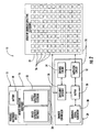
- the charger 14 illustratively includes a base 24 having an area larger than the device conductive footprint 22 and able to receive the portable electronic device 12 thereon in a plurality of different positions.
- the charger 14 may also include and an array of charger capacitive electrodes 26 and a base dielectric layer 25 carried by the base 24.
- the charger 14 further includes, for example, a charger controller 28 for selectively driving the charger capacitive electrodes 26 within the device conductive footprint 22 with a charging signal sufficient to capacitively charge the battery 18 of the portable electronic device 12, and not driving charger capacitive electrodes outside the device conductive footprint with the charging signal when the portable electronic device is positioned on the charger 14 to thereby capacitively charge the battery of the portable electronic device while reducing undesired (EMI).
- EMI undesired
- the charger controller 28 selectively drives the charger capacitive electrodes 26 within the device conductive footprint 22 with a charging signal while not driving the charger capacitive electrodes outside the device conductive footprint.
- the charger capacitive electrodes 26 being driven by the charging signal are covered by the device capacitive electrodes 20, the device capacitive electrodes function as an EMI shield as will be appreciated by those skilled in the art.
- a communication link 38 between the portable electronic device 12 and the computer 30 will be less likely to be disrupted by the operation of charger 14.
- the charger controller 28 may sense impedances, for example, of the charger capacitive electrodes 26 to determine whether a respective charger capacitive electrode is within the device conductive footprint 22 or not. Such sensing permits the charger controller 28 to accommodate the portable electronic device 12 if it is moved across the array of charger capacitive electrodes 26.
- the charger controller 28 may sequentially drive the charger capacitive electrodes 26 with a sensing signal to sense impedances thereof as will be appreciated by those skilled in the art.
- the charging signal may have an amplitude at least one hundred times greater than an amplitude of the sensing signal, for example.
- the control circuit 34 determines which charger capacitive electrodes 26 are within the device conductive footprint 22 by operating the charging signal generator 30 to generate a sensing signal.
- the impedance detector 36 senses a first impedance when a charger capacitive electrode 26 is within the device conductive footprint 22, and senses a second impedance when a charger capacitive electrode 26 is not. This sensing data is communicated to the control circuit 34
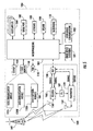
- FIG. 5 In addition to the processing device 1800, other parts of the mobile device 1000 are shown schematically in FIG. 5 . These include a communications subsystem 1001; a short-range communications subsystem 1020; the keyboard 1400 and the display 1600, along with other input/output devices 1060, 1080, 1100 and 1120; as well as memory devices 1160,1180 and various other device subsystems 1201.
- the mobile device 1000 is preferably a two-way RF communications device having voice and data communications capabilities.
- the mobile device 1000 preferably has the capability to communicate with other computer systems via the Internet.
Landscapes
- Engineering & Computer Science (AREA)
- Power Engineering (AREA)
- Computer Networks & Wireless Communication (AREA)
- Physics & Mathematics (AREA)
- Electromagnetism (AREA)
- Charge And Discharge Circuits For Batteries Or The Like (AREA)
Claims (13)
- Chargeur (14) pour charger par voie capacitive une batterie (18) dans un dispositif électronique portable (12) lorsque le dispositif électronique portable (12) est placé temporairement à proximité immédiate du chargeur (14), le chargeur (14) comportant :une base (24) ayant une étendue plus grande que le dispositif électronique portable (12) et capable de recevoir sur elle le dispositif électronique portable (12) dans plusieurs positions différentes ;un réseau d'électrodes capacitives (26) de charge portées par ladite base (24) ; etune unité de commande (28) de chargeur comprenant
un générateur (30) de signal de charge ;
un circuit de commutation (32) connecté entre ledit générateur (30) de signal de charge et lesdites électrodes capacitives (26) de chargeur ;
un circuit de commande (34) destiné à déterminer lesquelles desdites électrodes capacitives (26) de chargeur sont recouvertes par le dispositif électronique portable (12) en amenant le générateur (30) de signal de charge à générer un signal de détection ;
un tampon connecté entre ledit générateur (30) de signal de charge et ledit circuit de commutation (32) ; et
un détecteur d'impédance (36) destiné à capter l'impédance desdites électrodes capacitives (26) de chargeur ;
dans lequel ledit circuit de commande (34) est connecté audit circuit de commutation (12) ; et
ledit détecteur d'impédance (36) est connecté au tampon et au circuit de commande (34), et
ledit circuit de commande (34) est conçu pour utiliser ladite impédance captée par ledit détecteur d'impédance (36) pour attaquer sélectivement lesdites électrodes capacitives (26) de chargeur recouvertes par le dispositif électronique portable (12) avec un signal de charge suffisant pour charger par voie capacitive la batterie (18) du dispositif électronique portable (12) et sans attaquer les électrodes capacitives (26) de chargeur non recouvertes par le dispositif électronique portable (12) avec le signal de charge lorsque le dispositif électronique portable (12) est positionné sur ledit chargeur (14). - Chargeur selon la revendication 1, dans lequel ladite unité de commande (28) de chargeur attaque séquentiellement lesdites électrodes capacitives (26) de chargeur avec un signal de détection pour en capter les impédances.
- Chargeur selon la revendication 1, dans lequel le signal de charge a une amplitude au moins cent fois supérieure à l'amplitude du signal de détection.
- Appareil électronique (10) comportant le chargeur de la revendication 1, dans lequel :le dispositif électronique portable (12) peut être chargé par voie capacitive par le chargeur (14) lorsque ledit dispositif électronique portable (12) est placé temporairement à proximité immédiate dudit chargeur (14) ;ledit dispositif électronique portable comportant un boîtier (16), une batterie (18) portée par le boîtier, et au moins une paire d'électrodes capacitives (20) de dispositif portées par ledit boîtier pour charger ladite batterie (18) et définissant une empreinte conductrice (22) de dispositif et dans lequel :l'unité de commande (28) de chargeur est agencée pour attaquer sélectivement lesdites électrodes capacitives (26) de chargeur se trouvant dans l'empreinte conductrice de dispositif avec un signal de charge suffisant pour charger par voie capacitive la batterie et sans attaquer les électrodes capacitives (26) de chargeur en dehors de l'empreinte conductrice de dispositif avec le signal de charge lorsque ledit dispositif électronique portable (12) est positionné sur ledit chargeur (14) afin de charger par voie capacitive ladite batterie (18) dudit dispositif électronique portable (12) tout en réduisant les parasites électromagnétiques (EMI) indésirés.
- Appareil électronique selon la revendication 4, dans lequel ladite unité de commande (28) de chargeur capte les impédances desdites électrodes capacitives (26) de chargeur pour déterminer si une électrode capacitive respective (26) de chargeur se trouve à l'intérieur de l'empreinte conductrice de dispositif ou non.
- Appareil électronique selon la revendication 5, dans lequel ladite unité de commande (28) de chargeur attaque séquentiellement lesdites électrodes capacitives (26) de chargeur avec un signal de détection pour en capter les impédances.
- Appareil électronique selon la revendication 6, dans lequel le signal de charge a une amplitude au moins cent fois supérieure à l'amplitude du signal de détection.
- Appareil électronique selon la revendication 4, dans lequel ledit circuit de commande fait fonctionner ledit générateur (30) de signal de charge à une amplitude réduite pour qu'il serve de générateur de signal pour le signal de détection.
- Appareil électronique selon la revendication 4, dans lequel ladite unité de commande (28) de chargeur et ledit dispositif électronique portable (12) communiquent aussi par l'intermédiaire desdites électrodes capacitives (26) de chargeur.
- Procédé de charge par voie capacitive d'un dispositif électronique portable avec un chargeur, le dispositif électronique portable comportant un boîtier, une batterie portée par le boîtier, et au moins une paire d'électrodes capacitives de dispositif portées par le boîtier pour charger la batterie et définissant une empreinte conductrice de dispositif, et le chargeur comportant une base ayant une étendue plus grande que l'empreinte conductrice de dispositif et capable de recevoir sur elle le dispositif électronique portable dans plusieurs positions différentes, un réseau d'électrodes capacitives de chargeur portées par la base, et une unité de commande de chargeur connectée aux électrodes capacitives de chargeur, l'unité de commande de chargeur comprenant un générateur de signal de charge, un circuit de commutation connecté entre le générateur de signal de charge et les électrodes capacitives de chargeur, un circuit de commande connecté au circuit de commutation, un tampon connecté entre le générateur de signal de charge et le circuit de commutation, et un détecteur d'impédance connecté au tampon et au circuit de commande, le procédé comprenant :la mise en place temporaire du dispositif électronique portable à proximité immédiate du chargeur ; etl'attaque sélective, par l'intermédiaire de l'unité de commande de chargeur, des électrodes capacitives de chargeur se trouvant dans l'empreinte conductrice de dispositif avec un signal de charge suffisant pour charger par voie capacitive la batterie du dispositif électronique portable et sans attaquer des électrodes capacitives de chargeur situées en dehors de l'empreinte conductrice de dispositif avec le signal de charge pour charger ainsi par voie capacitive la batterie du dispositif électronique portable tout en réduisant les parasites électromagnétiques (EMI) indésirés.
- Procédé selon la revendication 10, comprenant en outre la détection, par l'intermédiaire de l'unité de commande de chargeur, des impédances des électrodes capacitives de chargeur afin de déterminer si une électrode capacitive respective de chargeur se trouve à l'intérieur de l'empreinte conductrice de dispositif ou non.
- Procédé selon la revendication 11, comprenant en outre l'attaque séquentielle, par l'intermédiaire de l'unité de commande de chargeur, des électrodes capacitives de chargeur avec un signal de détection pour en capter les impédances.
- Procédé selon la revendication 12, dans lequel le signal de charge a une amplitude au moins cent fois supérieure à l'amplitude du signal de détection.
Priority Applications (5)
| Application Number | Priority Date | Filing Date | Title |
|---|---|---|---|
| AT05250617T ATE427576T1 (de) | 2005-02-04 | 2005-02-04 | Vorrichtung und verfahren fur das aufladen einer batterie uber kapazitiver kopplung |
| EP05250617A EP1689062B1 (fr) | 2005-02-04 | 2005-02-04 | Dispositif et méthode pour charger une batterie par couplage capacitif |
| DE602005013635T DE602005013635D1 (de) | 2005-02-04 | 2005-02-04 | Vorrichtung und Verfahren für das Aufladen einer Batterie über kapazitiver Kopplung |
| US11/051,581 US7504802B2 (en) | 2005-02-04 | 2005-02-04 | Portable electronic device and capacitive charger therefor and associated methods |
| CA002526245A CA2526245C (fr) | 2005-02-04 | 2005-12-06 | Dispositif electronique portatif, chargeur capacitif pour ce dispositif et methodes connexes |
Applications Claiming Priority (1)
| Application Number | Priority Date | Filing Date | Title |
|---|---|---|---|
| EP05250617A EP1689062B1 (fr) | 2005-02-04 | 2005-02-04 | Dispositif et méthode pour charger une batterie par couplage capacitif |
Publications (2)
| Publication Number | Publication Date |
|---|---|
| EP1689062A1 EP1689062A1 (fr) | 2006-08-09 |
| EP1689062B1 true EP1689062B1 (fr) | 2009-04-01 |
Family
ID=34940429
Family Applications (1)
| Application Number | Title | Priority Date | Filing Date |
|---|---|---|---|
| EP05250617A Active EP1689062B1 (fr) | 2005-02-04 | 2005-02-04 | Dispositif et méthode pour charger une batterie par couplage capacitif |
Country Status (5)
| Country | Link |
|---|---|
| US (1) | US7504802B2 (fr) |
| EP (1) | EP1689062B1 (fr) |
| AT (1) | ATE427576T1 (fr) |
| CA (1) | CA2526245C (fr) |
| DE (1) | DE602005013635D1 (fr) |
Cited By (2)
| Publication number | Priority date | Publication date | Assignee | Title |
|---|---|---|---|---|
| DE102010015510A1 (de) * | 2010-04-20 | 2011-10-20 | Gira Giersiepen Gmbh & Co. Kg | System aus einer mobilen Einheit und einer Vorrichtung zum berührungslosen Laden der mobilen Einheit mit elektrischer Energie |
| JP2012095505A (ja) * | 2010-10-29 | 2012-05-17 | Murata Mfg Co Ltd | ワイヤレス電力伝送システムおよび送電装置 |
Families Citing this family (25)
| Publication number | Priority date | Publication date | Assignee | Title |
|---|---|---|---|---|
| US20090072782A1 (en) * | 2002-12-10 | 2009-03-19 | Mitch Randall | Versatile apparatus and method for electronic devices |
| JP4318044B2 (ja) | 2005-03-03 | 2009-08-19 | ソニー株式会社 | 電力供給システム、電力供給装置および方法、受電装置および方法、記録媒体、並びにプログラム |
| KR100792308B1 (ko) * | 2006-01-31 | 2008-01-07 | 엘에스전선 주식회사 | 코일 어레이를 구비한 무접점 충전장치, 무접점 충전시스템 및 충전 방법 |
| US7772802B2 (en) * | 2007-03-01 | 2010-08-10 | Eastman Kodak Company | Charging display system |
| FR2920061A1 (fr) * | 2007-08-17 | 2009-02-20 | Patrick Camurati | Procede et dispositif de transport, distribution et gestion de l'energie electrique par couplage longitudinal a distance en champ proche entre dipoles electriques |
| US20100201315A1 (en) * | 2007-09-27 | 2010-08-12 | Panasonic Corporation | Electronic device, charger, and charging device |
| JP4557049B2 (ja) * | 2008-06-09 | 2010-10-06 | ソニー株式会社 | 伝送システム、給電装置、受電装置、及び伝送方法 |
| US8626249B2 (en) * | 2008-08-12 | 2014-01-07 | T-Mobile Usa, Inc. | Charging station that operates as an intermediary device between mobile devices and other devices |
| KR101510760B1 (ko) * | 2009-01-19 | 2015-04-10 | 삼성전자 주식회사 | 디스플레이장치 및 그 제어 방법 |
| KR101782083B1 (ko) * | 2010-09-08 | 2017-09-27 | 삼성전자주식회사 | 공진 전력 전송을 이용한 지붕형 충전 장치 |
| JP5605153B2 (ja) * | 2010-10-15 | 2014-10-15 | ソニー株式会社 | 給電装置、給電方法および給電システム |
| JP5772501B2 (ja) * | 2011-10-25 | 2015-09-02 | 株式会社村田製作所 | 電力伝送システム |
| JP5839105B2 (ja) | 2012-02-22 | 2016-01-06 | 株式会社村田製作所 | 送電装置及び送電制御方法 |
| US10149711B2 (en) | 2012-03-30 | 2018-12-11 | Depuy Mitek, Llc | Surgical impact tool |
| KR101901720B1 (ko) * | 2012-04-02 | 2018-11-13 | 삼성전자주식회사 | 더미 장치와의 연동 방법 및 그 전자 장치 |
| US20140021798A1 (en) * | 2012-07-17 | 2014-01-23 | Witricity Corporation | Wireless energy transfer with repeater resonators |
| EP2903130B1 (fr) * | 2012-09-25 | 2017-05-31 | Fuji Machine Mfg. Co., Ltd. | Dispositif d'alimentation électrique sans contact couplé électrostatiquement et procédé de commande pour celui-ci |
| EP2903131B1 (fr) * | 2012-09-26 | 2022-03-02 | FUJI Corporation | Appareil d'alimentation électrique sans contact de type à couplage électrostatique |
| WO2014049868A1 (fr) * | 2012-09-28 | 2014-04-03 | 富士機械製造株式会社 | Appareil d'alimentation de système de couplage capacitif sans contact |
| US20140197782A1 (en) * | 2013-01-15 | 2014-07-17 | Lite-On It Corporation | Wireless charger with combined electric radiation shielding and capacitive sensing functions |
| JP6127777B2 (ja) | 2013-06-28 | 2017-05-17 | ソニー株式会社 | 給電装置および給電システム |
| CN105637727B (zh) * | 2013-08-15 | 2020-09-22 | 胡玛沃克斯公司 | 无线充电装置 |
| US10014705B2 (en) | 2015-04-02 | 2018-07-03 | Apple Inc. | Signal quality dependent throttling of devices for reducing electromagnetic interference |
| US10283952B2 (en) | 2017-06-22 | 2019-05-07 | Bretford Manufacturing, Inc. | Rapidly deployable floor power system |
| US11456623B2 (en) | 2020-11-04 | 2022-09-27 | Lagree Technologies, Inc. | Wireless power system for an exercise machine |
Family Cites Families (30)
| Publication number | Priority date | Publication date | Assignee | Title |
|---|---|---|---|---|
| US31118A (en) * | 1861-01-15 | Improvement in seeding-cultivators | ||
| GB8625429D0 (en) * | 1986-10-23 | 1986-11-26 | Philp R | Contactless electronic connectors |
| US4688097A (en) * | 1986-10-30 | 1987-08-18 | Jerrold Electronics Corp. | D.C.-coupled video clamping circuit |
| DE3906349A1 (de) | 1989-03-01 | 1990-09-13 | Hartmut Hennige | Verfahren und vorrichtung zur vereinfachung des gebrauchs einer vielzahl von kreditkarten u. dgl. |
| US5519262A (en) | 1992-11-17 | 1996-05-21 | Wood; Mark B. | Near field power coupling system |
| US5525843A (en) * | 1994-02-14 | 1996-06-11 | Ab Volvo | Seat occupant detection system |
| JP2671809B2 (ja) * | 1994-06-30 | 1997-11-05 | 日本電気株式会社 | 非接触型充電装置 |
| DE19519881C1 (de) | 1995-05-31 | 1996-07-18 | Grundig Emv | Anordnung zur Ladung von Akkus für ein schnurloses Telefon |
| US6067368A (en) | 1996-01-26 | 2000-05-23 | Authentec, Inc. | Fingerprint sensor having filtering and power conserving features and related methods |
| US5682032A (en) | 1996-02-22 | 1997-10-28 | Philipp; Harald | Capacitively coupled identity verification and escort memory apparatus |
| US5847447A (en) | 1996-07-09 | 1998-12-08 | Ambient Corporation | Capcitively coupled bi-directional data and power transmission system |
| JPH1092673A (ja) | 1996-07-26 | 1998-04-10 | Tdk Corp | 非接触電力伝送装置 |
| US6331744B1 (en) | 1998-02-10 | 2001-12-18 | Light Sciences Corporation | Contactless energy transfer apparatus |
| US6173899B1 (en) | 1998-04-03 | 2001-01-16 | Alexander Rozin | Method and system for contactless energy transmission and data exchange between a terminal and IC card |
| US6275681B1 (en) | 1998-04-16 | 2001-08-14 | Motorola, Inc. | Wireless electrostatic charging and communicating system |
| US6282407B1 (en) | 1998-04-16 | 2001-08-28 | Motorola, Inc. | Active electrostatic transceiver and communicating system |
| US6380711B2 (en) | 1999-06-30 | 2002-04-30 | Research In Motion Limited | Battery recharging device and method and an automatic battery detection system and method therefor |
| US6803744B1 (en) * | 1999-11-01 | 2004-10-12 | Anthony Sabo | Alignment independent and self aligning inductive power transfer system |
| DE20004691U1 (de) | 2000-03-14 | 2000-06-29 | Yang Wen Chin | Ladeeinrichtung mit USB-Schnittstelle für einen GSM-Telefon-Akkumulator |
| US6184651B1 (en) | 2000-03-20 | 2001-02-06 | Motorola, Inc. | Contactless battery charger with wireless control link |
| WO2001080444A1 (fr) * | 2000-04-18 | 2001-10-25 | Schleifring Und Apparatebau Gmbh | Dispositif de transfert d'energie electrique ou de signaux |
| DE10026173A1 (de) | 2000-04-18 | 2001-10-31 | Schleifring Und Appbau Gmbh | Power kontaktlos-Schaltregler |
| WO2001092900A1 (fr) * | 2000-05-26 | 2001-12-06 | Automotive Systems Laboratory, Inc. | Detecteur d'occupant |
| TW479393B (en) | 2000-09-27 | 2002-03-11 | Acer Peripherals Inc | Automatic USB charging apparatus and its operating method |
| US6362610B1 (en) | 2001-08-14 | 2002-03-26 | Fu-I Yang | Universal USB power supply unit |
| GB0213374D0 (en) * | 2002-06-10 | 2002-07-24 | Univ City Hong Kong | Planar inductive battery charger |
| US6614206B1 (en) | 2002-05-23 | 2003-09-02 | Palm, Inc. | Universal USB charging accessory |
| JP3905005B2 (ja) * | 2002-09-18 | 2007-04-18 | 富士通株式会社 | 携帯型機器及び半導体集積回路装置 |
| US6756765B2 (en) | 2002-10-08 | 2004-06-29 | Koninklijke Philips Electronics N.V. | System and method for charging users to recharge power supplies in portable devices |
| US7570994B2 (en) | 2003-04-25 | 2009-08-04 | Medtronic Physio-Control Corp. | Apparatus and method for maintaining a defibrillator battery charge and optionally communicating |
-
2005
- 2005-02-04 US US11/051,581 patent/US7504802B2/en active Active
- 2005-02-04 EP EP05250617A patent/EP1689062B1/fr active Active
- 2005-02-04 DE DE602005013635T patent/DE602005013635D1/de active Active
- 2005-02-04 AT AT05250617T patent/ATE427576T1/de not_active IP Right Cessation
- 2005-12-06 CA CA002526245A patent/CA2526245C/fr active Active
Cited By (3)
| Publication number | Priority date | Publication date | Assignee | Title |
|---|---|---|---|---|
| DE102010015510A1 (de) * | 2010-04-20 | 2011-10-20 | Gira Giersiepen Gmbh & Co. Kg | System aus einer mobilen Einheit und einer Vorrichtung zum berührungslosen Laden der mobilen Einheit mit elektrischer Energie |
| EP2381558A2 (fr) | 2010-04-20 | 2011-10-26 | GIRA GIERSIEPEN GmbH & Co. KG | Système constitué d'une unité mobile et d'un dispositif de chargement sans contact de l'unité mobile en énergie électrique |
| JP2012095505A (ja) * | 2010-10-29 | 2012-05-17 | Murata Mfg Co Ltd | ワイヤレス電力伝送システムおよび送電装置 |
Also Published As
| Publication number | Publication date |
|---|---|
| CA2526245A1 (fr) | 2006-02-20 |
| US20060176015A1 (en) | 2006-08-10 |
| CA2526245C (fr) | 2006-11-28 |
| ATE427576T1 (de) | 2009-04-15 |
| EP1689062A1 (fr) | 2006-08-09 |
| US7504802B2 (en) | 2009-03-17 |
| DE602005013635D1 (de) | 2009-05-14 |
Similar Documents
| Publication | Publication Date | Title |
|---|---|---|
| EP1689062B1 (fr) | Dispositif et méthode pour charger une batterie par couplage capacitif | |
| US7511452B2 (en) | Portable electronic device and capacitive charger providing data transfer and associated methods | |
| US7791311B2 (en) | Apparatus and method of wirelessly sharing power by inductive method | |
| CN104953626B (zh) | 局部计算环境中的无线电力使用 | |
| KR102012972B1 (ko) | 무선 전력 송수신 장치 | |
| US8368515B2 (en) | Dual mode RFID communication device operating as a reader or tag | |
| EP2495883B1 (fr) | Système nfc fournissant des fonctions de mesure du niveau d'alimentation de batterie et procédés associés | |
| EP1834394B1 (fr) | Procede et dispositif pour communications en champ proche | |
| US20100038970A1 (en) | Short Range Efficient Wireless Power Transfer | |
| JP2003070187A (ja) | 非接触データキャリア装置並びに内蔵二次電池の充電方法 | |
| CN101447684A (zh) | 无线电力充电系统 | |
| EP2568531B1 (fr) | Dispositif de communications mobile sans fil incluant un ajustement d'impédance basé sur le couplage acoustique et procédés correspondants | |
| KR101796788B1 (ko) | 에너지 전달 장치 및 방법 | |
| EP2579423B1 (fr) | Charge et communication sans fil avec des dispositifs d'alimentation et dispositifs d'alimentation dans un système de communication | |
| KR101973406B1 (ko) | 무선 전력 송수신 장치 및 무선 전력 송수신 방법 | |
| US20210226668A1 (en) | Antenna activation method for a near-field communication device | |
| KR20100019208A (ko) | 무선전파를 이용한 충전장치 | |
| CN111613762B (zh) | 电池组、电子设备和充放电控制方法 | |
| KR20150028397A (ko) | Nfc를 이용한 차량 내 무선전력 전송 방법 | |
| EP2546997A1 (fr) | Dispositif mobile de communications sans fil pour authentifier une source d'alimentation amovible via des communications NFC et procédés associés | |
| KR20170122906A (ko) | 무선 충전 시스템에서 무전원 상태의 수신기 초기 동작 방법 및 이를 위한 장치 | |
| KR20090072413A (ko) | 비접촉 전원 공급 시스템 | |
| JP2012205363A (ja) | 電子機器 |
Legal Events
| Date | Code | Title | Description |
|---|---|---|---|
| PUAI | Public reference made under article 153(3) epc to a published international application that has entered the european phase |
Free format text: ORIGINAL CODE: 0009012 |
|
| 17P | Request for examination filed |
Effective date: 20050215 |
|
| AK | Designated contracting states |
Kind code of ref document: A1 Designated state(s): AT BE BG CH CY CZ DE DK EE ES FI FR GB GR HU IE IS IT LI LT LU MC NL PL PT RO SE SI SK TR |
|
| AX | Request for extension of the european patent |
Extension state: AL BA HR LV MK YU |
|
| 17Q | First examination report despatched |
Effective date: 20070221 |
|
| AKX | Designation fees paid |
Designated state(s): AT BE BG CH CY CZ DE DK EE ES FI FR GB GR HU IE IS IT LI LT LU MC NL PL PT RO SE SI SK TR |
|
| AXX | Extension fees paid |
Extension state: YU Payment date: 20070122 Extension state: BA Payment date: 20070122 Extension state: AL Payment date: 20070122 Extension state: MK Payment date: 20070122 Extension state: HR Payment date: 20070122 Extension state: LV Payment date: 20070122 |
|
| GRAP | Despatch of communication of intention to grant a patent |
Free format text: ORIGINAL CODE: EPIDOSNIGR1 |
|
| GRAS | Grant fee paid |
Free format text: ORIGINAL CODE: EPIDOSNIGR3 |
|
| GRAA | (expected) grant |
Free format text: ORIGINAL CODE: 0009210 |
|
| AK | Designated contracting states |
Kind code of ref document: B1 Designated state(s): AT BE BG CH CY CZ DE DK EE ES FI FR GB GR HU IE IS IT LI LT LU MC NL PL PT RO SE SI SK TR |
|
| AX | Request for extension of the european patent |
Extension state: AL BA HR LV MK YU |
|
| REG | Reference to a national code |
Ref country code: GB Ref legal event code: FG4D |
|
| REG | Reference to a national code |
Ref country code: CH Ref legal event code: EP |
|
| REG | Reference to a national code |
Ref country code: IE Ref legal event code: FG4D |
|
| REF | Corresponds to: |
Ref document number: 602005013635 Country of ref document: DE Date of ref document: 20090514 Kind code of ref document: P |
|
| PG25 | Lapsed in a contracting state [announced via postgrant information from national office to epo] |
Ref country code: SI Free format text: LAPSE BECAUSE OF FAILURE TO SUBMIT A TRANSLATION OF THE DESCRIPTION OR TO PAY THE FEE WITHIN THE PRESCRIBED TIME-LIMIT Effective date: 20090401 |
|
| NLV1 | Nl: lapsed or annulled due to failure to fulfill the requirements of art. 29p and 29m of the patents act | ||
| PG25 | Lapsed in a contracting state [announced via postgrant information from national office to epo] |
Ref country code: FI Free format text: LAPSE BECAUSE OF FAILURE TO SUBMIT A TRANSLATION OF THE DESCRIPTION OR TO PAY THE FEE WITHIN THE PRESCRIBED TIME-LIMIT Effective date: 20090401 Ref country code: ES Free format text: LAPSE BECAUSE OF FAILURE TO SUBMIT A TRANSLATION OF THE DESCRIPTION OR TO PAY THE FEE WITHIN THE PRESCRIBED TIME-LIMIT Effective date: 20090712 Ref country code: EE Free format text: LAPSE BECAUSE OF FAILURE TO SUBMIT A TRANSLATION OF THE DESCRIPTION OR TO PAY THE FEE WITHIN THE PRESCRIBED TIME-LIMIT Effective date: 20090401 Ref country code: LT Free format text: LAPSE BECAUSE OF FAILURE TO SUBMIT A TRANSLATION OF THE DESCRIPTION OR TO PAY THE FEE WITHIN THE PRESCRIBED TIME-LIMIT Effective date: 20090401 Ref country code: AT Free format text: LAPSE BECAUSE OF FAILURE TO SUBMIT A TRANSLATION OF THE DESCRIPTION OR TO PAY THE FEE WITHIN THE PRESCRIBED TIME-LIMIT Effective date: 20090401 Ref country code: PT Free format text: LAPSE BECAUSE OF FAILURE TO SUBMIT A TRANSLATION OF THE DESCRIPTION OR TO PAY THE FEE WITHIN THE PRESCRIBED TIME-LIMIT Effective date: 20090902 |
|
| PG25 | Lapsed in a contracting state [announced via postgrant information from national office to epo] |
Ref country code: SE Free format text: LAPSE BECAUSE OF FAILURE TO SUBMIT A TRANSLATION OF THE DESCRIPTION OR TO PAY THE FEE WITHIN THE PRESCRIBED TIME-LIMIT Effective date: 20090701 Ref country code: NL Free format text: LAPSE BECAUSE OF FAILURE TO SUBMIT A TRANSLATION OF THE DESCRIPTION OR TO PAY THE FEE WITHIN THE PRESCRIBED TIME-LIMIT Effective date: 20090401 Ref country code: IS Free format text: LAPSE BECAUSE OF FAILURE TO SUBMIT A TRANSLATION OF THE DESCRIPTION OR TO PAY THE FEE WITHIN THE PRESCRIBED TIME-LIMIT Effective date: 20090801 Ref country code: PL Free format text: LAPSE BECAUSE OF FAILURE TO SUBMIT A TRANSLATION OF THE DESCRIPTION OR TO PAY THE FEE WITHIN THE PRESCRIBED TIME-LIMIT Effective date: 20090401 |
|
| PG25 | Lapsed in a contracting state [announced via postgrant information from national office to epo] |
Ref country code: CZ Free format text: LAPSE BECAUSE OF FAILURE TO SUBMIT A TRANSLATION OF THE DESCRIPTION OR TO PAY THE FEE WITHIN THE PRESCRIBED TIME-LIMIT Effective date: 20090401 Ref country code: DK Free format text: LAPSE BECAUSE OF FAILURE TO SUBMIT A TRANSLATION OF THE DESCRIPTION OR TO PAY THE FEE WITHIN THE PRESCRIBED TIME-LIMIT Effective date: 20090401 Ref country code: RO Free format text: LAPSE BECAUSE OF FAILURE TO SUBMIT A TRANSLATION OF THE DESCRIPTION OR TO PAY THE FEE WITHIN THE PRESCRIBED TIME-LIMIT Effective date: 20090401 |
|
| PLBE | No opposition filed within time limit |
Free format text: ORIGINAL CODE: 0009261 |
|
| STAA | Information on the status of an ep patent application or granted ep patent |
Free format text: STATUS: NO OPPOSITION FILED WITHIN TIME LIMIT |
|
| PG25 | Lapsed in a contracting state [announced via postgrant information from national office to epo] |
Ref country code: BE Free format text: LAPSE BECAUSE OF FAILURE TO SUBMIT A TRANSLATION OF THE DESCRIPTION OR TO PAY THE FEE WITHIN THE PRESCRIBED TIME-LIMIT Effective date: 20090401 Ref country code: SK Free format text: LAPSE BECAUSE OF FAILURE TO SUBMIT A TRANSLATION OF THE DESCRIPTION OR TO PAY THE FEE WITHIN THE PRESCRIBED TIME-LIMIT Effective date: 20090401 |
|
| 26N | No opposition filed |
Effective date: 20100105 |
|
| PG25 | Lapsed in a contracting state [announced via postgrant information from national office to epo] |
Ref country code: BG Free format text: LAPSE BECAUSE OF FAILURE TO SUBMIT A TRANSLATION OF THE DESCRIPTION OR TO PAY THE FEE WITHIN THE PRESCRIBED TIME-LIMIT Effective date: 20090701 |
|
| REG | Reference to a national code |
Ref country code: CH Ref legal event code: PL |
|
| PG25 | Lapsed in a contracting state [announced via postgrant information from national office to epo] |
Ref country code: GR Free format text: LAPSE BECAUSE OF FAILURE TO SUBMIT A TRANSLATION OF THE DESCRIPTION OR TO PAY THE FEE WITHIN THE PRESCRIBED TIME-LIMIT Effective date: 20090702 Ref country code: CH Free format text: LAPSE BECAUSE OF NON-PAYMENT OF DUE FEES Effective date: 20100228 Ref country code: LI Free format text: LAPSE BECAUSE OF NON-PAYMENT OF DUE FEES Effective date: 20100228 Ref country code: MC Free format text: LAPSE BECAUSE OF NON-PAYMENT OF DUE FEES Effective date: 20100301 |
|
| PG25 | Lapsed in a contracting state [announced via postgrant information from national office to epo] |
Ref country code: IE Free format text: LAPSE BECAUSE OF NON-PAYMENT OF DUE FEES Effective date: 20100204 |
|
| PG25 | Lapsed in a contracting state [announced via postgrant information from national office to epo] |
Ref country code: IT Free format text: LAPSE BECAUSE OF FAILURE TO SUBMIT A TRANSLATION OF THE DESCRIPTION OR TO PAY THE FEE WITHIN THE PRESCRIBED TIME-LIMIT Effective date: 20090401 |
|
| PG25 | Lapsed in a contracting state [announced via postgrant information from national office to epo] |
Ref country code: CY Free format text: LAPSE BECAUSE OF FAILURE TO SUBMIT A TRANSLATION OF THE DESCRIPTION OR TO PAY THE FEE WITHIN THE PRESCRIBED TIME-LIMIT Effective date: 20090401 |
|
| PG25 | Lapsed in a contracting state [announced via postgrant information from national office to epo] |
Ref country code: LU Free format text: LAPSE BECAUSE OF NON-PAYMENT OF DUE FEES Effective date: 20100204 Ref country code: HU Free format text: LAPSE BECAUSE OF FAILURE TO SUBMIT A TRANSLATION OF THE DESCRIPTION OR TO PAY THE FEE WITHIN THE PRESCRIBED TIME-LIMIT Effective date: 20091002 |
|
| PG25 | Lapsed in a contracting state [announced via postgrant information from national office to epo] |
Ref country code: TR Free format text: LAPSE BECAUSE OF FAILURE TO SUBMIT A TRANSLATION OF THE DESCRIPTION OR TO PAY THE FEE WITHIN THE PRESCRIBED TIME-LIMIT Effective date: 20090401 |
|
| REG | Reference to a national code |
Ref country code: DE Ref legal event code: R082 Ref document number: 602005013635 Country of ref document: DE Representative=s name: MERH-IP MATIAS ERNY REICHL HOFFMANN, DE |
|
| REG | Reference to a national code |
Ref country code: DE Ref legal event code: R082 Ref document number: 602005013635 Country of ref document: DE Representative=s name: MERH-IP MATIAS ERNY REICHL HOFFMANN, DE Effective date: 20140925 Ref country code: DE Ref legal event code: R081 Ref document number: 602005013635 Country of ref document: DE Owner name: BLACKBERRY LIMITED, WATERLOO, CA Free format text: FORMER OWNER: RESEARCH IN MOTION LTD., WATERLOO, ONTARIO, CA Effective date: 20140925 Ref country code: DE Ref legal event code: R082 Ref document number: 602005013635 Country of ref document: DE Representative=s name: MERH-IP MATIAS ERNY REICHL HOFFMANN PATENTANWA, DE Effective date: 20140925 |
|
| REG | Reference to a national code |
Ref country code: FR Ref legal event code: PLFP Year of fee payment: 12 |
|
| REG | Reference to a national code |
Ref country code: FR Ref legal event code: PLFP Year of fee payment: 13 |
|
| REG | Reference to a national code |
Ref country code: FR Ref legal event code: PLFP Year of fee payment: 14 |
|
| PGFP | Annual fee paid to national office [announced via postgrant information from national office to epo] |
Ref country code: FR Payment date: 20230223 Year of fee payment: 19 |
|
| PGFP | Annual fee paid to national office [announced via postgrant information from national office to epo] |
Ref country code: DE Payment date: 20240228 Year of fee payment: 20 Ref country code: GB Payment date: 20240220 Year of fee payment: 20 |