EP1688960B1 - Automatic calibration of electron multiplying CCDs - Google Patents
Automatic calibration of electron multiplying CCDs Download PDFInfo
- Publication number
- EP1688960B1 EP1688960B1 EP06075126A EP06075126A EP1688960B1 EP 1688960 B1 EP1688960 B1 EP 1688960B1 EP 06075126 A EP06075126 A EP 06075126A EP 06075126 A EP06075126 A EP 06075126A EP 1688960 B1 EP1688960 B1 EP 1688960B1
- Authority
- EP
- European Patent Office
- Prior art keywords
- gain
- electron multiplier
- signal
- charge
- test signal
- Prior art date
- Legal status (The legal status is an assumption and is not a legal conclusion. Google has not performed a legal analysis and makes no representation as to the accuracy of the status listed.)
- Active
Links
- 238000001444 catalytic combustion detection Methods 0.000 title 1
- 238000000034 method Methods 0.000 claims abstract description 46
- 238000012360 testing method Methods 0.000 claims abstract description 32
- 238000012546 transfer Methods 0.000 claims description 47
- 230000004044 response Effects 0.000 claims description 9
- 238000004590 computer program Methods 0.000 claims description 5
- 230000000737 periodic effect Effects 0.000 claims 2
- 238000005259 measurement Methods 0.000 description 28
- 238000003860 storage Methods 0.000 description 14
- 230000000694 effects Effects 0.000 description 8
- 230000003679 aging effect Effects 0.000 description 5
- 238000013461 design Methods 0.000 description 5
- 230000001419 dependent effect Effects 0.000 description 4
- 230000005684 electric field Effects 0.000 description 4
- 238000004458 analytical method Methods 0.000 description 3
- 238000004519 manufacturing process Methods 0.000 description 3
- 239000000463 material Substances 0.000 description 3
- 239000004065 semiconductor Substances 0.000 description 3
- VYPSYNLAJGMNEJ-UHFFFAOYSA-N Silicium dioxide Chemical compound O=[Si]=O VYPSYNLAJGMNEJ-UHFFFAOYSA-N 0.000 description 2
- XUIMIQQOPSSXEZ-UHFFFAOYSA-N Silicon Chemical compound [Si] XUIMIQQOPSSXEZ-UHFFFAOYSA-N 0.000 description 2
- 230000032683 aging Effects 0.000 description 2
- XAGFODPZIPBFFR-UHFFFAOYSA-N aluminium Chemical compound [Al] XAGFODPZIPBFFR-UHFFFAOYSA-N 0.000 description 2
- 229910052782 aluminium Inorganic materials 0.000 description 2
- 239000004411 aluminium Substances 0.000 description 2
- 238000001816 cooling Methods 0.000 description 2
- 230000001186 cumulative effect Effects 0.000 description 2
- 230000007423 decrease Effects 0.000 description 2
- 230000003287 optical effect Effects 0.000 description 2
- 230000005855 radiation Effects 0.000 description 2
- 229910052710 silicon Inorganic materials 0.000 description 2
- 239000010703 silicon Substances 0.000 description 2
- 101000694017 Homo sapiens Sodium channel protein type 5 subunit alpha Proteins 0.000 description 1
- 102100027198 Sodium channel protein type 5 subunit alpha Human genes 0.000 description 1
- 230000003466 anti-cipated effect Effects 0.000 description 1
- 238000003491 array Methods 0.000 description 1
- 230000008901 benefit Effects 0.000 description 1
- 230000008859 change Effects 0.000 description 1
- 238000007796 conventional method Methods 0.000 description 1
- 230000001955 cumulated effect Effects 0.000 description 1
- 230000003247 decreasing effect Effects 0.000 description 1
- 238000001514 detection method Methods 0.000 description 1
- 238000009826 distribution Methods 0.000 description 1
- 239000003574 free electron Substances 0.000 description 1
- 230000000977 initiatory effect Effects 0.000 description 1
- 238000002347 injection Methods 0.000 description 1
- 239000007924 injection Substances 0.000 description 1
- 230000002452 interceptive effect Effects 0.000 description 1
- 230000007246 mechanism Effects 0.000 description 1
- 230000008569 process Effects 0.000 description 1
- 230000001737 promoting effect Effects 0.000 description 1
- 108090000623 proteins and genes Proteins 0.000 description 1
- 230000009467 reduction Effects 0.000 description 1
- 238000012552 review Methods 0.000 description 1
- 238000013214 routine measurement Methods 0.000 description 1
- 230000035945 sensitivity Effects 0.000 description 1
- 235000012239 silicon dioxide Nutrition 0.000 description 1
- 239000000377 silicon dioxide Substances 0.000 description 1
- 238000003530 single readout Methods 0.000 description 1
- 239000007787 solid Substances 0.000 description 1
- 239000000243 solution Substances 0.000 description 1
- 239000000758 substrate Substances 0.000 description 1
Images

Classifications
-
- H—ELECTRICITY
- H04—ELECTRIC COMMUNICATION TECHNIQUE
- H04N—PICTORIAL COMMUNICATION, e.g. TELEVISION
- H04N17/00—Diagnosis, testing or measuring for television systems or their details
- H04N17/002—Diagnosis, testing or measuring for television systems or their details for television cameras
-
- G—PHYSICS
- G11—INFORMATION STORAGE
- G11C—STATIC STORES
- G11C19/00—Digital stores in which the information is moved stepwise, e.g. shift registers
- G11C19/28—Digital stores in which the information is moved stepwise, e.g. shift registers using semiconductor elements
- G11C19/282—Digital stores in which the information is moved stepwise, e.g. shift registers using semiconductor elements with charge storage in a depletion layer, i.e. charge coupled devices [CCD]
- G11C19/285—Peripheral circuits, e.g. for writing into the first stage; for reading-out of the last stage
-
- H—ELECTRICITY
- H04—ELECTRIC COMMUNICATION TECHNIQUE
- H04N—PICTORIAL COMMUNICATION, e.g. TELEVISION
- H04N25/00—Circuitry of solid-state image sensors [SSIS]; Control thereof
-
- H—ELECTRICITY
- H04—ELECTRIC COMMUNICATION TECHNIQUE
- H04N—PICTORIAL COMMUNICATION, e.g. TELEVISION
- H04N25/00—Circuitry of solid-state image sensors [SSIS]; Control thereof
- H04N25/70—SSIS architectures; Circuits associated therewith
- H04N25/71—Charge-coupled device [CCD] sensors; Charge-transfer registers specially adapted for CCD sensors
- H04N25/713—Transfer or readout registers; Split readout registers or multiple readout registers
-
- H—ELECTRICITY
- H04—ELECTRIC COMMUNICATION TECHNIQUE
- H04N—PICTORIAL COMMUNICATION, e.g. TELEVISION
- H04N25/00—Circuitry of solid-state image sensors [SSIS]; Control thereof
- H04N25/70—SSIS architectures; Circuits associated therewith
- H04N25/71—Charge-coupled device [CCD] sensors; Charge-transfer registers specially adapted for CCD sensors
- H04N25/72—Charge-coupled device [CCD] sensors; Charge-transfer registers specially adapted for CCD sensors using frame transfer [FT]
-
- H—ELECTRICITY
- H10—SEMICONDUCTOR DEVICES; ELECTRIC SOLID-STATE DEVICES NOT OTHERWISE PROVIDED FOR
- H10F—INORGANIC SEMICONDUCTOR DEVICES SENSITIVE TO INFRARED RADIATION, LIGHT, ELECTROMAGNETIC RADIATION OF SHORTER WAVELENGTH OR CORPUSCULAR RADIATION
- H10F39/00—Integrated devices, or assemblies of multiple devices, comprising at least one element covered by group H10F30/00, e.g. radiation detectors comprising photodiode arrays
- H10F39/10—Integrated devices
- H10F39/12—Image sensors
- H10F39/15—Charge-coupled device [CCD] image sensors
- H10F39/153—Two-dimensional or three-dimensional array CCD image sensors
Definitions
- the invention relates to electron multiplying structures, especially but not exclusively when used in Charge Coupled Devices (CCDs), and in particular to the calibration of same.
- CCDs Charge Coupled Devices
- EMCCD Electron Multiplying Charge Coupled Device
- EMCCD Electron Multiplying Charge Coupled Device
- Examples of known EMCCDs are provided by E2V under the Trade Mark L3Vision, and by Texas Instruments under the Trade Mark Impactron.
- EMCCDs may be used in cameras, or other apparatus, to capture images, or other optical data, by means of the photoelectric effect.
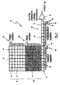
- FIG. 1 shows a schematic view of a conventional Frame Transfer EMCCD, generally indicated as 10.
- the EMCCD 10 comprises an array 12 of photoelectric cells 14, or photodetectors. These are commonly referred to as pixels.
- the array 12 typically comprises a conventional CCD array.
- the array 12 is commonly a two dimensional array, the number of rows and columns varying from device to device. In some cases, the array may be one dimensional, i.e. may comprise a single row of cells 14. In some CCD types, the array 12 may include a first, or image, section 16 and a second, or storage, section 18.
- each cell 14 During use, photons impinge upon the cells 14 in the image area 16, each cell 14 generating one or more electrons, i.e. a quantity of electrical charge, (by means of photo-generated electron-hole pairs the photoelectric effect) depending on the level of incident radiation.
- Each cell 14, and more particularly the data derived therefrom provides an element, or pixel, of each image, or other data set, captured by the EMCCD 10.
- the second section 18 of the array may be referred to as the storage area, the data, or charge, generated at the image area 16 being transferred or shifted to the storage area 18 after capture.
- the cells 14 of the storage area 18 are usually masked, typically with a deposited layer of aluminium, to prevent photons from impinging thereon.
- a shift register 20 normally a serial shift register, comprising a plurality of cells or stages 23 is associated with the array 12, through which data is read from the array 12 during use.
- data in the form of electrons or charge, is transferred from the array 12 into the shift register 20 one row at a time.
- one end 22 of the shift register 20 is connected to a charge to voltage amplifier 24, the data in the register 20 being shifted serially out of the shift register 20, via end 22, and through the amplifier 24 producing output signal 29.
- the cells 14 and register 20 are formed from any suitable semiconductor material and the shifting, or transfer, of electrons, or charge, from one cell 14, 23 to another is effected by control signals in the preferred form of clock signals.
- the clock signals normally take the form of voltage signals which, by appropriate manipulation of the electric fields in the cells 14, 23, cause the electrons to move, or transfer between cells 14, 23.
- the transfer of data, or electrons, from image area 16 of the array 12 to the storage area 18 is controlled by a combined clocking of a first set of clock signals (applied at inputs 50) and a second set of clock signals (applied at inputs 52).
- each set of clock signals comprises at least two (sometimes three or four) clock signals, each signal within a set usually being referred to as a phase, each respective set being applied, in use, to each respective cell or stage 14, 23.
- the key distinguishing feature of an EMCCD in comparison with a conventional CCD is the provision of a structure 26 between the end 22 of the shift register 20 and the output amplifier 24.
- the structure normally comprises a solid state electron multiplier and is commonly referred to as the EM gain register or Charge Multiplication Register.
- the EM gain register 26 normally takes the form of a shift register, usually a serial shift register, that may be generally similar to shift register 20 and so comprises a plurality of stages or cells 27.
- the transfer of data, or electrons, through or from the EM gain register 26 is controlled by a fourth set of clock signals (applied at inputs 56).
- FIGS. 2A and 2B show a schematic representation of a portion of a shift register, generally indicated as 21, that is suitable for use as the EM gain register 26.
- a plurality of electrodes or terminals 28 are associated with the register 21 for applying control signals to the register 21.
- Adjacent terminals 28 supply different or respective control signals so that a potential difference is created between adjacent terminals 28.
- the potential difference between adjacent terminals 28 creates an electric field at the associated portion of the register 21 thereby causing electrons to move, or transfer, along the register 21 from one stage or cell to the next. This is known as charge transfer.
- charge transfer By appropriate co-ordination of the control signals, electrons can be shifted along the register 21 to the output of the register 21 to create an output signal for supplying to the amplifier 24. Hence, the data obtained from the array 12 is shifted along the register 21.
- control signals include three voltage clock signals, or phases, that may be designated as R1, R2 and R3 (alternatively there may be 2 or more phases and corresponding control signals).
- each phase is applied, via a respective terminal 28, to each stage or cell of the register 21 in a fixed sequence (e,g, R1, R2, R3).
- the shift register 21 may serve as an EM gain register, an additional terminal 28A is provided for each stage or cell, the additional terminal 28A supplying a fixed reference signal (e.g. a d,c, signal).
- a fixed reference signal e.g. a d,c, signal.
- electrode 28A is provided between the electrodes that supply the R1 and R2 phases.
- Electrode 28A is held, during use, at a fixed potential and the adjacent electrode 28B (which in this example applies the R2 phase) is clocked, i.e, supplies a clock signal for the R2 phase, as normal, except that a higher voltage amplitude is used than is necessary for charge transfer alone.
- the clock amplitudes are typically 6 to 15V depending on actual CCD and its exact design, and those required for EM gain are typically 20V to 50V depending on actual CCD and its exact design.
- the multiplication of electrons per transfer is relatively small, typically around X1.01 to X1.015.
- the EM gain is a function of the EM voltage and of the operating temperature, the gain can typically be measured by taking the ratio of a given signal, e.g. a test signal, with the gain on and then with the gain off. Gain off can be achieved by using a lower clock amplitude at electrode 28B, i.e. an amplitude substantially the same or similar to that used for normal charge transfer in a CCD.
- the test signal is typically derived from a test image generated from a stable light source - no radiometric source or specific wavelength is required since only a ratio of the charge generated needs to be determined. Calibration of the EMCCD 10 at the time of manufacture, i.e.
- factory calibration typically involves measuring the EM gain for different EM clock voltages and temperatures and then using this information to adjust the operating EM voltage range to give the desired performance.
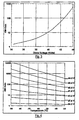
- the dependence of EM gain on clock amplitude (or more specifically on the EM voltage) is very sharp (see Figure 3 , noting the log scale which shows typical EM gain as a function of EM clock voltage for a specific EMCCD) and so requires stable electronic design.
- the dependence on temperature is less sharp but good operating temperature stability is also required (see Figure 4 which shows typical EM gain as a function of temperature for different EM clock voltages).
- Some EMCCDs do have a particular problem, commonly known as the ageing effect, whereby the EM gain decreases with usage.
- usage relates to the cumulative amount of charge accelerated through the EM field.
- the ageing effect appears to be dependent on the amount of charge passed through the EM gain register 26 combined with the EM field strength that the charge is transferred through. It also appears to be very strongly dependent on the EM field strength and so, when the EMCCD 10 is operated at high EM gains, the ageing rate can be disproportionately greater. Fortunately it has been observed that the ageing effect itself decreases with time meaning that with proper use the device should remain useful for many years.
- the temperature dependence of the EM gain is not a significant problem because it does not change with time and is not sharply dependent on temperature. Therefore any re-calibration of the EM clock amplitude, or EM voltage, can be done at one temperature and extrapolated to other temperatures.
- the only proviso is that the temperature chosen should ideally be within the range of anticipated operating temperatures. High-end cameras would typically be operated at between -50°C and -100°C, whereas volume market cameras would be operated typically between -20°C and 0°C.
- any calibration procedure needs to be carefully controlled. This may be relatively straightforward at the time of manufacture, but is problematic when performed at the user's site, especially when being performed by an inexperienced user. Regular factory recalibrations are a solution, but this would necessitate the apparatus containing the EMCCD, typically a camera, being returned to the factory, and, in any event, the user cannot know that calibration is required without measuring the EM gain.
- JP 2003009000 discloses a method of determining the gain of an electron multiplier as set out in the pre-characterising portion of Claim 1.
- a problem with JP2003009000 is that its gain determining method is unsuitable for use in cases where the CCD is held at relatively low temperatures.
- a first aspect of the invention provides a method of determining the gain of an electron multiplier, the electron multiplier as claimed in Claim 1.
- the test signal comprises, or is derived from, dark charge or dark current.
- the test signal comprises, or is derived from, clock induced charge (CIC), or spurious charge.
- Dark charge is the charge or electrons that accumulate as a result of darkcurrent.
- CIC is also known as Spurious Charge.
- the method includes causing the test signal to be input to the electron multiplier when the gain of the electron multiplier is enabled and when the gain of the electron multiplier is disabled, and said gain being determined by comparing the output of the electron multiplier in response to said test signal when the gain of the electron multiplier is enabled to the output of the electron multiplier in response to said test signal when the gain of the electron multiplier is disabled.
- the method may further include increasing or promoting darkcurrent and/or CIC in said device.
- This may be achieved by any suitable means, for example by appropriate selection and/or configuration of one or more control, or clock, signals that effect the transfer of charge in said device.
- control, or clock signals that effect the transfer of charge in said device.
- said clock signals For example, by setting one or more of said clock signals to have an amplitude that is sufficiently high to promote CIC during charge transfer. Typically, the amplitude is at least 25% and preferably at least 50% above the amplitude normally used to effect charge transfer.
- Darkcurrent may, for example, be increased by arranging for one or more of said clock signals to be unpinned (this can result in darkcurrent increases of 1 to 2 orders of magnitude).
- CIC may alternatively or additionally be promoted by increasing the periods of at least one of said clock signals, typically to the order of more than 10 and preferably several tens of milliseconds.
- the gain of the electron multiplier is determined by analysing the characteristics of the output of the electron multiplier in response to said test signal when the gain of the electron multiplier is enabled.
- said characteristics include events caused by the input of respective single electrons to said electron multiplier.
- the analysis may involve comparing the characteristics of the detected or measured output against known output results (e.g. by curve fitting or other mathematical techniques) or predicted output results (e.g. by curve fitting or other mathematical techniques).
- the method further includes adjusting the gain of the electron multiplier in response to the determined, or measured, gain.
- a second aspect of the invention provides an apparatus for detecting the gain of an electron multiplier, the apparatus comprising means for causing a test signal to be input to the electron multiplier from a device comprising at least one photodetector; and means for determining the gain of the electron multiplier from the output of the electron multiplier, wherein said test signal comprises, or is derived from, electrical charge generated by said at least one photodetector other than as a result of the incidence of an electromagnetic signal on said at least one photodetector.
- the apparatus includes at least one CCD or EMCCD.
- a third aspect of the invention provides an apparatus comprising at least one charge coupled device (CCD) and an electron multiplier, the electron multiplier being arranged to multiply, in use, signals received from the at least one CCD, the apparatus further including an apparatus of the second aspect of the invention.
- CCD charge coupled device
- the method of the invention may be implemented wholly or partially by computer software, or computer program code, which may be executed by a microprocessor, microcontroller or other computer included in or associated with the apparatus.
- a fourth aspect of the invention provides a computer program product comprising computer program code for causing a computer to perform the method of the first aspect of the invention.
- the invention may be employed with an EMCCD of the general type shown in Figure 1 , or with any other CCD type, e.g. frame transfer (FT), interline, full-frame (FF), Frame Interline (FI) and others.
- FT frame transfer
- FF full-frame
- FI Frame Interline
- Means for determining when the EM gain has fallen off, or decreased, is provided.
- means for re-calibrating, or adjusting, the EM gain is also provided.
- the selected method of calibration may depend on the exact usage of the camera (or other apparatus of which the EMCCD forms part). For example, there are two typical uses of an EMCCD-based apparatus (e.g. a camera):
- any calibration involves having means for measuring the EM gain.
- EM gain measurement it needs to be possible to feed a quantity of controlled charge, i.e. one or more electrons, into the gain register 26. Where this charge comes from does not matter and the most obvious source is an external optical signal. Conventionally, this would comprise an external, stabilised light source that could be attached to the camera without any light leaks.
- Some CCDs are provided with charge injection gate (CIG) structures built into the device itself. CIGs could be used to provide the charge, although current EMCCDs tend not to contain CIGs and, in any event, existing CIGs are not ideal for this purpose. New designs could include such or similar structures specifically designed for EM gain calibration purposes.
- CIG charge injection gate
- a stabilised light source could be built into the apparatus/camera, and this has been done before (for non-EMCCD cameras) for other reasons. This would work, but has some problems, the main problems being that the internal light source must not interfere with the incoming light when in normal use, and the additional cost.
- CIC darkcurrent and/or Clock Induced Charge
- Clock Induced Charge also known as Spurious Charge
- Spurious Charge is the occasional generation of charge during the normal clocking process. This phenomenon is not unique to EMCCDs and exists in all types of CCDs but, when a CCD or EMCCD is properly operated, the amounts of charge generated can be negligibly small, e.g. only one electron may be generated for every 10 or 100 transfers, or even less.
- Darkcurrent sometimes referred to as leakage current, comprises background signals or current that are present in a CCD or EMCCD and which do not result from the incidence of radiation on the CCD/EMCCD array. Darkcurrent arises primarily as a result of thermally produced free electrons.
- Method 1 may be used in cases where there is sufficient darkcurrent and/or CIC. Conventionally, it may be thought that this would limit the method to modestly cooled apparatus/cameras, say -30°C and above. This is not so, as is explained below. Normally, EMCCD equipment manufacturers strive to minimise both darkcurrent and CIC by deep cooling (usually below-50°C) and by careful clocking of the CCD chip respectively. In high-end apparatus/cameras, the usual levels of darkcurrent and CIC are very low and in practice it would take hours, or perhaps days, to capture enough charge to perform calibration with useful accuracy.
- a CCD/EMCCD can be operated so as to increase either darkcurrent or CIC or both above the levels that are typically present during normal use.
- darkcurrent can be increased by using an unpinned (non-inverted mode) clocking pattern or signal.
- Higher clock amplitudes than would normally be used when clocking a CCD may be used to increase CIC.
- the normal amplitude of the clock signal is in the region of 10 to 12V, then an increase of amplitude to approximately 15V or more should effect the desired increase in CIC.
- changing clock periods can increase CIC.
- the clock period may be increased (in comparison with the period of the clock signal used during normal operation of the CCD) to a length that promotes CIC. This is typically tens of microseconds as compared to a few microseconds or less as used for normal charge transfers.
- the former option can generate very large amounts of signal, up to 1 electron per transfer without exceeding the maximum electrode voltage rating.
- CIC generation is largely independent of CCD temperature, which is important for deep cooled systems where darkcurrent may be too small to be of practical use. It is a common misconception that CIC is very temperature dependant because it is well known that Impact Ionization is very dependant on temperature, but when the negative temperature dependence of state lifetimes is taken into account, CIC generation is found to be only slightly dependant on temperature.
- Methods of increasing CIC may be applied to any part or combination of two or more parts of the EMCCD 10 including the image area 16, storage area 18, the serial register(s) 20 and/or EM gain register(s) 26.
- Various normal CCD readout methods, or combinations thereof, of integrating, binning and/or accumulating may also be used to facilitate the measurement. This means that an accurate calibration of the EM gain can be performed in a short time without the need of any external stabilised light source or other external apparatus. In some cases, the user/operator may have to ensure that the camera is in darkness when the EM gain measurement/calibration is being performed.
- the entire operation can be performed without any user input apart from initiating the measurement/calibration routine (which would typically involve causing the shutter to close.)
- FT frame transfer CCDs
- interline CCDs even a shutter may not be required since each CCD type has a storage area that is covered (usually by a directly applied mask, typically formed from aluminium) and these areas can be used to generate the increased CIC or darkcurrent.
- the image area 16 would not be clocked and, when present, antiblooming features of the CCD 10 would drain any excess charge being generated in the image area.
- controlling computer typically a PC or other external computer but may alternatively or additionally comprise an on-board microprocessor, that controls, amongst other things, the operation of the EMCCD 10 including the clock signals, may be programmed to use its real-time clock to automatically and periodically alert the user to run the calibration/gain measurement procedure.
- the controlling computer may be programmed to use its real-time clock to automatically check and then automatically adjust the EM gain at predetermined intervals without the user ever needing to be aware. This automatic check and calibration may be performed at times that would not interfere with the normal intended usage of the apparatus/camera, for example, after execution of the camera software or during the night for continually operating systems.
- the EMCCD 10 comprises a known off the-shelf EMCCD chip, namely the CCD97 as supplied by E2V.
- the calibration of EM voltage versus EM gain is performed for a single CCD operating temperature. The same calibration can be performed for other temperatures, but as indicated above this may not be necessary.
- the CCD97 is an FT CCD device comprising an active image area of 512 by 512 pixels, and is similar to the EMCCD illustrated in Figure 1 . It has a maximum pixel readout speed of 11MHz with a readout noise of 60 electrons RMS but does not have antiblooming. A full datasheet can be obtained from the e2v.com website. In this example, it is also assumed that the most demanding case of low temperature operation is between -50°C and 100°C since at these temperatures, the darkcurrent will be too low to be of practical use. At such temperatures, it is proposed to use a CIC generated signal.
- each cell 14 produces, in the form of CIC, 0.5 electrons (a typical value for this CCD and a value that is adopted for illustration purposes hereafter) per vertical transfer (i.e. a transfer downwardly (as viewed in Figure 1 ) towards the register 20).
- This clock amplitude is approximately 4 volts above that required for normal charge transfer operation and low CIC.
- the array 12 must be substantially isolated from incident light. This may be achieved by closing the shutter or, if the apparatus/camera has no shutter, by placing the apparatus/camera in darkness. Since the CCD97 does not have antiblooming, the shielded storage area 18 alone will not be used to make the EM gain measurement because any light falling on the image area could cause charge, thus generated, to bloom out of the image area into the storage area during the EM gain measurement. Therefore, the array 12 must be kept in darkness.
- a series of 'keep clean' scans are performed to remove any residual photo-generated charge that may be present in the EMCCD 10.
- the scans may comprise any of a wide range of readout operations so long as they readout the whole EMCCD 10.
- the output signal 29 is measured or recorded without EM gain being effected. This may be achieved by setting the control or clock signals 56 for the EM gain register 26 such that charge transfer is effected but that the EM voltage does not cause Impact Ionization. In the illustrated example, this may achieved by using a clock signal at the electrodes 28B with an amplitude used normally to effect charge transfer only (about 11V in this example), or at least not high enough to cause Impact Ionization,
- a test signal In order to take a measurement from the output signal 29, a test signal must be supplied to the EM gain register 26. For simplicity we will ignore the dark reference and other non image pixels that exist on this CCD as accounting for them does not effect the basic principle or conclusions drawn below but only makes the example more difficult to follow.
- charge, or electrons is gathered from all of the CCD array 12 ( both the image and storage areas 16, 18) which, in this example, comprises 1024 cells 14 in the vertical direction (as viewed in Figure 1 ) and 512 cells 14 in the horizontal direction (as viewed in Figure 1 ).
- charge/electrons may be gathered from the image area 16 and/or the storage area 18 and/or the register(s) 20, and/or any other photoelectric cells in the EMCCD 10.
- the example array 12 is readout as a full resolution image, it only gives 0.5 electrons/pixel on average. Therefore, it is preferred to bin all 1024 vertical cell rows of array 12 to a respective single cumulative value (the resultant electrons/charge being stored in a respective stage 23 of register 20) and to readout each of the cumulated values as a single line (i.e. a serial read of register 20). This is known as Full Vertical Binning (FVB). It will be understood that other conventional methods of readout may alternatively be employed.
- FVB Full Vertical Binning
- the respective clock signals 50, 52 that control charge transfer in the image area 16 and storage area 18 of array 12 are set to a CIC-promoting amplitude (e.g. 15V in this example) and used to transfer, or bin, the cells 14 vertically into the register 20, each pixel comprising a quantity of electrons or charge culminated from a respective column of the array 12 and stored in a respective cell 23, as described above.
- this creates 512 binned pixels in the register 20, the number of electrons, or charge, associated with each pixel arising from CIC.
- the clock signal 54 that controls the transfer of charge in the register 20 is used to transfer the contents of the register 20 serially into the EM gain register 26 (typically signals 54 and 56 are clocked in step as each pixel of register 20 is fed down the multiplication register and into amplifier 24 as a kind of 'pipeline').
- a test signal generated by CIC is supplied to the EM gain register.
- the register 20 is preferably clocked at a normal charge transfer amplitude, although in alternative embodiments it may be clocked at an elevated CIC-promoting amplitude.
- each measurement of the output signal 29 is associated with a reference signal or level against which the output signal measurement can be compared.
- This may be referred to as the dark reference level and corresponds to "no signal present".
- the dark reference level provides an output reference level with no CIC or at least no artificially increased CIC.
- the reference signal/level may be obtained using an overscan technique. Overseanning involves reading the CCD array 12 (i.e. taking a reading or measurement from the output signal 29) as if the array 12 were larger than it actually is. For example, the array 12 may be read as if its dimensions were 1024 cells by 1024 cells.
- the register 20 is further clocked so that one or more dummy pixels (512 in this example) are transferred from the register 20 to the register 26 (after the transfer of CIC from the array 12 described above, the array 12 is not clocked to ensure that the dummy pixels do not comprise CIC). Therefore one half of the measurement, or image, taken from the output 29 comprises non-existent pixels (referred to as overscan or dummy pixels) while the other half will contain the test signal pixels (which in this example are generated by CIC).
- the dummy pixels or data serve as the reference level/signal.
- one readout i.e. the measurement taken from the output signal 29
- the measurement taken from the output signal 29 will, in the present example, consist of a single row of 1024 pixels, one half comprising the 512 background or dummy pixels, the other half comprising the CIC test signal with a 512 electrons/pixel signal on average (since each column of 1024 cells 14 in array 12 having 0.5 electrons/ pixel were binned into a respective single pixel or cell 23).
- N T 2 N R 2 512 + S
- N R the readout noise (typically 60 electrons/pixel RMS)
- S the test signal (in this case the CIC signal of 512 electrons/pixel).
- the factor of two for the readout noise is included to allow for the readout noise from the background, or dummy, part of the test signal, and the 512 divisor is present because this is the number of pixels over which the measurement is averaged.
- the resultant Signal to Noise is S divided by N T and for this example is 22.3,
- the EM voltage (which is created by a clock voltage or other control signal) is set to a value commensurate with causing Impact Ionization (and therefore EM gain), preferably allowing any required time to settle.
- the resultant EM gain may be referred to as G.
- G 1000 (X1000).
- the resultant output signal 29 will comprise 512,000 electrons/pixel in this example. This is close to the saturation level of the serial register 26 and is the reason it was elected not to use horizontal binning.
- the ratio of the respective measured outputs with EM gain enabled and disabled is calculated.
- G is around X1000
- This is not particularly satisfactory since, for most practical cases, it would be desirable to have an EM gain measurement with an accuracy of at least one part in 100 (i.e. a Signal to Noise of 100).
- the CIC cannot readily be further increased in the present example because the voltages needed would exceed the maximum ratings for the CCD97 chip. Accordingly, repeated measurements are taken and accumulated. It is desired to improve the result by a factor of approximately 10 and so the measurement is repeated 100 times. Since each measurement takes less than 2ms, a total measurement time of less than one second is possible.
- the measurement of EM gain may be repeated for a range of EM voltage settings and a curve fit applied so that a value of EM gain could be obtained for any EM voltage setting. Further such measurements can be repeated at different temperatures if required.
- Method 2 relies on the detection of single events and analyzing the statistics or characteristics of a large number of these single events.
- CCD i.e. one with no darkcurrent and no CIC, that is in darkness
- the signal level readout for each pixel should be the same and only vary due to the readout noise of the CCD.
- EMCCDs even with the EM gain set at high values, say X1000
- Real CCDs do have darkcurrent and CIC, but with cooling and proper and normal operation these can be very low (by low we mean that most pixel or cell readouts correspond to zero electrons with only an occasional readout corresponding to one electron, say a ratio of 10:1 or higher e.g.
- the readouts i.e. of the output signal 29, corresponding to one electron being input to the EM register 26, will have been multiplied up to 1000 electrons (on average) and will comprise a relatively large readout/output value compared to the neighbouring readout/output values corresponding to zero electron reads (i.e. the output value that corresponds to no electrons being input to the register 26).
- the readouts/output values corresponding to one electron will be detectable above the readout noise fluctuations.
- the output values corresponding to the single electrons appear as spikes in the output signal 29 and can be distinguished above the 'background' zero electron reads.
- These spikes may be referred to as single events.
- the spikes, or events are detectable, it is preferred that they occur sufficiently far apart that they can be readily distinguished from one another, i.e. it is preferred that the events are discrete events. This is achieved by ensuring that sufficiently low levels of darkcurrent/CIC are present.
- the CCD should be deep cooled (-50°C or lower) and clocked commensurate with low CIC - the actual clocking method or other techniques used are not important so long as the result is a low darkcurrent/CIC signal level.
- CCD equipment manufacturers usually strive to achieve this performance as a matter of course, and so it does not need to be described further here.
- Method 2 can be made to work for signal levels higher than one events in 10 (on average), but that the analysis is much more complicated.
- Method 2 is only appropriate for EM gains that are high enough to multiply the single events above the readout noise of the CCD.
- Readout noises from CCDs and EMCCDs depend on the particular CCD design and the readout speed, among other things, but can be as high as 60 electrons RMS. Therefore, to detect single events and perform useful analysis, the EM gain should preferably be above 200.
- Method 2 has the advantage that it can be implemented without interfering with the normal operation of the apparatus/camera even when running at relatively high frame rates. This is because the statistics can be gathered from, i.e. the events can be taken from, the portion of the output signal 29 that represents overscan pixels or rows that are commonly present during normal readout operations. In video applications, events can be detected during the field blanking time. This method is particularly suited for applications requiring continuous operation, e.g. in surveillance. In NTSC or PAL formats, for example, it would be possible to arrange to readout approximately 20 rows of overscan data per frame.
- the characteristics of the detected series of events can be compared against previously recorded, or predicted, data in order to determine the EM gain.
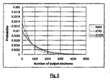
- Figure 5 shows plots of this formula for three different EM gains.
- the y-axis plots probability and the x-axis is the number of output electrons, x, arising from a single input electron.
- the number of electrons is an integer and so Figure 5 is really a histogram with an area of unity.
- a dark image (which in this case comprises a full resolution image readout in the dark) from an EMCCD with a high EM gain (e.g. approximately X1000)
- the single events appear as randomly distributed spikes in the output signal 29 and are readily distinguishable from the readout noise floor.
- a threshold level may be set and any spike protruding above this threshold is counted as a single event and its height above the noise floor is measured (conveniently in electrons),
- the threshold needs to be set high enough so as not to mistake readout noise spikes as events, but not so high that insufficient events will be counted. Therefore, it is recommended to use three standard deviations of the noise floor, which is 180 electrons for this CCD device. Events are thus measured and Equation 4 is fitted to the characteristics of the measured events in order to determine EM gain.
- equation [5] can be solved for G + equal to 1005 and G - equal to 995; this yields approximately 8500 events.
- G + equal to 1005
- G - equal to 995
- this would take well under 1 second to accumulate.
- overscan is employed and a very restricting case of only 1 overscan row per image is assumed, then it will take approximately 4 minutes to acquire enough statistics/data from output events to determine the EM gain. Since the apparatus/camera can still be used while these events are being acquired this need not be a problem at all.
Landscapes
- Engineering & Computer Science (AREA)
- Multimedia (AREA)
- Signal Processing (AREA)
- Health & Medical Sciences (AREA)
- Biomedical Technology (AREA)
- General Health & Medical Sciences (AREA)
- Transforming Light Signals Into Electric Signals (AREA)
- Solid State Image Pick-Up Elements (AREA)
- Photometry And Measurement Of Optical Pulse Characteristics (AREA)
- Analysing Materials By The Use Of Radiation (AREA)
Applications Claiming Priority (1)
| Application Number | Priority Date | Filing Date | Title |
|---|---|---|---|
| GBGB0501149.9A GB0501149D0 (en) | 2005-01-20 | 2005-01-20 | Automatic calibration of electron multiplying CCds |
Publications (3)
| Publication Number | Publication Date |
|---|---|
| EP1688960A2 EP1688960A2 (en) | 2006-08-09 |
| EP1688960A3 EP1688960A3 (en) | 2008-04-02 |
| EP1688960B1 true EP1688960B1 (en) | 2011-04-06 |
Family
ID=34224874
Family Applications (1)
| Application Number | Title | Priority Date | Filing Date |
|---|---|---|---|
| EP06075126A Active EP1688960B1 (en) | 2005-01-20 | 2006-01-18 | Automatic calibration of electron multiplying CCDs |
Country Status (6)
| Country | Link |
|---|---|
| US (1) | US7609311B2 (enExample) |
| EP (1) | EP1688960B1 (enExample) |
| JP (1) | JP5319872B2 (enExample) |
| AT (1) | ATE504923T1 (enExample) |
| DE (1) | DE602006021080D1 (enExample) |
| GB (1) | GB0501149D0 (enExample) |
Families Citing this family (27)
| Publication number | Priority date | Publication date | Assignee | Title |
|---|---|---|---|---|
| GB2429521A (en) | 2005-08-18 | 2007-02-28 | E2V Tech | CCD device for time resolved spectroscopy |
| GB2431538B (en) * | 2005-10-24 | 2010-12-22 | E2V Tech | CCD device |
| DE102006000976A1 (de) | 2006-01-07 | 2007-07-12 | Leica Microsystems Cms Gmbh | Vorrichtung, Mikroskop mit Vorrichtung und Verfahren zum Kalibrieren eines Photosensor-Chips |
| GB2435126A (en) * | 2006-02-14 | 2007-08-15 | E2V Tech | EMCCD device with multiplication register gain measurement allowing realtime calibration of a camera in use. |
| JP4835836B2 (ja) | 2006-03-30 | 2011-12-14 | 日本電気株式会社 | 電子増倍ゲイン校正機構および電子増倍ゲイン校正方法 |
| JP5290530B2 (ja) | 2007-03-19 | 2013-09-18 | 日本電気株式会社 | 電子増倍型撮像装置 |
| JP2008271049A (ja) * | 2007-04-18 | 2008-11-06 | Hamamatsu Photonics Kk | 撮像装置及びそのゲイン調整方法 |
| JP4851388B2 (ja) * | 2007-05-16 | 2012-01-11 | 浜松ホトニクス株式会社 | 撮像装置 |
| KR100976284B1 (ko) * | 2007-06-07 | 2010-08-16 | 가부시끼가이샤 도시바 | 촬상 장치 |
| GB0717484D0 (en) * | 2007-09-07 | 2007-10-17 | E2V Tech Uk Ltd | Gain measurement method |
| FR2924862B1 (fr) * | 2007-12-10 | 2010-08-13 | Commissariat Energie Atomique | Dispositif microelectronique photosensible avec multiplicateurs par avalanche |
| WO2009102839A2 (en) * | 2008-02-14 | 2009-08-20 | The Research Foundation Of State University Of New York | Imaging array data acquisition system and use thereof |
| EP2272027B1 (en) * | 2008-04-16 | 2014-03-26 | Elbit Systems Ltd. | Multispectral enhanced vision system and method for aircraft landing in inclement weather conditions |
| JP2010161183A (ja) * | 2009-01-07 | 2010-07-22 | Panasonic Corp | 固体撮像装置 |
| JP5243984B2 (ja) | 2009-01-30 | 2013-07-24 | 浜松ホトニクス株式会社 | 電子増倍機能内蔵型の固体撮像素子 |
| US8537260B2 (en) * | 2009-05-08 | 2013-09-17 | Photon Etc, Inc. | Apparatus and method for low noise imaging |
| JP5551510B2 (ja) | 2010-05-14 | 2014-07-16 | 浜松ホトニクス株式会社 | 電子増倍率の測定方法及び撮像装置 |
| JP5547548B2 (ja) | 2010-05-14 | 2014-07-16 | 浜松ホトニクス株式会社 | 電子増倍率の測定方法 |
| CN102158661B (zh) * | 2011-01-26 | 2012-09-19 | 中国科学院长春光学精密机械与物理研究所 | 一种emccd特有信号的驱动系统 |
| US8847285B2 (en) | 2011-09-26 | 2014-09-30 | Semiconductor Components Industries, Llc | Depleted charge-multiplying CCD image sensor |
| JP6267529B2 (ja) * | 2014-02-04 | 2018-01-24 | 株式会社日立ハイテクノロジーズ | 荷電粒子線装置及び画像生成方法 |
| GB201516701D0 (en) * | 2015-09-21 | 2015-11-04 | Innovation & Business Dev Solutions Ltd | Time of flight distance sensor |
| US9930276B2 (en) | 2016-01-14 | 2018-03-27 | Semiconductor Components Industries, Llc | Methods for clocking an image sensor |
| US9905608B1 (en) | 2017-01-11 | 2018-02-27 | Semiconductor Components Industries, Llc | EMCCD image sensor with stable charge multiplication gain |
| GB201704452D0 (en) | 2017-03-21 | 2017-05-03 | Photonic Vision Ltd | Time of flight sensor |
| CN110996095B (zh) * | 2019-12-03 | 2021-09-14 | 哈尔滨工程大学 | 一种倍增ccd倍增增益拟合测量方法 |
| CN111988546B (zh) * | 2020-09-15 | 2023-03-31 | 哈尔滨工程大学 | 一种倍增ccd倍增增益及读出噪声测量方法 |
Family Cites Families (12)
| Publication number | Priority date | Publication date | Assignee | Title |
|---|---|---|---|---|
| US3898452A (en) * | 1974-08-15 | 1975-08-05 | Itt | Electron multiplier gain stabilization |
| JP2867655B2 (ja) * | 1990-08-09 | 1999-03-08 | ソニー株式会社 | 固体撮像素子 |
| EP0526993B1 (en) * | 1991-07-11 | 2000-09-27 | Texas Instruments Incorporated | Charge multiplying detector (CMD) suitable for small pixel CCD image sensors |
| JP3221103B2 (ja) * | 1992-10-13 | 2001-10-22 | ソニー株式会社 | 固体撮像装置 |
| GB2323471B (en) * | 1997-03-22 | 2002-04-17 | Eev Ltd | CCd imagers |
| GB9828166D0 (en) * | 1998-12-22 | 1999-02-17 | Eev Ltd | Imaging apparatus |
| DE60021679T2 (de) * | 1999-05-18 | 2006-06-08 | Olympus Corporation | Endoskop |
| US7420605B2 (en) * | 2001-01-18 | 2008-09-02 | E2V Technologies (Uk) Limited | Solid state imager arrangements |
| JP2003009000A (ja) * | 2001-06-21 | 2003-01-10 | Fuji Photo Film Co Ltd | 撮像装置 |
| US6784412B2 (en) * | 2001-08-29 | 2004-08-31 | Texas Instruments Incorporated | Compact image sensor layout with charge multiplying register |
| JP2005005512A (ja) * | 2003-06-12 | 2005-01-06 | Matsushita Electric Ind Co Ltd | 固体撮像装置 |
| US7078670B2 (en) * | 2003-09-15 | 2006-07-18 | Imagerlabs, Inc. | Low noise charge gain circuit and CCD using same |
-
2005
- 2005-01-20 GB GBGB0501149.9A patent/GB0501149D0/en not_active Ceased
-
2006
- 2006-01-18 DE DE602006021080T patent/DE602006021080D1/de active Active
- 2006-01-18 EP EP06075126A patent/EP1688960B1/en active Active
- 2006-01-18 AT AT06075126T patent/ATE504923T1/de not_active IP Right Cessation
- 2006-01-19 US US11/335,889 patent/US7609311B2/en active Active
- 2006-01-20 JP JP2006039971A patent/JP5319872B2/ja not_active Expired - Fee Related
Also Published As
| Publication number | Publication date |
|---|---|
| EP1688960A2 (en) | 2006-08-09 |
| JP5319872B2 (ja) | 2013-10-16 |
| GB0501149D0 (en) | 2005-02-23 |
| ATE504923T1 (de) | 2011-04-15 |
| JP2006203222A (ja) | 2006-08-03 |
| EP1688960A3 (en) | 2008-04-02 |
| US20060163474A1 (en) | 2006-07-27 |
| DE602006021080D1 (de) | 2011-05-19 |
| US7609311B2 (en) | 2009-10-27 |
Similar Documents
| Publication | Publication Date | Title |
|---|---|---|
| EP1688960B1 (en) | Automatic calibration of electron multiplying CCDs | |
| US8054363B2 (en) | Determining the multiplication of EMCCD sensor | |
| KR100962002B1 (ko) | 카드뮴-텔루르계 및 카드뮴-아연-텔루르계 카메라용고에너지 실시간 직접 방사선 변환 엑스선 이미징 시스템 | |
| CA1103346A (en) | Methods of operating imagers | |
| US7807952B2 (en) | Gain calibration in EMCCD cameras | |
| US8004579B2 (en) | Gain measurement structure | |
| EP1159760B1 (en) | Optical test structure for measuring charge-transfer efficiency | |
| DE3501407C2 (de) | Anordnung zur Regelung des Dunkelstroms in Festkörperbauelementen | |
| Pain et al. | An enhanced-performance CMOS imager with a flushed-reset photodiode pixel | |
| GB2105035A (en) | Instrument for measuring light emission | |
| Greffe et al. | Characterization of low light performance of a CMOS Sensor for ultraviolet astronomical applications | |
| US7633068B2 (en) | Count uniformity correction in flux space for pixilated semiconducting radiation detectors | |
| US20050007473A1 (en) | Reducing image sensor lag | |
| US20100141263A1 (en) | System and method for testing an image sensor using gradation image capture | |
| JP2008524874A (ja) | Cd−TeおよびCd−Zn−Teベースカメラ用の高エネルギーの実時間可能な直接放射線変換X線撮像システム | |
| Lumb et al. | Energy and time response of CCD X-ray detectors | |
| US5157501A (en) | Blooming measuring method for solid state image pick-up device, and apparatus suitable for the measuring | |
| US20050128330A1 (en) | Solid-state image sensing device | |
| US7385637B2 (en) | Method for determining image sensor reference image | |
| Janesick | DN to [lambda] | |
| Turko et al. | Gamma ray spectrometer readout with linear CCD sensor | |
| Baril et al. | Characterization of persistence in WIRCam's Hawaii 2-RG arrays | |
| Welsch et al. | Operational experience with a CID camera system | |
| Jammer | Silicon Photomultipliers for UHECR Observation from Space | |
| Pinheiro da Silva et al. | Photometric Calibration |
Legal Events
| Date | Code | Title | Description |
|---|---|---|---|
| PUAI | Public reference made under article 153(3) epc to a published international application that has entered the european phase |
Free format text: ORIGINAL CODE: 0009012 |
|
| AK | Designated contracting states |
Kind code of ref document: A2 Designated state(s): AT BE BG CH CY CZ DE DK EE ES FI FR GB GR HU IE IS IT LI LT LU LV MC NL PL PT RO SE SI SK TR |
|
| AX | Request for extension of the european patent |
Extension state: AL BA HR MK YU |
|
| PUAL | Search report despatched |
Free format text: ORIGINAL CODE: 0009013 |
|
| AK | Designated contracting states |
Kind code of ref document: A3 Designated state(s): AT BE BG CH CY CZ DE DK EE ES FI FR GB GR HU IE IS IT LI LT LU LV MC NL PL PT RO SE SI SK TR |
|
| AX | Request for extension of the european patent |
Extension state: AL BA HR MK YU |
|
| 17P | Request for examination filed |
Effective date: 20080929 |
|
| AKX | Designation fees paid |
Designated state(s): AT BE BG CH CY CZ DE DK EE ES FI FR GB GR HU IE IS IT LI LT LU LV MC NL PL PT RO SE SI SK TR |
|
| 17Q | First examination report despatched |
Effective date: 20081211 |
|
| GRAP | Despatch of communication of intention to grant a patent |
Free format text: ORIGINAL CODE: EPIDOSNIGR1 |
|
| RTI1 | Title (correction) |
Free format text: AUTOMATIC CALIBRATION OF ELECTRON MULTIPLYING CCDS |
|
| GRAS | Grant fee paid |
Free format text: ORIGINAL CODE: EPIDOSNIGR3 |
|
| GRAA | (expected) grant |
Free format text: ORIGINAL CODE: 0009210 |
|
| AK | Designated contracting states |
Kind code of ref document: B1 Designated state(s): AT BE BG CH CY CZ DE DK EE ES FI FR GB GR HU IE IS IT LI LT LU LV MC NL PL PT RO SE SI SK TR |
|
| REG | Reference to a national code |
Ref country code: GB Ref legal event code: FG4D |
|
| REG | Reference to a national code |
Ref country code: CH Ref legal event code: EP |
|
| REG | Reference to a national code |
Ref country code: IE Ref legal event code: FG4D |
|
| REF | Corresponds to: |
Ref document number: 602006021080 Country of ref document: DE Date of ref document: 20110519 Kind code of ref document: P |
|
| REG | Reference to a national code |
Ref country code: DE Ref legal event code: R096 Ref document number: 602006021080 Country of ref document: DE Effective date: 20110519 |
|
| REG | Reference to a national code |
Ref country code: NL Ref legal event code: VDEP Effective date: 20110406 |
|
| PG25 | Lapsed in a contracting state [announced via postgrant information from national office to epo] |
Ref country code: SI Free format text: LAPSE BECAUSE OF FAILURE TO SUBMIT A TRANSLATION OF THE DESCRIPTION OR TO PAY THE FEE WITHIN THE PRESCRIBED TIME-LIMIT Effective date: 20110406 |
|
| LTIE | Lt: invalidation of european patent or patent extension |
Effective date: 20110406 |
|
| PG25 | Lapsed in a contracting state [announced via postgrant information from national office to epo] |
Ref country code: SE Free format text: LAPSE BECAUSE OF FAILURE TO SUBMIT A TRANSLATION OF THE DESCRIPTION OR TO PAY THE FEE WITHIN THE PRESCRIBED TIME-LIMIT Effective date: 20110406 Ref country code: PT Free format text: LAPSE BECAUSE OF FAILURE TO SUBMIT A TRANSLATION OF THE DESCRIPTION OR TO PAY THE FEE WITHIN THE PRESCRIBED TIME-LIMIT Effective date: 20110808 Ref country code: LT Free format text: LAPSE BECAUSE OF FAILURE TO SUBMIT A TRANSLATION OF THE DESCRIPTION OR TO PAY THE FEE WITHIN THE PRESCRIBED TIME-LIMIT Effective date: 20110406 |
|
| PG25 | Lapsed in a contracting state [announced via postgrant information from national office to epo] |
Ref country code: IS Free format text: LAPSE BECAUSE OF FAILURE TO SUBMIT A TRANSLATION OF THE DESCRIPTION OR TO PAY THE FEE WITHIN THE PRESCRIBED TIME-LIMIT Effective date: 20110806 Ref country code: CY Free format text: LAPSE BECAUSE OF FAILURE TO SUBMIT A TRANSLATION OF THE DESCRIPTION OR TO PAY THE FEE WITHIN THE PRESCRIBED TIME-LIMIT Effective date: 20110406 Ref country code: GR Free format text: LAPSE BECAUSE OF FAILURE TO SUBMIT A TRANSLATION OF THE DESCRIPTION OR TO PAY THE FEE WITHIN THE PRESCRIBED TIME-LIMIT Effective date: 20110707 Ref country code: BE Free format text: LAPSE BECAUSE OF FAILURE TO SUBMIT A TRANSLATION OF THE DESCRIPTION OR TO PAY THE FEE WITHIN THE PRESCRIBED TIME-LIMIT Effective date: 20110406 Ref country code: LV Free format text: LAPSE BECAUSE OF FAILURE TO SUBMIT A TRANSLATION OF THE DESCRIPTION OR TO PAY THE FEE WITHIN THE PRESCRIBED TIME-LIMIT Effective date: 20110406 Ref country code: FI Free format text: LAPSE BECAUSE OF FAILURE TO SUBMIT A TRANSLATION OF THE DESCRIPTION OR TO PAY THE FEE WITHIN THE PRESCRIBED TIME-LIMIT Effective date: 20110406 Ref country code: AT Free format text: LAPSE BECAUSE OF FAILURE TO SUBMIT A TRANSLATION OF THE DESCRIPTION OR TO PAY THE FEE WITHIN THE PRESCRIBED TIME-LIMIT Effective date: 20110406 Ref country code: ES Free format text: LAPSE BECAUSE OF FAILURE TO SUBMIT A TRANSLATION OF THE DESCRIPTION OR TO PAY THE FEE WITHIN THE PRESCRIBED TIME-LIMIT Effective date: 20110717 |
|
| PG25 | Lapsed in a contracting state [announced via postgrant information from national office to epo] |
Ref country code: NL Free format text: LAPSE BECAUSE OF FAILURE TO SUBMIT A TRANSLATION OF THE DESCRIPTION OR TO PAY THE FEE WITHIN THE PRESCRIBED TIME-LIMIT Effective date: 20110406 |
|
| PG25 | Lapsed in a contracting state [announced via postgrant information from national office to epo] |
Ref country code: CZ Free format text: LAPSE BECAUSE OF FAILURE TO SUBMIT A TRANSLATION OF THE DESCRIPTION OR TO PAY THE FEE WITHIN THE PRESCRIBED TIME-LIMIT Effective date: 20110406 Ref country code: EE Free format text: LAPSE BECAUSE OF FAILURE TO SUBMIT A TRANSLATION OF THE DESCRIPTION OR TO PAY THE FEE WITHIN THE PRESCRIBED TIME-LIMIT Effective date: 20110406 |
|
| PLBE | No opposition filed within time limit |
Free format text: ORIGINAL CODE: 0009261 |
|
| STAA | Information on the status of an ep patent application or granted ep patent |
Free format text: STATUS: NO OPPOSITION FILED WITHIN TIME LIMIT |
|
| PG25 | Lapsed in a contracting state [announced via postgrant information from national office to epo] |
Ref country code: RO Free format text: LAPSE BECAUSE OF FAILURE TO SUBMIT A TRANSLATION OF THE DESCRIPTION OR TO PAY THE FEE WITHIN THE PRESCRIBED TIME-LIMIT Effective date: 20110406 Ref country code: SK Free format text: LAPSE BECAUSE OF FAILURE TO SUBMIT A TRANSLATION OF THE DESCRIPTION OR TO PAY THE FEE WITHIN THE PRESCRIBED TIME-LIMIT Effective date: 20110406 Ref country code: DK Free format text: LAPSE BECAUSE OF FAILURE TO SUBMIT A TRANSLATION OF THE DESCRIPTION OR TO PAY THE FEE WITHIN THE PRESCRIBED TIME-LIMIT Effective date: 20110406 Ref country code: PL Free format text: LAPSE BECAUSE OF FAILURE TO SUBMIT A TRANSLATION OF THE DESCRIPTION OR TO PAY THE FEE WITHIN THE PRESCRIBED TIME-LIMIT Effective date: 20110406 |
|
| 26N | No opposition filed |
Effective date: 20120110 |
|
| REG | Reference to a national code |
Ref country code: DE Ref legal event code: R097 Ref document number: 602006021080 Country of ref document: DE Effective date: 20120110 |
|
| PG25 | Lapsed in a contracting state [announced via postgrant information from national office to epo] |
Ref country code: MC Free format text: LAPSE BECAUSE OF NON-PAYMENT OF DUE FEES Effective date: 20120131 |
|
| REG | Reference to a national code |
Ref country code: CH Ref legal event code: PL |
|
| REG | Reference to a national code |
Ref country code: IE Ref legal event code: MM4A |
|
| PG25 | Lapsed in a contracting state [announced via postgrant information from national office to epo] |
Ref country code: CH Free format text: LAPSE BECAUSE OF NON-PAYMENT OF DUE FEES Effective date: 20120131 Ref country code: LI Free format text: LAPSE BECAUSE OF NON-PAYMENT OF DUE FEES Effective date: 20120131 |
|
| PG25 | Lapsed in a contracting state [announced via postgrant information from national office to epo] |
Ref country code: IE Free format text: LAPSE BECAUSE OF NON-PAYMENT OF DUE FEES Effective date: 20120118 |
|
| PG25 | Lapsed in a contracting state [announced via postgrant information from national office to epo] |
Ref country code: BG Free format text: LAPSE BECAUSE OF FAILURE TO SUBMIT A TRANSLATION OF THE DESCRIPTION OR TO PAY THE FEE WITHIN THE PRESCRIBED TIME-LIMIT Effective date: 20110706 |
|
| PG25 | Lapsed in a contracting state [announced via postgrant information from national office to epo] |
Ref country code: TR Free format text: LAPSE BECAUSE OF FAILURE TO SUBMIT A TRANSLATION OF THE DESCRIPTION OR TO PAY THE FEE WITHIN THE PRESCRIBED TIME-LIMIT Effective date: 20110406 |
|
| PG25 | Lapsed in a contracting state [announced via postgrant information from national office to epo] |
Ref country code: LU Free format text: LAPSE BECAUSE OF NON-PAYMENT OF DUE FEES Effective date: 20120118 |
|
| PG25 | Lapsed in a contracting state [announced via postgrant information from national office to epo] |
Ref country code: IT Free format text: LAPSE BECAUSE OF FAILURE TO SUBMIT A TRANSLATION OF THE DESCRIPTION OR TO PAY THE FEE WITHIN THE PRESCRIBED TIME-LIMIT Effective date: 20110406 Ref country code: HU Free format text: LAPSE BECAUSE OF FAILURE TO SUBMIT A TRANSLATION OF THE DESCRIPTION OR TO PAY THE FEE WITHIN THE PRESCRIBED TIME-LIMIT Effective date: 20060118 |
|
| REG | Reference to a national code |
Ref country code: FR Ref legal event code: PLFP Year of fee payment: 11 |
|
| REG | Reference to a national code |
Ref country code: FR Ref legal event code: PLFP Year of fee payment: 12 |
|
| REG | Reference to a national code |
Ref country code: FR Ref legal event code: PLFP Year of fee payment: 13 |
|
| PGFP | Annual fee paid to national office [announced via postgrant information from national office to epo] |
Ref country code: GB Payment date: 20221108 Year of fee payment: 18 |
|
| PGFP | Annual fee paid to national office [announced via postgrant information from national office to epo] |
Ref country code: FR Payment date: 20230124 Year of fee payment: 18 |
|
| GBPC | Gb: european patent ceased through non-payment of renewal fee |
Effective date: 20240118 |
|
| PG25 | Lapsed in a contracting state [announced via postgrant information from national office to epo] |
Ref country code: GB Free format text: LAPSE BECAUSE OF NON-PAYMENT OF DUE FEES Effective date: 20240118 |
|
| PG25 | Lapsed in a contracting state [announced via postgrant information from national office to epo] |
Ref country code: FR Free format text: LAPSE BECAUSE OF NON-PAYMENT OF DUE FEES Effective date: 20240131 |
|
| PG25 | Lapsed in a contracting state [announced via postgrant information from national office to epo] |
Ref country code: GB Free format text: LAPSE BECAUSE OF NON-PAYMENT OF DUE FEES Effective date: 20240118 Ref country code: FR Free format text: LAPSE BECAUSE OF NON-PAYMENT OF DUE FEES Effective date: 20240131 |
|
| PGFP | Annual fee paid to national office [announced via postgrant information from national office to epo] |
Ref country code: DE Payment date: 20250121 Year of fee payment: 20 |