EP1685962A2 - Liquid-jet head and liquid-jet apparatus - Google Patents
Liquid-jet head and liquid-jet apparatus Download PDFInfo
- Publication number
- EP1685962A2 EP1685962A2 EP20060250339 EP06250339A EP1685962A2 EP 1685962 A2 EP1685962 A2 EP 1685962A2 EP 20060250339 EP20060250339 EP 20060250339 EP 06250339 A EP06250339 A EP 06250339A EP 1685962 A2 EP1685962 A2 EP 1685962A2
- Authority
- EP
- European Patent Office
- Prior art keywords
- electrode
- lead
- piezoelectric elements
- layer
- liquid
- Prior art date
- Legal status (The legal status is an assumption and is not a legal conclusion. Google has not performed a legal analysis and makes no representation as to the accuracy of the status listed.)
- Withdrawn
Links
- 238000009413 insulation Methods 0.000 claims abstract description 78
- 239000000758 substrate Substances 0.000 claims abstract description 51
- 238000009751 slip forming Methods 0.000 claims abstract description 4
- 239000012774 insulation material Substances 0.000 claims description 13
- TWNQGVIAIRXVLR-UHFFFAOYSA-N oxo(oxoalumanyloxy)alumane Chemical compound O=[Al]O[Al]=O TWNQGVIAIRXVLR-UHFFFAOYSA-N 0.000 claims description 8
- 239000010410 layer Substances 0.000 description 183
- 230000001681 protective effect Effects 0.000 description 21
- 239000000463 material Substances 0.000 description 17
- 238000004519 manufacturing process Methods 0.000 description 15
- 238000000034 method Methods 0.000 description 11
- 239000010931 gold Substances 0.000 description 8
- 239000007788 liquid Substances 0.000 description 8
- PXHVJJICTQNCMI-UHFFFAOYSA-N Nickel Chemical compound [Ni] PXHVJJICTQNCMI-UHFFFAOYSA-N 0.000 description 6
- VYPSYNLAJGMNEJ-UHFFFAOYSA-N Silicium dioxide Chemical compound O=[Si]=O VYPSYNLAJGMNEJ-UHFFFAOYSA-N 0.000 description 6
- 230000007797 corrosion Effects 0.000 description 6
- 238000005260 corrosion Methods 0.000 description 6
- 230000003247 decreasing effect Effects 0.000 description 6
- 229910004243 O3-PbTiO3 Inorganic materials 0.000 description 5
- 229910004293 O3—PbTiO3 Inorganic materials 0.000 description 5
- 229910052782 aluminium Inorganic materials 0.000 description 5
- XAGFODPZIPBFFR-UHFFFAOYSA-N aluminium Chemical compound [Al] XAGFODPZIPBFFR-UHFFFAOYSA-N 0.000 description 5
- 229910052451 lead zirconate titanate Inorganic materials 0.000 description 5
- 239000010955 niobium Substances 0.000 description 5
- 238000007789 sealing Methods 0.000 description 5
- 229910018487 Ni—Cr Inorganic materials 0.000 description 4
- 229910003781 PbTiO3 Inorganic materials 0.000 description 4
- VNNRSPGTAMTISX-UHFFFAOYSA-N chromium nickel Chemical compound [Cr].[Ni] VNNRSPGTAMTISX-UHFFFAOYSA-N 0.000 description 4
- 230000006378 damage Effects 0.000 description 4
- PCHJSUWPFVWCPO-UHFFFAOYSA-N gold Chemical compound [Au] PCHJSUWPFVWCPO-UHFFFAOYSA-N 0.000 description 4
- 229910052737 gold Inorganic materials 0.000 description 4
- 230000008569 process Effects 0.000 description 4
- XUIMIQQOPSSXEZ-UHFFFAOYSA-N Silicon Chemical compound [Si] XUIMIQQOPSSXEZ-UHFFFAOYSA-N 0.000 description 3
- 238000009792 diffusion process Methods 0.000 description 3
- 238000006073 displacement reaction Methods 0.000 description 3
- 229910052751 metal Inorganic materials 0.000 description 3
- 239000002184 metal Substances 0.000 description 3
- 230000004048 modification Effects 0.000 description 3
- 238000012986 modification Methods 0.000 description 3
- 229910021421 monocrystalline silicon Inorganic materials 0.000 description 3
- 229910052710 silicon Inorganic materials 0.000 description 3
- 239000010703 silicon Substances 0.000 description 3
- 235000012239 silicon dioxide Nutrition 0.000 description 3
- 239000000377 silicon dioxide Substances 0.000 description 3
- MAKDTFFYCIMFQP-UHFFFAOYSA-N titanium tungsten Chemical compound [Ti].[W] MAKDTFFYCIMFQP-UHFFFAOYSA-N 0.000 description 3
- 229910020215 Pb(Mg1/3Nb2/3)O3PbTiO3 Inorganic materials 0.000 description 2
- 229910020698 PbZrO3 Inorganic materials 0.000 description 2
- 239000004734 Polyphenylene sulfide Substances 0.000 description 2
- 229910052581 Si3N4 Inorganic materials 0.000 description 2
- 239000000853 adhesive Substances 0.000 description 2
- 230000015572 biosynthetic process Effects 0.000 description 2
- 239000011651 chromium Substances 0.000 description 2
- 238000004891 communication Methods 0.000 description 2
- 239000010949 copper Substances 0.000 description 2
- 229910052741 iridium Inorganic materials 0.000 description 2
- GKOZUEZYRPOHIO-UHFFFAOYSA-N iridium atom Chemical compound [Ir] GKOZUEZYRPOHIO-UHFFFAOYSA-N 0.000 description 2
- 238000005304 joining Methods 0.000 description 2
- HFGPZNIAWCZYJU-UHFFFAOYSA-N lead zirconate titanate Chemical compound [O-2].[O-2].[O-2].[O-2].[O-2].[Ti+4].[Zr+4].[Pb+2] HFGPZNIAWCZYJU-UHFFFAOYSA-N 0.000 description 2
- 238000001459 lithography Methods 0.000 description 2
- 239000000203 mixture Substances 0.000 description 2
- 229910052759 nickel Inorganic materials 0.000 description 2
- BPUBBGLMJRNUCC-UHFFFAOYSA-N oxygen(2-);tantalum(5+) Chemical compound [O-2].[O-2].[O-2].[O-2].[O-2].[Ta+5].[Ta+5] BPUBBGLMJRNUCC-UHFFFAOYSA-N 0.000 description 2
- RVTZCBVAJQQJTK-UHFFFAOYSA-N oxygen(2-);zirconium(4+) Chemical compound [O-2].[O-2].[Zr+4] RVTZCBVAJQQJTK-UHFFFAOYSA-N 0.000 description 2
- 238000000059 patterning Methods 0.000 description 2
- BASFCYQUMIYNBI-UHFFFAOYSA-N platinum Chemical compound [Pt] BASFCYQUMIYNBI-UHFFFAOYSA-N 0.000 description 2
- 229920000069 polyphenylene sulfide Polymers 0.000 description 2
- HQVNEWCFYHHQES-UHFFFAOYSA-N silicon nitride Chemical compound N12[Si]34N5[Si]62N3[Si]51N64 HQVNEWCFYHHQES-UHFFFAOYSA-N 0.000 description 2
- 229910001220 stainless steel Inorganic materials 0.000 description 2
- 239000010935 stainless steel Substances 0.000 description 2
- 229910001936 tantalum oxide Inorganic materials 0.000 description 2
- 239000010936 titanium Substances 0.000 description 2
- 229910001928 zirconium oxide Inorganic materials 0.000 description 2
- VYZAMTAEIAYCRO-UHFFFAOYSA-N Chromium Chemical compound [Cr] VYZAMTAEIAYCRO-UHFFFAOYSA-N 0.000 description 1
- RYGMFSIKBFXOCR-UHFFFAOYSA-N Copper Chemical compound [Cu] RYGMFSIKBFXOCR-UHFFFAOYSA-N 0.000 description 1
- 238000000018 DNA microarray Methods 0.000 description 1
- 244000126211 Hericium coralloides Species 0.000 description 1
- FYYHWMGAXLPEAU-UHFFFAOYSA-N Magnesium Chemical compound [Mg] FYYHWMGAXLPEAU-UHFFFAOYSA-N 0.000 description 1
- 229910020289 Pb(ZrxTi1-x)O3 Inorganic materials 0.000 description 1
- 229910020273 Pb(ZrxTi1−x)O3 Inorganic materials 0.000 description 1
- 239000004642 Polyimide Substances 0.000 description 1
- RTAQQCXQSZGOHL-UHFFFAOYSA-N Titanium Chemical compound [Ti] RTAQQCXQSZGOHL-UHFFFAOYSA-N 0.000 description 1
- 239000002253 acid Substances 0.000 description 1
- 230000004075 alteration Effects 0.000 description 1
- 230000008901 benefit Effects 0.000 description 1
- 229910052797 bismuth Inorganic materials 0.000 description 1
- JCXGWMGPZLAOME-UHFFFAOYSA-N bismuth atom Chemical compound [Bi] JCXGWMGPZLAOME-UHFFFAOYSA-N 0.000 description 1
- 229910010293 ceramic material Inorganic materials 0.000 description 1
- 230000008859 change Effects 0.000 description 1
- 238000006243 chemical reaction Methods 0.000 description 1
- 229910052804 chromium Inorganic materials 0.000 description 1
- 239000004020 conductor Substances 0.000 description 1
- 229910052802 copper Inorganic materials 0.000 description 1
- 238000005520 cutting process Methods 0.000 description 1
- 238000000354 decomposition reaction Methods 0.000 description 1
- 230000007423 decrease Effects 0.000 description 1
- 230000008021 deposition Effects 0.000 description 1
- 238000001312 dry etching Methods 0.000 description 1
- 230000000694 effects Effects 0.000 description 1
- 239000007772 electrode material Substances 0.000 description 1
- 238000005516 engineering process Methods 0.000 description 1
- 238000005530 etching Methods 0.000 description 1
- 239000011521 glass Substances 0.000 description 1
- 239000002241 glass-ceramic Substances 0.000 description 1
- 239000004973 liquid crystal related substance Substances 0.000 description 1
- 229910052749 magnesium Inorganic materials 0.000 description 1
- 239000011777 magnesium Substances 0.000 description 1
- 229910052758 niobium Inorganic materials 0.000 description 1
- GUCVJGMIXFAOAE-UHFFFAOYSA-N niobium atom Chemical compound [Nb] GUCVJGMIXFAOAE-UHFFFAOYSA-N 0.000 description 1
- 239000011368 organic material Substances 0.000 description 1
- 230000002093 peripheral effect Effects 0.000 description 1
- 229910052697 platinum Inorganic materials 0.000 description 1
- 229920001721 polyimide Polymers 0.000 description 1
- 239000002987 primer (paints) Substances 0.000 description 1
- 238000007639 printing Methods 0.000 description 1
- 239000011347 resin Substances 0.000 description 1
- 229920005989 resin Polymers 0.000 description 1
- VSZWPYCFIRKVQL-UHFFFAOYSA-N selanylidenegallium;selenium Chemical compound [Se].[Se]=[Ga].[Se]=[Ga] VSZWPYCFIRKVQL-UHFFFAOYSA-N 0.000 description 1
- 239000002356 single layer Substances 0.000 description 1
- 238000003980 solgel method Methods 0.000 description 1
- 238000000992 sputter etching Methods 0.000 description 1
- 238000006467 substitution reaction Methods 0.000 description 1
- 229910052719 titanium Inorganic materials 0.000 description 1
- XLYOFNOQVPJJNP-UHFFFAOYSA-N water Substances O XLYOFNOQVPJJNP-UHFFFAOYSA-N 0.000 description 1
- 229910052727 yttrium Inorganic materials 0.000 description 1
- VWQVUPCCIRVNHF-UHFFFAOYSA-N yttrium atom Chemical compound [Y] VWQVUPCCIRVNHF-UHFFFAOYSA-N 0.000 description 1
Images






Classifications
-
- B—PERFORMING OPERATIONS; TRANSPORTING
- B41—PRINTING; LINING MACHINES; TYPEWRITERS; STAMPS
- B41J—TYPEWRITERS; SELECTIVE PRINTING MECHANISMS, i.e. MECHANISMS PRINTING OTHERWISE THAN FROM A FORME; CORRECTION OF TYPOGRAPHICAL ERRORS
- B41J2/00—Typewriters or selective printing mechanisms characterised by the printing or marking process for which they are designed
- B41J2/005—Typewriters or selective printing mechanisms characterised by the printing or marking process for which they are designed characterised by bringing liquid or particles selectively into contact with a printing material
- B41J2/01—Ink jet
- B41J2/135—Nozzles
- B41J2/16—Production of nozzles
- B41J2/1607—Production of print heads with piezoelectric elements
- B41J2/161—Production of print heads with piezoelectric elements of film type, deformed by bending and disposed on a diaphragm
-
- B—PERFORMING OPERATIONS; TRANSPORTING
- B41—PRINTING; LINING MACHINES; TYPEWRITERS; STAMPS
- B41J—TYPEWRITERS; SELECTIVE PRINTING MECHANISMS, i.e. MECHANISMS PRINTING OTHERWISE THAN FROM A FORME; CORRECTION OF TYPOGRAPHICAL ERRORS
- B41J2/00—Typewriters or selective printing mechanisms characterised by the printing or marking process for which they are designed
- B41J2/005—Typewriters or selective printing mechanisms characterised by the printing or marking process for which they are designed characterised by bringing liquid or particles selectively into contact with a printing material
- B41J2/01—Ink jet
- B41J2/135—Nozzles
- B41J2/14—Structure thereof only for on-demand ink jet heads
- B41J2/14201—Structure of print heads with piezoelectric elements
- B41J2/14233—Structure of print heads with piezoelectric elements of film type, deformed by bending and disposed on a diaphragm
-
- B—PERFORMING OPERATIONS; TRANSPORTING
- B41—PRINTING; LINING MACHINES; TYPEWRITERS; STAMPS
- B41J—TYPEWRITERS; SELECTIVE PRINTING MECHANISMS, i.e. MECHANISMS PRINTING OTHERWISE THAN FROM A FORME; CORRECTION OF TYPOGRAPHICAL ERRORS
- B41J2/00—Typewriters or selective printing mechanisms characterised by the printing or marking process for which they are designed
- B41J2/005—Typewriters or selective printing mechanisms characterised by the printing or marking process for which they are designed characterised by bringing liquid or particles selectively into contact with a printing material
- B41J2/01—Ink jet
- B41J2/135—Nozzles
- B41J2/16—Production of nozzles
- B41J2/1621—Manufacturing processes
- B41J2/1623—Manufacturing processes bonding and adhesion
-
- B—PERFORMING OPERATIONS; TRANSPORTING
- B41—PRINTING; LINING MACHINES; TYPEWRITERS; STAMPS
- B41J—TYPEWRITERS; SELECTIVE PRINTING MECHANISMS, i.e. MECHANISMS PRINTING OTHERWISE THAN FROM A FORME; CORRECTION OF TYPOGRAPHICAL ERRORS
- B41J2/00—Typewriters or selective printing mechanisms characterised by the printing or marking process for which they are designed
- B41J2/005—Typewriters or selective printing mechanisms characterised by the printing or marking process for which they are designed characterised by bringing liquid or particles selectively into contact with a printing material
- B41J2/01—Ink jet
- B41J2/135—Nozzles
- B41J2/16—Production of nozzles
- B41J2/1621—Manufacturing processes
- B41J2/1626—Manufacturing processes etching
- B41J2/1628—Manufacturing processes etching dry etching
-
- B—PERFORMING OPERATIONS; TRANSPORTING
- B41—PRINTING; LINING MACHINES; TYPEWRITERS; STAMPS
- B41J—TYPEWRITERS; SELECTIVE PRINTING MECHANISMS, i.e. MECHANISMS PRINTING OTHERWISE THAN FROM A FORME; CORRECTION OF TYPOGRAPHICAL ERRORS
- B41J2/00—Typewriters or selective printing mechanisms characterised by the printing or marking process for which they are designed
- B41J2/005—Typewriters or selective printing mechanisms characterised by the printing or marking process for which they are designed characterised by bringing liquid or particles selectively into contact with a printing material
- B41J2/01—Ink jet
- B41J2/135—Nozzles
- B41J2/16—Production of nozzles
- B41J2/1621—Manufacturing processes
- B41J2/1626—Manufacturing processes etching
- B41J2/1629—Manufacturing processes etching wet etching
-
- B—PERFORMING OPERATIONS; TRANSPORTING
- B41—PRINTING; LINING MACHINES; TYPEWRITERS; STAMPS
- B41J—TYPEWRITERS; SELECTIVE PRINTING MECHANISMS, i.e. MECHANISMS PRINTING OTHERWISE THAN FROM A FORME; CORRECTION OF TYPOGRAPHICAL ERRORS
- B41J2/00—Typewriters or selective printing mechanisms characterised by the printing or marking process for which they are designed
- B41J2/005—Typewriters or selective printing mechanisms characterised by the printing or marking process for which they are designed characterised by bringing liquid or particles selectively into contact with a printing material
- B41J2/01—Ink jet
- B41J2/135—Nozzles
- B41J2/16—Production of nozzles
- B41J2/1621—Manufacturing processes
- B41J2/1631—Manufacturing processes photolithography
-
- B—PERFORMING OPERATIONS; TRANSPORTING
- B41—PRINTING; LINING MACHINES; TYPEWRITERS; STAMPS
- B41J—TYPEWRITERS; SELECTIVE PRINTING MECHANISMS, i.e. MECHANISMS PRINTING OTHERWISE THAN FROM A FORME; CORRECTION OF TYPOGRAPHICAL ERRORS
- B41J2/00—Typewriters or selective printing mechanisms characterised by the printing or marking process for which they are designed
- B41J2/005—Typewriters or selective printing mechanisms characterised by the printing or marking process for which they are designed characterised by bringing liquid or particles selectively into contact with a printing material
- B41J2/01—Ink jet
- B41J2/135—Nozzles
- B41J2/16—Production of nozzles
- B41J2/1621—Manufacturing processes
- B41J2/1632—Manufacturing processes machining
-
- B—PERFORMING OPERATIONS; TRANSPORTING
- B41—PRINTING; LINING MACHINES; TYPEWRITERS; STAMPS
- B41J—TYPEWRITERS; SELECTIVE PRINTING MECHANISMS, i.e. MECHANISMS PRINTING OTHERWISE THAN FROM A FORME; CORRECTION OF TYPOGRAPHICAL ERRORS
- B41J2/00—Typewriters or selective printing mechanisms characterised by the printing or marking process for which they are designed
- B41J2/005—Typewriters or selective printing mechanisms characterised by the printing or marking process for which they are designed characterised by bringing liquid or particles selectively into contact with a printing material
- B41J2/01—Ink jet
- B41J2/135—Nozzles
- B41J2/14—Structure thereof only for on-demand ink jet heads
- B41J2/14201—Structure of print heads with piezoelectric elements
- B41J2/14233—Structure of print heads with piezoelectric elements of film type, deformed by bending and disposed on a diaphragm
- B41J2002/14241—Structure of print heads with piezoelectric elements of film type, deformed by bending and disposed on a diaphragm having a cover around the piezoelectric thin film element
-
- B—PERFORMING OPERATIONS; TRANSPORTING
- B41—PRINTING; LINING MACHINES; TYPEWRITERS; STAMPS
- B41J—TYPEWRITERS; SELECTIVE PRINTING MECHANISMS, i.e. MECHANISMS PRINTING OTHERWISE THAN FROM A FORME; CORRECTION OF TYPOGRAPHICAL ERRORS
- B41J2/00—Typewriters or selective printing mechanisms characterised by the printing or marking process for which they are designed
- B41J2/005—Typewriters or selective printing mechanisms characterised by the printing or marking process for which they are designed characterised by bringing liquid or particles selectively into contact with a printing material
- B41J2/01—Ink jet
- B41J2/135—Nozzles
- B41J2/14—Structure thereof only for on-demand ink jet heads
- B41J2002/14419—Manifold
-
- B—PERFORMING OPERATIONS; TRANSPORTING
- B41—PRINTING; LINING MACHINES; TYPEWRITERS; STAMPS
- B41J—TYPEWRITERS; SELECTIVE PRINTING MECHANISMS, i.e. MECHANISMS PRINTING OTHERWISE THAN FROM A FORME; CORRECTION OF TYPOGRAPHICAL ERRORS
- B41J2/00—Typewriters or selective printing mechanisms characterised by the printing or marking process for which they are designed
- B41J2/005—Typewriters or selective printing mechanisms characterised by the printing or marking process for which they are designed characterised by bringing liquid or particles selectively into contact with a printing material
- B41J2/01—Ink jet
- B41J2/135—Nozzles
- B41J2/14—Structure thereof only for on-demand ink jet heads
- B41J2002/14491—Electrical connection
Definitions
- This invention relates to a liquid-jet head and a liquid-jet apparatus in which a part of a pressure generating chamber communicating with a nozzle orifice for ejection of liquid droplets is composed of a vibration plate, a piezoelectric element is formed on the vibration plate, and liquid droplets are ejected by displacement of the piezoelectric element. More particularly, the invention relates to an ink-jet recording head and an ink-jet recording apparatus for ejecting ink as a liquid.
- a part of a pressure generating chamber communicating with a nozzle orifice for ejection of ink droplets is composed of a vibration plate, and the vibration plate is deformed by a piezoelectric element to pressurize ink in the pressure generating chamber, thereby ejecting ink droplets from the nozzle orifice.
- Two types of the ink-jet recording heads are put into practical use. One of them uses a piezoelectric actuator of a longitudinal vibration mode which expands and contracts in the axial direction of the piezoelectric element. The other uses a piezoelectric actuator of a flexural vibration mode.
- the former type can change the volume of the pressure generating chamber by abutting the end surface of the piezoelectric element against the vibration plate, thus making it possible to manufacture a head suitable for high density printing.
- this necessitates a difficult process in which the piezoelectric element is cut and divided in a comb tooth shape coincident with the array pitch of the nozzle orifice, and an operation for aligning and fixing the cut and divided piezoelectric element to the pressure generating chamber.
- the problem arises that the manufacturing process is complicated.
- the piezoelectric element can be fabricated and installed on the vibration plate by a relatively simple process in which a green sheet, as a piezoelectric material, is affixed to the vibration plate in agreement with the shape of the pressure generating chamber, and is then sintered.
- a certain size of vibration plate is required due to the usage of flexural vibration, thus posing the problem that a high density array of the piezoelectric elements is difficult.
- the advantage is obtained that not only the piezoelectric element can be fabricated and installed in high density by the lithography method which is an accurate and simple method, but also the thickness of the piezoelectric element can be rendered small and a high speed drive can be accomplished.
- one of electrodes (i.e., a common electrode) of each piezoelectric element is formed to be common to the plurality of piezoelectric elements.
- a multi-layered electrode layer, a connecting wiring layer, etc. which comprise a conductive material, are provided on a lower electrode film which is the common electrode of the piezoelectric element.
- the multi-layered electrode layer is directly formed on the lower electrode film, as in the structure described in the above patent document, there may be a problem such that stray current corrosion occurs between the lower electrode film and the multi-layered electrode layer in forming the multi-layered electrode layer.
- Such a problem is not limited to the ink-jet recording head for ejecting ink, but also holds true of other liquid-jet heads for ejecting liquid droplets other than ink.
- the present invention has been accomplished in the light of the above-described circumstances. It is an object of the invention to provide a liquid-jet head and a liquid-jet apparatus which can retain satisfactory liquid ejection characteristics and can obtain stable liquid ejection characteristics.
- a first aspect of the present invention for attaining the above object is a liquid-jet head, comprising:
- the resistance value of the lower electrode which is the common electrode, is substantially decreased by the auxiliary electrode layer. Consequently, a drop in voltage when the piezoelectric elements are driven can be prevented, and the liquid ejection characteristics are maintained always satisfactorily. Moreover, the vicinity of the end portion of the auxiliary electrode layer is located on the first insulation film. Thus, stray current corrosion can be prevented from occurring between the auxiliary electrode layer and the lower electrode during the manufacturing process, and the auxiliary electrode layer can be formed in a satisfactory manner.
- a second aspect of the present invention is the liquid-jet head according to the first aspect, characterized in that the auxiliary electrode layer at least includes a first conductive layer comprising layers identical with those of the first lead electrode.
- the resistance value of the lower electrode which is the common electrode, can be reliably decreased by the first conductive layer. Since the first conductive layer is formed from the same layers as the first lead electrode, moreover, the auxiliary electrode layer can be formed without need to increase steps in the manufacturing process.
- a third aspect of the present invention is the liquid-jet head according to the second aspect, characterized in that the lead-out electrode includes a second lead electrode drawn from the first lead electrode, the auxiliary electrode layer includes a second conductive layer comprising layers identical with those of the second lead electrode and provided on the first conductive layer via a second insulation film, the second insulation film has a penetrated portion provided at least in a vicinity of the end portion of the passage-forming substrate in the direction parallel to the arrangement of the piezoelectric elements, and the second conductive layer is in contact with the first conductive layer via the penetrated portion provided in the second insulation film.
- the substantial resistance value of the lower electrode which is the common electrode, is further decreased, whereby a drop in voltage at the time of driving the piezoelectric elements can be more reliably prevented.
- the vicinity of the end portion of the second conductive layer is located on the second insulation film.
- a fourth aspect of the present invention is the liquid-jet head according to the first aspect, characterized in that the lead-out electrode includes the first lead electrode and the second lead electrode drawn from the first lead electrode, and the auxiliary electrode layer is composed of the second conductive layer comprising the layers identical with those of the second lead electrode.
- the substantial resistance value of the lower electrode which is the common electrode, can be reliably decreased by the second conductive layer. Since the second conductive layer is formed from the same layers as the second lead electrode, moreover, the auxiliary electrode layer can be formed without need to increase steps in the manufacturing process.
- a fifth aspect of the present invention is the liquid-jet head according to any one of the first to fourth aspects, characterized in that the first insulation film is continuously provided in a region corresponding to the piezoelectric elements except junctions between the first lead electrodes and the piezoelectric elements.
- the piezoelectric elements are covered with the first insulation film, so that damage to the piezoelectric elements (piezoelectric layer) due to moisture can be prevented.
- a sixth aspect of the present invention is the liquid-jet head according to the fifth aspect, characterized in that the first insulation film comprises an inorganic insulation material.
- the piezoelectric elements can be more reliably protected with the first insulation film.
- a seventh aspect of the present invention is the liquid-jet head according to the third aspect, characterized in that the second insulation film is continuously provided in the region corresponding to the piezoelectric elements except junctions between the first lead electrodes and the second lead electrodes.
- the piezoelectric elements can be covered with the second insulation film, so that damage to the piezoelectric elements (piezoelectric layer) due to moisture can be prevented.
- An eighth aspect of the present invention is the liquid-jet head according to the seventh aspect, characterized in that the second insulation film comprises an inorganic insulation material.
- the piezoelectric elements can be more reliably protected with the second insulation film.
- a ninth aspect of the present invention is the liquid-j et head according to the sixth or eighth aspect, characterized in that the inorganic insulation material is aluminum oxide.
- the piezoelectric elements can be even more reliably protected with the first or second insulation film.
- a tenth aspect of the present invention is the liquid-jet head according to any one of the first to ninth aspects, further comprising a lower electrode lead-out electrode drawn from the lower electrode between the piezoelectric elements adjacent to each other, the lower electrode lead-out electrode being connected to the auxiliary electrode layer.
- the lower electrode lead-out electrode is formed to be continuous with the auxiliary electrode layer, so that the occurrence of a drop in voltage can be more reliably prevented.
- An eleventh aspect of the present invention is a liquid-jet apparatus including the liquid-jet head of any one of the first to tenth aspects.
- a liquid-jet apparatus with enhanced durability and reliability can be achieved.
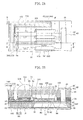
- Fig. 1 is an exploded perspective view showing an ink-jet recording head according to Embodiment 1 of the present invention.
- Fig. 2A is a plan view of the ink-jet recording head in Fig. 1
- Fig. 2B is a sectional view taken on line A-A' of Fig. 2A.
- Fig. 3 is a sectional view taken on line B-B' of Fig. 2A (showing the configuration of electrode layers formed in the vicinity of an end portion of a passage-forming substrate 10 in the direction parallel to the arrangement of a plurality of piezoelectric elements 300) .
- the passage-forming substrate 10 in the present embodiment, consists of a single crystal silicon substratehavingaplane (110) of the plane orientation.
- an elastic film 50 comprising silicon dioxide and having a thickness of 0.5 to 2 ⁇ m is present on one surface of the passage-forming substrate 10.
- a plurality of pressure generating chambers 12 are disposed parallel in the width direction of the passage-forming substrate 10.
- a communicating portion 13 is formed in a region of the passage-forming substrate 10 longitudinally outward of the pressure generating chambers 12.
- the communicating portion 13 and each of the pressure generating chambers 12 are brought into communication via an ink supply path 14 provided for each of the pressure generating chambers 12.
- the communicating portion 13 communicates with a reservoir portion of a protective plate (to be described later) toconstitute a reservoir serving as a common ink chamber for the respective pressure generating chambers 12.
- the ink supply path 14 is formed in a narrower width than that of the pressure generating chamber 12, and keeps constant the passage resistance of ink flowing from the communicating portion 13 into the pressure generating chamber 12.
- a nozzle plate 20 having nozzle orifices 21 bored therein is secured by an adhesive agent or a heat sealing film.
- Each of the nozzle orifices 21 communicates with the vicinity of the end of the pressure generating chamber 12 on the side opposite the ink supply path 14.
- the nozzle plate 20 comprises, for example, a glass ceramic, a single crystal silicon substrate, or stainless steel.
- the elastic film 50 having a thickness, for example, of about 1.0 ⁇ m is formed, as described above.
- a lower electrode film 60 with a thickness, for example, of about 0.2 ⁇ m, a piezoelectric layer 70 with a thickness, for example, of about 1. 0 ⁇ m, and an upper electrode film 80 with a thickness, for example, of about 0.05 ⁇ m are formed in a laminated state by a process (to be described later) to constitute a piezoelectric element 300.
- the piezoelectric element 300 refers to a portion including the lower electrode film 60, the piezoelectric layer 70, and the upper electrode film 80.
- one of the electrodes of the piezoelectric element 300 is used as a common electrode, and the other electrode and the piezoelectric layer 70 are constructed for each pressure generating chamber 12 by patterning.
- the lower electrode film 60 is used as the common electrode for the piezoelectric elements 300
- the upper electrode film 80 is used as an individual electrode of each piezoelectric element 300.
- the piezoelectric active portion is formed for each pressure generating chamber 12.
- the piezoelectric elements 300 and a vibration plate, where displacement is caused by drive of the piezoelectric elements 300 are referred to collectively as a piezoelectric actuator.
- An upper electrode lead-out electrode 90 which extends from the vicinity of an end portion of the pressure generating chamber 12 on the side opposite to the ink supply path 14 to the vicinity of an end portion of the passage-forming substrate 10, is connected to the upper electrode film 80, as the individual electrode, of each piezoelectric element 300.
- the piezoelectric element 300 will be described in detail.
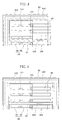
- the lower electrode film 60, as the common electrode, of the piezoelectric element 300 is formed in a region opposite the pressure generating chamber 12 in the longitudinal direction of the pressure generating chamber 12, and is provided continuously over a region corresponding to the plurality of pressure generating chambers 12 in the direction parallel to the arrangement of the pressure generating chambers 12, as shown in Fig. 4.
- the lower electrode film 60 extends to the vicinity of the end portion of the passage-forming substrate 10 in the direction parallel to the arrangement of the pressure generating chambers 12 and, in the present embodiment, is provided continuously so as to surround the periphery of the plurality of upper electrode lead-out electrodes 90, which have been drawn from the respective piezoelectric elements 300.
- the piezoelectric layer 70 and the upper electrode film 80 are basically provided in the region opposite the pressure generating chamber 12, but in the longitudinal direction of the pressure generating chamber 12, extend outwardly from the end portion of the lower electrode film 60, while the end surfaces of the lower electrode film 60 are covered with the piezoelectric layer 70.
- a first insulation film 100 comprising an inorganic insulation material is formed, and the respective layers constituting the piezoelectric element 300 are covered with the first insulation film 100.
- the first insulation film 100 extends to a region where an auxiliary electrode layer 140 (to be described later) is formed.
- the upper electrode lead-out electrode 90 in the present embodiment, includes a first lead electrode 91 connected to the upper electrode film 80, and a second lead electrode 94 connected to the first lead electrode 91.
- the first lead electrode 91 extends onto the first insulation film 100, and is also connected to the upper electrode film 80 via a contact hole 101 formed in the first insulation film 100.
- first lead electrode 91 and the piezoelectric element 300 are further covered with a second insulation film 110 comprising an inorganic insulation material.
- the second insulation film 110 extends to a region where the auxiliary electrode layer 140 is formed, as does the first insulation film.
- the second lead electrode 94 constituting the upper electrode lead-out electrode 90 extends onto the second insulation film 110, and is connected to the first lead electrode 91 via a contact hole 111 formed in the second insulation film 110.
- the first lead electrode 91 in the present embodiment, is composed of an adherence layer 92 with a thickness of the order of 0.1 to 0. 5 ⁇ m, and a metallic layer 93 with a thickness of the order of 0.5 to 3 ⁇ m.
- the material for the adherence layer 92 are nickel (Ni), chromium (Cr), titanium (Ti), copper (Cu), and titanium tungsten (TiW).
- the material for the metallic layer 93 are gold (Au) and aluminum (Al).
- the adherence layer 92 constituting the first lead electrode 91 comprises titanium tungsten (TiW)
- the metallic layer 93 comprises aluminum (Al).
- the second lead electrode 94 is composed of an adherence layer 95 and a metallic layer 96, as is the first lead electrode 91.
- the adherence layer 95 constituting the second lead electrode 94 comprises nickel chromium (NiCr)
- the metallic layer 96 comprises gold (Au).
- the material for the first and second insulation films 100 and 110 is not limited, as long as it is an inorganic insulation material.
- this material are aluminum oxide (AlO x ) and tantalum oxide (TaO x ). Particularly, it is preferred to use an inorganic amorphous material, for example, aluminum oxide (Al 2 O 3 ).
- an organic insulation material such as polyimide.
- the auxiliary electrode layer 140 is provided via the first insulation film 100 and is in contact with the lower electrode film 60.
- the auxiliary electrode layer 140 comprises the same layers as the layers constituting the upper electrode lead-out electrode 90.
- the auxiliary electrode layer 140 includes a first conductive layer 141 comprising the same layers as those of the first lead electrode 91 (i.e., adherence layer 92 and metallic layer 93), and a second conductive layer 142 comprising the same layers as those of the second lead electrode 94 (i.e., adherence layer 95 and metallic layer 96).
- the first insulation film 100 is provided with a penetrated portion 102 in the vicinity of the end portion of the passage-forming substrate 10 in the direction parallel to the arrangement of the piezoelectricelements300.
- the penetrated portion 102 is provided continuously to extend to the vicinity of the end portion of the passage-forming substrate 10 in the longitudinal direction of the piezoelectric elements 300. That is, the penetrated portion 102 is continuously provided so as to surround the periphery of the upper electrode lead-out electrodes 90.
- the first conductive layer 141 is connected to the lower electrode film 60 via the penetrated portion 102 of the first insulation film 100. Also, the penetrated portion 102 in provided in the region opposite the first conductive layer 141. That is, the first conductive layer 141 is formed such that the vicinity of its end portion is located on the first insulation film 100.
- the penetrated portion 102 is formed continuously around the upper electrode lead-out electrodes 90.
- the penetrated portion 102 may, at least, be provided in the first insulation film 100 in the vicinity of the end portion of the passage-forming substrate 10 in the direction parallel to the arrangement of the piezoelectric elements 300, and need not be provided in other regions.
- the second conductive layer 142 is provided on the first conductive layer 141 via the above-mentioned second insulation film 110.
- the second conductive layer 142 and the first conductive layer 141 are connected via a penetrated portion 112 formed in the second insulation film 110 within the region opposite the second conductive layer 142. That is, the second conductive layer 142, like the first conductive layer 141, is formed such that the vicinity of its end portion is located on the second insulation film 110.
- a lower electrode lead-out electrode 97 continued from the first conductive layer 141 is provided in a region between the parallel-arranged piezoelectric elements 300, for example, such that about one lower electrode lead-out electrode 97 is provided for ten of the piezoelectric elements. That is, the lower electrode lead-out electrode 97 is composed of the adherence layer 92 and the metallic layer 93 constituting the first lead electrode 91.
- the lower electrode lead-out electrode 97 is connected to the lower electrode film 60, in a region corresponding to the pressure generating chamber 12 between the adjacent piezoelectric elements 300, via a contact hole 103 provided in the first insulation film 100, and extends along the lead-out direction of the upper electrode lead-out electrode 90.
- the adherence layer 92 constituting the lower electrode lead-out electrode 97, etc. is provided in order to prevent the reaction of the metallic layer 93 comprising aluminum (Al) with the lower electrode film 60, thereby causing mutual diffusion.
- the auxiliary electrode layer 140 consisting of the first conductive layer 141 and the second conductive layer 142 is electrically connected to the lower electrode film 60 which is the common electrode of the piezoelectric element 300.
- the resistance value of the lower electrode film 60 substantially decreases. Consequently, the occurrence of a drop in voltage can be prevented even when many of the piezoelectric elements 300 are simultaneously driven.
- the lower electrode film 60 and the auxiliary electrode layer 140 are brought into conduction via the penetrated portion 102 of a relatively large opening area.
- a plurality of the lower electrode lead-out electrodes 97 are formed to be continuous with the first conductive layer 141 constituting the auxiliary electrode layer 140.
- the penetrated portion 102 in the present embodiment, is provided continuously so as to surround the periphery of the upper electrode lead-out electrodes 90.
- this feature is not limitative, and a plurality of the penetrated portions 102 may be provided around the upper electrode lead-out electrodes 90.
- the plurality of the lower electrode lead-out electrodes 97 are provided, but this is not limitative, and at least one lower electrode lead-out electrode 97 may be provided.
- the lower electrode film 60 is provided continuously around the plurality of upper electrode lead-out electrodes 90 drawn from the respective piezoelectric elements 300.
- the lower electrode film 60 may be provided so as to surround not only the periphery of the upper electrode lead-out electrodes 90, but also the periphery of the respective piezoelectric elements 300.
- the lower electrode film 60 is formed continuously around the upper electrode lead-out electrodes 90, and the auxiliary electrode layer 140 is formed on the lower electrode film 60.
- the auxiliary electrode layer 140 may have a portion thereof formed on the lower electrode film 60 and electrically connected to the lower electrode film 60.
- the lower electrode film 60 may extend, in a predetermined width, only along the direction parallel to the arrangement of the piezoelectric elements 300, and only the auxiliary electrode layer 140 may be continuously formed around the upper electrode lead-out electrodes 90.
- the adhesion of the lower electrode film 60 to the insulation film 55 is weak in some region.
- the insulation film 55 constituting the vibration plate has weak adhesion to the elastic film 50 in some cases.
- the insulation film 55 in regions other than the regions corresponding to the pressure generating chambers 12 may be removed. By so doing, the occurrence of peeling of the insulation film 55 can be minimized.
- the first and second insulation films 100 and 110 comprising the inorganic insulation material, are formed to cover the regions corresponding to the piezoelectric elements 300, so that the piezoelectric elements 300 substantially do not contact the air.
- damage to the piezoelectric elements 300 (piezoelectric layer 70) due to water (moisture) in the air can be prevented.
- the piezoelectric element holding portion 31 may be sealed, but of course, need not be sealed.
- a reservoir portion 32 is provided in a region corresponding to the communicating portion 13 of the passage-forming substrate 10.
- the reservoir portion 32 in the present embodiment, is provided along the direction parallel to the arrangement of the pressure generating chambers 12 so as to penetrate the protective plate 30 in its thickness direction.
- the reservoir portion 32 is brought into communication with the communicating portion 13 of the passage-forming substrate 10 to constitute a reservoir 120 which serves as a common ink chamber for the respective pressure generating chambers 12.
- an exposure hole 33 is formed which penetrates the protective plate 30 in its thickness direction and through which the second lead electrode 94 is exposed.
- the connecting wiring 135 drawn from the drive IC 130 mounted on the protective plate 30 is connected in this exposure hole 33 to the second lead electrode 94 and the second conductive layer 142 (lower electrode film 60).
- the material for the protective plate 30 is, for example, glass, a ceramic material, a metal, or a resin.
- the protective plate 30 is formed of a material having nearly the same thermal expansion coefficient as that of the passage-forming substrate 10.
- the protective plate 30 is formed from a single crystal silicon substrate which is the same material as that for the passage-forming substrate 10.
- a compliance plate 40 which consists of a sealing film 41 and a fixing plate 42, is joined onto the protective plate 30.
- the sealing film 41 comprises a low rigidity, flexible material (for example, a polyphenylene sulfide (PPS) film of 6 ⁇ m in thickness), and the sealing film 41 seals one surface of the reservoir portion 32.
- the fixing plate 42 is formed from a hard material such as a metal (for example, stainless steel (SUS) of 30 ⁇ m in thickness). A region of the fixing plate 42 opposite the reservoir 120 defines an opening portion 43 completely deprived of the plate in the thickness direction. Thus, one surface of the reservoir 120 is sealed only with the sealing film 41 having flexibility.
- ink is taken in from an external ink supply means (not shown) , and the interior of the head ranging from the reservoir 120 to the nozzle orifices 21 is filled with the ink. Then, according to recording signals from the drive IC 130 mounted on the protective plate 30, voltage is applied between the lower electrode film 60 and the upper electrode film 80 corresponding to the pressure generating chamber 12 to flexibly deform the elastic film 50, the insulation film 55, the lower electrode film 60 and the piezoelectric layer 70. As a result, the pressure inside the pressure generating chamber 12 rises to eject ink droplets through the nozzle orifice 21.
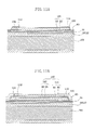
- Figs. 7A to 7D through Figs. 12A to 12C.
- Figs. 7A to 7D, 8A to 8C, 10A to 10C, and 12A to 12C are sectional views corresponding to those taken on line A-A' of Fig. 2A
- Figs. 9A to 9C and 11A and 11B are sectional views corresponding to those taken on line B-B' of Fig. 2A.
- a passage-forming substrate wafer 160 which is a silicon wafer, is thermally oxidized in a diffusion furnace at about 1,100°C to form a silicon dioxide film 52 constituting the elastic film 50 on the surface of the wafer 160.
- a silicon wafer having a relatively large thickness of about 625 ⁇ m and having high rigidity is used as the passage-forming substrate wafer 160 (passage-forming substrate 10).
- a zirconium (Zr) layer is formed on the elastic film 50 (silicon dioxide film 52), and then thermally oxidized in a diffusion furnace, for example, at 500 to 1,200°C to form the insulation film 55 comprising zirconium oxide (ZrO 2 ). Then, as shown in Fig. 7C, platinum and iridium, for example, are stacked on the insulation film 55 to form the lower electrode film 60, whereafter the lower electrode film 60 is patterned into a predetermined shape.
- the piezoelectric layer 70 comprising, for example, lead zirconate titanate (PZT), and the upper electrode film 80 comprising, for example, iridium (Ir) are formed on the entire surface of the passage-forming substrate wafer 160. Then, the piezoelectric layer 70 and the upper electrode film 80 are patterned in a region opposite the respective pressure generating chambers 12 to form the piezoelectric elements 300.
- PZT lead zirconate titanate
- Ir iridium
- the material for the piezoelectric layer 70 may be, for example, a ferroelectric piezoelectric material such as lead zirconate titanate (PZT), or a relaxor ferroelectric having a metal, such as niobium, nickel, magnesium, bismuth or yttrium, added to such a ferroelectric piezoelectric material.
- the composition of the piezoelectric layer 70 may be chosen, as appropriate, in consideration of the characteristics, uses, etc. of the piezoelectric element.
- PbTiO 3 PT
- PbZrO 3 PZ
- Pb(Zr x Ti 1-x )O 3 PZT
- Pb(Mg 1/3 Nb 2/3 )O 3 -PbTiO 3 PMN-PT
- Pb(Zn 1/3 Nb 2/3 )O 3 -PbTiO 3 PZN-PT
- Pb (In 1/2 Nb 1/2 )O 3 -PbTiO 3 (PIN-PT) Pb (Sc 1/3 Ta 2/3 )O 3 -PbTiO 3 (PST-PT)
- Pb (Sc 1/3 Nb 2/3 )O 3 -PbTiO 3 PN-PT
- BiScO 3 -PbTiO 3 BS-PT
- BiYbO 3 -PbTiO 3 BY-PT
- the first insulation film 100 comprising aluminum oxide is formed.
- the first insulation film 100 is etched, for example, via a mask (not shown) comprising a resist or the like, whereby the contact holes 101, 103 and the penetrated portion 102 are formed.
- the first insulation film 100 in regions other than the pattern region of the respective layers constituting the piezoelectric elements 300 is removed.
- the first insulation film 100 may be provided in regions other than the pattern region.
- the method of patterning the first insulation film 100 is not limited, but it is preferred, for example, to use dry etching such as ion milling. By this method, the first insulation film 100 can be selectively removed in a satisfactory manner.
- the first lead electrode 91 is formed, and also the first conductive layer 141 constituting the auxiliary electrode layer 140 and the lower electrode lead-out electrode 97 are formed.
- the adherence layer 92 comprising, for example, titanium tungsten (TiW) is formed on the entire surface of the passage-forming substrate wafer 160, and the metallic layer 93 comprising, for example, aluminum (Al) is formed on the entire surface of the adherence layer 92.
- the metallic layer 93 comprising, for example, aluminum (Al) is formed on the entire surface of the adherence layer 92.
- the metallic layer 93 and the adherence layer 92 are sequentially etched (wet-etched) via a mask (not shown) comprising, for example, a resist to form the first lead electrode 91, the first conductive layer 141 and the lower electrode lead-out electrode 97.
- the first conductive layer 141 is in contact with the lower electrode film 60 via the penetrated portion 102 formed in the first insulation film 100 in the region opposite the first conductive layer 141. That is, the first conductive layer 141 is patterned so that the vicinity of the end portion of the first conductive layer 141 is located on the first insulation film 100. Because of this feature, when the first conductive layer 141 is patterned, no stray current corrosion occurs between the lower electrode film 60 and the first conductive layer 141, and the first conductive layer 141 can be formed satisfactorily.
- the second insulation film 110 comprising aluminum oxide is formed.
- the second insulation film 110 is etched, for example, viaamask (not shown) comprising a resist or the like, whereby the contact hole 111 and the penetrated portion 112 are formed.
- the second insulation film 110 in regions other than the pattern region of the respective layers constituting the piezoelectric elements 300 is removed, as is the first insulation film 100.
- the second lead electrode 94 and the second conductive layer 142 constituting the auxiliary electrode layer 140 are formed.
- the adherence layer 95 comprising, for example, nickel chromium (NiCr) is formed on the entire surface of the passage-forming substrate wafer 160
- the metallic layer 96 comprising, for example, gold (Au) is formed on the entire surface of the adherence layer 95.
- the metallic layer 96 and the adherence layer 95 are sequentially etched via a mask pattern (not shown) to form the second lead electrode 94 and also form the second conductive layer 142 on the second insulation film 110.
- the auxiliary electrode layer 140 consisting of the first conductive layer 142 and the second conductive layer 142 is electrically connected to the lower electrode film 60 via the penetrated portion 102 of the first insulation film 100.
- the second conductive layer 142 is in contact with the first conductive layer 141 via the penetrated portion 112 formed in the second insulation film 110 in the region opposite second conductive layer 142. That is, the second conductive layer 142 is patterned so that the end portion of the second conductive layer 142 is located on the second insulation film 110. Because of this feature, when the second conductive layer 142 is patterned, no stray current corrosion occurs between the first conductive layer 141 and the second conductive layer 142, and the second conductive layer 142 can be formed satisfactorily.
- a protective plate wafer 170 which is a silicon wafer and is to become a plurality of protective plates 30, is joined onto a surface of the passage-forming substrate wafer 160 where the piezoelectric elements 300 have been formed.
- the protective plate wafer 170 has a thickness, for example, of the order of 625 ⁇ m, and thus the rigidity of the passage-forming substrate wafer 160 is markedly increased by joining the protective plate wafer 170 thereto.
- the passage-forming substrate wafer 160 is polished to a certain thickness, and then is wet-etched with fluoronitric acid to bring the passage-forming substrate wafer 160 into a predetermined thickness.
- the passage-forming substrate wafer 160 is processed to have a thickness of about 70 ⁇ m.
- the mask film 51 comprising, for example, silicon nitride (SiN) is formed anew on the passage-forming substrate wafer 160, and is patterned into a predetermined shape.
- the passage-forming substrate wafer 160 is subj ected to anisotropic etching via the mask film 51 to form the pressure generating chambers 12, the communicating portion 13 and the ink supply paths 14 in the passage-forming substrate wafer 160 (Fig. 12C).
- Fig. 13 is a sectional view showing essential parts of an ink-jet recording head according to Embodiment 2, namely, a sectional view corresponding to one taken along line A-A' of Fig. 2A.
- the present embodiment is a modification of the auxiliary electrode layer.
- the auxiliary electrode layer 140 according to Embodiment 1 is composed of a plurality of layers, specifically, the first conductive layer 141 and the second conductive layer 142.
- the auxiliary electrode layer is composed of a single layer. That is, the present embodiment is the same as Embodiment 1, except that an auxiliary electrode layer 140A is composed only of the second conductive layer 142 comprising the same layer as the second lead electrode 94, as shown in Fig. 13.
- Embodiment 1 Even with the above feature, the same effects as in Embodiment 1 are objected. That is, since the resistance value of the lower electrode film 60 is substantially decreased, the occurrence of a drop in voltage can be prevented even when many of the piezoelectric elements 300 are simultaneously driven, as in Embodiment 1. Moreover, when the auxiliary electrode layer 140A (second conductive layer 142) is patterned, no stray current corrosion occurs between the lower electrode film 60 and the auxiliary electrode layer 140A, and the auxiliary electrode layer 140A can be formed satisfactorily.
- the auxiliary electrode layer 140A is composed only of the second conductive layer 142, but it goes without saying that the auxiliary electrode layer 140A may be composed only of the first conductive layer 141 comprising the same layer as the first lead electrode.
- the auxiliary electrode layer 140A is preferably formed from the second conductive layer 142 containing the metallic layer 96 comprising gold (Au). If the auxiliary electrode layer is formed only from the first conductive layer 141 containing the metallic layer 93 comprising, for example, aluminum (A1), the metallic layer 93 is likely to be fused by primer coating performed when joining the passage-forming substrate 10 and the protective plate 30.
- the present invention is not limited to these embodiments.
- the formation of the auxiliary electrode layer composed of the one conductive layer or the two conductive layers (first and second conductive layers) on the lower electrode film is taken as an example.
- the auxiliary electrode layer may be composed of three or more conductive layers.
- Fig. 14 is a schematic view showing an example of this ink-jet recording apparatus.
- cartridges 2A and 2B constituting ink supply means are detachably provided in recording head units 1A and 1B having the ink-j et recording heads, and a carriage 3 bearing the recording head units 1A and 1B is provided axially movably on a carriage shaft 5 mounted on an apparatus body 4.
- the recording head units 1A and 1B are to eject, for example, a black ink composition and a colorinkcomposition,respectively.
- the drive force of a drive motor 6 is transmitted to the carriage 3 via a plurality of gears (not shown) and a timing belt 7, whereby the carriage 3 bearing the recording head units 1A and 1B is moved along the carriage shaft 5.
- the apparatus body 4 is provided with a platen 8 along the carriage shaft 5, and a recording sheet S as a recording medium, such as paper, which has been fed by a sheet feed roller or the like (not shown) is transported on the platen 8.
- the ink-jet recording head is taken for illustration as an example of the liquid-jet head of the present invention.
- the basic configuration of the liquid-jet head is not limited to the above-described one.
- the present invention widely targets liquid-jet heads in general.
- the present invention can be applied to liquid-jet heads for jetting liquids other than ink.
- Other liquid-jet heads include, for example, various recording heads for use in image recording devices such as printers, color material jet heads for use in the production of color filters such as liquid crystal displays, electrode material jet heads for use in the formation of electrodes for organic EL displays and FED (Field Emission Display), and bio-organic material jet heads for use in the production of biochips. It should be understood that such changes, substitutions and alterations can be made therein without departing from the scope of the invention as defined by the appended claims.
Landscapes
- Engineering & Computer Science (AREA)
- Manufacturing & Machinery (AREA)
- Particle Formation And Scattering Control In Inkjet Printers (AREA)
Abstract
Description
- This invention relates to a liquid-jet head and a liquid-jet apparatus in which a part of a pressure generating chamber communicating with a nozzle orifice for ejection of liquid droplets is composed of a vibration plate, a piezoelectric element is formed on the vibration plate, and liquid droplets are ejected by displacement of the piezoelectric element. More particularly, the invention relates to an ink-jet recording head and an ink-jet recording apparatus for ejecting ink as a liquid.
- In an ink-jet recording head, a part of a pressure generating chamber communicating with a nozzle orifice for ejection of ink droplets is composed of a vibration plate, and the vibration plate is deformed by a piezoelectric element to pressurize ink in the pressure generating chamber, thereby ejecting ink droplets from the nozzle orifice. Two types of the ink-jet recording heads are put into practical use. One of them uses a piezoelectric actuator of a longitudinal vibration mode which expands and contracts in the axial direction of the piezoelectric element. The other uses a piezoelectric actuator of a flexural vibration mode.
- The former type can change the volume of the pressure generating chamber by abutting the end surface of the piezoelectric element against the vibration plate, thus making it possible to manufacture a head suitable for high density printing. However, this necessitates a difficult process in which the piezoelectric element is cut and divided in a comb tooth shape coincident with the array pitch of the nozzle orifice, and an operation for aligning and fixing the cut and divided piezoelectric element to the pressure generating chamber. Thus, the problem arises that the manufacturing process is complicated. With the latter type, on the other hand, the piezoelectric element can be fabricated and installed on the vibration plate by a relatively simple process in which a green sheet, as a piezoelectric material, is affixed to the vibration plate in agreement with the shape of the pressure generating chamber, and is then sintered. However, a certain size of vibration plate is required due to the usage of flexural vibration, thus posing the problem that a high density array of the piezoelectric elements is difficult.
- In order to solve the disadvantage of the latter recording head, a proposal has been made for a recording head in which a uniform piezoelectric material layer is formed across the entire surface of the vibration plate by a deposition technology, the piezoelectric material layer is cut and divided into a shape corresponding to the pressure generating chamber by a lithography method, and the piezoelectric element is formed so as to be independent of one another piezoelectric element for each pressure generating chamber. According to this process, the operation for affixing the piezoelectric element to the vibration plate is unnecessary. Moreover, the advantage is obtained that not only the piezoelectric element can be fabricated and installed in high density by the lithography method which is an accurate and simple method, but also the thickness of the piezoelectric element can be rendered small and a high speed drive can be accomplished.
- With the ink-jet recording head having the piezoelectric elements arranged in a high density as described above, one of electrodes (i.e., a common electrode) of each piezoelectric element is formed to be common to the plurality of piezoelectric elements. Thus, when many of the piezoelectric elements are driven at the same time to eject many ink droplets at one time, the problem is presented that a drop in voltage occurs, leading to an unstable amount of displacement of the piezoelectric element and deteriorated ink ejection characteristics. To solve such a problem, a multi-layered electrode layer, a connecting wiring layer, etc., which comprise a conductive material, are provided on a lower electrode film which is the common electrode of the piezoelectric element. By so doing, it is attempted to lower the resistance value of the lower electrode film substantially, thereby preventing the occurrence of a drop in voltage (see, for example, Japanese Patent Application Laid-Open No. 2004-1431).
- However, if the multi-layered electrode layer is directly formed on the lower electrode film, as in the structure described in the above patent document, there may be a problem such that stray current corrosion occurs between the lower electrode film and the multi-layered electrode layer in forming the multi-layered electrode layer.
- Such a problem is not limited to the ink-jet recording head for ejecting ink, but also holds true of other liquid-jet heads for ejecting liquid droplets other than ink.
- The present invention has been accomplished in the light of the above-described circumstances. It is an object of the invention to provide a liquid-jet head and a liquid-jet apparatus which can retain satisfactory liquid ejection characteristics and can obtain stable liquid ejection characteristics.
- A first aspect of the present invention for attaining the above object is a liquid-jet head, comprising:
- a passage-forming substrate in which pressure generating chambers communicating with nozzle orifices are formed;
- piezoelectric elements provided on one surface side of the passage-forming substrate, and each comprising a lower electrode, a piezoelectric layer, and an upper electrode; and
- a lead-out electrode at least including a first lead electrode drawn from each of the piezoelectric elements, and
- wherein the lower electrode, which is a common electrode common to the plurality of piezoelectric elements, is continuously formed as far as an outside of a region opposite the piezoelectric elements,
- an auxiliary electrode layer is provided which comprises layers identical with layers constituting the lead-out electrode, and which is electrically connected to the lower electrode located outwardly of the region opposite the piezoelectric elements,
- a first insulation film covering the piezoelectric elements extends to a region where the auxiliary electrode layer is formed,
- in the first insulation film at least in a vicinity of an end portion of the passage-forming substrate in a direction parallel to the arrangement of the piezoelectric elements, a penetrated portion is provided in a region opposite the auxiliary electrode layer, and
- the auxiliary electrode layer is in contact with the lower electrode via the penetrated portion provided in the first insulation film.
- In the first aspect, the resistance value of the lower electrode, which is the common electrode, is substantially decreased by the auxiliary electrode layer. Consequently, a drop in voltage when the piezoelectric elements are driven can be prevented, and the liquid ejection characteristics are maintained always satisfactorily. Moreover, the vicinity of the end portion of the auxiliary electrode layer is located on the first insulation film. Thus, stray current corrosion can be prevented from occurring between the auxiliary electrode layer and the lower electrode during the manufacturing process, and the auxiliary electrode layer can be formed in a satisfactory manner.
- A second aspect of the present invention is the liquid-jet head according to the first aspect, characterized in that the auxiliary electrode layer at least includes a first conductive layer comprising layers identical with those of the first lead electrode.
- In the second aspect, the resistance value of the lower electrode, which is the common electrode, can be reliably decreased by the first conductive layer. Since the first conductive layer is formed from the same layers as the first lead electrode, moreover, the auxiliary electrode layer can be formed without need to increase steps in the manufacturing process.
- A third aspect of the present invention is the liquid-jet head according to the second aspect, characterized in that the lead-out electrode includes a second lead electrode drawn from the first lead electrode, the auxiliary electrode layer includes a second conductive layer comprising layers identical with those of the second lead electrode and provided on the first conductive layer via a second insulation film, the second insulation film has a penetrated portion provided at least in a vicinity of the end portion of the passage-forming substrate in the direction parallel to the arrangement of the piezoelectric elements, and the second conductive layer is in contact with the first conductive layer via the penetrated portion provided in the second insulation film.
- In the third aspect, the substantial resistance value of the lower electrode, which is the common electrode, is further decreased, whereby a drop in voltage at the time of driving the piezoelectric elements can be more reliably prevented. Furthermore, the vicinity of the end portion of the second conductive layer is located on the second insulation film. Thus, stray current corrosion can be prevented from occurring between the first conductive layer and the second conductive layer during the manufacturing process, and the second conductive layer can be formed in a satisfactory manner.
- A fourth aspect of the present invention is the liquid-jet head according to the first aspect,
characterized in that the lead-out electrode includes the first lead electrode and the second lead electrode drawn from the first lead electrode, and the auxiliary electrode layer is composed of the second conductive layer comprising the layers identical with those of the second lead electrode. - In the fourth aspect, the substantial resistance value of the lower electrode, which is the common electrode, can be reliably decreased by the second conductive layer. Since the second conductive layer is formed from the same layers as the second lead electrode, moreover, the auxiliary electrode layer can be formed without need to increase steps in the manufacturing process.
- A fifth aspect of the present invention is the liquid-jet head according to any one of the first to fourth aspects, characterized in that the first insulation film is continuously provided in a region corresponding to the piezoelectric elements except junctions between the first lead electrodes and the piezoelectric elements.
- In the fifth aspect, the piezoelectric elements are covered with the first insulation film, so that damage to the piezoelectric elements (piezoelectric layer) due to moisture can be prevented.
- A sixth aspect of the present invention is the liquid-jet head according to the fifth aspect,
characterized in that the first insulation film comprises an inorganic insulation material. - In the sixth aspect, the piezoelectric elements can be more reliably protected with the first insulation film.
- A seventh aspect of the present invention is the liquid-jet head according to the third aspect,
characterized in that the second insulation film is continuously provided in the region corresponding to the piezoelectric elements except junctions between the first lead electrodes and the second lead electrodes. - In the seventh aspect, the piezoelectric elements can be covered with the second insulation film, so that damage to the piezoelectric elements (piezoelectric layer) due to moisture can be prevented.
- An eighth aspect of the present invention is the liquid-jet head according to the seventh aspect,
characterized in that the second insulation film comprises an inorganic insulation material. - In the eighth aspect, the piezoelectric elements can be more reliably protected with the second insulation film.
- A ninth aspect of the present invention is the liquid-j et head according to the sixth or eighth aspect,
characterized in that the inorganic insulation material is aluminum oxide. - In the ninth aspect, the piezoelectric elements can be even more reliably protected with the first or second insulation film.
- A tenth aspect of the present invention is the liquid-jet head according to any one of the first to ninth aspects, further comprising a lower electrode lead-out electrode drawn from the lower electrode between the piezoelectric elements adjacent to each other, the lower electrode lead-out electrode being connected to the auxiliary electrode layer.
- In the tenth aspect, the lower electrode lead-out electrode is formed to be continuous with the auxiliary electrode layer, so that the occurrence of a drop in voltage can be more reliably prevented.
- An eleventh aspect of the present invention is a liquid-jet apparatus including the liquid-jet head of any one of the first to tenth aspects.
- In the eleventh aspect, a liquid-jet apparatus with enhanced durability and reliability can be achieved.
- Embodiments of the present invention will now be described by way of further example only and with reference to the accompanying drawings, in which:-
- Fig. 1 is an exploded perspective view of a recording head according to
Embodiment 1. - Figs. 2A and 2B are a plan view and a sectional view, respectively, of the recording head according to
Embodiment 1. - Fig. 3 is a sectional view showing essential parts of the recording head according to
Embodiment 1. - Fig. 4 is a plan view showing the outline of a wiring structure according to
Embodiment 1. - Fig. 5 is a plan view showing a modification of the wiring structure according to
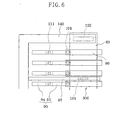
Embodiment 1. - Fig. 6 is a plan view showing a modification of the wiring structure according to
Embodiment 1. - Figs. 7A to 7D are sectional views showing steps in a manufacturing process for the recording head according to
Embodiment 1. - Figs. 8A to 8C are sectional views showing the steps in the manufacturing process for the recording head according to
Embodiment 1. - Figs. 9A to 9C are sectional views showing the steps in the manufacturing process for the recording head according to
Embodiment 1. - Figs. 10A to 10C are sectional views showing the steps in the manufacturing process for the recording head according to
Embodiment 1. - Figs. 11A and 11B are sectional views showing the steps in the manufacturing process for the recording head according to
Embodiment 1. - Figs. 12A to 12C are sectional views showing the steps in the manufacturing process for the recording head according to
Embodiment 1. - Fig. 13 is a sectional view of a recording head according to Embodiment 2.
- Fig. 14 is a schematic view of a recording apparatus according to an embodiment of the present invention.
- The present invention will now be described in detail based on the embodiments offered below.
- Fig. 1 is an exploded perspective view showing an ink-jet recording head according to
Embodiment 1 of the present invention. Fig. 2A is a plan view of the ink-jet recording head in Fig. 1, and Fig. 2B is a sectional view taken on line A-A' of Fig. 2A. Fig. 3 is a sectional view taken on line B-B' of Fig. 2A (showing the configuration of electrode layers formed in the vicinity of an end portion of a passage-formingsubstrate 10 in the direction parallel to the arrangement of a plurality of piezoelectric elements 300) . The passage-formingsubstrate 10, in the present embodiment, consists of a single crystal silicon substratehavingaplane (110) of the plane orientation. As illustrated, anelastic film 50 comprising silicon dioxide and having a thickness of 0.5 to 2 µm is present on one surface of the passage-formingsubstrate 10. In the passage-formingsubstrate 10, a plurality ofpressure generating chambers 12 are disposed parallel in the width direction of the passage-formingsubstrate 10. A communicatingportion 13 is formed in a region of the passage-formingsubstrate 10 longitudinally outward of thepressure generating chambers 12. The communicatingportion 13 and each of thepressure generating chambers 12 are brought into communication via anink supply path 14 provided for each of thepressure generating chambers 12. The communicatingportion 13 communicates with a reservoir portion of a protective plate (to be described later) toconstitute a reservoir serving as a common ink chamber for the respectivepressure generating chambers 12. Theink supply path 14 is formed in a narrower width than that of thepressure generating chamber 12, and keeps constant the passage resistance of ink flowing from the communicatingportion 13 into thepressure generating chamber 12. - Onto an opening surface of the passage-forming
substrate 10, anozzle plate 20 havingnozzle orifices 21 bored therein is secured by an adhesive agent or a heat sealing film. Each of the nozzle orifices 21 communicates with the vicinity of the end of thepressure generating chamber 12 on the side opposite theink supply path 14. Thenozzle plate 20 comprises, for example, a glass ceramic, a single crystal silicon substrate, or stainless steel. - On the surface of the passage-forming
substrate 10 opposite the opening surface, theelastic film 50 having a thickness, for example, of about 1.0 µm is formed, as described above. Aninsulation film 55 having a thickness, for example, of about 0.4 µm is formed on theelastic film 50. On theinsulation film 55, alower electrode film 60 with a thickness, for example, of about 0.2 µm, apiezoelectric layer 70 with a thickness, for example, of about 1. 0 µm, and anupper electrode film 80 with a thickness, for example, of about 0.05 µm are formed in a laminated state by a process (to be described later) to constitute apiezoelectric element 300. Thepiezoelectric element 300 refers to a portion including thelower electrode film 60, thepiezoelectric layer 70, and theupper electrode film 80. Generally, one of the electrodes of thepiezoelectric element 300 is used as a common electrode, and the other electrode and thepiezoelectric layer 70 are constructed for eachpressure generating chamber 12 by patterning. A portion, which is composed of any one of the electrodes and thepiezoelectric layer 70 that have been patterned, and which undergoes piezoelectric distortion upon application of voltage to both electrodes, is called a piezoelectric active portion. In the present embodiment, thelower electrode film 60 is used as the common electrode for thepiezoelectric elements 300, while theupper electrode film 80 is used as an individual electrode of eachpiezoelectric element 300. However, there is no harm in reversing their usages for the convenience of a drive circuit or wiring. In either case, it follows that the piezoelectric active portion is formed for eachpressure generating chamber 12. Herein, thepiezoelectric elements 300 and a vibration plate, where displacement is caused by drive of thepiezoelectric elements 300, are referred to collectively as a piezoelectric actuator. An upper electrode lead-out electrode 90, which extends from the vicinity of an end portion of thepressure generating chamber 12 on the side opposite to theink supply path 14 to the vicinity of an end portion of the passage-formingsubstrate 10, is connected to theupper electrode film 80, as the individual electrode, of eachpiezoelectric element 300. - The
piezoelectric element 300 will be described in detail. Thelower electrode film 60, as the common electrode, of thepiezoelectric element 300 is formed in a region opposite thepressure generating chamber 12 in the longitudinal direction of thepressure generating chamber 12, and is provided continuously over a region corresponding to the plurality ofpressure generating chambers 12 in the direction parallel to the arrangement of thepressure generating chambers 12, as shown in Fig. 4. Thelower electrode film 60 extends to the vicinity of the end portion of the passage-formingsubstrate 10 in the direction parallel to the arrangement of thepressure generating chambers 12 and, in the present embodiment, is provided continuously so as to surround the periphery of the plurality of upper electrode lead-outelectrodes 90, which have been drawn from the respectivepiezoelectric elements 300. - The
piezoelectric layer 70 and theupper electrode film 80 are basically provided in the region opposite thepressure generating chamber 12, but in the longitudinal direction of thepressure generating chamber 12, extend outwardly from the end portion of thelower electrode film 60, while the end surfaces of thelower electrode film 60 are covered with thepiezoelectric layer 70. - In the pattern region of the respective layers constituting the
piezoelectric element 300, afirst insulation film 100 comprising an inorganic insulation material is formed, and the respective layers constituting thepiezoelectric element 300 are covered with thefirst insulation film 100. Thefirst insulation film 100 extends to a region where an auxiliary electrode layer 140 (to be described later) is formed. The upper electrode lead-out electrode 90, in the present embodiment, includes afirst lead electrode 91 connected to theupper electrode film 80, and asecond lead electrode 94 connected to thefirst lead electrode 91. Thefirst lead electrode 91 extends onto thefirst insulation film 100, and is also connected to theupper electrode film 80 via acontact hole 101 formed in thefirst insulation film 100. Therespective layers constituting thefirst lead electrode 91 and thepiezoelectric element 300 are further covered with asecond insulation film 110 comprising an inorganic insulation material. Thesecond insulation film 110 extends to a region where theauxiliary electrode layer 140 is formed, as does the first insulation film. Thesecond lead electrode 94 constituting the upper electrode lead-out electrode 90 extends onto thesecond insulation film 110, and is connected to thefirst lead electrode 91 via acontact hole 111 formed in thesecond insulation film 110. A connectingwiring 135, led out of adrive IC 130 mounted on a protective plate 30 (to be described later), is connected to the vicinity of a front end portion of thesecond lead electrode 94. - The
first lead electrode 91, in the present embodiment, is composed of anadherence layer 92 with a thickness of the order of 0.1 to 0. 5 µm, and ametallic layer 93 with a thickness of the order of 0.5 to 3 µm. Examples of the material for theadherence layer 92 are nickel (Ni), chromium (Cr), titanium (Ti), copper (Cu), and titanium tungsten (TiW). Examples of the material for themetallic layer 93 are gold (Au) and aluminum (Al). In the present embodiment, theadherence layer 92 constituting thefirst lead electrode 91 comprises titanium tungsten (TiW), and themetallic layer 93 comprises aluminum (Al). - The
second lead electrode 94 is composed of anadherence layer 95 and ametallic layer 96, as is thefirst lead electrode 91. In the present embodiment, for example, theadherence layer 95 constituting thesecond lead electrode 94 comprises nickel chromium (NiCr) , and themetallic layer 96 comprises gold (Au). - The material for the first and
second insulation films - On the
lower electrode film 60 in the region outward of the parallel-arrangedpressure generating chambers 12, theauxiliary electrode layer 140 is provided via thefirst insulation film 100 and is in contact with thelower electrode film 60. - The
auxiliary electrode layer 140 comprises the same layers as the layers constituting the upper electrode lead-out electrode 90. In the present embodiment, for example, theauxiliary electrode layer 140 includes a firstconductive layer 141 comprising the same layers as those of the first lead electrode 91 (i.e.,adherence layer 92 and metallic layer 93), and a secondconductive layer 142 comprising the same layers as those of the second lead electrode 94 (i.e.,adherence layer 95 and metallic layer 96). As shown in Fig. 3, thefirst insulation film 100 is provided with a penetratedportion 102 in the vicinity of the end portion of the passage-formingsubstrate 10 in the direction parallel to the arrangement of the piezoelectricelements300. In the present embodiment, the penetratedportion 102 is provided continuously to extend to the vicinity of the end portion of the passage-formingsubstrate 10 in the longitudinal direction of thepiezoelectric elements 300. That is, the penetratedportion 102 is continuously provided so as to surround the periphery of the upper electrode lead-outelectrodes 90. The firstconductive layer 141 is connected to thelower electrode film 60 via the penetratedportion 102 of thefirst insulation film 100. Also, the penetratedportion 102 in provided in the region opposite the firstconductive layer 141. That is, the firstconductive layer 141 is formed such that the vicinity of its end portion is located on thefirst insulation film 100. - In the present embodiment, the penetrated
portion 102 is formed continuously around the upper electrode lead-outelectrodes 90. The penetratedportion 102 may, at least, be provided in thefirst insulation film 100 in the vicinity of the end portion of the passage-formingsubstrate 10 in the direction parallel to the arrangement of thepiezoelectric elements 300, and need not be provided in other regions. - The second
conductive layer 142 is provided on the firstconductive layer 141 via the above-mentionedsecond insulation film 110. The secondconductive layer 142 and the firstconductive layer 141 are connected via a penetratedportion 112 formed in thesecond insulation film 110 within the region opposite the secondconductive layer 142. That is, the secondconductive layer 142, like the firstconductive layer 141, is formed such that the vicinity of its end portion is located on thesecond insulation film 110. - In the present embodiment, a lower electrode lead-
out electrode 97 continued from the firstconductive layer 141 is provided in a region between the parallel-arrangedpiezoelectric elements 300, for example, such that about one lower electrode lead-out electrode 97 is provided for ten of the piezoelectric elements. That is, the lower electrode lead-out electrode 97 is composed of theadherence layer 92 and themetallic layer 93 constituting thefirst lead electrode 91. The lower electrode lead-out electrode 97 is connected to thelower electrode film 60, in a region corresponding to thepressure generating chamber 12 between the adjacentpiezoelectric elements 300, via acontact hole 103 provided in thefirst insulation film 100, and extends along the lead-out direction of the upper electrode lead-out electrode 90. Theadherence layer 92 constituting the lower electrode lead-out electrode 97, etc. is provided in order to prevent the reaction of themetallic layer 93 comprising aluminum (Al) with thelower electrode film 60, thereby causing mutual diffusion. - According to the features of the present embodiment described above, the
auxiliary electrode layer 140 consisting of the firstconductive layer 141 and the secondconductive layer 142 is electrically connected to thelower electrode film 60 which is the common electrode of thepiezoelectric element 300. Thus, the resistance value of thelower electrode film 60 substantially decreases. Consequently, the occurrence of a drop in voltage can be prevented even when many of thepiezoelectric elements 300 are simultaneously driven. In the present embodiment, in particular, thelower electrode film 60 and theauxiliary electrode layer 140 are brought into conduction via the penetratedportion 102 of a relatively large opening area. Moreover, a plurality of the lower electrode lead-outelectrodes 97 are formed to be continuous with the firstconductive layer 141 constituting theauxiliary electrode layer 140. Thus, the occurrence of a drop in voltage can be more reliably prevented. Hence, the ink ejection characteristics, which are always satisfactory and stable, can be obtained, and variations in ink ejection characteristics among the piezoelectric elements can also be decreased. The penetratedportion 102, in the present embodiment, is provided continuously so as to surround the periphery of the upper electrode lead-outelectrodes 90. However, this feature is not limitative, and a plurality of the penetratedportions 102 may be provided around the upper electrode lead-outelectrodes 90. In the present embodiment, moreover, the plurality of the lower electrode lead-outelectrodes 97 are provided, but this is not limitative, and at least one lower electrode lead-out electrode 97 may be provided. - In the present embodiment, the
lower electrode film 60 is provided continuously around the plurality of upper electrode lead-outelectrodes 90 drawn from the respectivepiezoelectric elements 300. However, as shown in Fig. 5, thelower electrode film 60 may be provided so as to surround not only the periphery of the upper electrode lead-outelectrodes 90, but also the periphery of the respectivepiezoelectric elements 300. By this measure, the current-carrying capacity of thelower electrode film 60 is further increased, and can more reliably prevent the occurrence of a drop in voltage. - In the present embodiment, moreover, the
lower electrode film 60 is formed continuously around the upper electrode lead-outelectrodes 90, and theauxiliary electrode layer 140 is formed on thelower electrode film 60. However, theauxiliary electrode layer 140 may have a portion thereof formed on thelower electrode film 60 and electrically connected to thelower electrode film 60. For example, as shown in Fig. 6, thelower electrode film 60 may extend, in a predetermined width, only along the direction parallel to the arrangement of thepiezoelectric elements 300, and only theauxiliary electrode layer 140 may be continuously formed around the upper electrode lead-outelectrodes 90. There is a case where the adhesion of thelower electrode film 60 to theinsulation film 55 is weak in some region. By narrowing the area of thelower electrode film 60, however, the occurrence of peeling of thelower electrode film 60 can be minimized. As with thelower electrode film 60, theinsulation film 55 constituting the vibration plate has weak adhesion to theelastic film 50 in some cases. Thus, theinsulation film 55 in regions other than the regions corresponding to thepressure generating chambers 12 may be removed. By so doing, the occurrence of peeling of theinsulation film 55 can be minimized. - In the present embodiment, the first and
second insulation films piezoelectric elements 300, so that thepiezoelectric elements 300 substantially do not contact the air. Thus, damage to the piezoelectric elements 300 (piezoelectric layer 70) due to water (moisture) in the air can be prevented. - To the passage-forming
substrate 10 where thepiezoelectric elements 300 are formed, aprotective plate 30 having a piezoelectricelement holding portion 31, which can ensure a space enough wide not to impede the movement of thepiezoelectric elements 300, is joined, for example via anadhesive agent 35, in a region opposite thepiezoelectric elements 300. Since thepiezoelectric elements 300 are formed within the piezoelectricelement holding portion 31, they are protected in a state in which they are substantially free from the influence of an external environment. The piezoelectricelement holding portion 31 may be sealed, but of course, need not be sealed. - In the
protective plate 30, moreover, areservoir portion 32 is provided in a region corresponding to the communicatingportion 13 of the passage-formingsubstrate 10. Thereservoir portion 32, in the present embodiment, is provided along the direction parallel to the arrangement of thepressure generating chambers 12 so as to penetrate theprotective plate 30 in its thickness direction. As mentioned above, thereservoir portion 32 is brought into communication with the communicatingportion 13 of the passage-formingsubstrate 10 to constitute areservoir 120 which serves as a common ink chamber for the respectivepressure generating chambers 12. In a region opposite thereservoir portion 32 across the piezoelectric element holding portion, anexposure hole 33 is formed which penetrates theprotective plate 30 in its thickness direction and through which thesecond lead electrode 94 is exposed. The connectingwiring 135 drawn from thedrive IC 130 mounted on theprotective plate 30 is connected in thisexposure hole 33 to thesecond lead electrode 94 and the second conductive layer 142 (lower electrode film 60). - The material for the
protective plate 30 is, for example, glass, a ceramic material, a metal, or a resin. Preferably, theprotective plate 30 is formed of a material having nearly the same thermal expansion coefficient as that of the passage-formingsubstrate 10. In the present embodiment, theprotective plate 30 is formed from a single crystal silicon substrate which is the same material as that for the passage-formingsubstrate 10. - Furthermore, a
compliance plate 40, which consists of a sealingfilm 41 and a fixingplate 42, is joined onto theprotective plate 30. The sealingfilm 41 comprises a low rigidity, flexible material (for example, a polyphenylene sulfide (PPS) film of 6 µm in thickness), and the sealingfilm 41 seals one surface of thereservoir portion 32. The fixingplate 42 is formed from a hard material such as a metal (for example, stainless steel (SUS) of 30 µm in thickness). A region of the fixingplate 42 opposite thereservoir 120 defines an openingportion 43 completely deprived of the plate in the thickness direction. Thus, one surface of thereservoir 120 is sealed only with the sealingfilm 41 having flexibility. - With the ink-jet recording head of the present embodiment described above, ink is taken in from an external ink supply means (not shown) , and the interior of the head ranging from the
reservoir 120 to the nozzle orifices 21 is filled with the ink. Then, according to recording signals from thedrive IC 130 mounted on theprotective plate 30, voltage is applied between thelower electrode film 60 and theupper electrode film 80 corresponding to thepressure generating chamber 12 to flexibly deform theelastic film 50, theinsulation film 55, thelower electrode film 60 and thepiezoelectric layer 70. As a result, the pressure inside thepressure generating chamber 12 rises to eject ink droplets through thenozzle orifice 21. - The method for producing the above-described ink-jet recording head will be described with reference to Figs. 7A to 7D through Figs. 12A to 12C. Figs. 7A to 7D, 8A to 8C, 10A to 10C, and 12A to 12C are sectional views corresponding to those taken on line A-A' of Fig. 2A, while Figs. 9A to 9C and 11A and 11B are sectional views corresponding to those taken on line B-B' of Fig. 2A.
- Firstly, as shown in Fig. 7A, a passage-forming
substrate wafer 160, which is a silicon wafer, is thermally oxidized in a diffusion furnace at about 1,100°C to form asilicon dioxide film 52 constituting theelastic film 50 on the surface of thewafer 160. In the present embodiment, a silicon wafer having a relatively large thickness of about 625 µm and having high rigidity is used as the passage-forming substrate wafer 160 (passage-forming substrate 10). Then, as shown in Fig. 7B, a zirconium (Zr) layer is formed on the elastic film 50 (silicon dioxide film 52), and then thermally oxidized in a diffusion furnace, for example, at 500 to 1,200°C to form theinsulation film 55 comprising zirconium oxide (ZrO2). Then, as shown in Fig. 7C, platinum and iridium, for example, are stacked on theinsulation film 55 to form thelower electrode film 60, whereafter thelower electrode film 60 is patterned into a predetermined shape. - Then, as shown in Fig. 7D, the
piezoelectric layer 70 comprising, for example, lead zirconate titanate (PZT), and theupper electrode film 80 comprising, for example, iridium (Ir) are formed on the entire surface of the passage-formingsubstrate wafer 160. Then, thepiezoelectric layer 70 and theupper electrode film 80 are patterned in a region opposite the respectivepressure generating chambers 12 to form thepiezoelectric elements 300. - The material for the
piezoelectric layer 70 may be, for example, a ferroelectric piezoelectric material such as lead zirconate titanate (PZT), or a relaxor ferroelectric having a metal, such as niobium, nickel, magnesium, bismuth or yttrium, added to such a ferroelectric piezoelectric material. The composition of thepiezoelectric layer 70 may be chosen, as appropriate, in consideration of the characteristics, uses, etc. of the piezoelectric element. Its examples are PbTiO3 (PT), PbZrO3 (PZ), Pb(ZrxTi1-x)O3 (PZT), Pb(Mg1/3Nb2/3)O3-PbTiO3 (PMN-PT), Pb(Zn1/3Nb2/3)O3-PbTiO3 (PZN-PT), Pb(Ni1/3Nb2/3)O3-PbTiO3 (PNN-PT), Pb (In1/2Nb1/2)O3-PbTiO3 (PIN-PT) , Pb (Sc1/3Ta2/3)O3-PbTiO3 (PST-PT) , Pb (Sc1/3Nb2/3)O3-PbTiO3 (PSN-PT), BiScO3-PbTiO3 (BS-PT), and BiYbO3-PbTiO3 (BY-PT). The method for forming thepiezoelectric layer 70 is not limited to the sol-gel process. For example, MOD (metal-organic decomposition) may be used. - Then, the
first insulation film 100 comprising aluminum oxide is formed. Concretely, as shown in Fig. 8A and Fig. 9A, after thefirst insulation film 100 is formed on the entire surface of the passage-formingsubstrate wafer 160, thefirst insulation film 100 is etched, for example, via a mask (not shown) comprising a resist or the like, whereby the contact holes 101, 103 and the penetratedportion 102 are formed. - In the present embodiment, the
first insulation film 100 in regions other than the pattern region of the respective layers constituting thepiezoelectric elements 300 is removed. Needless to say, thefirst insulation film 100 may be provided in regions other than the pattern region. The method of patterning thefirst insulation film 100 is not limited, but it is preferred, for example, to use dry etching such as ion milling. By this method, thefirst insulation film 100 can be selectively removed in a satisfactory manner. - Then, the
first lead electrode 91 is formed, and also the firstconductive layer 141 constituting theauxiliary electrode layer 140 and the lower electrode lead-out electrode 97 are formed. Concretely, as shown in Fig. 8B and Fig. 9B, theadherence layer 92 comprising, for example, titanium tungsten (TiW) is formed on the entire surface of the passage-formingsubstrate wafer 160, and themetallic layer 93 comprising, for example, aluminum (Al) is formed on the entire surface of theadherence layer 92. Then, as shown in Fig. 8C and Fig. 9C, themetallic layer 93 and theadherence layer 92 are sequentially etched (wet-etched) via a mask (not shown) comprising, for example, a resist to form thefirst lead electrode 91, the firstconductive layer 141 and the lower electrode lead-out electrode 97. - At this time, the first
conductive layer 141 is in contact with thelower electrode film 60 via the penetratedportion 102 formed in thefirst insulation film 100 in the region opposite the firstconductive layer 141. That is, the firstconductive layer 141 is patterned so that the vicinity of the end portion of the firstconductive layer 141 is located on thefirst insulation film 100. Because of this feature, when the firstconductive layer 141 is patterned, no stray current corrosion occurs between thelower electrode film 60 and the firstconductive layer 141, and the firstconductive layer 141 can be formed satisfactorily. - Then, the
second insulation film 110 comprising aluminum oxide is formed. Concretely, as shown in Fig. 10A and Fig. 11A, after thesecond insulation film 110 is formed on the entire surface of the passage-formingsubstrate wafer 160, thesecond insulation film 110 is etched, for example, viaamask (not shown) comprising a resist or the like, whereby thecontact hole 111 and the penetratedportion 112 are formed. In the present embodiment, thesecond insulation film 110 in regions other than the pattern region of the respective layers constituting thepiezoelectric elements 300 is removed, as is thefirst insulation film 100. - Then, the
second lead electrode 94 and the secondconductive layer 142 constituting theauxiliary electrode layer 140 are formed. For example, in the present embodiment, as shown in Fig. 10B and Fig. 11B, theadherence layer 95 comprising, for example, nickel chromium (NiCr) is formed on the entire surface of the passage-formingsubstrate wafer 160, and themetallic layer 96 comprising, for example, gold (Au) is formed on the entire surface of theadherence layer 95. Then, themetallic layer 96 and theadherence layer 95 are sequentially etched via a mask pattern (not shown) to form thesecond lead electrode 94 and also form the secondconductive layer 142 on thesecond insulation film 110. By this procedure, theauxiliary electrode layer 140 consisting of the firstconductive layer 142 and the secondconductive layer 142 is electrically connected to thelower electrode film 60 via the penetratedportion 102 of thefirst insulation film 100. - At this time, the second
conductive layer 142 is in contact with the firstconductive layer 141 via the penetratedportion 112 formed in thesecond insulation film 110 in the region opposite secondconductive layer 142. That is, the secondconductive layer 142 is patterned so that the end portion of the secondconductive layer 142 is located on thesecond insulation film 110. Because of this feature, when the secondconductive layer 142 is patterned, no stray current corrosion occurs between the firstconductive layer 141 and the secondconductive layer 142, and the secondconductive layer 142 can be formed satisfactorily. - Then, as shown in Fig. 10C, a
protective plate wafer 170, which is a silicon wafer and is to become a plurality ofprotective plates 30, is joined onto a surface of the passage-formingsubstrate wafer 160 where thepiezoelectric elements 300 have been formed. Theprotective plate wafer 170 has a thickness, for example, of the order of 625 µm, and thus the rigidity of the passage-formingsubstrate wafer 160 is markedly increased by joining theprotective plate wafer 170 thereto. - Then, as shown in Fig. 12A, the passage-forming
substrate wafer 160 is polished to a certain thickness, and then is wet-etched with fluoronitric acid to bring the passage-formingsubstrate wafer 160 into a predetermined thickness. In the present embodiment, for example, the passage-formingsubstrate wafer 160 is processed to have a thickness of about 70 µm. Then, as shown in Fig. 12B, themask film 51 comprising, for example, silicon nitride (SiN) is formed anew on the passage-formingsubstrate wafer 160, and is patterned into a predetermined shape. Then, the passage-formingsubstrate wafer 160 is subj ected to anisotropic etching via themask film 51 to form thepressure generating chambers 12, the communicatingportion 13 and theink supply paths 14 in the passage-forming substrate wafer 160 (Fig. 12C). - Then, unnecessary regions of the outer peripheral edge portions of the passage-forming
substrate wafer 160 and theprotective plate wafer 170 are removed, for example, by cutting by means of dicing. Then, thenozzle plate 20 having thenozzle orifices 21 bored therein is joined to the surface of the passage-formingsubstrate wafer 160 opposite theprotective plate wafer 170, and thecompliance plate 40 is joined to theprotective plate wafer 170. The passage-formingsubstrate wafer 160 including the other members is divided into the passage-formingsubstrate 10, etc. of one-chip size as shown in Fig. 1 to produce the ink-jet recording head of the present embodiment. - Fig. 13 is a sectional view showing essential parts of an ink-jet recording head according to Embodiment 2, namely, a sectional view corresponding to one taken along line A-A' of Fig. 2A.
- The present embodiment is a modification of the auxiliary electrode layer. The
auxiliary electrode layer 140 according toEmbodiment 1 is composed of a plurality of layers, specifically, the firstconductive layer 141 and the secondconductive layer 142. In the present embodiment, on the other hand, the auxiliary electrode layer is composed of a single layer. That is, the present embodiment is the same asEmbodiment 1, except that anauxiliary electrode layer 140A is composed only of the secondconductive layer 142 comprising the same layer as thesecond lead electrode 94, as shown in Fig. 13. - Even with the above feature, the same effects as in
Embodiment 1 are objected. That is, since the resistance value of thelower electrode film 60 is substantially decreased, the occurrence of a drop in voltage can be prevented even when many of thepiezoelectric elements 300 are simultaneously driven, as inEmbodiment 1. Moreover, when theauxiliary electrode layer 140A (second conductive layer 142) is patterned, no stray current corrosion occurs between thelower electrode film 60 and theauxiliary electrode layer 140A, and theauxiliary electrode layer 140A can be formed satisfactorily. - In the present embodiment, the
auxiliary electrode layer 140A is composed only of the secondconductive layer 142, but it goes without saying that theauxiliary electrode layer 140A may be composed only of the firstconductive layer 141 comprising the same layer as the first lead electrode. However, when theprotective plate 30 is joined onto the passage-formingsubstrate 10 where theauxiliary electrode layer 140A is formed, theauxiliary electrode layer 140A is preferably formed from the secondconductive layer 142 containing themetallic layer 96 comprising gold (Au). If the auxiliary electrode layer is formed only from the firstconductive layer 141 containing themetallic layer 93 comprising, for example, aluminum (A1), themetallic layer 93 is likely to be fused by primer coating performed when joining the passage-formingsubstrate 10 and theprotective plate 30. - Although the embodiments of the present invention have been described above, the present invention is not limited to these embodiments. In the above-described embodiments, for example, the formation of the auxiliary electrode layer composed of the one conductive layer or the two conductive layers (first and second conductive layers) on the lower electrode film is taken as an example. However, this is not limitative and, needless to say, the auxiliary electrode layer may be composed of three or more conductive layers.
- The ink-jet recording head of the above-described embodiments is mounted on an ink-jet recording apparatus as a part of a recording head unit having ink passages communicating with an ink cartridge, etc. Fig. 14 is a schematic view showing an example of this ink-jet recording apparatus. As shown in Fig. 14,
cartridges recording head units 1A and 1B having the ink-j et recording heads, and acarriage 3 bearing therecording head units 1A and 1B is provided axially movably on acarriage shaft 5 mounted on anapparatus body 4. Therecording head units 1A and 1B are to eject, for example, a black ink composition and a colorinkcomposition,respectively. The drive force of adrive motor 6 is transmitted to thecarriage 3 via a plurality of gears (not shown) and atiming belt 7, whereby thecarriage 3 bearing therecording head units 1A and 1B is moved along thecarriage shaft 5. Theapparatus body 4 is provided with aplaten 8 along thecarriage shaft 5, and a recording sheet S as a recording medium, such as paper, which has been fed by a sheet feed roller or the like (not shown) is transported on theplaten 8. - In the above-described embodiments, the ink-jet recording head is taken for illustration as an example of the liquid-jet head of the present invention. However, the basic configuration of the liquid-jet head is not limited to the above-described one. The present invention widely targets liquid-jet heads in general. Thus, needless to say, the present invention can be applied to liquid-jet heads for jetting liquids other than ink. Other liquid-jet heads include, for example, various recording heads for use in image recording devices such as printers, color material jet heads for use in the production of color filters such as liquid crystal displays, electrode material jet heads for use in the formation of electrodes for organic EL displays and FED (Field Emission Display), and bio-organic material jet heads for use in the production of biochips. It should be understood that such changes, substitutions and alterations can be made therein without departing from the scope of the invention as defined by the appended claims.
Claims (11)
- A liquid-jet head, comprising:a passage-forming substrate in which pressure generating chambers communicating with nozzle orifices are formed;piezoelectric elements provided on one surface side of the passage-forming substrate, and each comprising a lower electrode, a piezoelectric layer, and an upper electrode; anda lead-out electrode at least including a first lead electrode drawn from each of the piezoelectric elements, andwherein the lower electrode, which is a common electrode common to the plurality of piezoelectric elements, is continuously formed as far as a region outside a region opposite the piezoelectric elements,an auxiliary electrode layer is provided which comprises layers identical with layers constituting the lead-out electrode, and which is electrically connected to the lower electrode located outwardly of the region opposite the piezoelectric elements,a first insulation film covering the piezoelectric elements extends to a region where the auxiliary electrode layer is formed,in the first insulation film at least in a vicinity of an end portion of the passage-forming substrate in a direction parallel to the arrangement of the piezoelectric elements, a penetrated portion is provided in a region opposite the auxiliary electrode layer, andthe auxiliary electrode layer is in contact with the lower electrode via the penetrated portion provided in the first insulation film.
- The liquid-jet head according to claim 1,
wherein the auxiliary electrode layer at least includes a first conductive layer comprising layers identical with those of the first lead electrode. - The liquid-jet head according to claim 2,
wherein the lead-out electrode includes a second lead electrode drawn from the first lead electrode,
the auxiliary electrode layer includes a second conductive layer comprising layers identical with those of the second lead electrode and provided on the first conductive layer via a second insulation film,
the second insulation film has a penetrated portion provided at least in a vicinity of the end portion of the passage-forming substrate in the direction parallel to the arrangement of the piezoelectric elements, and
the second conductive layer is in contact with the first conductive layer via the penetrated portion provided in the second insulation film. - The liquid-jet head according to claim 1,
wherein the lead-out electrode includes the first lead electrode and the second lead electrode drawn from the first lead electrode, and the auxiliary electrode layer is composed of the second conductive layer comprising the layers identical with those of the second lead electrode. - The liquid-jet head according to any one of claims 1 to 4, wherein the first insulation film is continuously provided in a region corresponding to the piezoelectric elements except junctions between the first lead electrodes and the piezoelectric elements.
- The liquid-jet head according to claim 5,
wherein the first insulation film comprises an inorganic insulation material. - The liquid-jet head according to claim 3,
wherein the second insulation film is continuously provided in the region corresponding to the piezoelectric elements except junctions between the first lead electrodes and the second lead electrodes. - The liquid-jet head according to claim 7,
wherein the second insulation film comprises an inorganic insulation material. - The liquid-jet head according to claim 6 or 8,
wherein the inorganic insulation material is aluminum oxide. - The liquid-jet head according to any one of claims 1 to 9, further comprising a lower electrode lead-out electrode drawn from the lower electrode between the piezoelectric elements adjacent to each other, the lower electrode lead-out electrode being connected to the auxiliary electrode layer.
- A liquid-jet apparatus including the liquid-jet head of any one of claims 1 to 10.
Applications Claiming Priority (2)
| Application Number | Priority Date | Filing Date | Title |
|---|---|---|---|
| JP2005017900 | 2005-01-26 | ||
| JP2005304493A JP2006231909A (en) | 2005-01-26 | 2005-10-19 | Liquid ejecting head and liquid ejecting apparatus |
Publications (2)
| Publication Number | Publication Date |
|---|---|
| EP1685962A2 true EP1685962A2 (en) | 2006-08-02 |
| EP1685962A3 EP1685962A3 (en) | 2007-08-22 |
Family
ID=36262139
Family Applications (1)
| Application Number | Title | Priority Date | Filing Date |
|---|---|---|---|
| EP20060250339 Withdrawn EP1685962A3 (en) | 2005-01-26 | 2006-01-23 | Liquid-jet head and liquid-jet apparatus |
Country Status (3)
| Country | Link |
|---|---|
| US (1) | US7239070B2 (en) |
| EP (1) | EP1685962A3 (en) |
| JP (1) | JP2006231909A (en) |
Cited By (2)
| Publication number | Priority date | Publication date | Assignee | Title |
|---|---|---|---|---|
| CN104339863A (en) * | 2013-07-29 | 2015-02-11 | 精工爱普生株式会社 | Liquid ejecting head and liquid ejecting apparatus |
| JP2015079928A (en) * | 2013-09-13 | 2015-04-23 | 株式会社リコー | Electromechanical conversion element and its manufacturing method, liquid ejection head having electromechanical conversion element, and liquid ejection device having liquid ejection head |
Families Citing this family (10)
| Publication number | Priority date | Publication date | Assignee | Title |
|---|---|---|---|---|
| CN1856403B (en) * | 2003-09-24 | 2010-06-02 | 精工爱普生株式会社 | Liquid injection head and method of producing the same and liquid injection device |
| JP4872465B2 (en) * | 2006-06-01 | 2012-02-08 | セイコーエプソン株式会社 | Piezoelectric element unit manufacturing method, piezoelectric element unit, and liquid jet head using the same |
| JP5407578B2 (en) * | 2009-06-16 | 2014-02-05 | 株式会社リコー | Inkjet printer head |
| JP5896275B2 (en) * | 2011-11-25 | 2016-03-30 | 株式会社リコー | Droplet discharge head and image forming apparatus |
| JP6060672B2 (en) * | 2012-12-20 | 2017-01-18 | セイコーエプソン株式会社 | Liquid ejecting head, liquid ejecting apparatus, piezoelectric element, and manufacturing method thereof |
| JP6136464B2 (en) | 2013-03-29 | 2017-05-31 | セイコーエプソン株式会社 | ULTRASONIC TRANSDUCER DEVICE AND PROBE, ELECTRONIC DEVICE, AND ULTRASONIC IMAGING DEVICE |
| JP6252279B2 (en) | 2013-03-29 | 2017-12-27 | セイコーエプソン株式会社 | ULTRASONIC TRANSDUCER DEVICE AND PROBE, ELECTRONIC DEVICE, AND ULTRASONIC IMAGING DEVICE |
| JP6252117B2 (en) | 2013-11-08 | 2017-12-27 | セイコーエプソン株式会社 | Liquid ejecting head and liquid ejecting apparatus |
| JP6519136B2 (en) | 2014-09-26 | 2019-05-29 | ブラザー工業株式会社 | Piezoelectric actuator and method of manufacturing piezoelectric actuator |
| JP6390386B2 (en) * | 2014-12-01 | 2018-09-19 | ブラザー工業株式会社 | Liquid ejection device and method of manufacturing liquid ejection device |
Citations (1)
| Publication number | Priority date | Publication date | Assignee | Title |
|---|---|---|---|---|
| JP2004001431A (en) | 2002-03-25 | 2004-01-08 | Seiko Epson Corp | Liquid ejecting head and liquid ejecting apparatus |
Family Cites Families (14)
| Publication number | Priority date | Publication date | Assignee | Title |
|---|---|---|---|---|
| CA1082283A (en) * | 1976-01-15 | 1980-07-22 | Kenneth H. Fischbeck | Separable liquid droplet instrument and piezoelectric drivers therefor |
| JPH0498894A (en) * | 1990-08-16 | 1992-03-31 | Nec Corp | Manufacture of ceramic multilayer wiring board |
| JPH04367236A (en) * | 1991-06-13 | 1992-12-18 | Kanegafuchi Chem Ind Co Ltd | Semiconductor device and its manufacture |
| JP3438178B2 (en) * | 1993-10-06 | 2003-08-18 | 松下電器産業株式会社 | Thin film transistor array and liquid crystal display device using the same |
| FR2719804B1 (en) * | 1994-04-26 | 1997-10-17 | Seiko Epson Corp | Ink jet recording head and its manufacturing process. |
| JPH10211701A (en) * | 1996-11-06 | 1998-08-11 | Seiko Epson Corp | Actuator and inkjet recording head provided with piezoelectric element, and methods of manufacturing these |
| US6209994B1 (en) * | 1997-09-17 | 2001-04-03 | Seiko Epson Corporation | Micro device, ink-jet printing head, method of manufacturing them and ink-jet recording device |
| JP2003127358A (en) * | 2001-10-22 | 2003-05-08 | Seiko Epson Corp | Ink jet recording head and ink jet recording apparatus |
| JP2003200574A (en) * | 2002-01-10 | 2003-07-15 | Seiko Epson Corp | Ink jet recording head and ink jet recording apparatus |
| JP4258605B2 (en) | 2002-03-25 | 2009-04-30 | セイコーエプソン株式会社 | Liquid ejecting head and liquid ejecting apparatus |
| JP3693118B2 (en) * | 2002-08-12 | 2005-09-07 | セイコーエプソン株式会社 | Silicon device manufacturing method, liquid jet head manufacturing method, and liquid jet head |
| JP3879842B2 (en) | 2002-10-08 | 2007-02-14 | セイコーエプソン株式会社 | Method for manufacturing liquid jet head |
| JP4218309B2 (en) * | 2002-11-05 | 2009-02-04 | セイコーエプソン株式会社 | Liquid ejecting head and liquid ejecting apparatus |
| JP2004224035A (en) * | 2002-11-25 | 2004-08-12 | Seiko Epson Corp | Liquid ejecting head, method of manufacturing the same, and liquid ejecting apparatus |
-
2005
- 2005-10-19 JP JP2005304493A patent/JP2006231909A/en active Pending
-
2006
- 2006-01-19 US US11/334,442 patent/US7239070B2/en not_active Expired - Lifetime
- 2006-01-23 EP EP20060250339 patent/EP1685962A3/en not_active Withdrawn
Patent Citations (1)
| Publication number | Priority date | Publication date | Assignee | Title |
|---|---|---|---|---|
| JP2004001431A (en) | 2002-03-25 | 2004-01-08 | Seiko Epson Corp | Liquid ejecting head and liquid ejecting apparatus |
Cited By (3)
| Publication number | Priority date | Publication date | Assignee | Title |
|---|---|---|---|---|
| CN104339863A (en) * | 2013-07-29 | 2015-02-11 | 精工爱普生株式会社 | Liquid ejecting head and liquid ejecting apparatus |
| CN104339863B (en) * | 2013-07-29 | 2017-05-03 | 精工爱普生株式会社 | Liquid ejecting head and liquid ejecting apparatus |
| JP2015079928A (en) * | 2013-09-13 | 2015-04-23 | 株式会社リコー | Electromechanical conversion element and its manufacturing method, liquid ejection head having electromechanical conversion element, and liquid ejection device having liquid ejection head |
Also Published As
| Publication number | Publication date |
|---|---|
| JP2006231909A (en) | 2006-09-07 |
| US7239070B2 (en) | 2007-07-03 |
| EP1685962A3 (en) | 2007-08-22 |
| US20060176343A1 (en) | 2006-08-10 |
Similar Documents
| Publication | Publication Date | Title |
|---|---|---|
| US8152283B2 (en) | Liquid-jet head and liquid-jet apparatus | |
| US7794064B2 (en) | Liquid-jet head and liquid-jet apparatus | |
| EP1541353A1 (en) | Fluid injection head, method of manufacturing the injection head, and fluid injection device | |
| US20090289999A1 (en) | Liquid ejecting head and liquid ejecting apparatus including the same | |
| US6840601B2 (en) | Liquid-jet head and liquid-jet apparatus | |
| US7239070B2 (en) | Liquid-jet head and liquid-jet apparatus | |
| US9138996B2 (en) | Liquid ejecting head, liquid ejecting apparatus, piezoelectric element and ultrasonic sensor | |
| US7553003B2 (en) | Liquid-jet head and liquid-jet apparatus | |
| US20030081080A1 (en) | Liquid-jet head, method of manufacturing the same and liquid-jet apparatus | |
| US7641324B2 (en) | Liquid-jet head, method of manufacturing the same, and liquid-jet apparatus | |
| JP4614068B2 (en) | Liquid ejecting head, manufacturing method thereof, and liquid ejecting apparatus | |
| JP4734831B2 (en) | Actuator device, liquid jet head, and liquid jet device | |
| JP2005178293A (en) | Liquid ejecting head and liquid ejecting apparatus | |
| US7210769B2 (en) | Liquid jet head and liquid jet apparatus | |
| JP2006255972A (en) | Liquid ejecting head and liquid ejecting apparatus | |
| CN100540314C (en) | Liquid ejection head and liquid ejection device | |
| US20040104975A1 (en) | Liquid-jet head, method of manufacturing the same and liquid-jet apparatus | |
| JP4475042B2 (en) | Method for manufacturing liquid jet head | |
| JP4433787B2 (en) | Liquid ejecting head, manufacturing method thereof, and liquid ejecting apparatus | |
| JP2006205427A (en) | Liquid ejecting head and liquid ejecting apparatus | |
| JP4553130B2 (en) | Liquid ejecting head and liquid ejecting apparatus | |
| JP2006231790A (en) | Liquid ejecting head and liquid ejecting apparatus | |
| JP2007296659A (en) | Liquid ejecting head and liquid ejecting apparatus | |
| JPWO2004098894A1 (en) | Liquid ejecting head and liquid ejecting apparatus | |
| JP2006239966A (en) | Liquid ejecting head and liquid ejecting apparatus |
Legal Events
| Date | Code | Title | Description |
|---|---|---|---|
| PUAI | Public reference made under article 153(3) epc to a published international application that has entered the european phase |
Free format text: ORIGINAL CODE: 0009012 |
|
| AK | Designated contracting states |
Kind code of ref document: A2 Designated state(s): AT BE BG CH CY CZ DE DK EE ES FI FR GB GR HU IE IS IT LI LT LU LV MC NL PL PT RO SE SI SK TR |
|
| AX | Request for extension of the european patent |
Extension state: AL BA HR MK YU |
|
| PUAL | Search report despatched |
Free format text: ORIGINAL CODE: 0009013 |
|
| AK | Designated contracting states |
Kind code of ref document: A3 Designated state(s): AT BE BG CH CY CZ DE DK EE ES FI FR GB GR HU IE IS IT LI LT LU LV MC NL PL PT RO SE SI SK TR |
|
| AX | Request for extension of the european patent |
Extension state: AL BA HR MK YU |
|
| 17P | Request for examination filed |
Effective date: 20080205 |
|
| 17Q | First examination report despatched |
Effective date: 20080326 |
|
| AKX | Designation fees paid |
Designated state(s): DE FR GB |
|
| GRAP | Despatch of communication of intention to grant a patent |
Free format text: ORIGINAL CODE: EPIDOSNIGR1 |
|
| STAA | Information on the status of an ep patent application or granted ep patent |
Free format text: STATUS: THE APPLICATION IS DEEMED TO BE WITHDRAWN |
|
| 18D | Application deemed to be withdrawn |
Effective date: 20100226 |