JP4475042B2 - Method for manufacturing liquid jet head - Google Patents
Method for manufacturing liquid jet head Download PDFInfo
- Publication number
- JP4475042B2 JP4475042B2 JP2004203735A JP2004203735A JP4475042B2 JP 4475042 B2 JP4475042 B2 JP 4475042B2 JP 2004203735 A JP2004203735 A JP 2004203735A JP 2004203735 A JP2004203735 A JP 2004203735A JP 4475042 B2 JP4475042 B2 JP 4475042B2
- Authority
- JP
- Japan
- Prior art keywords
- flow path
- path forming
- forming substrate
- groove
- pressure generating
- Prior art date
- Legal status (The legal status is an assumption and is not a legal conclusion. Google has not performed a legal analysis and makes no representation as to the accuracy of the status listed.)
- Expired - Fee Related
Links
Images


Classifications
-
- B—PERFORMING OPERATIONS; TRANSPORTING
- B41—PRINTING; LINING MACHINES; TYPEWRITERS; STAMPS
- B41J—TYPEWRITERS; SELECTIVE PRINTING MECHANISMS, i.e. MECHANISMS PRINTING OTHERWISE THAN FROM A FORME; CORRECTION OF TYPOGRAPHICAL ERRORS
- B41J2/00—Typewriters or selective printing mechanisms characterised by the printing or marking process for which they are designed
- B41J2/005—Typewriters or selective printing mechanisms characterised by the printing or marking process for which they are designed characterised by bringing liquid or particles selectively into contact with a printing material
- B41J2/01—Ink jet
- B41J2/135—Nozzles
- B41J2/14—Structure thereof only for on-demand ink jet heads
- B41J2/14201—Structure of print heads with piezoelectric elements
- B41J2/14233—Structure of print heads with piezoelectric elements of film type, deformed by bending and disposed on a diaphragm
- B41J2002/14241—Structure of print heads with piezoelectric elements of film type, deformed by bending and disposed on a diaphragm having a cover around the piezoelectric thin film element
-
- B—PERFORMING OPERATIONS; TRANSPORTING
- B41—PRINTING; LINING MACHINES; TYPEWRITERS; STAMPS
- B41J—TYPEWRITERS; SELECTIVE PRINTING MECHANISMS, i.e. MECHANISMS PRINTING OTHERWISE THAN FROM A FORME; CORRECTION OF TYPOGRAPHICAL ERRORS
- B41J2/00—Typewriters or selective printing mechanisms characterised by the printing or marking process for which they are designed
- B41J2/005—Typewriters or selective printing mechanisms characterised by the printing or marking process for which they are designed characterised by bringing liquid or particles selectively into contact with a printing material
- B41J2/01—Ink jet
- B41J2/135—Nozzles
- B41J2/14—Structure thereof only for on-demand ink jet heads
- B41J2002/14419—Manifold
-
- B—PERFORMING OPERATIONS; TRANSPORTING
- B41—PRINTING; LINING MACHINES; TYPEWRITERS; STAMPS
- B41J—TYPEWRITERS; SELECTIVE PRINTING MECHANISMS, i.e. MECHANISMS PRINTING OTHERWISE THAN FROM A FORME; CORRECTION OF TYPOGRAPHICAL ERRORS
- B41J2/00—Typewriters or selective printing mechanisms characterised by the printing or marking process for which they are designed
- B41J2/005—Typewriters or selective printing mechanisms characterised by the printing or marking process for which they are designed characterised by bringing liquid or particles selectively into contact with a printing material
- B41J2/01—Ink jet
- B41J2/135—Nozzles
- B41J2/14—Structure thereof only for on-demand ink jet heads
- B41J2002/14491—Electrical connection
Description
本発明は、液滴を吐出する液体噴射ヘッド及びその製造方法並びに液体噴射装置に関し、特に、インク滴を吐出するノズル開口と連通する圧力発生室に供給されたインクを圧電素子によって加圧することにより、ノズル開口からインク滴を吐出させるインクジェット式記録ヘッド及びその製造方法並びにインクジェット式記録装置に関する。 The present invention relates to a liquid ejecting head for ejecting liquid droplets, a method for manufacturing the same, and a liquid ejecting apparatus, and more particularly, by pressurizing ink supplied to a pressure generating chamber communicating with a nozzle opening for ejecting ink droplets by a piezoelectric element. The present invention relates to an ink jet recording head that discharges ink droplets from nozzle openings, a method for manufacturing the same, and an ink jet recording apparatus.
インク滴を吐出するノズル開口と連通する圧力発生室の一部を振動板で構成し、この振動板を圧電素子により変形させて圧力発生室のインクを加圧してノズル開口からインク滴を吐出させるインクジェット式記録ヘッドには、圧電素子の軸方向に伸長、収縮する縦振動モードの圧電アクチュエータを使用したものと、たわみ振動モードの圧電アクチュエータを使用したものの2種類が実用化されている。そして、たわみ振動モードのアクチュエータを使用したものとしては、例えば、振動板の表面全体に亙って成膜技術により均一な圧電材料層を形成し、この圧電材料層をリソグラフィ法により圧力発生室に対応する形状に切り分けて各圧力発生室毎に独立するように圧電素子を形成したものが知られている。 A part of the pressure generation chamber communicating with the nozzle opening for discharging ink droplets is constituted by a vibration plate, and the vibration plate is deformed by a piezoelectric element to pressurize the ink in the pressure generation chamber to discharge ink droplets from the nozzle opening. Two types of ink jet recording heads have been put into practical use: those using a longitudinal vibration mode piezoelectric actuator that extends and contracts in the axial direction of the piezoelectric element, and those using a flexural vibration mode piezoelectric actuator. As an example of using an actuator in a flexural vibration mode, for example, a uniform piezoelectric material layer is formed over the entire surface of the diaphragm by a film forming technique, and this piezoelectric material layer is formed into a pressure generating chamber by a lithography method. A device in which a piezoelectric element is formed so as to be cut into a corresponding shape and independent for each pressure generating chamber is known.
また、このようなインクジェット式記録ヘッドでは、一般的に、圧力発生室を形成した流路形成基板に、インク滴を吐出するための複数のノズル開口を穿設したノズルプレートが接着剤によって接合された構造となっている。このため、上述したように圧力発生室(圧電素子)を高密度に配設すると、ノズルプレートと流路形成基板との接着面積が小さくなり、無駄な接着剤が圧力発生室内に過度に流れ出す虞がある。そして、圧力発生室に流れ出した接着剤によってノズル開口が塞がれ、吐出不良が発生するという問題がある。 In such an ink jet recording head, generally, a nozzle plate having a plurality of nozzle openings for ejecting ink droplets is bonded to a flow path forming substrate in which a pressure generating chamber is formed by an adhesive. It has a structure. For this reason, if the pressure generating chambers (piezoelectric elements) are arranged at high density as described above, the bonding area between the nozzle plate and the flow path forming substrate is reduced, and useless adhesive may flow excessively into the pressure generating chamber. There is. Then, there is a problem that the nozzle opening is blocked by the adhesive flowing out into the pressure generating chamber, resulting in ejection failure.
このような圧力発生室への接着剤の流れ出しを防止する構造としては、例えば、流路基板に複数の独立した凹部からなる接着逃げ溝を設けたものがある(例えば、特許文献1参照)。 As a structure for preventing such an adhesive from flowing out into the pressure generating chamber, for example, there is a structure in which a flow path substrate is provided with an adhesive relief groove including a plurality of independent recesses (see, for example, Patent Document 1).
しかしながら、このような複数の接着逃げ溝を設けた場合、接着逃げ溝の容積が比較的小さくなり、接着剤が流れ込む量が制限されてしまう。したがって、無駄な接着剤が圧力発生室内等に流れ出すのを十分に抑えることはできないという問題がある。また、例えば、流路形成基板を貫通して接着逃げ溝を形成してその容積を確保することも考えられるが、流路形成基板の剛性が低くなってしまうため好ましくない。すなわち、流路形成基板の剛性が低下すると、ノズルプレート等を接合した後に加熱された場合に、熱膨張により流路形成基板に割れが生じてしまうという問題がある。なお、このような問題は、インク滴を吐出するインクジェット式記録ヘッドだけでなく、液滴を吐出する他の液体噴射ヘッドにおいても同様に存在する。 However, when such a plurality of adhesive escape grooves are provided, the volume of the adhesive escape grooves becomes relatively small, and the amount of adhesive flowing in is limited. Therefore, there is a problem that it is not possible to sufficiently prevent the useless adhesive from flowing into the pressure generating chamber or the like. In addition, for example, it is conceivable to form a bonding escape groove by penetrating through the flow path forming substrate, but it is not preferable because the rigidity of the flow path forming substrate is lowered. That is, when the rigidity of the flow path forming substrate is lowered, there is a problem that when the nozzle plate is heated after being joined, the flow path forming substrate is cracked due to thermal expansion. Such a problem exists not only in an ink jet recording head that ejects ink droplets but also in other liquid ejecting heads that eject droplets.
本発明は、このような事情に鑑み、吐出不良を防止でき且つ流路形成基板の破壊を防止できる液体噴射ヘッド及びその製造方法並びに液体噴射装置を提供することを課題とする。 In view of such circumstances, it is an object of the present invention to provide a liquid ejecting head, a manufacturing method thereof, and a liquid ejecting apparatus that can prevent ejection failure and prevent a flow path forming substrate from being destroyed.
上記課題を解決する本発明の第1の態様は、ノズル開口が穿設されたノズルプレートと、面方位(110)のシリコン単結晶基板からなり前記ノズル開口に連通する複数の圧力発生室が異方性エッチングによって形成されると共にその一方面側に振動板を介して下電極、圧電体層及び上電極からなる圧電素子が設けられる流路形成基板とを有し、前記流路形成基板の前記ノズルプレート側の面に、前記複数の圧力発生室の列間に設けられると共に前記流路形成基板と前記ノズルプレートとを接着する接着剤が入り込んだ溝部を有し、且つ該溝部が少なくともその一部に前記流路形成基板を貫通しない非貫通部を有することを特徴とする液体噴射ヘッドにある。
かかる第1の態様では、流路形成基板とノズルプレートとを接着する際、無駄な接着剤が溝部に流れ込むことで、圧力発生室に無駄な接着剤が入り込むのを防止することができる。また、溝部が非貫通部を有することで流路形成基板の剛性が比較的高く確保されるため、加熱時の熱膨張による流路形成基板の割れ等の発生を防止できる。また、無駄な接着剤が流れ出しやすい領域である圧力発生室の列間に溝部を設けることで、圧力発生室等への接着剤の流れ込みをより確実に防止できる。
The first aspect of the present invention for solving the above problems is that a nozzle plate having a nozzle opening and a plurality of pressure generating chambers made of a silicon single crystal substrate having a plane orientation (110) and communicating with the nozzle opening are different. A flow path forming substrate formed by isotropic etching and provided with a piezoelectric element including a lower electrode, a piezoelectric layer, and an upper electrode through a vibration plate on one surface side of the flow path forming substrate. The surface on the nozzle plate side has a groove portion which is provided between the plurality of pressure generating chambers and contains an adhesive for bonding the flow path forming substrate and the nozzle plate, and the groove portion is at least one of the grooves. The liquid ejecting head has a non-penetrating portion that does not penetrate the flow path forming substrate.
In the first aspect, when the flow path forming substrate and the nozzle plate are bonded, the wasteful adhesive flows into the groove portion, thereby preventing the wasteful adhesive from entering the pressure generating chamber. In addition, since the groove portion has the non-penetrating portion, the flow path forming substrate has a relatively high rigidity, so that it is possible to prevent the flow path forming substrate from cracking due to thermal expansion during heating. Further, by providing the groove portion between the rows of the pressure generating chambers, which is a region where wasteful adhesive easily flows out, it is possible to more reliably prevent the adhesive from flowing into the pressure generating chambers.
本発明の第2の態様は、第1の態様の液体噴射ヘッドにおいて、前記溝部が、前記非貫通部のみからなることを特徴とする液体噴射ヘッドにある。
かかる第2の態様では、流路形成基板の剛性がさらに高く状態に維持されるため、流路形成基板の割れ等の発生をより確実に防止できる。
According to a second aspect of the invention, there is provided the liquid jet head according to the first aspect, wherein the groove portion includes only the non-penetrating portion.
In the second aspect, since the rigidity of the flow path forming substrate is maintained at a higher level, it is possible to more reliably prevent the flow path forming substrate from being cracked.
かかる第3の態様は、第1又は2の態様の液体噴射ヘッドにおいて、前記溝部が、複数の凹部を連結することで連続的に形成されていることを特徴とする液体噴射ヘッドにある。
かかる第3の態様では、各凹部の間では溝部の深さが浅くなるため、流路形成基板の剛性を比較的容易に高く維持することができる。
According to a third aspect, in the liquid ejecting head according to the first or second aspect, the groove is formed continuously by connecting a plurality of concave portions.
In the third aspect, since the depth of the groove portion becomes shallow between the concave portions, the rigidity of the flow path forming substrate can be maintained relatively easily.
本発明の第4の態様は、第1〜3の何れか一つの態様の液体噴射ヘッドにおいて、前記溝部が、前記圧力発生室の列の周囲にその三方を囲むように連続的に設けられていることを特徴とする液体噴射ヘッドにある。
かかる第4の態様では、溝部の容積が大きくなるため、溝部内に無駄な接着剤を確実に流れ込ませることができる。
According to a fourth aspect of the present invention, in the liquid jet head according to any one of the first to third aspects, the groove is continuously provided around the row of the pressure generating chambers so as to surround the three sides. In the liquid ejecting head,
In this 4th aspect, since the volume of a groove part becomes large, a useless adhesive agent can be reliably poured in into a groove part.
本発明の第5の態様は、第1〜4の何れか一つの態様の液体噴射ヘッドを具備することを特徴とする液体噴射装置にある。
かかる第5の態様では、液体の吐出特性を向上することができ且つ耐久性を向上した液体噴射装置を実現できる。
A fifth aspect of the present invention is a liquid ejecting apparatus including the liquid ejecting head according to any one of the first to fourth aspects.
In the fifth aspect, it is possible to realize a liquid ejecting apparatus that can improve the liquid ejection characteristics and improve the durability.
本発明の第6の態様は、面方位(110)のシリコン単結晶基板からなる流路形成基板の一方面側に圧電素子を形成する工程と、前記流路形成基板を所定形状のマスク膜を介してウェットエッチングすることにより、当該流路形成基板を厚さ方向に貫通する複数の圧力発生室を形成すると同時に、前記流路形成基板の他方面側に、前記流路形成基板を貫通しない非貫通部を有する溝部を複数の圧力発生室の列間に形成する工程と、前記流路形成基板の他方面側に前記圧力発生室に連通するノズル開口が穿設された前記ノズルプレートを接着剤によって接着する工程とを有し、且つ前記溝部を形成する工程では、前記マスク膜に設けられてそれぞれ独立する複数の開口部から前記流路形成基板をウェットエッチングして複数の凹部を形成すると共に隣接する各凹部を最終的に連結させて前記溝部とすることを特徴とする液体噴射ヘッドの製造方法にある。
かかる第6の態様では、圧力発生室を形成する際に、溝部を同時に形成することができる。したがって、製造工程を煩雑化することなく溝部を形成することができる。
According to a sixth aspect of the present invention, there is provided a step of forming a piezoelectric element on one side of a flow path forming substrate made of a silicon single crystal substrate having a plane orientation (110), and a mask film having a predetermined shape on the flow path forming substrate. A plurality of pressure generating chambers penetrating the flow path forming substrate in the thickness direction by the wet etching, and at the same time non-penetrating the flow path forming substrate on the other surface side of the flow path forming substrate. Forming a groove having a penetrating portion between rows of a plurality of pressure generating chambers, and adhering the nozzle plate in which a nozzle opening communicating with the pressure generating chamber is formed on the other surface side of the flow path forming substrate And the step of forming the groove portion includes wet etching the flow path forming substrate from the plurality of independent openings provided in the mask film to form a plurality of recesses. In the method of manufacturing a liquid jet head, characterized in that finally ligated to each recess and the groove portion adjacent to.
In the sixth aspect, when forming the pressure generating chamber, the groove can be formed at the same time. Therefore, the groove can be formed without complicating the manufacturing process.
本発明の第7の態様は、第6の態様の液体噴射ヘッドの製造方法において、複数の前記開口部を、前記溝部の長さ方向で隣接する開口部と重なるよう配置して、隣接する前記凹部同士を当該凹部のエッチングの終点付近で繋げることで前記溝部とすることを特徴とする液体噴射ヘッドの製造方法にある。
かかる第7の態様では、流路形成基板がエッチングされる量が少なく抑えられるため、非貫通部を有する溝部を圧力発生室等と同時に比較的容易に形成することができる。
According to a seventh aspect of the present invention, in the method of manufacturing a liquid jet head according to the sixth aspect, the plurality of openings are arranged so as to overlap with the openings adjacent in the length direction of the groove. In the method of manufacturing a liquid jet head, the recesses are connected in the vicinity of the end point of etching of the recesses to form the groove.
In the seventh aspect, since the amount of etching of the flow path forming substrate is suppressed, the groove portion having the non-penetrating portion can be formed relatively easily at the same time as the pressure generating chamber or the like.
以下に本発明を実施形態に基づいて詳細に説明する。
(実施形態1)
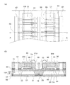
図1は、本発明の実施形態1に係るインクジェット式記録ヘッドを示す分解斜視図であり、図2は、図1の平面図及び断面図であり、図3は、流路形成基板の平面図及びそのB−B′断面図である。図示するように、流路形成基板10は、本実施形態では面方位(110)のシリコン単結晶基板からなり、その一方の面には予め熱酸化によって形成された厚さ0.5〜2μmの二酸化シリコンからなる弾性膜50が設けられている。この流路形成基板10には、隔壁11によって画成された複数の圧力発生室12が並設された列13が2列設けられている。また、流路形成基板10の圧力発生室12の各列13の外側の領域にはそれぞれ連通部14が形成され、連通部14と各圧力発生室12とがインク供給路15を介して連通されている。連通部14は、後述する保護基板30のリザーバ部32と連通して各圧力発生室12の共通のインク室となるリザーバ100の一部を構成する。インク供給路15は、圧力発生室12よりも狭い幅で形成されており、連通部14から圧力発生室12に流入するインクの流路抵抗を一定に保持している。なお、これらの圧力発生室12、連通部14及びインク供給路15は、面方位(110)のシリコン単結晶基板である流路形成基板10を異方性エッチングすることにより形成されている。
Hereinafter, the present invention will be described in detail based on embodiments.
(Embodiment 1)
1 is an exploded perspective view showing an ink jet recording head according to Embodiment 1 of the present invention, FIG. 2 is a plan view and a sectional view of FIG. 1, and FIG. 3 is a plan view of a flow path forming substrate. And FIG. As shown in the drawing, the flow
さらに、この流路形成基板10の少なくとも圧力発発生室12の列13の周囲には、図3(a)に示すように、溝部16が、圧力発生室12の列13の周囲にその三方を囲むように連続的に設けられている。例えば、本実施形態では、溝部16は、圧力発生室12の列13の間の領域から、圧力発生室12の並設方向両外側の領域まで連続的に設けられ、圧力発生室12の並設方向外側の領域では、インク供給路15及び連通部14に対応する領域まで連続的に形成されている。そして、この溝部16には、後述するノズルプレート20と流路形成基板10とを接着するための接着剤25が流れ込んだ状態となっている。
Further, at least around the
また、この溝部16は、少なくとも一部に流路形成基板10を貫通しない非貫通部を有し、例えば、本実施形態では、溝部16が非貫通部のみで構成されている。具体的には、図3(b)に示すように、溝部16は、複数の凹部17が連結されて連続的に形成され、且つ全ての領域において流路形成基板10を厚さ方向に貫通することなく形成されている。なお、溝部16は、流路形成基板10を異方性エッチングすることによって圧力発生室12等と同時に形成され、溝部16の内面には、圧力発生室12の内面と同一の結晶面で構成されている。
Moreover, this
ここで、異方性エッチングは、シリコン単結晶基板のエッチングレートの違いを利用して行われる。例えば、本実施形態では、面方位(110)のシリコン単結晶基板である流路形成基板10をKOH等のアルカリ溶液に浸漬すると、流路形成基板10が徐々に侵食されて表面の(110)面に垂直な第1の(111)面と、この第1の(111)面と約70度の角度をなし且つ表面の(110)面と約35度の角度をなす第2の(111)面とが出現する。そして、(110)面のエッチングレートと比較して(111)面のエッチングレートが約1/180であるため、この(111)面が出現することで実質的にエッチングが終了する。
Here, the anisotropic etching is performed by utilizing the difference in etching rate of the silicon single crystal substrate. For example, in this embodiment, when the flow
本実施形態では、各圧力発生室12の長辺を第1の(111)面で、短辺を第2の(111)面で形成している。また、この圧力発生室12は、流路形成基板10をほぼ貫通して弾性膜50に達するまでエッチングすることにより形成されている。なお、弾性膜50も、シリコン単結晶基板をエッチングするアルカリ溶液に侵される量がきわめて小さいため、弾性膜50に達するまで流路形成基板10をエッチングすることで、深さ方向のエッチングも実質的に終了する。
In the present embodiment, the long side of each
また、溝部16も圧力発生室と同様に流路形成基板10を異方性エッチングすることによって形成されており、溝部16の内面も上記第1の(111)及び第2の(111)面で構成されている。但し、溝部16は、上述したように、圧力発生室12等とは異なり流路形成基板10を厚さ方向に貫通することなく形成されるようにしている。なお、この点については、詳しく後述する。
Similarly to the pressure generation chamber, the
流路形成基板10の厚さは、圧力発生室12を配列密度に合わせて最適な厚さを選択すればよく、例えば、180dpi程度の配列密度であれば、流路形成基板10の厚さは、220μm程度であればよいが、本実施形態では、圧力発生室12を200dpi以上と比較的高密度に配列しているため、流路形成基板10の厚さは、100μm以下、本実施形態では、70μm程度と比較的薄くするのが好ましい。これは、隣接する圧力発生室12間の隔壁11の剛性を保ちつつ、配列密度を高くできるからである。
The thickness of the flow
流路形成基板10の開口面側には、圧力発生室12を形成する際のマスクとして用いられるマスク膜52を介して、各圧力発生室12のインク供給路15とは反対側の端部近傍に連通するノズル開口21が穿設されたノズルプレート20が接着剤25を介して固着されている。なお、ノズルプレート20は、厚さが例えば、0.01〜1mmで、線膨張係数が300℃以下で、例えば2.5〜4.5[×10-6/℃]であるガラスセラミックス、シリコン単結晶基板又はステンレス鋼などからなる。
On the opening surface side of the flow
一方、このような流路形成基板10の開口面とは反対側には、上述したように、厚さが例えば約1.0μmの弾性膜50が形成され、この弾性膜50上には、酸化ジルコニウム等からなり厚さが例えば、約0.4μmの絶縁体膜55が形成されている。さらに、この絶縁体膜55上には、白金及びイリジウム等からなり厚さが例えば、約0.2μmの下電極膜60と、チタン酸ジルコン酸鉛(PZT)等からなり厚さが例えば、約1.0μmの圧電体層70と、イリジウム等からなり厚さが例えば、約0.05μmの上電極膜80とが、後述するプロセスで積層形成されて、圧電素子300を構成している。ここで、圧電素子300は、下電極膜60、圧電体層70及び上電極膜80を含む部分をいう。一般的には、圧電素子300の何れか一方の電極を共通電極とし、他方の電極及び圧電体層70を各圧力発生室12毎にパターニングして構成する。そして、ここではパターニングされた何れか一方の電極及び圧電体層70から構成され、両電極への電圧の印加により圧電歪みが生じる部分を圧電体能動部という。本実施形態では、下電極膜60は圧電素子300の共通電極とし、上電極膜80を圧電素子300の個別電極としているが、駆動回路や配線の都合でこれを逆にしても支障はない。何れの場合においても、各圧力発生室毎に圧電体能動部が形成されていることになる。また、ここでは、圧電素子300と当該圧電素子300の駆動により変位が生じる振動板とを合わせて圧電アクチュエータと称する。上述した例では、弾性膜50、絶縁体膜55及び下電極膜60が振動板としての役割を果たす。
On the other hand, as described above, the
また、このような各圧電素子300の上電極膜80には、例えば、金(Au)等からなるリード電極90がそれぞれ接続され、このリード電極90を介して各圧電素子300に選択的に電圧が印加されるようになっている。
In addition, a
流路形成基板10の圧電素子300側の面には、圧電素子300に対向する領域に圧電素子保持部31を有する保護基板30が接着剤35によって接着されている。この圧電素子保持部31は、複数の圧電素子300を一体的に覆う大きさで形成されており、各圧電素子300は、この圧電素子保持部31内に配置されている。これにより、各圧電素子300は、外部環境の影響を殆ど受けない状態に保護されている。なお、この圧電素子保持部31は、必ずしも密封されている必要はない。
A
また、保護基板30には、リザーバ100の少なくとも一部を構成するリザーバ部32が設けられている。このリザーバ部32は、上述したように流路形成基板10の連通部13と連通され、これらリザーバ部32及び連通部14によってリザーバ100が形成されている。なお、保護基板30の材料としては、例えば、ガラス、セラミックス材料、金属、樹脂等が挙げられるが、流路形成基板10の熱膨張率と略同一の材料で形成されていることがより好ましく、本実施形態では、流路形成基板10と同一材料のシリコン単結晶基板を用いて形成した。
In addition, the
保護基板30上の圧力発生室12の各列に対応する領域のそれぞれには、並設された2列の圧電素子300をそれぞれ選択的に駆動するための2つの駆動IC200が実装されている。そして、駆動IC200と各圧電素子300から引き出されたリード電極90とが、保護基板30に設けられた貫通孔33を介して延設されるボンディングワイヤからなる駆動配線210によって電気的に接続されている。
Two
また、保護基板30上のリザーバ部32に対向する領域には、封止膜41及び固定板42とからなるコンプライアンス基板40が接合されている。ここで、封止膜41は、剛性が低く可撓性を有する材料(例えば、厚さが6μmのポリフェニレンサルファイド(PPS)フィルム)からなり、この封止膜41によってリザーバ部31の一方面が封止されている。また、固定板42は、金属等の硬質の材料(例えば、厚さが30μmのステンレス鋼(SUS)等)で形成される。この固定板42のリザーバ100に対向する領域は、厚さ方向に完全に除去された開口部43となっているため、リザーバ100の一方面は可撓性を有する封止膜41のみで封止され、内部圧力の変化によって変形可能な可撓部となっている。
In addition, a
このような本実施形態のインクジェット式記録ヘッドでは、図示しない外部インク供給手段と接続したインク導入口からインクを取り込み、リザーバ100からノズル開口21に至るまで内部をインクで満たした後、図示しない外部の駆動回路からの記録信号に従い、圧力発生室12に対応するそれぞれの下電極膜60と上電極膜80との間に電圧を印加し、弾性膜50、絶縁体膜55、下電極膜60及び圧電体層70をたわみ変形させることにより、各圧力発生室12内の圧力が高まりノズル開口21からインク滴が吐出する。
In such an ink jet recording head of this embodiment, after taking ink from an ink introduction port connected to an external ink supply means (not shown) and filling the interior from the
以下、このようなインクジェット式記録ヘッドの製造方法について、図4〜図8を参照して説明する。なお、図4〜図6は、圧力発生室12の長手方向の断面図である。また、図7及び図8は、マスク膜52の開口部53のパターン形状を示す図である。
Hereinafter, a method for manufacturing such an ink jet recording head will be described with reference to FIGS. 4 to 6 are sectional views of the
まず、図4(a)に示すように、シリコンウェハからなり流路形成基板10が複数一体的に形成される流路形成基板用ウェハ110を約1100℃の拡散炉で熱酸化し、その表面に弾性膜50を構成する二酸化シリコン膜51を形成する。なお、本実施形態では、流路形成基板用ウェハ110として、膜厚が約625μmと比較的厚く剛性の高いシリコンウェハを用いている。
First, as shown in FIG. 4A, a flow path forming
次に、図4(b)に示すように、弾性膜50(二酸化シリコン膜51)上に、酸化ジルコニウムからなる絶縁体膜55を形成する。具体的には、弾性膜50(二酸化シリコン膜51)上に、例えば、スパッタ法等によりジルコニウム(Zr)層を形成後、このジルコニウム層を、例えば、500〜1200℃の拡散炉で熱酸化することにより酸化ジルコニウム(ZrO2)からなる絶縁体膜55を形成する。
Next, as shown in FIG. 4B, an
次いで、図4(c)に示すように、例えば、白金とイリジウムとを絶縁体膜55上に積層することにより下電極膜60を形成した後、この下電極膜60を所定形状にパターニングする。次に、図4(d)に示すように、例えば、チタン酸ジルコン酸鉛(PZT)等からなる圧電体層70と、例えば、イリジウムからなる上電極膜80とを流路形成基板用ウェハ110の全面に形成し、これら圧電体層70及び上電極膜80を、各圧力発生室12に対向する領域にパターニングして圧電素子300を形成する。
Next, as shown in FIG. 4C, for example, after the
なお、圧電素子300を構成する圧電体層70の材料としては、例えば、チタン酸ジルコン酸鉛(PZT)等の強誘電性圧電性材料や、これにニオブ、ニッケル、マグネシウム、ビスマス又はイッテルビウム等の金属を添加したリラクサ強誘電体等が用いられる。その組成は、圧電素子300の特性、用途等を考慮して適宜選択すればよいが、例えば、PbTiO3(PT)、PbZrO3(PZ)、Pb(ZrxTi1−x)O3(PZT)、Pb(Mg1/3Nb2/3)O3−PbTiO3(PMN−PT)、Pb(Zn1/3Nb2/3)O3−PbTiO3(PZN−PT)、Pb(Ni1/3Nb2/3)O3−PbTiO3(PNN−PT)、Pb(In1/2Nb1/2)O3−PbTiO3(PIN−PT)、Pb(Sc1/3Ta1/2)O3−PbTiO3(PST−PT)、Pb(Sc1/3Nb1/2)O3−PbTiO3(PSN−PT)、BiScO3−PbTiO3(BS−PT)、BiYbO3−PbTiO3(BY−PT)等が挙げられる。
The material of the
また、圧電体層70の形成方法は、特に限定されないが、例えば、本実施形態では、金属有機物を触媒に溶解・分散したいわゆるゾルを塗布乾燥してゲル化し、さらに高温で焼成することで金属酸化物からなる圧電体層70を得る、いわゆるゾル−ゲル法を用いて圧電体層70を形成した。
The method for forming the
次に、図5(a)に示すように、リード電極90を形成する。具体的には、まず流路形成基板用ウェハ110の全面に亘って、例えば、金(Au)等からなる金属層を形成する。そして、この金属層上に、例えば、レジスト等からなるマスクパターン(図示なし)を形成し、このマスクパターンを介して金属層を圧電素子300毎にパターニングすることによりリード電極90を形成する。
Next, as shown in FIG. 5A, a
次に、図5(b)に示すように、保護基板30が複数一体的に形成される保護基板用ウェハ130を、流路形成基板用ウェハ110上に接着剤35によって接着する。ここで、保護基板用ウェハ130には、圧電素子保持部31、リザーバ部32等が予め形成されている。また、保護基板用ウェハ130は、例えば、400μm程度の厚さを有するシリコンウェハであり、保護基板用ウェハ130を接合することで流路形成基板用ウェハ110の剛性は著しく向上することになる。
Next, as shown in FIG. 5B, a
次いで、図5(c)に示すように、流路形成基板用ウェハ110をある程度の厚さとなるまで研磨した後、更に弗化硝酸によってウェットエッチングすることにより流路形成基板用ウェハ110を所定の厚みにする。例えば、本実施形態では、研磨及びウェットエッチングによって、流路形成基板用ウェハ110を、約70μmの厚さとなるように加工した。次いで、図6(a)に示すように、流路形成基板用ウェハ110上に、例えば、窒化シリコン(SiN)からなるマスク膜52を新たに形成し、所定形状にパターニングする。そして、図6(b)に示すように、このマスク膜52を介して流路形成基板用ウェハ110を異方性エッチング(ウェットエッチング)して、流路形成基板用ウェハ110に圧力発生室12、連通部13及びインク供給路14等を形成する。具体的には、流路形成基板用ウェハ110を、例えば、水酸化カリウム(KOH)水溶液等のエッチング液によって弾性膜50が露出するまでエッチングすることにより、圧力発生室12、連通部13及びインク供給路14を同時に形成する。
Next, as shown in FIG. 5C, after the flow path forming
また、本発明では、流路形成基板用ウェハ110を異方性エッチングすることにより圧力発生室12等を形成する際に、同時に溝部16を形成する。すなわち、マスク膜52に形成された複数の開口部を介して流路形成基板用ウェハ110を異方性エッチングすることにより、上述したように所定の領域に連続する溝部16が、流路形成基板用ウェハ110を厚さ方向に貫通することなく形成される。
Further, in the present invention, when the
ここで、溝部16を形成するために形成されるマスク膜52の開口部の形状は、適宜決定されればよいが、溝部16の位置によって異なる。具体的には、圧力発生室12の列13の間の領域の溝部16を形成するための各開口部53は、例えば、本実施形態では、図7(a)に示すようにそれぞれ略L字形状となるように形成した。そして、このような各開口部53Aは、隣接する開口部53Aと、溝部16の長さ方向で若干重なるように形成する。一方、圧力発生室12の並設方向外側の領域の溝部16を形成するための開口部53Bは、例えば、図8(a)に示すように略S字形状となるように形成した。そして、これら各開口部53Bも、開口部53Aと同様に、溝部16の長さ方向で隣接する開口部53Bと若干重なるように形成する。なお、ここで言う溝部16の長さ方向とは、圧力発生室12の列13の間の領域では、圧力発生室12の並設方向であり、圧力発生室12の並設方向外側の領域では、圧力発生室12の並設方向に直交する方向である。
Here, the shape of the opening of the
そして、このような複数の開口部53A,53Bから流路形成基板用ウェハ110を異方性エッチングすると、上述したように、流路形成基板用ウェハ110が徐々に侵食されて表面の(110)面に垂直な第1の(111)面と、この第1の(111)面と約70度の角度をなし且つ表面の(110)面と約35度の角度をなす第2の(111)面とが出現して凹部17が形成されていく。また同時に、図7(b)及び図8(b)に示すように、マスク膜52もエッチングされて開口部53A,53Bの領域が徐々に広がっていく(図7(c)及び図8(c))。そして、図7(d)及び図8(d)に示すように、最終的に開口部53A,53Bがそれぞれ繋がり、繋がった部分の流路形成基板用ウェハ110が除去されて各凹部17同士が連結される。これにより、所定の領域に溝部16が流路形成基板10を貫通することなく連続的に形成される(図3参照)。そして、このように形成された溝部16の内面は、圧力発生室12と同一の結晶面で構成される。
Then, when the flow path forming
なお、各溝部16(凹部17)の深さは、開口部53の幅及び長さによって決まり、溝部16の深さに応じて適宜決定する必要がある。ただし、マスク膜52の各開口部53をあまり広い範囲で重なるようにすると、各開口部53が早い段階で繋がってしまい流路形成基板用ウェハ110がエッチングされる量が多くなって溝部16の深さが深くなりすぎるため好ましくない。また、各開口部53の大きさがあまり小さすぎても、同様の理由によって溝部16が深くなりすぎてしまうため好ましくない。
In addition, the depth of each groove part 16 (concave part 17) is decided by the width and length of the opening part 53, and it is necessary to determine suitably according to the depth of the
このようにマスク膜52に設けられた所定形状の複数の開口部53を介して流路形成基板用ウェハ110を異方性エッチングして溝部16を形成することで、流路形成基板用ウェハ110を貫通することなく所定の深さの溝部16を比較的容易に形成することができる。また、流路形成基板用ウェハ110を貫通する圧力発生室12等の形成と同時に溝部16も形成することができるため、製造工程が煩雑化することもない。
Thus, the flow path forming
このように圧力発生室12、溝部16等を流路形成基板用ウェハ110に形成した後は、図6(c)に示すように、流路形成基板ウェハ110とノズルプレート20とを接着剤25を介して接着する。このとき、無駄な接着剤がこの溝部16に流れ込み、接着剤25が圧力発生室12あるいはノズル開口21等に過度に流れ込むことがない。本実施形態では、特に、圧力発生室12の列13の周囲の三方を囲むように、連続的に溝部16を設けるようにしたので、無駄な接着剤の量が比較的多い場合でも、圧力発生室12等への接着剤の流れ込みを確実に防止することができる。これにより、流路形成基板用ウェハ110(流路形成基板10)とノズルプレート20とを良好に接合することができ、接着による特性劣化を防止することができる。
After the
また、接着剤25が圧力発生室12内に流れ込んだ場合、接着剤25が振動板まで達すると、圧電素子300の駆動による振動板の変位量が低下するという問題が生じる。さらに、接着剤25の各圧力発生室12内への流れ込み量の違いによって、クロストークが発生するという問題も生じる。しかしながら本発明の構成によれば、このような問題の発生も確実に防止することができる。
Further, when the adhesive 25 flows into the
さらに、溝部16が流路形成基板用ウェハ110を貫通することなく形成されているため、流路形成基板用ウェハ110(流路形成基板10)の剛性が比較的高く維持される。例えば、溝部16が流路形成基板10の厚さの約半分程度の深さで形成されている場合、溝部が流路形成基板10を貫通している場合と比較して、約1.5倍程度、流路形成基板10の剛性が向上する。したがって、流路形成基板10(流路形成基板用ウェハ110)とノズルプレート20とを接着後に、これらが加熱された場合でも、熱膨張によって流路形成基板用ウェハ110(流路形成基板10)のクラックの発生を防止することができる。
Furthermore, since the
なお、このように流路形成基板用ウェハ110とノズルプレート20とを接着した後は、保護基板用ウェハ130にコンプライアンス基板40を接合し、流路形成基板用ウェハ110等の外周縁部の不要部分を、例えば、ダイシング等により切断することによって除去する。そして、これら流路形成基板用ウェハ110等を図1に示すような一つのチップサイズに分割することによって上述した構造のインクジェット式記録ヘッドが製造される。
After the flow path forming
(他の実施形態)
以上、本発明の各実施形態を説明したが、インクジェット式記録ヘッドの基本的構成は上述したものに限定されるものではない。また、このようなインクジェット式記録ヘッドは、インクカートリッジ等と連通するインク流路を具備する記録ヘッドユニットの一部を構成して、インクジェット式記録装置に搭載される。図9は、そのインクジェット式記録装置の一例を示す概略図である。図9に示すように、インクジェット式記録ヘッドを有する記録ヘッドユニット1A及び1Bは、インク供給手段を構成するカートリッジ2A及び2Bが着脱可能に設けられ、この記録ヘッドユニット1A及び1Bを搭載したキャリッジ3は、装置本体4に取り付けられたキャリッジ軸5に軸方向移動自在に設けられている。この記録ヘッドユニット1A及び1Bは、例えば、それぞれブラックインク組成物及びカラーインク組成物を吐出するものとしている。
(Other embodiments)
While the embodiments of the present invention have been described above, the basic configuration of the ink jet recording head is not limited to that described above. Such an ink jet recording head constitutes a part of a recording head unit including an ink flow path communicating with an ink cartridge or the like, and is mounted on the ink jet recording apparatus. FIG. 9 is a schematic view showing an example of the ink jet recording apparatus. As shown in FIG. 9, in the
そして、駆動モータ6の駆動力が図示しない複数の歯車およびタイミングベルト7を介してキャリッジ3に伝達されることで、記録ヘッドユニット1A及び1Bを搭載したキャリッジ3はキャリッジ軸5に沿って移動される。一方、装置本体4にはキャリッジ軸5に沿ってプラテン8が設けられており、図示しない給紙ローラなどにより給紙された紙等の記録媒体である記録シートSがプラテン8上を搬送されるようになっている。
The driving force of the driving
なお、上述した実施形態では、液体噴射ヘッドの一例としてインクジェット式記録ヘッドを挙げて説明したが、本発明は、広く液体噴射ヘッド全般を対象としたものであり、インク以外の液体を噴射する液体噴射ヘッドにも勿論適用することができる。その他の液体噴射ヘッドとしては、例えば、プリンタ等の画像記録装置に用いられる各種の記録ヘッド、液晶ディスプレー等のカラーフィルタの製造に用いられる色材噴射ヘッド、有機ELディスプレー、FED(面発光ディスプレー)等の電極形成に用いられる電極材料噴射ヘッド、バイオchip製造に用いられる生体有機物噴射ヘッド等が挙げられる。 In the above-described embodiment, an ink jet recording head has been described as an example of a liquid ejecting head. However, the present invention is intended for a wide range of liquid ejecting heads, and is a liquid that ejects liquids other than ink. Of course, the present invention can also be applied to an ejection head. Other liquid ejecting heads include, for example, various recording heads used in image recording apparatuses such as printers, color material ejecting heads used in manufacturing color filters such as liquid crystal displays, organic EL displays, and FEDs (surface emitting displays). Examples thereof include an electrode material ejection head used for electrode formation, a bioorganic matter ejection head used for biochip production, and the like.
10 流路形成基板、 12 圧力発生室、 14 連通部、 15 インク供給路、 16 溝部、 17 凹部、 20 ノズルプレート、 21 ノズル開口、 30 保護基板、 31 圧電素子保持部、 32 リザーバ部、 33 貫通孔、 40 コンプライアンス基板、 50 弾性膜、 52 マスク膜、 53 開口部、 55 絶縁体膜、 60 下電極膜、 70 圧電体層、 80 上電極膜、 90 リード電極、 100 リザーバ、 300 圧電素子
DESCRIPTION OF
Claims (1)
複数の前記開口部を、前記溝部の長さ方向で隣接する開口部と重なるよう配置して、隣接する前記凹部同士を当該凹部のエッチングの終点付近で繋げることで前記溝部とすることを特徴とする液体噴射ヘッドの製造方法。 A step of forming a piezoelectric element on one side of a flow path forming substrate made of a silicon single crystal substrate having a plane orientation (110), and wet etching the flow path forming substrate through a mask film having a predetermined shape. A plurality of pressure generating chambers that penetrate the flow path forming substrate in the thickness direction are formed, and at the same time, a groove portion having a non-penetrating portion that does not penetrate the flow path forming substrate is formed on the other surface side of the flow path forming substrate. Forming between the rows of generating chambers, and bonding the nozzle plate having a nozzle opening communicating with the pressure generating chamber on the other surface side of the flow path forming substrate with an adhesive, In the step of forming the groove, the flow path forming substrate is wet-etched from a plurality of independent openings provided in the mask film to form a plurality of recesses, and the adjacent recesses are formed at the top. The Shun groove portions to be linked,
A plurality of the openings are arranged so as to overlap with the openings adjacent in the length direction of the groove, and the adjacent recesses are connected in the vicinity of the end point of etching of the recess to form the groove. A method for manufacturing a liquid jet head.
Priority Applications (1)
| Application Number | Priority Date | Filing Date | Title |
|---|---|---|---|
| JP2004203735A JP4475042B2 (en) | 2004-07-09 | 2004-07-09 | Method for manufacturing liquid jet head |
Applications Claiming Priority (1)
| Application Number | Priority Date | Filing Date | Title |
|---|---|---|---|
| JP2004203735A JP4475042B2 (en) | 2004-07-09 | 2004-07-09 | Method for manufacturing liquid jet head |
Publications (3)
| Publication Number | Publication Date |
|---|---|
| JP2006021503A JP2006021503A (en) | 2006-01-26 |
| JP2006021503A5 JP2006021503A5 (en) | 2007-06-21 |
| JP4475042B2 true JP4475042B2 (en) | 2010-06-09 |
Family
ID=35795114
Family Applications (1)
| Application Number | Title | Priority Date | Filing Date |
|---|---|---|---|
| JP2004203735A Expired - Fee Related JP4475042B2 (en) | 2004-07-09 | 2004-07-09 | Method for manufacturing liquid jet head |
Country Status (1)
| Country | Link |
|---|---|
| JP (1) | JP4475042B2 (en) |
Families Citing this family (2)
| Publication number | Priority date | Publication date | Assignee | Title |
|---|---|---|---|---|
| JP5088690B2 (en) * | 2008-01-21 | 2012-12-05 | セイコーエプソン株式会社 | Liquid ejecting head and liquid ejecting apparatus |
| US8634005B2 (en) | 2008-09-30 | 2014-01-21 | Drs Rsta, Inc. | Very small pixel pitch focal plane array and method for manufacturing thereof |
-
2004
- 2004-07-09 JP JP2004203735A patent/JP4475042B2/en not_active Expired - Fee Related
Also Published As
| Publication number | Publication date |
|---|---|
| JP2006021503A (en) | 2006-01-26 |
Similar Documents
| Publication | Publication Date | Title |
|---|---|---|
| JP4258668B2 (en) | Liquid ejecting head and liquid ejecting apparatus | |
| JP5115330B2 (en) | Liquid ejecting head and liquid ejecting apparatus including the same | |
| JP2006231909A (en) | Liquid jetting head and liquid jetting apparatus | |
| JP2009160841A (en) | Method for manufacturing liquid jetting head, liquid jetting head and liquid jetting apparatus | |
| JP4614068B2 (en) | Liquid ejecting head, manufacturing method thereof, and liquid ejecting apparatus | |
| JP2009214522A (en) | Liquid jet head, method of manufacturing liquid jet head, and liquid jet device | |
| JP4553129B2 (en) | Liquid ejecting head and liquid ejecting apparatus | |
| JP2006255972A (en) | Liquid jetting head, and liquid jetting device | |
| JP4858670B2 (en) | Method for manufacturing actuator device and liquid ejecting apparatus | |
| JP4182360B2 (en) | Liquid ejecting head and liquid ejecting apparatus | |
| JP5257580B2 (en) | Liquid ejecting head, liquid ejecting apparatus, and piezoelectric element | |
| JP4442486B2 (en) | Method for manufacturing liquid jet head | |
| JP4591005B2 (en) | Method for manufacturing liquid jet head | |
| JP4623287B2 (en) | Liquid ejecting head, manufacturing method thereof, and liquid ejecting apparatus | |
| JP4475042B2 (en) | Method for manufacturing liquid jet head | |
| JP4645024B2 (en) | Method for manufacturing actuator device | |
| JP2007050673A (en) | Method for manufacturing liquid jetting head | |
| JP2006281603A (en) | Bonding method, manufacturing method of liquid jetting head, bonded substrate, liquid jetting head, and liquid jetting device | |
| JP5157127B2 (en) | Actuator device, manufacturing method thereof, liquid jet head, and liquid jet device | |
| JP5447786B2 (en) | Liquid ejecting head, liquid ejecting apparatus, and actuator device | |
| JP4911301B2 (en) | Micro device manufacturing method and liquid jet head manufacturing method | |
| JP2006224609A (en) | Method for manufacturing liquid injection head | |
| JP2009061729A (en) | Liquid injection head and liquid injection apparatus | |
| JP4433787B2 (en) | Liquid ejecting head, manufacturing method thereof, and liquid ejecting apparatus | |
| JP2010125682A (en) | Liquid jet head |
Legal Events
| Date | Code | Title | Description |
|---|---|---|---|
| A521 | Written amendment |
Free format text: JAPANESE INTERMEDIATE CODE: A523 Effective date: 20070426 |
|
| A621 | Written request for application examination |
Free format text: JAPANESE INTERMEDIATE CODE: A621 Effective date: 20070426 |
|
| A131 | Notification of reasons for refusal |
Free format text: JAPANESE INTERMEDIATE CODE: A131 Effective date: 20091202 |
|
| RD04 | Notification of resignation of power of attorney |
Free format text: JAPANESE INTERMEDIATE CODE: A7424 Effective date: 20091209 |
|
| A521 | Written amendment |
Free format text: JAPANESE INTERMEDIATE CODE: A523 Effective date: 20100127 |
|
| RD03 | Notification of appointment of power of attorney |
Free format text: JAPANESE INTERMEDIATE CODE: A7423 Effective date: 20100127 |
|
| TRDD | Decision of grant or rejection written | ||
| A01 | Written decision to grant a patent or to grant a registration (utility model) |
Free format text: JAPANESE INTERMEDIATE CODE: A01 Effective date: 20100216 |
|
| A01 | Written decision to grant a patent or to grant a registration (utility model) |
Free format text: JAPANESE INTERMEDIATE CODE: A01 |
|
| A61 | First payment of annual fees (during grant procedure) |
Free format text: JAPANESE INTERMEDIATE CODE: A61 Effective date: 20100301 |
|
| R150 | Certificate of patent or registration of utility model |
Ref document number: 4475042 Country of ref document: JP Free format text: JAPANESE INTERMEDIATE CODE: R150 Free format text: JAPANESE INTERMEDIATE CODE: R150 |
|
| FPAY | Renewal fee payment (event date is renewal date of database) |
Free format text: PAYMENT UNTIL: 20130319 Year of fee payment: 3 |
|
| FPAY | Renewal fee payment (event date is renewal date of database) |
Free format text: PAYMENT UNTIL: 20140319 Year of fee payment: 4 |
|
| S531 | Written request for registration of change of domicile |
Free format text: JAPANESE INTERMEDIATE CODE: R313531 |
|
| R350 | Written notification of registration of transfer |
Free format text: JAPANESE INTERMEDIATE CODE: R350 |
|
| LAPS | Cancellation because of no payment of annual fees |