EP1682447B1 - Formation of metal nanowires - Google Patents
Formation of metal nanowires Download PDFInfo
- Publication number
- EP1682447B1 EP1682447B1 EP04798395A EP04798395A EP1682447B1 EP 1682447 B1 EP1682447 B1 EP 1682447B1 EP 04798395 A EP04798395 A EP 04798395A EP 04798395 A EP04798395 A EP 04798395A EP 1682447 B1 EP1682447 B1 EP 1682447B1
- Authority
- EP
- European Patent Office
- Prior art keywords
- forming
- nanoparticles
- nanowire
- carbon
- molecules
- Prior art date
- Legal status (The legal status is an assumption and is not a legal conclusion. Google has not performed a legal analysis and makes no representation as to the accuracy of the status listed.)
- Expired - Lifetime
Links
- 239000002070 nanowire Substances 0.000 title claims abstract description 124
- 229910052751 metal Inorganic materials 0.000 title claims description 11
- 239000002184 metal Substances 0.000 title claims description 11
- 230000015572 biosynthetic process Effects 0.000 title description 27
- 238000000034 method Methods 0.000 claims abstract description 106
- 239000002105 nanoparticle Substances 0.000 claims abstract description 100
- OKTJSMMVPCPJKN-UHFFFAOYSA-N Carbon Chemical compound [C] OKTJSMMVPCPJKN-UHFFFAOYSA-N 0.000 claims abstract description 85
- 239000002071 nanotube Substances 0.000 claims abstract description 75
- 229910052799 carbon Inorganic materials 0.000 claims abstract description 54
- 239000000463 material Substances 0.000 claims abstract description 39
- 229920000642 polymer Polymers 0.000 claims abstract description 17
- 239000002245 particle Substances 0.000 claims abstract description 12
- 238000000151 deposition Methods 0.000 claims abstract description 10
- NBVXSUQYWXRMNV-UHFFFAOYSA-N fluoromethane Chemical compound FC NBVXSUQYWXRMNV-UHFFFAOYSA-N 0.000 claims abstract description 8
- 238000000354 decomposition reaction Methods 0.000 claims description 42
- PXHVJJICTQNCMI-UHFFFAOYSA-N Nickel Chemical compound [Ni] PXHVJJICTQNCMI-UHFFFAOYSA-N 0.000 claims description 27
- 229910002804 graphite Inorganic materials 0.000 claims description 25
- 239000010439 graphite Substances 0.000 claims description 25
- 230000008569 process Effects 0.000 claims description 25
- 229910017052 cobalt Inorganic materials 0.000 claims description 18
- 239000010941 cobalt Substances 0.000 claims description 18
- GUTLYIVDDKVIGB-UHFFFAOYSA-N cobalt atom Chemical compound [Co] GUTLYIVDDKVIGB-UHFFFAOYSA-N 0.000 claims description 17
- 238000000137 annealing Methods 0.000 claims description 15
- 229910052759 nickel Inorganic materials 0.000 claims description 13
- 239000012530 fluid Substances 0.000 claims description 9
- VNWKTOKETHGBQD-UHFFFAOYSA-N methane Chemical compound C VNWKTOKETHGBQD-UHFFFAOYSA-N 0.000 claims description 9
- XEEYBQQBJWHFJM-UHFFFAOYSA-N Iron Chemical compound [Fe] XEEYBQQBJWHFJM-UHFFFAOYSA-N 0.000 claims description 6
- 229910003481 amorphous carbon Inorganic materials 0.000 claims description 5
- KDLHZDBZIXYQEI-UHFFFAOYSA-N Palladium Chemical compound [Pd] KDLHZDBZIXYQEI-UHFFFAOYSA-N 0.000 claims description 4
- 230000002950 deficient Effects 0.000 claims description 4
- BASFCYQUMIYNBI-UHFFFAOYSA-N platinum Chemical compound [Pt] BASFCYQUMIYNBI-UHFFFAOYSA-N 0.000 claims description 4
- 229920000049 Carbon (fiber) Polymers 0.000 claims description 3
- 239000004917 carbon fiber Substances 0.000 claims description 3
- 239000003302 ferromagnetic material Substances 0.000 claims description 3
- 229910052742 iron Inorganic materials 0.000 claims description 3
- 150000002739 metals Chemical class 0.000 claims description 3
- 229910045601 alloy Inorganic materials 0.000 claims description 2
- 239000000956 alloy Substances 0.000 claims description 2
- 238000004581 coalescence Methods 0.000 claims description 2
- 229910052763 palladium Inorganic materials 0.000 claims description 2
- 229910052697 platinum Inorganic materials 0.000 claims description 2
- 239000007787 solid Substances 0.000 abstract description 8
- 239000007769 metal material Substances 0.000 abstract description 7
- 238000010438 heat treatment Methods 0.000 abstract description 4
- 238000004519 manufacturing process Methods 0.000 abstract description 4
- 238000005755 formation reaction Methods 0.000 description 27
- 239000000758 substrate Substances 0.000 description 17
- 239000007789 gas Substances 0.000 description 15
- 239000002041 carbon nanotube Substances 0.000 description 9
- 229910021393 carbon nanotube Inorganic materials 0.000 description 9
- 239000003153 chemical reaction reagent Substances 0.000 description 9
- 239000011148 porous material Substances 0.000 description 9
- RYGMFSIKBFXOCR-UHFFFAOYSA-N Copper Chemical compound [Cu] RYGMFSIKBFXOCR-UHFFFAOYSA-N 0.000 description 8
- 230000003197 catalytic effect Effects 0.000 description 8
- HSFWRNGVRCDJHI-UHFFFAOYSA-N alpha-acetylene Natural products C#C HSFWRNGVRCDJHI-UHFFFAOYSA-N 0.000 description 6
- 238000006243 chemical reaction Methods 0.000 description 5
- 229910052802 copper Inorganic materials 0.000 description 5
- 239000010949 copper Substances 0.000 description 5
- 125000002534 ethynyl group Chemical group [H]C#C* 0.000 description 5
- 230000005294 ferromagnetic effect Effects 0.000 description 5
- PCHJSUWPFVWCPO-UHFFFAOYSA-N gold Chemical compound [Au] PCHJSUWPFVWCPO-UHFFFAOYSA-N 0.000 description 5
- 229910052737 gold Inorganic materials 0.000 description 5
- 239000010931 gold Substances 0.000 description 5
- 239000002086 nanomaterial Substances 0.000 description 5
- 238000003917 TEM image Methods 0.000 description 4
- PNEYBMLMFCGWSK-UHFFFAOYSA-N aluminium oxide Inorganic materials [O-2].[O-2].[O-2].[Al+3].[Al+3] PNEYBMLMFCGWSK-UHFFFAOYSA-N 0.000 description 4
- 230000005684 electric field Effects 0.000 description 4
- 238000005334 plasma enhanced chemical vapour deposition Methods 0.000 description 4
- 238000000623 plasma-assisted chemical vapour deposition Methods 0.000 description 4
- 229910020323 ClF3 Inorganic materials 0.000 description 3
- 230000005540 biological transmission Effects 0.000 description 3
- 239000013078 crystal Substances 0.000 description 3
- 239000010408 film Substances 0.000 description 3
- 231100001261 hazardous Toxicity 0.000 description 3
- 239000002121 nanofiber Substances 0.000 description 3
- 239000000126 substance Substances 0.000 description 3
- QGZKDVFQNNGYKY-UHFFFAOYSA-N Ammonia Chemical compound N QGZKDVFQNNGYKY-UHFFFAOYSA-N 0.000 description 2
- IJGRMHOSHXDMSA-UHFFFAOYSA-N Atomic nitrogen Chemical compound N#N IJGRMHOSHXDMSA-UHFFFAOYSA-N 0.000 description 2
- XMWRBQBLMFGWIX-UHFFFAOYSA-N C60 fullerene Chemical compound C12=C3C(C4=C56)=C7C8=C5C5=C9C%10=C6C6=C4C1=C1C4=C6C6=C%10C%10=C9C9=C%11C5=C8C5=C8C7=C3C3=C7C2=C1C1=C2C4=C6C4=C%10C6=C9C9=C%11C5=C5C8=C3C3=C7C1=C1C2=C4C6=C2C9=C5C3=C12 XMWRBQBLMFGWIX-UHFFFAOYSA-N 0.000 description 2
- ZAMOUSCENKQFHK-UHFFFAOYSA-N Chlorine atom Chemical compound [Cl] ZAMOUSCENKQFHK-UHFFFAOYSA-N 0.000 description 2
- PXGOKWXKJXAPGV-UHFFFAOYSA-N Fluorine Chemical compound FF PXGOKWXKJXAPGV-UHFFFAOYSA-N 0.000 description 2
- 229920004459 Kel-F® PCTFE Polymers 0.000 description 2
- 238000005054 agglomeration Methods 0.000 description 2
- 230000002776 aggregation Effects 0.000 description 2
- 229910052801 chlorine Inorganic materials 0.000 description 2
- 239000000460 chlorine Substances 0.000 description 2
- UUAGAQFQZIEFAH-UHFFFAOYSA-N chlorotrifluoroethylene Chemical compound FC(F)=C(F)Cl UUAGAQFQZIEFAH-UHFFFAOYSA-N 0.000 description 2
- 230000008021 deposition Effects 0.000 description 2
- 238000005516 engineering process Methods 0.000 description 2
- 229910052731 fluorine Inorganic materials 0.000 description 2
- 239000011737 fluorine Substances 0.000 description 2
- 239000007788 liquid Substances 0.000 description 2
- 230000005291 magnetic effect Effects 0.000 description 2
- 239000000203 mixture Substances 0.000 description 2
- 239000000178 monomer Substances 0.000 description 2
- 239000002088 nanocapsule Substances 0.000 description 2
- -1 poly(chloro-trifluoro-ethene) Polymers 0.000 description 2
- 239000000843 powder Substances 0.000 description 2
- BBEAQIROQSPTKN-UHFFFAOYSA-N pyrene Chemical compound C1=CC=C2C=CC3=CC=CC4=CC=C1C2=C43 BBEAQIROQSPTKN-UHFFFAOYSA-N 0.000 description 2
- 238000003786 synthesis reaction Methods 0.000 description 2
- 230000002194 synthesizing effect Effects 0.000 description 2
- 239000010409 thin film Substances 0.000 description 2
- ZOXJGFHDIHLPTG-UHFFFAOYSA-N Boron Chemical compound [B] ZOXJGFHDIHLPTG-UHFFFAOYSA-N 0.000 description 1
- 229910001339 C alloy Inorganic materials 0.000 description 1
- 239000004215 Carbon black (E152) Substances 0.000 description 1
- CURLTUGMZLYLDI-UHFFFAOYSA-N Carbon dioxide Chemical compound O=C=O CURLTUGMZLYLDI-UHFFFAOYSA-N 0.000 description 1
- KZBUYRJDOAKODT-UHFFFAOYSA-N Chlorine Chemical compound ClCl KZBUYRJDOAKODT-UHFFFAOYSA-N 0.000 description 1
- UFHFLCQGNIYNRP-UHFFFAOYSA-N Hydrogen Chemical compound [H][H] UFHFLCQGNIYNRP-UHFFFAOYSA-N 0.000 description 1
- 241001424392 Lucia limbaria Species 0.000 description 1
- 230000004913 activation Effects 0.000 description 1
- 239000000853 adhesive Substances 0.000 description 1
- 230000001070 adhesive effect Effects 0.000 description 1
- 239000004411 aluminium Substances 0.000 description 1
- 229910052782 aluminium Inorganic materials 0.000 description 1
- XAGFODPZIPBFFR-UHFFFAOYSA-N aluminium Chemical compound [Al] XAGFODPZIPBFFR-UHFFFAOYSA-N 0.000 description 1
- 229910021529 ammonia Inorganic materials 0.000 description 1
- 229910052796 boron Inorganic materials 0.000 description 1
- 150000001721 carbon Chemical class 0.000 description 1
- 229910002090 carbon oxide Inorganic materials 0.000 description 1
- 150000001879 copper Chemical class 0.000 description 1
- 230000007547 defect Effects 0.000 description 1
- 230000001419 dependent effect Effects 0.000 description 1
- 229910001873 dinitrogen Inorganic materials 0.000 description 1
- 238000010891 electric arc Methods 0.000 description 1
- 238000002848 electrochemical method Methods 0.000 description 1
- 239000003792 electrolyte Substances 0.000 description 1
- 230000005669 field effect Effects 0.000 description 1
- GVEPBJHOBDJJJI-UHFFFAOYSA-N fluoranthrene Natural products C1=CC(C2=CC=CC=C22)=C3C2=CC=CC3=C1 GVEPBJHOBDJJJI-UHFFFAOYSA-N 0.000 description 1
- 239000011888 foil Substances 0.000 description 1
- 229910003472 fullerene Inorganic materials 0.000 description 1
- 239000001307 helium Substances 0.000 description 1
- 229910052734 helium Inorganic materials 0.000 description 1
- SWQJXJOGLNCZEY-UHFFFAOYSA-N helium atom Chemical compound [He] SWQJXJOGLNCZEY-UHFFFAOYSA-N 0.000 description 1
- 229930195733 hydrocarbon Natural products 0.000 description 1
- 150000002430 hydrocarbons Chemical class 0.000 description 1
- 239000001257 hydrogen Substances 0.000 description 1
- 229910052739 hydrogen Inorganic materials 0.000 description 1
- 230000003993 interaction Effects 0.000 description 1
- 150000002500 ions Chemical class 0.000 description 1
- 238000001459 lithography Methods 0.000 description 1
- 230000008018 melting Effects 0.000 description 1
- 238000002844 melting Methods 0.000 description 1
- 239000012528 membrane Substances 0.000 description 1
- 238000004377 microelectronic Methods 0.000 description 1
- 230000004048 modification Effects 0.000 description 1
- 238000012986 modification Methods 0.000 description 1
- JMANVNJQNLATNU-UHFFFAOYSA-N oxalonitrile Chemical compound N#CC#N JMANVNJQNLATNU-UHFFFAOYSA-N 0.000 description 1
- 125000005575 polycyclic aromatic hydrocarbon group Chemical group 0.000 description 1
- 239000002243 precursor Substances 0.000 description 1
- 239000010453 quartz Substances 0.000 description 1
- 238000001338 self-assembly Methods 0.000 description 1
- 239000004065 semiconductor Substances 0.000 description 1
- VYPSYNLAJGMNEJ-UHFFFAOYSA-N silicon dioxide Inorganic materials O=[Si]=O VYPSYNLAJGMNEJ-UHFFFAOYSA-N 0.000 description 1
- 238000005245 sintering Methods 0.000 description 1
- 230000002269 spontaneous effect Effects 0.000 description 1
- 229910001220 stainless steel Inorganic materials 0.000 description 1
- 239000010935 stainless steel Substances 0.000 description 1
- 230000007847 structural defect Effects 0.000 description 1
Images

Classifications
-
- C—CHEMISTRY; METALLURGY
- C04—CEMENTS; CONCRETE; ARTIFICIAL STONE; CERAMICS; REFRACTORIES
- C04B—LIME, MAGNESIA; SLAG; CEMENTS; COMPOSITIONS THEREOF, e.g. MORTARS, CONCRETE OR LIKE BUILDING MATERIALS; ARTIFICIAL STONE; CERAMICS; REFRACTORIES; TREATMENT OF NATURAL STONE
- C04B35/00—Shaped ceramic products characterised by their composition; Ceramics compositions; Processing powders of inorganic compounds preparatory to the manufacturing of ceramic products
- C04B35/622—Forming processes; Processing powders of inorganic compounds preparatory to the manufacturing of ceramic products
- C04B35/62227—Forming processes; Processing powders of inorganic compounds preparatory to the manufacturing of ceramic products obtaining fibres
- C04B35/62272—Forming processes; Processing powders of inorganic compounds preparatory to the manufacturing of ceramic products obtaining fibres based on non-oxide ceramics
- C04B35/62277—Fibres based on carbides
-
- B—PERFORMING OPERATIONS; TRANSPORTING
- B82—NANOTECHNOLOGY
- B82Y—SPECIFIC USES OR APPLICATIONS OF NANOSTRUCTURES; MEASUREMENT OR ANALYSIS OF NANOSTRUCTURES; MANUFACTURE OR TREATMENT OF NANOSTRUCTURES
- B82Y30/00—Nanotechnology for materials or surface science, e.g. nanocomposites
-
- C—CHEMISTRY; METALLURGY
- C01—INORGANIC CHEMISTRY
- C01B—NON-METALLIC ELEMENTS; COMPOUNDS THEREOF; METALLOIDS OR COMPOUNDS THEREOF NOT COVERED BY SUBCLASS C01C
- C01B32/00—Carbon; Compounds thereof
- C01B32/90—Carbides
- C01B32/914—Carbides of single elements
-
- C—CHEMISTRY; METALLURGY
- C04—CEMENTS; CONCRETE; ARTIFICIAL STONE; CERAMICS; REFRACTORIES
- C04B—LIME, MAGNESIA; SLAG; CEMENTS; COMPOSITIONS THEREOF, e.g. MORTARS, CONCRETE OR LIKE BUILDING MATERIALS; ARTIFICIAL STONE; CERAMICS; REFRACTORIES; TREATMENT OF NATURAL STONE
- C04B35/00—Shaped ceramic products characterised by their composition; Ceramics compositions; Processing powders of inorganic compounds preparatory to the manufacturing of ceramic products
- C04B35/622—Forming processes; Processing powders of inorganic compounds preparatory to the manufacturing of ceramic products
- C04B35/62227—Forming processes; Processing powders of inorganic compounds preparatory to the manufacturing of ceramic products obtaining fibres
-
- C—CHEMISTRY; METALLURGY
- C04—CEMENTS; CONCRETE; ARTIFICIAL STONE; CERAMICS; REFRACTORIES
- C04B—LIME, MAGNESIA; SLAG; CEMENTS; COMPOSITIONS THEREOF, e.g. MORTARS, CONCRETE OR LIKE BUILDING MATERIALS; ARTIFICIAL STONE; CERAMICS; REFRACTORIES; TREATMENT OF NATURAL STONE
- C04B2235/00—Aspects relating to ceramic starting mixtures or sintered ceramic products
- C04B2235/02—Composition of constituents of the starting material or of secondary phases of the final product
- C04B2235/30—Constituents and secondary phases not being of a fibrous nature
- C04B2235/40—Metallic constituents or additives not added as binding phase
- C04B2235/405—Iron group metals
-
- C—CHEMISTRY; METALLURGY
- C04—CEMENTS; CONCRETE; ARTIFICIAL STONE; CERAMICS; REFRACTORIES
- C04B—LIME, MAGNESIA; SLAG; CEMENTS; COMPOSITIONS THEREOF, e.g. MORTARS, CONCRETE OR LIKE BUILDING MATERIALS; ARTIFICIAL STONE; CERAMICS; REFRACTORIES; TREATMENT OF NATURAL STONE
- C04B2235/00—Aspects relating to ceramic starting mixtures or sintered ceramic products
- C04B2235/02—Composition of constituents of the starting material or of secondary phases of the final product
- C04B2235/50—Constituents or additives of the starting mixture chosen for their shape or used because of their shape or their physical appearance
- C04B2235/52—Constituents or additives characterised by their shapes
- C04B2235/5208—Fibers
- C04B2235/5264—Fibers characterised by the diameter of the fibers
-
- C—CHEMISTRY; METALLURGY
- C04—CEMENTS; CONCRETE; ARTIFICIAL STONE; CERAMICS; REFRACTORIES
- C04B—LIME, MAGNESIA; SLAG; CEMENTS; COMPOSITIONS THEREOF, e.g. MORTARS, CONCRETE OR LIKE BUILDING MATERIALS; ARTIFICIAL STONE; CERAMICS; REFRACTORIES; TREATMENT OF NATURAL STONE
- C04B2235/00—Aspects relating to ceramic starting mixtures or sintered ceramic products
- C04B2235/02—Composition of constituents of the starting material or of secondary phases of the final product
- C04B2235/50—Constituents or additives of the starting mixture chosen for their shape or used because of their shape or their physical appearance
- C04B2235/52—Constituents or additives characterised by their shapes
- C04B2235/5284—Hollow fibers, e.g. nanotubes
Definitions
- the present invention relates to methods of forming nanostructures, particularly to methods of forming nanowires and nanotubes.
- Nanotechnology is defined by the Institute of Nanotechnology in the UK as “science and technology where dimensions and tolerances in the range of 0.1 nanometers (nm) to 100nm play a critical role”.
- Nano-scale a nanoscale cross section
- nanostructures - structures which have at least one dimension at least approximately on the scale of 0.1 to 100nm (referred to as the "nano-scale”).
- nanostructures Two examples are nanowires and nanotubes, which each have a nano-scale cross section.
- Methods of forming nanostructures include methods based on the miniaturisation of technology developed initially at a scale greater than the nano-scale, and new methods for the formation of nanostructures from molecular elements.
- Nanowires are usually electrochemically based and involve the use of porous materials such as alumina.
- the pores of such materials are, for example, channels having the desired dimensions for the nanowires to be formed.
- Ions of the metal from which the nanowires are to be formed are contained in an electrolyte and are drawn into the channels by applying a voltage across two electrodes being positioned at either end of the channels.
- extracting the nanowires from the porous material commonly involves removal of the porous material.
- the nanowires formed in this process are often collected as a powder and the collection and manipulation of individual nanowires is a relatively time consuming, skillful and cost inefficient process. To date there is no automated process for the reliable manipulation of individual nanowires. This makes the use in industry of the nanowires produced by this process impractical. Additionally, the pores of the porous material are often machined to meet desired dimensions of the nanowires to be formed. This proves to be difficult if the dimensions of the pores are required to meet strict tolerances.
- Carbon nanotubes are commonly formed on a substrate having a ferromagnetic catalytic layer of for example, nickel.
- a carbon vapour plasma is formed by the decomposition of a gas, for example acetylene, due to heating and/or an application of an electric field.
- the carbon of the plasma reacts with the catalytic layer to form nanotubes which form vertically from the substrate and are approximately aligned with each other.
- the catalytic layer forms individual particles upon heating, each individual particle leading to the formation of one nanotube. Aligned nanotubes only usually form in the presence of an externally applied electric field.
- Ammonia and acetylene gases are introduced at this temperature and, using a plasma-enhanced chemical-vapour deposition (PECVD) technique, nanotubes are grown from the nickel nanoparticles, vertically to the substrate. An electric field induced by the plasma causes the nanotubes to be aligned.
- PECVD plasma-enhanced chemical-vapour deposition
- a well-formed nanotube may be considered to comprise a hollow tube having walls formed of curved sheets formed of, e.g. graphite. Each end of the hollow tube is capped with a fullerene hemisphere, typically formed of carbon.
- a nanofibre may be considered as a nanotube in which the sheet and fullerene structures comprise defects.
- the nanofibres are formed from nickel particles on a substrate using methane gas as the source of carbon.
- a radio-frequency voltage applied across the volume of methane creates a hydrocarbon plasma which provides the carbon required for nanofibre formation at the surface of the nickel particles.
- a nickel particle remains at a tip of each growing nanofibre and, although this method may be performed at room temperature, the radio-frequency PECVD causes superheating of this tip to a temperature of approximately 450-1250°C to provide a required energy for the reaction.
- the nanofibres formed by this method are not aligned but have what is referred to as a 'spaghetti morphology'.
- a method of forming a nanowire comprising:
- each of the molecules is a decomposition product. More preferably, the decomposition products form a vapour.
- the vapour is provided from a polymer which is initially solid and heated to reach a temperature of between 100 and 600°C; this causes decomposition of the polymer to form a vapour.
- a method of forming a nanotube comprising:
- the temperature of the method for forming the nanowires or the nanotubes is relatively low and allows reagents, which are unstable above these temperatures, to be used in the formation reaction. Additionally, the use of a vapour at such a relatively low temperature is less hazardous than using a flammable gas at relatively high temperatures.
- Nanowires and nanotubes formed at these relatively low temperatures can be formed to be substantially linear without the need for an externally applied magnetic or electric field. Furthermore the method of the present invention does not require the use of any plasma based technique. This provides a relatively simple and efficient method of forming nanowires and nanotubes.
- Apparatus for providing the method for forming the nanowires or nanotubes does not include a gas input system and is consequently relatively simple and cost efficient to install.
- nanowires of the present invention dimensions of the nanowires are not determined by a template material, for example a porous material such as alumina. Nanowires having consistent dimensions are efficiently formed without the need for the production of a template material having precise specifications.
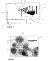
- FIG 1 shows schematically an apparatus for producing nanoparticles in accordance with an embodiment of the present invention.
- the particles are of a metallic material and are provided for the method of forming a nanowire or a nanotube in accordance with embodiments of the present invention.
- the particles are nanoparticles, each of which has at least one dimension on the nano-scale.
- the metallic material in this embodiment is cobalt carbide (Co 3 C) which is an alloy of a ferromagnetic material which in this case is the metal cobalt (Co).
- the cobalt carbide is formed using a carbon arc technique.
- the carbon arc technique involves a cathode 2 formed of graphite, and an anode 4 formed of a mixture of compressed graphite and cobalt powders. The mixture comprises approximately 30-50% by weight of cobalt.
- a voltaic arc is initiated between the cathode 2 and the anode 4 using a DC electric power source 5, which produces an arc spot 6 on the cathode 2.
- a plasma 8 is formed between the anode 4 and a substrate 10. The plasma 8 occupies an area which expands in a direction from the cathode 2 and the anode 4 towards the substrate 10. Nitrogen (N 2 ) gas flows through an opening 7 within the anode 4 into a region of the plasma 8.
- the substrate in this example is formed of a foil of aluminium (Al).
- Cobalt carbide nanoparticles 12 are formed by this carbon arc technique and are carried by the expanding plasma 8 and deposited on the substrate 10.
- the carbon arc technique is performed in a reduced pressure environment, preferably a substantial vacuum.
- a substantial vacuum we mean a reduced pressure which is at least an order of magnitude lower than atmospheric pressure. This substantial vacuum is provided by removal 14 of atmospheric molecules in a reaction chamber 13 using a vacuum pump.
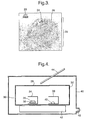
- FIG. 2 shows an image of the cobalt carbide nanoparticles 12 formed using the described carbon arc technique. Note that the images shown herein are recorded using a high resolution electron microscope (HREM). As can be seen, the nanoparticles 12 are approximately spherical and have a core region 16 and a perimeter region 18. The scale bar 20 indicates the average diameter of the nanoparticles 12 in this example to be approximately 5 nm. The core region 16 comprises cobalt carbide and therefore a relatively high proportion of carbon.
- HREM high resolution electron microscope
- Figure 3 shows an image of a nanoparticle 12 following an annealing process.
- an annealing process the relatively high proportion of carbon of the core region 16 moves to the perimeter region 18.
- the annealing process involves heating the nanoparticles 12 in a substantial vacuum to a temperature of between 300 and 600°C, in this embodiment approximately 375°C for a selected period of between 5 and 100 hours, in this embodiment approximately 72 hours.
- the nanoparticles 12 following the annealing process are annealed nanoparticles 22 and have a core region 24 and a perimeter region 26.
- the core region 24 of the annealed nanoparticles comprises substantially only cobalt and therefore a relatively low proportion of carbon.
- the annealed perimeter region 26 comprises a high proportion of carbon which is arranged in layers of graphite. Following removal of the carbon from the core region 16, the annealed core region 24 has an increased magnetisation of a multiple of approximately 100.
- the scale bar 28 indicates the average diameter of this annealed nanoparticle 22 to be approximately 10 to 12nm.
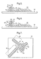
- FIG. 4 shows schematically an apparatus for a method of forming a nanowire or a nanotube in accordance with embodiments of the present invention.
- a reaction vessel is a tube 28 formed of a metal, which in this case is stainless steel, and has a length of approximately 20cm and a width of approximately 6cm.
- a first end 30 of the tube 28 is sealed and a second end 32 of the tube 28 is perforated.
- Inside the tube 28 is a first reagent vessel 34 and a second reagent vessel 36, both reagent vessels being beakers with a volume of approximately 5 ml and being formed of quartz.
- the first and the second reagent vessels 34, 36 lie on one side and an open end of each vessel faces the sealed first end 32.
- the first reagent vessel 34 contains a plurality of agglomerated masses of nanoparticles 35 arranged on a substrate.
- the nanoparticles 35 are the nanoparticles 22 formed using the carbon arc technique described earlier, without having being annealed.
- the substrate in this example is a grid 38, formed of copper, for use in a transmission electron microscope (TEM).
- TEM transmission electron microscope
- the agglomerated masses of nanoparticles 35 rest on a film of carbon comprising layers of amorphous carbon which is supported on a surface of the TEM grid 38.
- the carbon comprising layers may include a carbon nitride or carbon oxide support layer.
- the second reagent vessel 36 contains a plurality of molecules 40 which are in the form of an initially solid polymer.
- Nanowire or nanotube formation conditions are provided by the apparatus and include applying heat to reach a temperature T which is arranged to both melt the solid polymer 40 and to prevent a coalescence of the nanoparticles 36.
- the temperature T is below 600°C, and preferably above 100°C. More preferably, the temperature T is below 500°C and above 150°C. In this embodiment, the temperature used was approximately 375°C.
- a heater 42 provides the heat to reach this temperature T and a thermocouple 44 aids regulation of the temperature T.
- the nanowire or nanotube formation conditions further include providing a substantial vacuum, in this embodiment approximately 10 -6 mbar prior to providing the temperature T.
- the tube 28 is placed inside a vacuum chamber 46, from which atmospheric gas is removed 48 with a pump, to provide the substantial vacuum.
- the nanowire or nanotube formation conditions are provided for a period of between 3 and 100 hours, in this embodiment approximately 72 hours.
- the initially solid polymer once melted, decomposes to form a vapour of decomposition products.
- decomposition products include molecules which contain carbon and which form a fluid of molecules.
- Figure 5 shows schematically a step of forming a nanowire in accordance with an embodiment of the present invention.
- a method of forming a nanowire comprises providing an agglomeration of cobalt carbide nanoparticles 50 on a carbon film of the TEM copper grid 52, in accordance with the already described nanowire formation apparatus.
- the molecules of the vapour contain carbon and are in this embodiment fluorocarbon decomposition products R 1 , typically having a chemical formula C 2 ClF 3 .
- the initially solid polymer which provides these fluorocarbon decomposition products R 1 is poly(chloro-trifluoro-ethene) which has a chemical formula (C 2 ClF 3 ) n , where n is the number of monomer units in the polymer molecules.
- This polymer has the trade name Kel-F ® and has a melting point of approximately 200°C.
- the decomposition products R 1 Upon providing the nanowire formation conditions, the decomposition products R 1 reach the agglomerate of nanoparticles 50 including one nanoparticle 54.
- the decomposition products R 1 are believed to interact with an exterior 55 of the nanoparticles 50 as indicated by arrows in figure 5, and further decomposition of the decomposition products R 1 is caused by catalytic action of the nanoparticles 50.
- the further decomposition of the decomposition products R 1 yields carbon, fluorine (F 2 ) and chlorine (Cl 2 ).
- At least some of the carbon of the decomposition products R 1 is deposited onto the exterior of the one nanoparticle 54 to form a layer of carbon which surrounds at least part of the exterior 55.
- the layer of carbon comprises graphite and comprises a plurality of layers of graphite 56.
- Figure 6 shows schematically a further step of forming a nanowire.
- further decomposition of the decomposition products R 1 is provided by the catalytic action of nanoparticles 50 within the vicinity of the one nanoparticle 54.
- At least some of the carbon of the decomposition products R 1 is deposited onto the layer of carbon which surrounds at least part of the exterior 55 of the one nanoparticle 54 to form a nanotube enclosing an elongate space.
- the one nanoparticle 54 assembles with further of the nanoparticles 50 including the further nanoparticle 58 to form an elongate configuration of nanoparticles which is a nanowire 60, within the nanotube.
- the nanotube comprises layers of graphite.
- the nanotube may include defective graphite, amorphous carbon and/or carbon fiber.
- Figure 7 shows schematically as a top view, a formation of a plurality of the nanowires according to the method of forming nanowires of this embodiment of the present invention. Note that a plurality of nanowires 60 is formed from a single agglomerated mass of nanoparticles 50. The nanowires 60, once formed, are typically substantially linear.
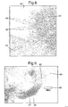
- Figure 8 shows a top view of the formation of the plurality of nanowires 60.
- the image taken using a transmission electron microscope (TEM), has a scale bar 62 which indicates the average diameter of each nanowire 60 to be approximately 15 to 25nm. Within this image, the agglomerated mass 64, from which the plurality of nanowires 60 is formed is readily distinguished.
- the image of Figure 8 is taken looking down towards the surface of the TEM grid 52 on which the nanoparticles 50 are mounted. Nanowires 60 are seen forming in directions approximately parallel a plane of the surface of the TEM grid 52. It is noted that nanowires 60 may also form in further directions, including a direction perpendicular to the plane mentioned above.
- Figure 9 shows a further TEM image of the nanowires 60 at a higher magnification.
- the scale bar 66 indicates the average width of the nanowires 60 to be approximately 5 nm. The closer magnification of this image allows detail of the nanowires 60 to be seen.
- the nanowires 60 have a core region 67 which corresponds to the nanoparticles 50, including the one nanoparticle 54 and the further nanoparticles 58, within the graphite layer 68 of the nanowire 60. From Figure 9 it can be seen that the core region 67 of cobalt carbide generally has an approximately regular crystalline structure.
- Figure 10 shows a TEM image of a further nanowire formed in accordance with this embodiment.
- the nanowire is similar to those described above and illustrated in Figure 9.
- the scale bar 69 indicates the average diameter of the nanowires to be approximately 11nm.
- a core region 70 of this nanowire and a graphite layer 71 are similar to the core region 67 and the graphite layer 68 of the nanowire 60 described using Figure 9 except that the core region 70 has a considerably less regular crystalline structure and the graphite layer 71 comprises structural defects.
- Figure 11 shows a TEM image of a nanowire following an annealing process.
- the annealing process for the nanowires 60 used involves applying heat to reach a temperature of between 300 and 600°C, in this embodiment approximately 375°C.
- the nanowires 60 are annealed at this temperature for an appropriate amount of time.
- the annealing process causes at least a majority of carbon in the core region 67 of the nanowires 60 to move to the graphite layer 68. Additionally the annealing process helps to pack atoms of the core region 67 more closely by a sintering process.
- Nitrogen gas may be used to provide a non-reactive environment during this annealing process.
- the annealed nanowires comprise an annealed core region 73 which has a substantially continuous crystalline structure which is substantially consistent with a crystal structure projection of delta-cobalt ( ⁇ -Co). This crystalline structure is similar to that of the annealed core region 24 of the annealed nanoparticles.
- an annealed graphite layer 74 Surrounding this is an annealed graphite layer 74 which comprises a greater plurality of graphite layers than the graphite layer of the nanowire 60 prior to the annealing process.
- the scale bar 72 indicates the average diameter of the annealed nanowires to be approximately 8nm.
- Figure 12 shows a TEM image of nanowires formed in accordance with a different embodiment of the present invention.
- the nanoparticles provided on the TEM grid are cobalt carbide nanoparticles formed in the carbon arc technique, having subsequently been annealed, as described earlier and illustrated in Figure 3.
- Nanowires are formed using the annealed nanoparticles according to the method described above for the previous embodiment.
- Figure 11 shows nanowires 76 formed according to the method of this embodiment.
- the scale bar 78 indicates the average diameter of the nanowires to be approximately 15 to 25nm. Additionally, the length of the nanowires 76 is often in excess of 500nm.
- the assembling step of the nanoparticles according to this embodiment proceeds at a higher rate than for the non-annealed nanoparticles of previously described embodiments. This is indicated by the relatively long length of at least some of the nanowires (above 500nm).
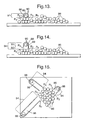
- Figure 13 shows schematically a step of forming a nanotube according to an embodiment of the present invention. In this embodiment, a similar process to that described above is provided, except that a substantially hollow nanotube is formed.
- an agglomeration of cobalt carbide nanoparticles 86 are provided on a TEM copper grid.
- the nanoparticles 86 of this embodiment are the nanoparticles formed in the carbon arc technique described earlier which have not been subsequently annealed.
- the density of the nanoparticles in the agglomerate in this embodiment is, however, less than a density of the nanoparticles in the agglomerate used in the above embodiments to form nanowires.
- the nanoparticles are then exposed to a vapour under nanotube formation conditions.
- the molecules of the vapour are fluorocarbon molecules which contain carbon and are fluorocarbon decomposition products R 2 , typically having a chemical formula C 2 ClF 3 .
- the initially solid polymer which provides these decomposition products R 2 is in this embodiment Kel-F ® , as described in further detail above.
- the decomposition products R 2 Upon providing the nanotube formation conditions, the decomposition products R 2 reach the nanoparticles 86 including the nanoparticle 88 shown. The decomposition products R 2 are believed to interact with an exterior 89 of the nanoparticles 86 as indicated by arrows in Figure 13, and further decomposition of the decomposition products R 2 is caused by catalytic action of the nanoparticles 86. The further decomposition of the decomposition products R 2 yields carbon, fluorine and chlorine.
- At least some of the carbon of the decomposition products R 2 is deposited onto the exterior of the one nanoparticle 88 to form a first deposit of carbon 91 (indicated in Figure 14 using dashed lines) which comprises a plurality of layers of graphite 90 and which surround at least part of the exterior 89.
- Figure 14 shows schematically a further step of the process of forming the nanotubes.
- further decomposition of the monomers R 2 is provided by the catalytic action of the nanoparticles 86 within the vicinity of the one nanoparticle 88.
- At least some further carbon of the decomposition products R 2 is deposited so as to attach a second deposit 92 of carbon (indicated in Figure 14 using dashed lines) onto the first deposit 91 to form a nanotube 94.
- the second deposit 92 comprises layers of graphite 90.
- the nanotube comprises layers of graphite.
- the nanotube may include defective graphite, amorphous carbon and/or carbon fiber.
- Figure 15 shows schematically as a top view, a formation of a plurality of the nanotubes 94 according to the method of forming nanotubes of this embodiment. Note that a plurality of nanotubes 94 is formed from a single agglomerated mass of nanoparticles 86.
- Each nanotube 94 is substantially linear and generally one nanoparticle 88 is encapsulated within a tip of the nanotube 94. Aside from this one nanoparticle 88 at the tip, a nanotube core region 96 is substantially hollow.
- the nanotube comprises a plurality of layers of graphite 90.
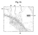
- Figure 16 shows an image of the formation of the plurality of nanotubes 94 from a top view.
- the image taken using a transmission electron microscope (TEM), has a scale bar 97 which indicates the average diameter of nanotubes 94 to be approximately 15 to 25nm.
- the individual nanoparticles 86 are not easily apparent but the agglomerated mass 98, from which the plurality of nanotubes 94 are formed, is easily distinguished.
- the image of Figure 16 is taken looking down towards the surface of the TEM grid 52 on which the nanoparticles 86 are dispersed.
- Nanotubes 94 are seen forming in directions approximately parallel a plane of the surface of the TEM grid 52. It is noted that the nanotubes 94 also may form in further directions, including a direction towards the viewer of Figure 16.
- Figure 16 illustrates the one nanoparticle 88 at the tip of each nanotube 94 and the nanotube core region 96 which is substantially hollow.
- the metallic material of the nanoparticles of the embodiments described is cobalt carbide. It is alternatively envisaged that the metallic material is substantially pure cobalt metal or a substantially pure ferromagnetic metal or a carbon alloy of a ferromagnetic metal selected from the group of metals nickel, iron, platinum and palladium. Alternatively the metallic material may be a different ferromagnetic or non-ferromagnetic metal. Further, the material forming the nanowire may be a non-metallic material, such as a semiconductor.
- the molecules are fluorocarbon decomposition products. It is alternatively envisaged that the molecules may either be different halogenated molecules or different molecules which contain carbon.
- the forming of the nanotubes as described uses molecules which are fluorocarbon decomposition products. It is envisaged that alternative halogenated molecules may be used.
- the molecules of the described embodiments are decomposition products which are provided from a polymer. It is alternatively envisaged that the molecules are not decomposition products from a polymer, but may be and are provided in a different form, for example as a gas or even a liquid. It is envisaged that further methods of forming nanoparticles may be used, for example the use of an electric arc technique in a liquid.
- the material deposited onto the surfaces of the nanoparticles is, in the described embodiments, some form of carbon. However, it is envisaged that other materials may be used to provide the material surrounding the nanowires or the material forming the nanotubes.
- the TEM grid substrate may be a different substrate and the reaction vessel and/or reagent vessels may be different in specification.
- the annealing process of the cobalt carbide nanoparticles and of the nanowires is envisaged to be different to that described.
- the temperature, reduced pressure, time period for which the process is provided, and, for the nanowire, any gas which is used to aid the process are all envisaged to be different.
- the temperature may be higher, for example approximately 700°C.
- the method of the present invention may be adapted to form nanowires or nanotubes by self-assembly methods using for example, electron lithography techniques.
- a nanowire or nanotube having the desired configuration may be readily formed on the substrate.
- An envisaged application of this method is the forming of nanowires having desired configurations on substrates, so as to form integrated electrical nanocircuits or micro electronic mechanical systems (MEMS).
- MEMS micro electronic mechanical systems
- a different envisaged application of the method of the present invention is in the production of semiconducting nanowires or nanotubes.
- the polymer which provides the decomposition products may be doped with a doping material, for example, boron or iron, such that the layer of carbon of the nanowire or the nanotube also comprises the doping material and has semiconducting properties.
- Semiconducting nanowires may be used to form nanoswitches including for example, a spin field effect transistor or a spintronic switch, which allow or prevent a flow of electrons between nanowires depending on a spin orientation of the electrons.
- a further envisaged application of the method of the present invention is in producing nanomagnetic components based on the nanowires having a permanent magnetisation along the longitudinal length. This may allow vertical recording media clusters to be produced.
Landscapes
- Chemical & Material Sciences (AREA)
- Engineering & Computer Science (AREA)
- Ceramic Engineering (AREA)
- Materials Engineering (AREA)
- Organic Chemistry (AREA)
- Manufacturing & Machinery (AREA)
- Inorganic Chemistry (AREA)
- Nanotechnology (AREA)
- Structural Engineering (AREA)
- Physics & Mathematics (AREA)
- Composite Materials (AREA)
- Condensed Matter Physics & Semiconductors (AREA)
- General Physics & Mathematics (AREA)
- Crystallography & Structural Chemistry (AREA)
- Carbon And Carbon Compounds (AREA)
- Powder Metallurgy (AREA)
- Manufacture Of Metal Powder And Suspensions Thereof (AREA)
- Compounds Of Alkaline-Earth Elements, Aluminum Or Rare-Earth Metals (AREA)
Priority Applications (1)
| Application Number | Priority Date | Filing Date | Title |
|---|---|---|---|
| EP04798395A EP1682447B1 (en) | 2003-11-07 | 2004-11-04 | Formation of metal nanowires |
Applications Claiming Priority (4)
| Application Number | Priority Date | Filing Date | Title |
|---|---|---|---|
| GB0326134A GB0326134D0 (en) | 2003-11-07 | 2003-11-07 | Forming nanostructures |
| EP03257075 | 2003-11-10 | ||
| PCT/GB2004/004670 WO2005047179A1 (en) | 2003-11-07 | 2004-11-04 | Formation of metal nanowires |
| EP04798395A EP1682447B1 (en) | 2003-11-07 | 2004-11-04 | Formation of metal nanowires |
Publications (2)
| Publication Number | Publication Date |
|---|---|
| EP1682447A1 EP1682447A1 (en) | 2006-07-26 |
| EP1682447B1 true EP1682447B1 (en) | 2007-09-12 |
Family
ID=34593645
Family Applications (1)
| Application Number | Title | Priority Date | Filing Date |
|---|---|---|---|
| EP04798395A Expired - Lifetime EP1682447B1 (en) | 2003-11-07 | 2004-11-04 | Formation of metal nanowires |
Country Status (7)
| Country | Link |
|---|---|
| US (1) | US7794784B2 (cg-RX-API-DMAC7.html) |
| EP (1) | EP1682447B1 (cg-RX-API-DMAC7.html) |
| JP (1) | JP2006516944A (cg-RX-API-DMAC7.html) |
| AT (1) | ATE372959T1 (cg-RX-API-DMAC7.html) |
| DE (1) | DE602004008958T2 (cg-RX-API-DMAC7.html) |
| ES (1) | ES2291957T3 (cg-RX-API-DMAC7.html) |
| WO (1) | WO2005047179A1 (cg-RX-API-DMAC7.html) |
Families Citing this family (30)
| Publication number | Priority date | Publication date | Assignee | Title |
|---|---|---|---|---|
| GB2427868A (en) * | 2005-07-04 | 2007-01-10 | Samuel Michael Baker | Cellulosic products having oleophobic and hydrophobic properties |
| US20100212728A1 (en) * | 2005-09-29 | 2010-08-26 | Masaru Hori | Diode and Photovoltaic Device Using Carbon Nanostructure |
| US8951632B2 (en) | 2007-01-03 | 2015-02-10 | Applied Nanostructured Solutions, Llc | CNT-infused carbon fiber materials and process therefor |
| US8158217B2 (en) | 2007-01-03 | 2012-04-17 | Applied Nanostructured Solutions, Llc | CNT-infused fiber and method therefor |
| US9005755B2 (en) | 2007-01-03 | 2015-04-14 | Applied Nanostructured Solutions, Llc | CNS-infused carbon nanomaterials and process therefor |
| US8951631B2 (en) * | 2007-01-03 | 2015-02-10 | Applied Nanostructured Solutions, Llc | CNT-infused metal fiber materials and process therefor |
| US7892956B2 (en) * | 2007-09-24 | 2011-02-22 | International Business Machines Corporation | Methods of manufacture of vertical nanowire FET devices |
| EP2398955B8 (en) | 2009-02-17 | 2020-06-03 | Applied NanoStructured Solutions, LLC | Composites comprising carbon nanotubes on fiber |
| CA2752525C (en) | 2009-02-27 | 2017-05-16 | Applied Nanostructured Solutions, Llc | Low temperature cnt growth using gas-preheat method |
| US20100224129A1 (en) | 2009-03-03 | 2010-09-09 | Lockheed Martin Corporation | System and method for surface treatment and barrier coating of fibers for in situ cnt growth |
| US9111658B2 (en) | 2009-04-24 | 2015-08-18 | Applied Nanostructured Solutions, Llc | CNS-shielded wires |
| BRPI1016242A2 (pt) | 2009-04-24 | 2016-04-26 | Applied Nanostructured Sols | material de controle de assinatura baseado em cnt. |
| CN102460447A (zh) | 2009-04-27 | 2012-05-16 | 应用纳米结构方案公司 | 防止或除去复合结构结冰的基于cnt的电阻加热 |
| WO2011017200A1 (en) | 2009-08-03 | 2011-02-10 | Lockheed Martin Corporation | Incorporation of nanoparticles in composite fibers |
| WO2011032007A1 (en) * | 2009-09-10 | 2011-03-17 | Northeastern University | Cobalt carbide-based nanoparticle permanent magnet materials |
| JP5937009B2 (ja) * | 2009-11-02 | 2016-06-22 | アプライド ナノストラクチャード ソリューションズ リミテッド ライアビリティー カンパニーApplied Nanostructured Solutions, Llc | Cnt導入アラミド繊維材料及びそのための方法 |
| US20110135491A1 (en) | 2009-11-23 | 2011-06-09 | Applied Nanostructured Solutions, Llc | Cnt-tailored composite land-based structures |
| CA2775619A1 (en) | 2009-11-23 | 2011-05-26 | Applied Nanostructured Solutions, Llc | Ceramic composite materials containing carbon nanotube-infused fiber materials and methods for production thereof |
| CN103079805B (zh) | 2009-12-14 | 2015-02-11 | 应用纳米结构方案公司 | 含有碳纳米管并入的纤维材料的防火复合材料和制品 |
| US9163354B2 (en) | 2010-01-15 | 2015-10-20 | Applied Nanostructured Solutions, Llc | CNT-infused fiber as a self shielding wire for enhanced power transmission line |
| US9167736B2 (en) | 2010-01-15 | 2015-10-20 | Applied Nanostructured Solutions, Llc | CNT-infused fiber as a self shielding wire for enhanced power transmission line |
| WO2011146151A2 (en) | 2010-02-02 | 2011-11-24 | Applied Nanostructured Solutions, Llc | Fiber containing parallel-aligned carbon nanotubes |
| BR112012021634A2 (pt) | 2010-03-02 | 2019-09-24 | Applied Nanostructured Sols | dispositivos elétricos contendo fibras de nanotubo de carbono infundidas e métodos para reprodução das mesmas. |
| JP2013521656A (ja) | 2010-03-02 | 2013-06-10 | アプライド ナノストラクチャード ソリューションズ リミテッド ライアビリティー カンパニー | カーボン・ナノチューブ浸出電極材料を含む螺旋に巻き付けられた電気機器及びその生産方法並びに生産装置 |
| US8780526B2 (en) | 2010-06-15 | 2014-07-15 | Applied Nanostructured Solutions, Llc | Electrical devices containing carbon nanotube-infused fibers and methods for production thereof |
| US9017854B2 (en) | 2010-08-30 | 2015-04-28 | Applied Nanostructured Solutions, Llc | Structural energy storage assemblies and methods for production thereof |
| CN104475313B (zh) | 2010-09-14 | 2017-05-17 | 应用奈米结构公司 | 长有碳纳米管玻璃基板及其制造方法 |
| CN103118975A (zh) | 2010-09-22 | 2013-05-22 | 应用奈米结构公司 | 具有碳纳米管成长于其上的碳纤维基板及其制造方法 |
| US9085464B2 (en) | 2012-03-07 | 2015-07-21 | Applied Nanostructured Solutions, Llc | Resistance measurement system and method of using the same |
| JP5770683B2 (ja) * | 2012-06-20 | 2015-08-26 | 日本電信電話株式会社 | カーボンナノチューブの形成方法 |
Family Cites Families (11)
| Publication number | Priority date | Publication date | Assignee | Title |
|---|---|---|---|---|
| DE68928048T2 (de) * | 1988-09-20 | 1997-11-13 | Matsushita Electric Ind Co Ltd | Verfahren zur Herstellung gebogener Graphitgegenstände |
| US6063243A (en) * | 1995-02-14 | 2000-05-16 | The Regents Of The Univeristy Of California | Method for making nanotubes and nanoparticles |
| US5780101A (en) * | 1995-02-17 | 1998-07-14 | Arizona Board Of Regents On Behalf Of The University Of Arizona | Method for producing encapsulated nanoparticles and carbon nanotubes using catalytic disproportionation of carbon monoxide |
| EP1061041A1 (en) | 1999-06-18 | 2000-12-20 | Iljin Nanotech Co., Ltd. | Low-temperature thermal chemical vapor deposition apparatus and method of synthesizing carbon nanotube using the same |
| WO2002076887A2 (en) | 2001-03-26 | 2002-10-03 | National Research Council Of Canada | Process and apparatus for synthesis of nanotubes |
| GB0111875D0 (en) | 2001-05-15 | 2001-07-04 | Univ Cambridge Tech | Synthesis of nanoscaled carbon materials |
| US7014737B2 (en) * | 2001-06-15 | 2006-03-21 | Penn State Research Foundation | Method of purifying nanotubes and nanofibers using electromagnetic radiation |
| KR100432056B1 (ko) | 2001-07-20 | 2004-05-17 | (주)케이에이치 케미컬 | 탄소나노튜브의 제조 방법 |
| NZ513637A (en) | 2001-08-20 | 2004-02-27 | Canterprise Ltd | Nanoscale electronic devices & fabrication methods |
| AU2002332622A1 (en) | 2001-08-24 | 2003-03-10 | Nano-Proprietary, Inc. | Catalyst for carbon nanotube growth |
| KR100468845B1 (ko) | 2002-01-30 | 2005-01-29 | 삼성전자주식회사 | 탄소나노튜브 제조방법 |
-
2004
- 2004-11-04 ES ES04798395T patent/ES2291957T3/es not_active Expired - Lifetime
- 2004-11-04 US US10/517,257 patent/US7794784B2/en not_active Expired - Fee Related
- 2004-11-04 WO PCT/GB2004/004670 patent/WO2005047179A1/en not_active Ceased
- 2004-11-04 AT AT04798395T patent/ATE372959T1/de not_active IP Right Cessation
- 2004-11-04 DE DE602004008958T patent/DE602004008958T2/de not_active Expired - Lifetime
- 2004-11-04 JP JP2005509253A patent/JP2006516944A/ja active Pending
- 2004-11-04 EP EP04798395A patent/EP1682447B1/en not_active Expired - Lifetime
Also Published As
| Publication number | Publication date |
|---|---|
| WO2005047179A1 (en) | 2005-05-26 |
| JP2006516944A (ja) | 2006-07-13 |
| EP1682447A1 (en) | 2006-07-26 |
| ES2291957T3 (es) | 2008-03-01 |
| US7794784B2 (en) | 2010-09-14 |
| DE602004008958T2 (de) | 2008-10-09 |
| US20050172370A1 (en) | 2005-08-04 |
| DE602004008958D1 (de) | 2007-10-25 |
| ATE372959T1 (de) | 2007-09-15 |
Similar Documents
| Publication | Publication Date | Title |
|---|---|---|
| EP1682447B1 (en) | Formation of metal nanowires | |
| US20100247752A1 (en) | Photocurable resin composition for forming overcoats rgb pixels black matrixes or spacers in color filter production, and color filters | |
| Amadi et al. | Nanoscale self-assembly: concepts, applications and challenges | |
| US7794797B2 (en) | Synthesis of carbon nanotubes by selectively heating catalyst | |
| US8663591B2 (en) | Method of preparing graphene shell and graphene shell prepared using the method | |
| Ayuk et al. | A review on synthetic methods of nanostructured materials | |
| RU2483022C2 (ru) | Способ изготовления функционализированной фуллеренами углеродной нанотрубки, композиционный материал, толстая или тонкая пленка, провод и устройство, выполненные с использованием получаемых нанотрубок | |
| Levchenko et al. | Low-temperature plasmas in carbon nanostructure synthesis | |
| US20060289351A1 (en) | Nanostructures synthesized using anodic aluminum oxide | |
| TW200540111A (en) | Process for the production of carbon nanostructure | |
| CN100503430C (zh) | 制备碳纳米细颗粒的方法和装置及单层碳纳米管 | |
| JP2009256204A (ja) | カーボンナノチューブの製造方法 | |
| Yardimci et al. | Synthesis methods of carbon nanotubes | |
| US10961123B2 (en) | Apparatus and method for synthesizing vertically aligned carbon nanotubes | |
| US7422667B1 (en) | Electrochemical deposition of carbon nanoparticles from organic solutions | |
| Kutelia et al. | Nucleation and growth of carbon nanoforms on the surface of metallic plate-substrates and the mechanism of their doping with the clusters of ferromagnetic atoms | |
| KR100658113B1 (ko) | 화학기상응축법에 의한 실리카 코팅 나노철분말 합성공정 | |
| Fang et al. | Carbon nanotubes on nanoporous alumina: from surface mats to conformal pore filling | |
| Chen et al. | The formation conditions of carbon nanotubes array based on FeNi alloy island films | |
| KR100593268B1 (ko) | 화학기상응축법에 의한 탄화물이 코팅된 철 나노분말제조공정 | |
| JP2006511422A (ja) | ナノ構造物 | |
| Matysina et al. | ELECTRIC ARC METHODS TO SYNTHESIZE CARBON NANOSTRUCTURES. | |
| JP4774994B2 (ja) | カーボンナノ構造体の製造方法、触媒金属粒子複合材料およびその製造方法 | |
| CN104785777A (zh) | 制备碳纳米管/石墨包覆的铁纳米颗粒的复合物的一种方法 | |
| Payyappilly et al. | Synthesis and Fabrication of Graphene and Reduced Graphene Oxide |
Legal Events
| Date | Code | Title | Description |
|---|---|---|---|
| PUAI | Public reference made under article 153(3) epc to a published international application that has entered the european phase |
Free format text: ORIGINAL CODE: 0009012 |
|
| 17P | Request for examination filed |
Effective date: 20060531 |
|
| AK | Designated contracting states |
Kind code of ref document: A1 Designated state(s): AT BE BG CH CY CZ DE DK EE ES FI FR GB GR HU IE IS IT LI LU MC NL PL PT RO SE SI SK TR |
|
| RIN1 | Information on inventor provided before grant (corrected) |
Inventor name: AMARATUNGA, GEHAN, ANIL, JOSEPHUNIVERSITY OF Inventor name: ANG, KHAI, HWAIB Inventor name: ALEXANDROU, IOANNISUNIVERSITY OF LIVERPOOL Inventor name: HAQ, SAJAD BAES |
|
| 17Q | First examination report despatched |
Effective date: 20060907 |
|
| DAX | Request for extension of the european patent (deleted) | ||
| GRAP | Despatch of communication of intention to grant a patent |
Free format text: ORIGINAL CODE: EPIDOSNIGR1 |
|
| GRAS | Grant fee paid |
Free format text: ORIGINAL CODE: EPIDOSNIGR3 |
|
| GRAA | (expected) grant |
Free format text: ORIGINAL CODE: 0009210 |
|
| AK | Designated contracting states |
Kind code of ref document: B1 Designated state(s): AT BE BG CH CY CZ DE DK EE ES FI FR GB GR HU IE IS IT LI LU MC NL PL PT RO SE SI SK TR |
|
| REG | Reference to a national code |
Ref country code: GB Ref legal event code: FG4D |
|
| REG | Reference to a national code |
Ref country code: CH Ref legal event code: EP |
|
| REF | Corresponds to: |
Ref document number: 602004008958 Country of ref document: DE Date of ref document: 20071025 Kind code of ref document: P |
|
| REG | Reference to a national code |
Ref country code: IE Ref legal event code: FG4D |
|
| ET | Fr: translation filed | ||
| REG | Reference to a national code |
Ref country code: SE Ref legal event code: TRGR |
|
| PG25 | Lapsed in a contracting state [announced via postgrant information from national office to epo] |
Ref country code: FI Free format text: LAPSE BECAUSE OF FAILURE TO SUBMIT A TRANSLATION OF THE DESCRIPTION OR TO PAY THE FEE WITHIN THE PRESCRIBED TIME-LIMIT Effective date: 20070912 |
|
| PG25 | Lapsed in a contracting state [announced via postgrant information from national office to epo] |
Ref country code: PL Free format text: LAPSE BECAUSE OF FAILURE TO SUBMIT A TRANSLATION OF THE DESCRIPTION OR TO PAY THE FEE WITHIN THE PRESCRIBED TIME-LIMIT Effective date: 20070912 Ref country code: CH Free format text: LAPSE BECAUSE OF FAILURE TO SUBMIT A TRANSLATION OF THE DESCRIPTION OR TO PAY THE FEE WITHIN THE PRESCRIBED TIME-LIMIT Effective date: 20070912 Ref country code: LI Free format text: LAPSE BECAUSE OF FAILURE TO SUBMIT A TRANSLATION OF THE DESCRIPTION OR TO PAY THE FEE WITHIN THE PRESCRIBED TIME-LIMIT Effective date: 20070912 Ref country code: AT Free format text: LAPSE BECAUSE OF FAILURE TO SUBMIT A TRANSLATION OF THE DESCRIPTION OR TO PAY THE FEE WITHIN THE PRESCRIBED TIME-LIMIT Effective date: 20070912 |
|
| REG | Reference to a national code |
Ref country code: ES Ref legal event code: FG2A Ref document number: 2291957 Country of ref document: ES Kind code of ref document: T3 |
|
| NLV1 | Nl: lapsed or annulled due to failure to fulfill the requirements of art. 29p and 29m of the patents act | ||
| PG25 | Lapsed in a contracting state [announced via postgrant information from national office to epo] |
Ref country code: BE Free format text: LAPSE BECAUSE OF FAILURE TO SUBMIT A TRANSLATION OF THE DESCRIPTION OR TO PAY THE FEE WITHIN THE PRESCRIBED TIME-LIMIT Effective date: 20070912 |
|
| REG | Reference to a national code |
Ref country code: CH Ref legal event code: PL |
|
| PG25 | Lapsed in a contracting state [announced via postgrant information from national office to epo] |
Ref country code: GR Free format text: LAPSE BECAUSE OF FAILURE TO SUBMIT A TRANSLATION OF THE DESCRIPTION OR TO PAY THE FEE WITHIN THE PRESCRIBED TIME-LIMIT Effective date: 20071213 Ref country code: NL Free format text: LAPSE BECAUSE OF FAILURE TO SUBMIT A TRANSLATION OF THE DESCRIPTION OR TO PAY THE FEE WITHIN THE PRESCRIBED TIME-LIMIT Effective date: 20070912 |
|
| PG25 | Lapsed in a contracting state [announced via postgrant information from national office to epo] |
Ref country code: SK Free format text: LAPSE BECAUSE OF FAILURE TO SUBMIT A TRANSLATION OF THE DESCRIPTION OR TO PAY THE FEE WITHIN THE PRESCRIBED TIME-LIMIT Effective date: 20070912 Ref country code: CZ Free format text: LAPSE BECAUSE OF FAILURE TO SUBMIT A TRANSLATION OF THE DESCRIPTION OR TO PAY THE FEE WITHIN THE PRESCRIBED TIME-LIMIT Effective date: 20070912 Ref country code: IS Free format text: LAPSE BECAUSE OF FAILURE TO SUBMIT A TRANSLATION OF THE DESCRIPTION OR TO PAY THE FEE WITHIN THE PRESCRIBED TIME-LIMIT Effective date: 20080112 Ref country code: PT Free format text: LAPSE BECAUSE OF FAILURE TO SUBMIT A TRANSLATION OF THE DESCRIPTION OR TO PAY THE FEE WITHIN THE PRESCRIBED TIME-LIMIT Effective date: 20080212 |
|
| PG25 | Lapsed in a contracting state [announced via postgrant information from national office to epo] |
Ref country code: MC Free format text: LAPSE BECAUSE OF NON-PAYMENT OF DUE FEES Effective date: 20071130 Ref country code: RO Free format text: LAPSE BECAUSE OF FAILURE TO SUBMIT A TRANSLATION OF THE DESCRIPTION OR TO PAY THE FEE WITHIN THE PRESCRIBED TIME-LIMIT Effective date: 20070912 |
|
| PLBE | No opposition filed within time limit |
Free format text: ORIGINAL CODE: 0009261 |
|
| STAA | Information on the status of an ep patent application or granted ep patent |
Free format text: STATUS: NO OPPOSITION FILED WITHIN TIME LIMIT |
|
| PG25 | Lapsed in a contracting state [announced via postgrant information from national office to epo] |
Ref country code: DE Free format text: LAPSE BECAUSE OF FAILURE TO SUBMIT A TRANSLATION OF THE DESCRIPTION OR TO PAY THE FEE WITHIN THE PRESCRIBED TIME-LIMIT Effective date: 20071213 Ref country code: DK Free format text: LAPSE BECAUSE OF FAILURE TO SUBMIT A TRANSLATION OF THE DESCRIPTION OR TO PAY THE FEE WITHIN THE PRESCRIBED TIME-LIMIT Effective date: 20070912 |
|
| 26N | No opposition filed |
Effective date: 20080613 |
|
| PG25 | Lapsed in a contracting state [announced via postgrant information from national office to epo] |
Ref country code: IE Free format text: LAPSE BECAUSE OF NON-PAYMENT OF DUE FEES Effective date: 20071105 |
|
| PG25 | Lapsed in a contracting state [announced via postgrant information from national office to epo] |
Ref country code: EE Free format text: LAPSE BECAUSE OF FAILURE TO SUBMIT A TRANSLATION OF THE DESCRIPTION OR TO PAY THE FEE WITHIN THE PRESCRIBED TIME-LIMIT Effective date: 20070912 |
|
| PG25 | Lapsed in a contracting state [announced via postgrant information from national office to epo] |
Ref country code: SI Free format text: LAPSE BECAUSE OF FAILURE TO SUBMIT A TRANSLATION OF THE DESCRIPTION OR TO PAY THE FEE WITHIN THE PRESCRIBED TIME-LIMIT Effective date: 20070912 |
|
| PG25 | Lapsed in a contracting state [announced via postgrant information from national office to epo] |
Ref country code: CY Free format text: LAPSE BECAUSE OF FAILURE TO SUBMIT A TRANSLATION OF THE DESCRIPTION OR TO PAY THE FEE WITHIN THE PRESCRIBED TIME-LIMIT Effective date: 20070912 |
|
| PG25 | Lapsed in a contracting state [announced via postgrant information from national office to epo] |
Ref country code: BG Free format text: LAPSE BECAUSE OF FAILURE TO SUBMIT A TRANSLATION OF THE DESCRIPTION OR TO PAY THE FEE WITHIN THE PRESCRIBED TIME-LIMIT Effective date: 20071212 Ref country code: LU Free format text: LAPSE BECAUSE OF NON-PAYMENT OF DUE FEES Effective date: 20071104 |
|
| PG25 | Lapsed in a contracting state [announced via postgrant information from national office to epo] |
Ref country code: TR Free format text: LAPSE BECAUSE OF FAILURE TO SUBMIT A TRANSLATION OF THE DESCRIPTION OR TO PAY THE FEE WITHIN THE PRESCRIBED TIME-LIMIT Effective date: 20070912 Ref country code: HU Free format text: LAPSE BECAUSE OF FAILURE TO SUBMIT A TRANSLATION OF THE DESCRIPTION OR TO PAY THE FEE WITHIN THE PRESCRIBED TIME-LIMIT Effective date: 20080313 |
|
| REG | Reference to a national code |
Ref country code: FR Ref legal event code: PLFP Year of fee payment: 12 |
|
| REG | Reference to a national code |
Ref country code: FR Ref legal event code: PLFP Year of fee payment: 13 |
|
| REG | Reference to a national code |
Ref country code: DE Ref legal event code: R079 Ref document number: 602004008958 Country of ref document: DE Free format text: PREVIOUS MAIN CLASS: C01B0031020000 Ipc: C01B0032050000 |
|
| PGFP | Annual fee paid to national office [announced via postgrant information from national office to epo] |
Ref country code: IT Payment date: 20161123 Year of fee payment: 13 Ref country code: SE Payment date: 20161118 Year of fee payment: 13 |
|
| REG | Reference to a national code |
Ref country code: FR Ref legal event code: PLFP Year of fee payment: 14 |
|
| PGFP | Annual fee paid to national office [announced via postgrant information from national office to epo] |
Ref country code: DE Payment date: 20171121 Year of fee payment: 14 Ref country code: FR Payment date: 20171121 Year of fee payment: 14 |
|
| PGFP | Annual fee paid to national office [announced via postgrant information from national office to epo] |
Ref country code: ES Payment date: 20171220 Year of fee payment: 14 |
|
| REG | Reference to a national code |
Ref country code: SE Ref legal event code: EUG |
|
| PG25 | Lapsed in a contracting state [announced via postgrant information from national office to epo] |
Ref country code: SE Free format text: LAPSE BECAUSE OF NON-PAYMENT OF DUE FEES Effective date: 20171105 |
|
| PG25 | Lapsed in a contracting state [announced via postgrant information from national office to epo] |
Ref country code: IT Free format text: LAPSE BECAUSE OF NON-PAYMENT OF DUE FEES Effective date: 20171104 |
|
| REG | Reference to a national code |
Ref country code: DE Ref legal event code: R119 Ref document number: 602004008958 Country of ref document: DE |
|
| PG25 | Lapsed in a contracting state [announced via postgrant information from national office to epo] |
Ref country code: DE Free format text: LAPSE BECAUSE OF FAILURE TO SUBMIT A TRANSLATION OF THE DESCRIPTION OR TO PAY THE FEE WITHIN THE PRESCRIBED TIME-LIMIT Effective date: 20190601 Ref country code: FR Free format text: LAPSE BECAUSE OF NON-PAYMENT OF DUE FEES Effective date: 20181130 |
|
| REG | Reference to a national code |
Ref country code: ES Ref legal event code: FD2A Effective date: 20200102 |
|
| PG25 | Lapsed in a contracting state [announced via postgrant information from national office to epo] |
Ref country code: ES Free format text: LAPSE BECAUSE OF NON-PAYMENT OF DUE FEES Effective date: 20181105 |
|
| PGFP | Annual fee paid to national office [announced via postgrant information from national office to epo] |
Ref country code: GB Payment date: 20191128 Year of fee payment: 16 |
|
| GBPC | Gb: european patent ceased through non-payment of renewal fee |
Effective date: 20201104 |
|
| PG25 | Lapsed in a contracting state [announced via postgrant information from national office to epo] |
Ref country code: GB Free format text: LAPSE BECAUSE OF NON-PAYMENT OF DUE FEES Effective date: 20201104 |