EP1681705A1 - Plasma processing apparatus - Google Patents
Plasma processing apparatus Download PDFInfo
- Publication number
- EP1681705A1 EP1681705A1 EP06000502A EP06000502A EP1681705A1 EP 1681705 A1 EP1681705 A1 EP 1681705A1 EP 06000502 A EP06000502 A EP 06000502A EP 06000502 A EP06000502 A EP 06000502A EP 1681705 A1 EP1681705 A1 EP 1681705A1
- Authority
- EP
- European Patent Office
- Prior art keywords
- chamber
- cathodes
- power
- branched
- cathode
- Prior art date
- Legal status (The legal status is an assumption and is not a legal conclusion. Google has not performed a legal analysis and makes no representation as to the accuracy of the status listed.)
- Withdrawn
Links
- 239000000463 material Substances 0.000 claims abstract description 33
- 239000004065 semiconductor Substances 0.000 claims description 35
- PXHVJJICTQNCMI-UHFFFAOYSA-N Nickel Chemical compound [Ni] PXHVJJICTQNCMI-UHFFFAOYSA-N 0.000 claims description 4
- 230000001360 synchronised effect Effects 0.000 claims description 3
- RYGMFSIKBFXOCR-UHFFFAOYSA-N Copper Chemical compound [Cu] RYGMFSIKBFXOCR-UHFFFAOYSA-N 0.000 claims description 2
- BQCADISMDOOEFD-UHFFFAOYSA-N Silver Chemical compound [Ag] BQCADISMDOOEFD-UHFFFAOYSA-N 0.000 claims description 2
- 229910045601 alloy Inorganic materials 0.000 claims description 2
- 239000000956 alloy Substances 0.000 claims description 2
- 229910052782 aluminium Inorganic materials 0.000 claims description 2
- XAGFODPZIPBFFR-UHFFFAOYSA-N aluminium Chemical compound [Al] XAGFODPZIPBFFR-UHFFFAOYSA-N 0.000 claims description 2
- 229910052802 copper Inorganic materials 0.000 claims description 2
- 239000010949 copper Substances 0.000 claims description 2
- PCHJSUWPFVWCPO-UHFFFAOYSA-N gold Chemical compound [Au] PCHJSUWPFVWCPO-UHFFFAOYSA-N 0.000 claims description 2
- 229910052737 gold Inorganic materials 0.000 claims description 2
- 239000010931 gold Substances 0.000 claims description 2
- 229910052751 metal Inorganic materials 0.000 claims description 2
- 239000002184 metal Substances 0.000 claims description 2
- 150000002739 metals Chemical class 0.000 claims description 2
- 229910052759 nickel Inorganic materials 0.000 claims description 2
- 229910052709 silver Inorganic materials 0.000 claims description 2
- 239000004332 silver Substances 0.000 claims description 2
- 239000000758 substrate Substances 0.000 description 35
- 238000004519 manufacturing process Methods 0.000 description 22
- 239000010408 film Substances 0.000 description 18
- 229910000838 Al alloy Inorganic materials 0.000 description 14
- 239000011521 glass Substances 0.000 description 13
- 239000010409 thin film Substances 0.000 description 10
- 238000010438 heat treatment Methods 0.000 description 9
- 239000010935 stainless steel Substances 0.000 description 8
- 229910001220 stainless steel Inorganic materials 0.000 description 7
- 230000015572 biosynthetic process Effects 0.000 description 5
- OKTJSMMVPCPJKN-UHFFFAOYSA-N Carbon Chemical compound [C] OKTJSMMVPCPJKN-UHFFFAOYSA-N 0.000 description 3
- XUIMIQQOPSSXEZ-UHFFFAOYSA-N Silicon Chemical compound [Si] XUIMIQQOPSSXEZ-UHFFFAOYSA-N 0.000 description 3
- 229910052799 carbon Inorganic materials 0.000 description 3
- 230000005284 excitation Effects 0.000 description 3
- 230000003287 optical effect Effects 0.000 description 3
- 229910052710 silicon Inorganic materials 0.000 description 3
- 239000010703 silicon Substances 0.000 description 3
- 239000000919 ceramic Substances 0.000 description 2
- 238000009413 insulation Methods 0.000 description 2
- 238000005530 etching Methods 0.000 description 1
- 230000008020 evaporation Effects 0.000 description 1
- 238000001704 evaporation Methods 0.000 description 1
- 238000000034 method Methods 0.000 description 1
- 229910001256 stainless steel alloy Inorganic materials 0.000 description 1
- 239000000126 substance Substances 0.000 description 1
Images


Classifications
-
- H—ELECTRICITY
- H01—ELECTRIC ELEMENTS
- H01J—ELECTRIC DISCHARGE TUBES OR DISCHARGE LAMPS
- H01J37/00—Discharge tubes with provision for introducing objects or material to be exposed to the discharge, e.g. for the purpose of examination or processing thereof
- H01J37/32—Gas-filled discharge tubes
- H01J37/32431—Constructional details of the reactor
Definitions
- the present invention relates to a plasma processing apparatus and a semiconductor device manufactured by the same apparatus. More particularly, the present invention relates to a plasma processing apparatus which is for use in manufacturing a semiconductor device by plasma discharge of reactive material gas in a sealable chamber, for example, by processing a substrate which is a material to be processed, and in which a plurality of pairs of cathode-anode bodies for performing plasma discharge are provided in the chamber so that a plurality of discharge spaces exist, and also relates to a semiconductor device manufactured by this plasma processing apparatus.
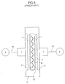
- a vertical type plasma processing apparatus shown in Fig. 4 is known in the conventional art as a semiconductor device manufacturing apparatus which is a kind of a general plasma processing apparatus.
- the semiconductor device manufacturing apparatus shown in Fig. 4 comprises a sealable vertical type chamber 3 as a reactive vessel, and one anode 4 is substantially vertically arranged with respect to a bottom surface of the chamber 3 at its inside center portion.
- the anode 4 comes in contact with a heater 5.
- the heater 5 serves to heat a glass substrate 1 (held by a substrate holding part 12), which is a material to be processed, at a constant temperature, for example, 100°C to 600°C.
- the semiconductor device manufacturing apparatus further comprises two cathodes 2, 2 which are substantially vertically arranged with respect to the bottom surface of the chamber 3 near the side wall of the inside of the chamber 3.
- the semiconductor device manufacturing apparatus will be more specifically described. That is, the anode 4 and the cathodes 2, 2 are arranged so that the anode 4 is sandwiched by the cathodes 2, 2 (in a state where two pairs of the cathode-anode bodies are placed opposite) with a predetermined interval in a horizontal direction. Then, plasma discharge is performed at spaces (two spaces) between the anode 4 and each of the cathodes 2 with reactive material gas introduced from a gas introduction pipe (not shown) into the chamber 3.
- the chamber 3 and the anode 4 use material such as stainless steel or aluminum alloy and use ceramics or the like for thermal insulation.
- Each cathode 2 is arranged so as to face the substrate 1.
- each discharge space in order that plasma discharge in each discharge space is to be the same condition by evenly supplying material gas into a plurality of (two) existing discharge spaces, it is common to provide two, the same number as that of the discharge space, power supplies 8, 8, and two matching boxes 7, 7 for matching impedance between the cathode-anode bodies and the power supplies 8, 8, and to connect each power supply 8 and matching box 7 with a power introduction wire 10.
- a power introduction wire which introduces electric power from a power supply is branched into a plurality of cathodes from one power supply in order to evenly distribute electric power from the power supply to the plurality of cathodes.
- the aforementioned conventional plasma processing apparatuses have the following problems.
- this apparatus comprises the power supply 8 and the matching box 7 for each of the two discharge spaces and each power supply 8 and matching box 7 are connected with the power introduction wire 10, it naturally becomes high cost.
- each processing needs to be the same condition with respect to two discharge spaces.
- the power supplies 8, 8 have variation of the power supply itself, true input power is not necessarily the same even when power values are set to be the same. Therefore, this apparatus is required to perform adjustment according to the respective discharge spaces, control for individual discharge is very complicated, and there is a problem in that variation occurs readily at each discharge.
- the number of the power introduction wire from the power supply to the cathode is set to be 1/2 of that of the discharge spaces. It is assumed herein that a homogeneous film is produced between the surfaces of the cathode and the anode by plasma discharge.
- the present invention has been devised in view of such circumstances, and it is an object of the present invention to provide a simply configured plasma processing apparatus which can equally introduce reactive material gas into a plurality of discharge spaces for performing plasma discharge by the reactive material gas inside the chamber, and a semiconductor device manufactured by this plasma processing apparatus.
- a plasma processing apparatus comprising : a sealable chamber to be introduced with reactive material gas; a plurality of pairs of cathode-anode bodies arranged in the chamber, for forming a plurality of discharge spaces for performing plasma discharge of the material gas; a power supply for plasma discharge, placed outside the chamber; a matching box placed outside the chamber, for matching impedance between the cathode-anode bodies and the power supply; and a power introduction wire extending to each of the cathodes from the power supply via the matching box, wherein the power introduction wire is branched to the number corresponding to the number of the cathodes between the matching box and the cathodes, and the branched wires are symmetrically extended.
- a plasma processing apparatus comprising: a sealable chamber to be introduced with reactive material gas; 2 n pairs (n is an integer of one or more) of cathode-anode bodies arranged in the chamber, for forming 2 n discharge spaces for performing plasma discharge of the material gas; 2 m (m is an integer smaller than n) power supplies for plasma discharge, placed outside the chamber; 2 m matching boxes placed outside the chamber, for matching impedance between the cathode-anode bodies and the power supplies; and a power introduction wire extending to each of the cathodes from the power supplies via the matching boxes, wherein the power supplies are synchronized with each other, and the power introduction wire is branched into two wires between the matching box and the cathodes, and the branched wires are symmetrically extended.
- a plasma processing apparatus comprising : a sealable chamber to be introduced with reactive material gas; a plurality of pairs of cathode-anode bodies arranged in the chamber, for forming a plurality of discharge spaces for performing plasma discharge of the material gas; a power supply for plasma discharge, placed outside the chamber; and a power introduction wire extending to each of the cathodes from the power supply, wherein the power introduction wire is branched to the number corresponding to the number of the cathodes between the power supply and the cathodes, and the branched wires are symmetrically extended.
- a semiconductor device manufactured by the plasma processing apparatus according to any one of the aforementioned aspects of the present invention.
- a power introduction wire extending from a power supply to each cathode via a matching box is branched to the number corresponding to the number of the cathodes between the matching box and the cathodes and the branched wires are symmetrically extended, electric power can be evenly supplied to a plurality of discharge spaces in the chamber without providing a special adjustment mechanism.
- a power introduction wire extending from the power supplies to each cathode via 2 m matching boxes is branched into two wires between the matching box and the cathodes and the branched wires are symmetrically extended, electric power can be evenly supplied to a plurality of discharge spaces in the chamber without providing a special adjustment mechanism.
- a power introduction wire extending from a power supply to each cathode is branched to the number corresponding to the number of the cathodes between the power supply and the cathodes and the branched wires are symmetrically extended, electric power can be evenly supplied to a plurality of discharge spaces in the chamber without providing a special adjustment mechanism.
- the semiconductor device since there is used a plasma processing apparatus in which electric power can be evenly supplied to a plurality of discharge spaces in the chamber without providing a special adjustment mechanism, a low cost semiconductor device can be manufactured with little variation in quality.
- the plurality of pairs of cathode-anode bodies may be composed of four pairs of cathode-anode bodies, and the power introduction wire may be branched into two wires between the matching box and the cathodes, and then the branched wires may be further branched into two wires.
- the power introduction wire may be branched into two wires between the matching box and the cathodes, and then the branched wires may be further branched into two wires.
- the plurality of pairs of cathode-anode bodies may be composed of 2 n pairs (n is an integer of one or more) of cathode-anode bodies, and the power introduction wire may be branched into 2 n wires between the matching box and the cathodes.
- the power introduction wire may be accommodated in a housing arranged for every branched part between the matching box and the chamber.
- the power supply operates at a frequency from 1 MHz or more to 60 MHz or less.
- electric power can be supplied to a large cathode having a size of several meters, irrespective of the shape of the cathode which inputs electric power.
- the power introduction wire is made of copper, aluminum, nickel, silver, gold, or an alloy primarily composed of these metals. This power introduction wire can sufficiently respond to the increase of impedance caused by lengthened wire due to performing a plurality of branches.
- Fig. 1 is a schematic longitudinal sectional view showing a semiconductor device manufacturing apparatus as a plasma processing apparatus according to a first embodiment.
- an anode 4 and cathodes 2, 2 are arranged so that the anode 4 is sandwiched by the cathodes 2, 2 with a predetermined interval in a horizontal direction. Then, plasma discharge is performed at spaces (two discharge spaces) between the anode 4 and each of the cathodes 2, 2 with reactive material gas introduced into a chamber 3.
- the semiconductor device manufacturing apparatus comprises the chamber 3 which is sealable vertical type as a reactive vessel, and one anode 4 is substantially vertically arranged with respect to a bottom surface of the chamber 3 at its inside center portion. Glass substrates 1, 1, which are materials to be processed, are arranged on both sides of the anode 4.
- the chamber 3 uses stainless steel, aluminum alloy, or the like and uses ceramics or the like for thermal insulation. Further, in the chamber 3, the cathodes 2, 2 are arranged so to face the substrates 1, 1, respectively.
- the anode 4 is made of material having conductivity and heat resistance, such as stainless steel, aluminum alloy, and carbon.
- the substrates 1, 1 generally use a silicon substrate, a glass substrate, or the like; however, it is not limited to these substrates.
- glass substrates 1, 1 are used.
- the anode 4 has dimensions suitably determined in accordance with those of the glass substrates 1, 1 for forming a thin film.
- the anode 4 is designed to be dimensions in 1000 to 1500 mm x 600 to 1000 mm with respect to those of the substrates 1, 1, 900 to 1200 mm x 400 to 900 mm.
- the anode 4 incorporates a heater 5 which performs control for heating the anode 4 to be the room temperature to 300°C.
- the anode 4 uses a heater which incorporates an encapsulated type heating device such as a sheathed heater and an encapsulated type temperature sensor such as a thermocouple in an aluminum alloy, and the heater performs control for heating the anode to be the room temperature to 300°C.
- the cathodes 2, 2 are made of stainless steel, aluminum alloy, or the like. Here, aluminum alloy is used. Dimensions of the cathode 2 are set to suitable values in accordance with those of the substrate 1 which performs film formation. Here, it is designed in 1000 to 1500 mm x 600 to 1000 mm.
- Electric power is supplied to the cathodes 2, 2 by one plasma excitation power supply 8.
- the power supply 8 uses an AC electric power of 10 W to 100 kW at a frequency of 1.00 MHz to 60 MHz.
- the power supply uses 10 W to 10 kW at 13.56 MHz to 60 MHz.
- One matching box 7 is arranged between the power supply 8 and the chamber 3 for matching impedance between the cathode-anode bodies 2, 4 and the power supply 8.
- the power supply 8 and the matching box 7 are connected with one power introduction wire 10.
- the power introduction wire 10 is branched into two wires between the matching box 7 and the cathodes 2 and the branched wires are symmetrically extended (horizontal line symmetry in Fig. 1) in order to evenly supply electric power from the power supply 8 to a plurality of (two) discharge spaces in the semiconductor device manufacturing apparatus.
- the electric power is inputted to each cathode 2 via a plurality of power introduction terminals provided on cathode connection parts. Since respective distances of the power introduction wire 10 from the branched part to the cathode connection parts are configured so as to be the same distance, interconnection impedance becomes the same, so that the electric power is equally divided.
- the power introduction wire 10 between the matching box 7 and the chamber 3 is accommodated in one housing 6 placed between the matching box 7 and the chamber 3.
- material gas is filled into a clearance between the cathodes 2, 2 and the anode 4 at a predetermined flow rate and pressure and high frequency power is applied to the cathodes 2, 2 and the anode 4, thereby generating a glow discharge region (plasma discharge region) between the cathodes 2, 2 and the anode 4. Then, an amorphous film or a crystalline film can be formed on the surfaces of the substrates 1, 1.
- the power introduction wire 10 for introducing from one power supply 8 to each of the cathodes 2, 2 is branched into two wires between the matching box 7 and the cathodes 2, 2, and the branched wires are further symmetrically extended from the branched part to the cathodes 2, 2.
- the power introduction wire 10 is accommodated in the housing 6 between the matching box 7 and the chamber, probability of occurring of mutual interference between the branched power introduction wires 10 can be prevented.
- Fig. 2 is a schematic longitudinal sectional view showing a semiconductor device manufacturing apparatus as a plasma processing apparatus according to a second embodiment.
- a sealable chamber 3 In a sealable chamber 3, four pairs of cathode-anode bodies 2, 4 are substantially vertically arranged with respect to a bottom surface of the chamber 3. Then, plasma discharge is performed at spaces (four discharge spaces) between the anodes 4 and the cathodes 2 with reactive material gas introduced into the chamber 3.
- the cathode-anode bodies 2, 4 are made up of four pairs for simplification in Fig. 2; however, it is not limited to this.
- the anode 4 is made of material having conductivity and heat resistance, such as stainless steel, aluminum alloy, and carbon.
- a glass substrate 1 which is a material to be processed is arranged on the left side of each anode 4.
- the substrate 1 generally uses a silicon substrate, a glass substrate, or the like; however, it is not limited to these substrates.
- a glass substrate 1 is used.
- the anode 4 has dimensions suitably determined in accordance with those of the glass substrates 1 for forming a thin film.
- the anode 4 is designed to be dimensions in 1000 to 1500 mm x 600 to 1000 mm with respect to those of the substrate 1, 900 to 1200 mm x 400 to 900 mm.
- the anode 4 incorporates a heater 5 which performs control for heating the anode 4 to be the room temperature to 300°C.
- the anode 4 uses a heater which incorporates an encapsulated type heating device such as a sheathed heater and an encapsulated type temperature sensor such as a thermocouple in an aluminum alloy, the heater performs control for heating the anode between the room temperature and 300°C.
- the cathodes 2 are made of stainless steel, aluminum alloy, or the like. Here, aluminum alloy is used. Dimensions of the cathode 2 are set to suitable values in accordance with those of the substrate 1 which performs film formation. Here, it is designed in 1000 to 1500 mm x 600 to 1000 mm.
- Electric power is supplied to the cathodes 2 by one plasma excitation power supply 8.
- the power supply 8 uses an AC electric power of 10 W to 100 kW at a frequency of 1.00 MHz to 60 MHz.
- the power supply uses 10 W to 10 kW at 13.56 MHz to 60 MHz.
- One matching box 7 is arranged between the power supply 8 and the chamber 3 for matching impedance between the cathode-anode bodies 2, 4 and the power supply 8.
- the power supply 8 and the matching box 7 are connected with one power introduction wire 10.
- the power introduction wire 10 is branched into two wires between the matching box 7 and the chamber 3, and then, further similarly branched into two wires.
- the branched wires are symmetrically extended (horizontal line symmetry in Fig. 2).
- the electric power is inputted to each cathode 2 via a plurality of power introduction terminals provided on cathode connection parts. Since respective distances of the power introduction wire 10 from the branched part to the cathode connection parts are configured so as to be the same distance, interconnection impedance becomes the same, so that the electric power is equally divided.
- the power introduction wire 10 between the matching box 7 and the chamber 3 is accommodated in three small and large housings 6 disposed between the matching box 7 and the chamber 3.
- interconnection impedance can be the same by conforming capacitance of the power introduction wire 10.
- material gas is filled into a clearance between the cathode 2 and the anode 4 at a predetermined flow rate and pressure and high frequency power is applied to the cathode 2 and the anode 4, thereby generating a glow discharge region (plasma discharge region) between the cathode 2 and the anode 4. Then, an amorphous film or a crystalline film can be formed on the surface of the substrate 1.
- the power introduction wire 10 for introducing from one power supply 8 to each cathode 2 is branched into two wires between the matching box 7 and the cathodes 2, and then, the respective branched wires are further branched into two wires and symmetrically extended from the branched part to the cathodes 2.
- the power introduction wires 10 are accommodated in three housing 6 between the matching box 7 and the chamber 3, probability of occurring of mutual interference between the branched power introduction wires 10 can be prevented.
- Fig. 3 is a schematic longitudinal sectional view showing a semiconductor device manufacturing apparatus as a plasma processing apparatus according to a third embodiment.
- a sealable chamber 3 In a sealable chamber 3, four pairs of cathode-anode bodies 2, 4 are substantially vertically arranged with respect to a bottom surface of the chamber 3. Then, plasma discharge is performed at spaces (four discharge spaces) between the anodes 4 and the cathodes 2 with reactive material gas introduced into the chamber 3.
- the cathode-anode bodies 2, 4 are made up of four pairs for simplification in Fig. 3; however, it is not limited to this.
- the anode 4 is made of material having conductivity and heat resistance, such as stainless steel, aluminum alloy, and carbon.
- a glass substrate 1 which is a material to be processed is arranged on the left side of each anode 4.
- the substrate 1 generally uses a silicon substrate, a glass substrate, or the like; however, it is not limited to these substrates.
- a glass substrate 1 is used.
- the anode 4 has dimensions suitably determined in accordance with those of the glass substrates 1 for forming a thin film.
- the anode 4 is designed to be dimensions in 1000 to 1500 mm x 600 to 1000 mm with respect to those of the substrates 1, 900 to 1200 mm x 400 to 900 mm.
- the anode 4 incorporates a heater 5 which performs control for heating the anode 4 to be the room temperature to 300°C.
- the anode 4 uses a heater which incorporates an encapsulated type heating device such as a sheathed heater and an encapsulated type temperature sensor such as a thermocouple in an aluminum alloy, the heater performs control for heating the anode between the room temperature and 300°C.
- the cathodes 2 are made of stainless steel, aluminum alloy, or the like. Here, aluminum alloy is used. Dimensions of the cathode 2 are set to suitable values in accordance with those of the substrate 1 which performs film formation. Here, it is designed in 1000 to 1500 mm x 600 to 1000 mm.
- Electric power is supplied to the cathodes 2 by two plasma excitation power supplies 9.
- Each power supply 9 uses an AC electric power of 10 W to 100 kW at a frequency of 1.00 MHz to 60 MHz.
- the power supply uses 10 W to 10 kW at 13.56 MHz to 60 MHz.
- each power introduction wire 10 is branched into two wires between the matching box 7 and the cathode 2.
- the branched wires are symmetrically extended (horizontal line symmetry in Fig. 3).
- Two power supplies 9, 9 share a high frequency generator 11 which is provided between the power supplies 9, 9 and synchronize the amplitudes of the respective power supplies 9, 9.
- the power introduction wire 10 between each matching box 7 and the chamber 3 is accommodated in one housing 6 which is arranged between each matching box 7 and the chamber 3 in order to conform interconnection impedance of each electric power wire.
- the interconnection impedance can be the same by conforming interconnection capacitance and electric power can be supplied without occurring of interference between the power supplies 9, 9.
- the electric power is inputted to each cathode 2 via a plurality of power introduction terminals. Since respective distances from the branched part to the cathode connection parts are the same, the interconnection impedance becomes the same. Consequently, the electric power is equally divided.
- reactive gas is filled into a clearance between the cathode 2 and the anode 4 at a predetermined flow rate and pressure and high frequency power is applied to the cathode 2 and the anode 4, thereby generating a glow discharge region (plasma discharge region) between the cathode 2 and the anode 4.
- a glow discharge region plasma discharge region
- an amorphous film or a crystalline film can be formed on the surface of the substrate 1. Furthermore, since the film formed in each discharge space is the same film formation speed and the same film quality, it can be concluded that equivalent discharge spaces can be formed.
- the power introduction wire 10 for introducing from two power supplies 9, 9 to respective cathodes 2 is branched into two wires between the respective matching boxes 7 and the cathodes 2 and is symmetrically extended from the branched part to the cathodes 2.
- the power introduction wires 10 are accommodated in the housing 6 between each matching box 7 and the chamber 3, probability of occurring of mutual interference between the power supplies 9, 9 and between the branched power introduction wires 10 can be prevented.
Landscapes
- Physics & Mathematics (AREA)
- Engineering & Computer Science (AREA)
- Plasma & Fusion (AREA)
- Chemical & Material Sciences (AREA)
- Analytical Chemistry (AREA)
- Chemical Vapour Deposition (AREA)
- Plasma Technology (AREA)
- Photovoltaic Devices (AREA)
Abstract
Description
- The present invention relates to a plasma processing apparatus and a semiconductor device manufactured by the same apparatus. More particularly, the present invention relates to a plasma processing apparatus which is for use in manufacturing a semiconductor device by plasma discharge of reactive material gas in a sealable chamber, for example, by processing a substrate which is a material to be processed, and in which a plurality of pairs of cathode-anode bodies for performing plasma discharge are provided in the chamber so that a plurality of discharge spaces exist, and also relates to a semiconductor device manufactured by this plasma processing apparatus.
- A vertical type plasma processing apparatus shown in Fig. 4 is known in the conventional art as a semiconductor device manufacturing apparatus which is a kind of a general plasma processing apparatus.
- The semiconductor device manufacturing apparatus shown in Fig. 4 comprises a sealable
vertical type chamber 3 as a reactive vessel, and oneanode 4 is substantially vertically arranged with respect to a bottom surface of thechamber 3 at its inside center portion. Theanode 4 comes in contact with aheater 5. Theheater 5 serves to heat a glass substrate 1 (held by a substrate holding part 12), which is a material to be processed, at a constant temperature, for example, 100°C to 600°C. The semiconductor device manufacturing apparatus further comprises twocathodes chamber 3 near the side wall of the inside of thechamber 3. - The semiconductor device manufacturing apparatus will be more specifically described. That is, the
anode 4 and thecathodes anode 4 is sandwiched by thecathodes 2, 2 (in a state where two pairs of the cathode-anode bodies are placed opposite) with a predetermined interval in a horizontal direction. Then, plasma discharge is performed at spaces (two spaces) between theanode 4 and each of thecathodes 2 with reactive material gas introduced from a gas introduction pipe (not shown) into thechamber 3. - The
chamber 3 and theanode 4 use material such as stainless steel or aluminum alloy and use ceramics or the like for thermal insulation. Eachcathode 2 is arranged so as to face thesubstrate 1. - In the semiconductor device manufacturing apparatus, in order that plasma discharge in each discharge space is to be the same condition by evenly supplying material gas into a plurality of (two) existing discharge spaces, it is common to provide two, the same number as that of the discharge space,
power supplies matching boxes power supplies power supply 8 and matchingbox 7 with apower introduction wire 10. - In addition, as for a conventional plasma processing apparatus, those which improve etching or evaporation uniformity in a plasma chemical technology are known (see, for example, US Patent No. 4,264,393).
- In an apparatus disclosed in US Patent No. 4,264,393, a power introduction wire which introduces electric power from a power supply is branched into a plurality of cathodes from one power supply in order to evenly distribute electric power from the power supply to the plurality of cathodes.
- The aforementioned conventional plasma processing apparatuses have the following problems.
- First, the apparatus shown in Fig. 4 will be described. Since this apparatus comprises the
power supply 8 and the matchingbox 7 for each of the two discharge spaces and eachpower supply 8 andmatching box 7 are connected with thepower introduction wire 10, it naturally becomes high cost. - In addition, in the case where parallel processing is performed, each processing needs to be the same condition with respect to two discharge spaces. However, since the
power supplies - Next, the apparatus disclosed in US Patent No. 4,264,393 will be described. In this apparatus, the number of the power introduction wire from the power supply to the cathode is set to be 1/2 of that of the discharge spaces. It is assumed herein that a homogeneous film is produced between the surfaces of the cathode and the anode by plasma discharge.
- However, actually, it is well known that a cathode film obtained by the plasma processing apparatus is inferior in quality compared to an anode film.
- If considering the case where electric power is supplied to each cathode with a power introduction wire branched from one power supply, not only a branching filter is required at every branched point in order to evenly distribute electric power by such a branch method, but also the power introduction wire from the power supply to each cathode differs largely in length.
- Consequently, even if power coaxial cable whose impedance is constant is used, considerable variation can be expected in electric power to be supplied to each cathode. As a result, the apparatus in which parallel processing is assumed to be performed has very large variation in every branch.
- The present invention has been devised in view of such circumstances, and it is an object of the present invention to provide a simply configured plasma processing apparatus which can equally introduce reactive material gas into a plurality of discharge spaces for performing plasma discharge by the reactive material gas inside the chamber, and a semiconductor device manufactured by this plasma processing apparatus.
- According to one aspect of the present invention, there is provided a plasma processing apparatus comprising : a sealable chamber to be introduced with reactive material gas; a plurality of pairs of cathode-anode bodies arranged in the chamber, for forming a plurality of discharge spaces for performing plasma discharge of the material gas; a power supply for plasma discharge, placed outside the chamber; a matching box placed outside the chamber, for matching impedance between the cathode-anode bodies and the power supply; and a power introduction wire extending to each of the cathodes from the power supply via the matching box, wherein the power introduction wire is branched to the number corresponding to the number of the cathodes between the matching box and the cathodes, and the branched wires are symmetrically extended.
- According to another aspect of the present invention, there is provided a plasma processing apparatus comprising: a sealable chamber to be introduced with reactive material gas; 2n pairs (n is an integer of one or more) of cathode-anode bodies arranged in the chamber, for forming 2n discharge spaces for performing plasma discharge of the material gas; 2m (m is an integer smaller than n) power supplies for plasma discharge, placed outside the chamber; 2m matching boxes placed outside the chamber, for matching impedance between the cathode-anode bodies and the power supplies; and a power introduction wire extending to each of the cathodes from the power supplies via the matching boxes, wherein the power supplies are synchronized with each other, and the power introduction wire is branched into two wires between the matching box and the cathodes, and the branched wires are symmetrically extended.
- According to still another aspect of the present invention, there is provided a plasma processing apparatus comprising : a sealable chamber to be introduced with reactive material gas; a plurality of pairs of cathode-anode bodies arranged in the chamber, for forming a plurality of discharge spaces for performing plasma discharge of the material gas; a power supply for plasma discharge, placed outside the chamber; and a power introduction wire extending to each of the cathodes from the power supply, wherein the power introduction wire is branched to the number corresponding to the number of the cathodes between the power supply and the cathodes, and the branched wires are symmetrically extended.
- According to yet another aspect of the present invention, there is provided a semiconductor device manufactured by the plasma processing apparatus according to any one of the aforementioned aspects of the present invention.
-
- Fig. 1 is a schematic longitudinal sectional view showing a plasma processing apparatus (one power supply and two branches) according to a first embodiment of the present invention;
- Fig. 2 is a schematic longitudinal sectional view showing a plasma processing apparatus (one power supply and four branches) according to a second embodiment of the present invention;
- Fig. 3 is a schematic longitudinal sectional view showing a plasma processing apparatus (two power supplies and two branches) according to a third embodiment of the present invention; and
- Fig. 4 is a schematic longitudinal sectional view showing a conventional general semiconductor device manufacturing apparatus.
- In the plasma processing apparatus according to one aspect of the present invention, since a power introduction wire extending from a power supply to each cathode via a matching box is branched to the number corresponding to the number of the cathodes between the matching box and the cathodes and the branched wires are symmetrically extended, electric power can be evenly supplied to a plurality of discharge spaces in the chamber without providing a special adjustment mechanism.
- In the plasma processing apparatus according to another aspect of the present invention, since 2m power supplies are synchronized with each other, a power introduction wire extending from the power supplies to each cathode via 2m matching boxes is branched into two wires between the matching box and the cathodes and the branched wires are symmetrically extended, electric power can be evenly supplied to a plurality of discharge spaces in the chamber without providing a special adjustment mechanism.
- In the plasma processing apparatus according to still another aspect of the present invention, since a power introduction wire extending from a power supply to each cathode is branched to the number corresponding to the number of the cathodes between the power supply and the cathodes and the branched wires are symmetrically extended, electric power can be evenly supplied to a plurality of discharge spaces in the chamber without providing a special adjustment mechanism.
- In the semiconductor device according to yet another aspect of the present invention, since there is used a plasma processing apparatus in which electric power can be evenly supplied to a plurality of discharge spaces in the chamber without providing a special adjustment mechanism, a low cost semiconductor device can be manufactured with little variation in quality.
- In the plasma processing apparatus according to the present invention, for example, the plurality of pairs of cathode-anode bodies may be composed of four pairs of cathode-anode bodies, and the power introduction wire may be branched into two wires between the matching box and the cathodes, and then the branched wires may be further branched into two wires. With this configuration, electric power can be evenly supplied to the four discharge spaces in the chamber without providing a special adjustment mechanism.
- In the plasma processing apparatus according to the present invention, for example, the plurality of pairs of cathode-anode bodies may be composed of 2n pairs (n is an integer of one or more) of cathode-anode bodies, and the power introduction wire may be branched into 2n wires between the matching box and the cathodes. With this configuration, electric power can be evenly supplied to the 2n discharge spaces in the chamber without providing a special adjustment mechanism.
- In the plasma processing apparatus according to the present invention, for example, the power introduction wire may be accommodated in a housing arranged for every branched part between the matching box and the chamber. With this configuration, probability of occurring of mutual interference between branched power introduction wires can be prevented in the case where one power supply is provided. Further, probability of occurring of mutual interference between the power supplies and between the branched power introduction wires can be prevented in the case where a plurality of power supplies are provided.
- In the plasma processing apparatus according to the present invention, preferably, the power supply operates at a frequency from 1 MHz or more to 60 MHz or less. With this power supply, electric power can be supplied to a large cathode having a size of several meters, irrespective of the shape of the cathode which inputs electric power.
- In the plasma processing apparatus according to the present invention, preferably, the power introduction wire is made of copper, aluminum, nickel, silver, gold, or an alloy primarily composed of these metals. This power introduction wire can sufficiently respond to the increase of impedance caused by lengthened wire due to performing a plurality of branches.
- The present invention will be described below based on three embodiments showing a plasma processing apparatus. It is to be noted that the present invention is not limited to these embodiments. First Embodiment
- Fig. 1 is a schematic longitudinal sectional view showing a semiconductor device manufacturing apparatus as a plasma processing apparatus according to a first embodiment.
- In the semiconductor device manufacturing apparatus, an
anode 4 andcathodes anode 4 is sandwiched by thecathodes anode 4 and each of thecathodes chamber 3. - The semiconductor device manufacturing apparatus will be more specifically described. That is, the semiconductor device manufacturing apparatus comprises the
chamber 3 which is sealable vertical type as a reactive vessel, and oneanode 4 is substantially vertically arranged with respect to a bottom surface of thechamber 3 at its inside center portion.Glass substrates anode 4. - The
chamber 3 uses stainless steel, aluminum alloy, or the like and uses ceramics or the like for thermal insulation. Further, in thechamber 3, thecathodes substrates anode 4 is made of material having conductivity and heat resistance, such as stainless steel, aluminum alloy, and carbon. - The
substrates glass substrates anode 4 has dimensions suitably determined in accordance with those of theglass substrates anode 4 is designed to be dimensions in 1000 to 1500 mm x 600 to 1000 mm with respect to those of thesubstrates - The
anode 4 incorporates aheater 5 which performs control for heating theanode 4 to be the room temperature to 300°C. Here, theanode 4 uses a heater which incorporates an encapsulated type heating device such as a sheathed heater and an encapsulated type temperature sensor such as a thermocouple in an aluminum alloy, and the heater performs control for heating the anode to be the room temperature to 300°C. - The
cathodes cathode 2 are set to suitable values in accordance with those of thesubstrate 1 which performs film formation. Here, it is designed in 1000 to 1500 mm x 600 to 1000 mm. - Electric power is supplied to the
cathodes excitation power supply 8. Thepower supply 8 uses an AC electric power of 10 W to 100 kW at a frequency of 1.00 MHz to 60 MHz. - Here, the power supply uses 10 W to 10 kW at 13.56 MHz to 60 MHz.
- One
matching box 7 is arranged between thepower supply 8 and thechamber 3 for matching impedance between the cathode-anode bodies power supply 8. Thepower supply 8 and thematching box 7 are connected with onepower introduction wire 10. - The
power introduction wire 10 is branched into two wires between thematching box 7 and thecathodes 2 and the branched wires are symmetrically extended (horizontal line symmetry in Fig. 1) in order to evenly supply electric power from thepower supply 8 to a plurality of (two) discharge spaces in the semiconductor device manufacturing apparatus. - After branching, the electric power is inputted to each
cathode 2 via a plurality of power introduction terminals provided on cathode connection parts. Since respective distances of thepower introduction wire 10 from the branched part to the cathode connection parts are configured so as to be the same distance, interconnection impedance becomes the same, so that the electric power is equally divided. Here, thepower introduction wire 10 between thematching box 7 and thechamber 3 is accommodated in onehousing 6 placed between thematching box 7 and thechamber 3. - In the semiconductor device manufacturing apparatus as configured above, material gas is filled into a clearance between the
cathodes anode 4 at a predetermined flow rate and pressure and high frequency power is applied to thecathodes anode 4, thereby generating a glow discharge region (plasma discharge region) between thecathodes anode 4. Then, an amorphous film or a crystalline film can be formed on the surfaces of thesubstrates - Furthermore, since the films formed in the respective discharge spaces have the same film formation speed and the same film quality, it can be concluded that equivalent discharge spaces are formed.
- In the semiconductor device manufacturing apparatus according to the first embodiment as configured above, there are two discharge spaces in one
chamber 3, thepower introduction wire 10 for introducing from onepower supply 8 to each of thecathodes matching box 7 and thecathodes cathodes - Consequently, electric power can be evenly supplied to two discharge spaces without providing a special adjustment mechanism, whereby a semiconductor device such as a solar cell using a semiconductor thin film or an optical thin film, a thin film transistor (TFT), a photosensitive member can be efficiently obtained at low cost.
- Since the
power introduction wire 10 is accommodated in thehousing 6 between thematching box 7 and the chamber, probability of occurring of mutual interference between the branchedpower introduction wires 10 can be prevented. - Fig. 2 is a schematic longitudinal sectional view showing a semiconductor device manufacturing apparatus as a plasma processing apparatus according to a second embodiment.
- In a
sealable chamber 3, four pairs of cathode-anode bodies chamber 3. Then, plasma discharge is performed at spaces (four discharge spaces) between theanodes 4 and thecathodes 2 with reactive material gas introduced into thechamber 3. The cathode-anode bodies anode 4 is made of material having conductivity and heat resistance, such as stainless steel, aluminum alloy, and carbon. - A
glass substrate 1 which is a material to be processed is arranged on the left side of eachanode 4. Thesubstrate 1 generally uses a silicon substrate, a glass substrate, or the like; however, it is not limited to these substrates. Here, aglass substrate 1 is used. - The
anode 4 has dimensions suitably determined in accordance with those of theglass substrates 1 for forming a thin film. Here, theanode 4 is designed to be dimensions in 1000 to 1500 mm x 600 to 1000 mm with respect to those of thesubstrate 1, 900 to 1200 mm x 400 to 900 mm. - The
anode 4 incorporates aheater 5 which performs control for heating theanode 4 to be the room temperature to 300°C. Here, theanode 4 uses a heater which incorporates an encapsulated type heating device such as a sheathed heater and an encapsulated type temperature sensor such as a thermocouple in an aluminum alloy, the heater performs control for heating the anode between the room temperature and 300°C. - The
cathodes 2 are made of stainless steel, aluminum alloy, or the like. Here, aluminum alloy is used. Dimensions of thecathode 2 are set to suitable values in accordance with those of thesubstrate 1 which performs film formation. Here, it is designed in 1000 to 1500 mm x 600 to 1000 mm. - Electric power is supplied to the
cathodes 2 by one plasmaexcitation power supply 8. Thepower supply 8 uses an AC electric power of 10 W to 100 kW at a frequency of 1.00 MHz to 60 MHz. Here, the power supply uses 10 W to 10 kW at 13.56 MHz to 60 MHz. - One
matching box 7 is arranged between thepower supply 8 and thechamber 3 for matching impedance between the cathode-anode bodies power supply 8. Thepower supply 8 and thematching box 7 are connected with onepower introduction wire 10. - In order to evenly supply electric power from the
power supply 8 to a plurality of (four) discharge spaces in the semiconductor device manufacturing apparatus, thepower introduction wire 10 is branched into two wires between thematching box 7 and thechamber 3, and then, further similarly branched into two wires. The branched wires are symmetrically extended (horizontal line symmetry in Fig. 2). - After branching, the electric power is inputted to each
cathode 2 via a plurality of power introduction terminals provided on cathode connection parts. Since respective distances of thepower introduction wire 10 from the branched part to the cathode connection parts are configured so as to be the same distance, interconnection impedance becomes the same, so that the electric power is equally divided. Here, thepower introduction wire 10 between thematching box 7 and thechamber 3 is accommodated in three small andlarge housings 6 disposed between thematching box 7 and thechamber 3. - With this configuration, interconnection impedance can be the same by conforming capacitance of the
power introduction wire 10. - In the semiconductor device manufacturing apparatus according to the second embodiment as configured above, material gas is filled into a clearance between the
cathode 2 and theanode 4 at a predetermined flow rate and pressure and high frequency power is applied to thecathode 2 and theanode 4, thereby generating a glow discharge region (plasma discharge region) between thecathode 2 and theanode 4. Then, an amorphous film or a crystalline film can be formed on the surface of thesubstrate 1. - Furthermore, according to the semiconductor device manufacturing apparatus, there are four discharge spaces in one
chamber 3, thepower introduction wire 10 for introducing from onepower supply 8 to eachcathode 2 is branched into two wires between thematching box 7 and thecathodes 2, and then, the respective branched wires are further branched into two wires and symmetrically extended from the branched part to thecathodes 2. - Consequently, electric power can be evenly supplied to four discharge spaces without providing a special adjustment mechanism, whereby a semiconductor device such as a solar cell using a semiconductor thin film or an optical thin film, a TFT, a photosensitive member can be efficiently obtained at low cost.
- Further, since the
power introduction wires 10 are accommodated in threehousing 6 between thematching box 7 and thechamber 3, probability of occurring of mutual interference between the branchedpower introduction wires 10 can be prevented. - Fig. 3 is a schematic longitudinal sectional view showing a semiconductor device manufacturing apparatus as a plasma processing apparatus according to a third embodiment.
- In a
sealable chamber 3, four pairs of cathode-anode bodies chamber 3. Then, plasma discharge is performed at spaces (four discharge spaces) between theanodes 4 and thecathodes 2 with reactive material gas introduced into thechamber 3. The cathode-anode bodies anode 4 is made of material having conductivity and heat resistance, such as stainless steel, aluminum alloy, and carbon. - A
glass substrate 1 which is a material to be processed is arranged on the left side of eachanode 4. Thesubstrate 1 generally uses a silicon substrate, a glass substrate, or the like; however, it is not limited to these substrates. Here, aglass substrate 1 is used. - The
anode 4 has dimensions suitably determined in accordance with those of theglass substrates 1 for forming a thin film. Here, theanode 4 is designed to be dimensions in 1000 to 1500 mm x 600 to 1000 mm with respect to those of thesubstrates 1, 900 to 1200 mm x 400 to 900 mm. - The
anode 4 incorporates aheater 5 which performs control for heating theanode 4 to be the room temperature to 300°C. Here, theanode 4 uses a heater which incorporates an encapsulated type heating device such as a sheathed heater and an encapsulated type temperature sensor such as a thermocouple in an aluminum alloy, the heater performs control for heating the anode between the room temperature and 300°C. - The
cathodes 2 are made of stainless steel, aluminum alloy, or the like. Here, aluminum alloy is used. Dimensions of thecathode 2 are set to suitable values in accordance with those of thesubstrate 1 which performs film formation. Here, it is designed in 1000 to 1500 mm x 600 to 1000 mm. - Electric power is supplied to the
cathodes 2 by two plasma excitation power supplies 9. Eachpower supply 9 uses an AC electric power of 10 W to 100 kW at a frequency of 1.00 MHz to 60 MHz. Here, the power supply uses 10 W to 10 kW at 13.56 MHz to 60 MHz. - Two (2n (n is an integer of one or more) and when n = 1) matching
boxes 7 are arranged between thepower supplies chamber 3 for matching impedance between the cathode-anode bodies power supplies power supply 9 and thematching box 7 are connected with onepower introduction wire 10. - In order to evenly supply electric power from the
power supplies power introduction wire 10 is branched into two wires between thematching box 7 and thecathode 2. The branched wires are symmetrically extended (horizontal line symmetry in Fig. 3). - Two
power supplies high frequency generator 11 which is provided between thepower supplies respective power supplies power introduction wire 10 between eachmatching box 7 and thechamber 3 is accommodated in onehousing 6 which is arranged between eachmatching box 7 and thechamber 3 in order to conform interconnection impedance of each electric power wire. With this configuration, the interconnection impedance can be the same by conforming interconnection capacitance and electric power can be supplied without occurring of interference between thepower supplies - After branching, the electric power is inputted to each
cathode 2 via a plurality of power introduction terminals. Since respective distances from the branched part to the cathode connection parts are the same, the interconnection impedance becomes the same. Consequently, the electric power is equally divided. - In the semiconductor device manufacturing apparatus as configured above, reactive gas is filled into a clearance between the
cathode 2 and theanode 4 at a predetermined flow rate and pressure and high frequency power is applied to thecathode 2 and theanode 4, thereby generating a glow discharge region (plasma discharge region) between thecathode 2 and theanode 4. Then, an amorphous film or a crystalline film can be formed on the surface of thesubstrate 1. Furthermore, since the film formed in each discharge space is the same film formation speed and the same film quality, it can be concluded that equivalent discharge spaces can be formed. - According to the semiconductor device manufacturing apparatus according to the third embodiment as configured above, there are four discharge spaces in one
chamber 3, and thepower introduction wire 10 for introducing from twopower supplies respective cathodes 2 is branched into two wires between therespective matching boxes 7 and thecathodes 2 and is symmetrically extended from the branched part to thecathodes 2. - Consequently, electric power can be evenly supplied to four discharge spaces without providing a special adjustment mechanism, whereby a semiconductor device such as a solar cell using a semiconductor thin film or an optical thin film, a TFT, a photosensitive member can be efficiently obtained at low cost.
- Further, since the
power introduction wires 10 are accommodated in thehousing 6 between eachmatching box 7 and thechamber 3, probability of occurring of mutual interference between thepower supplies power introduction wires 10 can be prevented.
Claims (9)
- A plasma processing apparatus comprising: a sealable chamber to be introduced with reactive material gas; a plurality of pairs of cathode-anode bodies arranged in the chamber, for forming a plurality of discharge spaces for performing plasma discharge of the material gas; a power supply for plasma discharge, placed outside the chamber; a matching box placed outside the chamber, for matching impedance between the cathode-anode bodies and the power supply; and a power introduction wire extending to each of the cathodes from the power supply via the matching box, wherein
the power introduction wire is branched to the number corresponding to the number of the cathodes between the matching box and the cathodes, and the branched wires are symmetrically extended. - The plasma processing apparatus according to claim 1, wherein the plurality of pairs of cathode-anode bodies are composed of four pairs of cathode-anode bodies, and the power introduction wire is branched into two wires between the matching box and the cathodes, and then the branched wires are further branched into two wires.
- The plasma processing apparatus according to claim 1, wherein the plurality of pairs of cathode-anode bodies are composed of 2n pairs (n is an integer of one or more) of cathode-anode bodies, and the power introduction wire is branched into 2n wires between the matching box and the cathodes.
- A plasma processing apparatus comprising: a sealable chamber to be introduced with reactive material gas; 2n pairs (n is an integer of one or more) of cathode-anode bodies arranged in the chamber, for forming 2n discharge spaces for performing plasma discharge of the material gas; 2m (m is an integer smaller than n) power supplies for plasma discharge, placed outside the chamber; 2m matching boxes placed outside the chamber, for matching impedance between the cathode-anode bodies and the power supplies; and a power introduction wire extending to each of the cathodes from the power supplies via the matching boxes, wherein
the power supplies are synchronized with each other, and the power introduction wire is branched into two wires between the matching box and the cathodes, and the branched wires are symmetrically extended. - The plasma processing apparatus according to claim 1 or claim 4, wherein the power introduction wire is accommodated in a housing arranged for every branched part between the matching box and the chamber.
- The plasma processing apparatus according to claim 1 or claim 4, wherein the power supply operates at a frequency from 1 MHz or more to 60 MHz or less.
- The plasma processing apparatus according to claim 1 or claim 4, wherein the power introduction wire is made of copper, aluminum, nickel, silver, gold, or an alloy primarily composed of these metals.
- A plasma processing apparatus comprising: a sealable chamber to be introduced with reactive material gas; a plurality of pairs of cathode-anode bodies arranged in the chamber, for forming a plurality of discharge spaces for performing plasma discharge of the material gas; a power supply for plasma discharge, placed outside the chamber; and a power introduction wire extending to each of the cathodes from the power supply, wherein
the power introduction wire is branched to the number corresponding to the number of the cathodes between the power supply and the cathodes, and the branched wires are symmetrically extended. - A semiconductor device manufactured by the plasma processing apparatus according to claim 1, claim 4 or claim 8.
Applications Claiming Priority (1)
| Application Number | Priority Date | Filing Date | Title |
|---|---|---|---|
| JP2005006605A JP2006196681A (en) | 2005-01-13 | 2005-01-13 | Plasma processing apparatus and semiconductor device manufactured by the same |
Publications (1)
| Publication Number | Publication Date |
|---|---|
| EP1681705A1 true EP1681705A1 (en) | 2006-07-19 |
Family
ID=36123172
Family Applications (1)
| Application Number | Title | Priority Date | Filing Date |
|---|---|---|---|
| EP06000502A Withdrawn EP1681705A1 (en) | 2005-01-13 | 2006-01-11 | Plasma processing apparatus |
Country Status (3)
| Country | Link |
|---|---|
| US (1) | US7540257B2 (en) |
| EP (1) | EP1681705A1 (en) |
| JP (1) | JP2006196681A (en) |
Families Citing this family (19)
| Publication number | Priority date | Publication date | Assignee | Title |
|---|---|---|---|---|
| JP2004288984A (en) * | 2003-03-24 | 2004-10-14 | Sharp Corp | Film forming apparatus and film forming method |
| JP4185483B2 (en) * | 2004-10-22 | 2008-11-26 | シャープ株式会社 | Plasma processing equipment |
| KR101353684B1 (en) * | 2006-11-14 | 2014-01-20 | 엘지전자 주식회사 | Apparatus and method for generation a plasma |
| JP5039576B2 (en) * | 2008-01-11 | 2012-10-03 | シャープ株式会社 | Plasma processing equipment |
| JP4558067B2 (en) * | 2008-05-21 | 2010-10-06 | シャープ株式会社 | Plasma processing equipment |
| US20110312167A1 (en) * | 2008-06-02 | 2011-12-22 | Katsushi Kishimoto | Plasma processing apparatus, and deposition method an etching method using the plasma processing apparatus |
| KR101627297B1 (en) * | 2008-10-13 | 2016-06-03 | 한국에이에스엠지니텍 주식회사 | Plasma processing member, deposition apparatus including the same and depositing method using the same |
| US20110300694A1 (en) * | 2008-11-12 | 2011-12-08 | Ulvac, Inc. | Electrode circuit, film formation device, electrode unit, and film formation method |
| JP4852653B2 (en) * | 2010-03-15 | 2012-01-11 | シャープ株式会社 | Plasma processing apparatus, plasma processing method, and semiconductor device manufacturing method |
| JP4887440B2 (en) * | 2010-04-20 | 2012-02-29 | シャープ株式会社 | Plasma processing apparatus, plasma processing method, and semiconductor device manufacturing method |
| US20120164834A1 (en) * | 2010-12-22 | 2012-06-28 | Kevin Jennings | Variable-Density Plasma Processing of Semiconductor Substrates |
| CN102652946A (en) * | 2011-03-04 | 2012-09-05 | 富葵精密组件(深圳)有限公司 | Plasma cleaning device and plasma cleaning method |
| JP2013004172A (en) * | 2011-06-10 | 2013-01-07 | Tokyo Electron Ltd | High-frequency power distribution device, and substrate processing device using the same |
| JP5787712B2 (en) * | 2011-10-20 | 2015-09-30 | 株式会社日立製作所 | Plasma processing equipment |
| US9088085B2 (en) | 2012-09-21 | 2015-07-21 | Novellus Systems, Inc. | High temperature electrode connections |
| WO2015108528A1 (en) * | 2014-01-17 | 2015-07-23 | Seagate Technology Llc | Etching source installable in a storage medium processing tool |
| US10438805B2 (en) | 2016-12-06 | 2019-10-08 | Tokyo Electron Limited | Methods and systems for chamber matching and monitoring |
| CN215925072U (en) * | 2020-09-24 | 2022-03-01 | 株式会社国际电气 | Substrate processing apparatus |
| US12542256B2 (en) * | 2022-11-21 | 2026-02-03 | Applied Materials, Inc. | Batch processing chambers for plasma-enhanced deposition |
Citations (4)
| Publication number | Priority date | Publication date | Assignee | Title |
|---|---|---|---|---|
| US4664890A (en) * | 1984-06-22 | 1987-05-12 | Kanegafuchi Kagaku Kogyo Kabushiki Kaisha | Glow-discharge decomposition apparatus |
| US4887005A (en) * | 1987-09-15 | 1989-12-12 | Rough J Kirkwood H | Multiple electrode plasma reactor power distribution system |
| EP0689226A1 (en) * | 1994-06-21 | 1995-12-27 | The Boc Group, Inc. | Multiple electrode plasma reactor |
| US5958141A (en) * | 1995-11-06 | 1999-09-28 | Sanyo Vacuum Industries Co., Ltd. | Dry etching device |
Family Cites Families (37)
| Publication number | Priority date | Publication date | Assignee | Title |
|---|---|---|---|---|
| US4264393A (en) * | 1977-10-31 | 1981-04-28 | Motorola, Inc. | Reactor apparatus for plasma etching or deposition |
| JPS54106081A (en) | 1978-02-08 | 1979-08-20 | Hitachi Ltd | Growth method in vapor phase |
| JPS5846057B2 (en) * | 1979-03-19 | 1983-10-14 | 富士通株式会社 | Plasma treatment method |
| US4287851A (en) | 1980-01-16 | 1981-09-08 | Dozier Alfred R | Mounting and excitation system for reaction in the plasma state |
| US4381965A (en) * | 1982-01-06 | 1983-05-03 | Drytek, Inc. | Multi-planar electrode plasma etching |
| JPS60624U (en) | 1983-06-15 | 1985-01-07 | 菊水電子工業株式会社 | electronic load device |
| JPS6025235A (en) | 1983-07-22 | 1985-02-08 | Hitachi Ltd | Etching device |
| US4825806A (en) * | 1984-02-17 | 1989-05-02 | Kanegafuchi Kagaku Kogyo Kabushiki Kaisha | Film forming apparatus |
| JPH0644554B2 (en) * | 1984-03-28 | 1994-06-08 | 株式会社富士電機総合研究所 | Plasma CVD equipment |
| US5061359A (en) * | 1985-01-17 | 1991-10-29 | International Business Machines Corporation | Plasma processing apparatus including three bus structures |
| JPS61214513A (en) | 1985-03-20 | 1986-09-24 | Hitachi Ltd | processing equipment |
| US4676865A (en) * | 1986-02-07 | 1987-06-30 | Delarge Richard S | Plasma desmear/etchback system and method of use |
| JPH01173711A (en) * | 1987-12-28 | 1989-07-10 | Shimadzu Corp | Thin film forming device |
| JPH01305513A (en) * | 1988-06-03 | 1989-12-08 | Nec Corp | Plasma cvd apparatus |
| US5041201A (en) * | 1988-09-16 | 1991-08-20 | Semiconductor Energy Laboratory Co., Ltd. | Plasma processing method and apparatus |
| DE69032952T2 (en) | 1989-11-15 | 1999-09-30 | Haruhisa Kinoshita | Dry treatment device |
| JP2628404B2 (en) | 1990-10-25 | 1997-07-09 | 日亜化学工業株式会社 | Semiconductor crystal film growth method |
| US5082547A (en) * | 1991-02-01 | 1992-01-21 | Plasma Etch | Plasma etching reactor |
| JPH05209279A (en) * | 1991-10-29 | 1993-08-20 | Canon Inc | Metal film forming apparatus and metal film forming method |
| CH687986A5 (en) * | 1993-05-03 | 1997-04-15 | Balzers Hochvakuum | Plasma treatment equipment and method for its operation. |
| JPH08172054A (en) * | 1994-12-19 | 1996-07-02 | Mitsubishi Electric Corp | Plasma CVD method, apparatus therefor, and method of manufacturing semiconductor device using the same |
| JPH08279495A (en) | 1995-02-07 | 1996-10-22 | Seiko Epson Corp | Plasma processing apparatus and method |
| JPH0950992A (en) | 1995-08-04 | 1997-02-18 | Sharp Corp | Film forming equipment |
| TW340957B (en) | 1996-02-01 | 1998-09-21 | Canon Hanbai Kk | Plasma processor and gas release device |
| JP2975885B2 (en) | 1996-02-01 | 1999-11-10 | キヤノン販売株式会社 | Gas disperser and plasma processing device |
| JP3844274B2 (en) * | 1998-06-25 | 2006-11-08 | 独立行政法人産業技術総合研究所 | Plasma CVD apparatus and plasma CVD method |
| US6349670B1 (en) * | 1998-11-30 | 2002-02-26 | Alps Electric Co., Ltd. | Plasma treatment equipment |
| JP2000294511A (en) | 1999-04-09 | 2000-10-20 | Ftl:Kk | Manufacture for semiconductor device |
| JP3969907B2 (en) | 1999-09-14 | 2007-09-05 | 松下電器産業株式会社 | Plasma processing equipment |
| US6821379B2 (en) | 2001-12-21 | 2004-11-23 | The Procter & Gamble Company | Portable apparatus and method for treating a workpiece |
| US20030164143A1 (en) | 2002-01-10 | 2003-09-04 | Hitachi Kokusai Electric Inc. | Batch-type remote plasma processing apparatus |
| JP2004022638A (en) * | 2002-06-13 | 2004-01-22 | Toppan Printing Co Ltd | Plasma processing equipment |
| JP2004259853A (en) | 2003-02-25 | 2004-09-16 | Kanegafuchi Chem Ind Co Ltd | Apparatus and method for manufacturing crystalline silicon-based thin film photoelectric conversion device |
| JP2004288984A (en) | 2003-03-24 | 2004-10-14 | Sharp Corp | Film forming apparatus and film forming method |
| KR20060115734A (en) | 2003-10-28 | 2006-11-09 | 노드슨 코포레이션 | Plasma Processing System and Plasma Processing Method |
| JP4185483B2 (en) | 2004-10-22 | 2008-11-26 | シャープ株式会社 | Plasma processing equipment |
| JP4584722B2 (en) | 2005-01-13 | 2010-11-24 | シャープ株式会社 | Plasma processing apparatus and semiconductor device manufactured by the same |
-
2005
- 2005-01-13 JP JP2005006605A patent/JP2006196681A/en active Pending
-
2006
- 2006-01-10 US US11/328,448 patent/US7540257B2/en not_active Expired - Fee Related
- 2006-01-11 EP EP06000502A patent/EP1681705A1/en not_active Withdrawn
Patent Citations (4)
| Publication number | Priority date | Publication date | Assignee | Title |
|---|---|---|---|---|
| US4664890A (en) * | 1984-06-22 | 1987-05-12 | Kanegafuchi Kagaku Kogyo Kabushiki Kaisha | Glow-discharge decomposition apparatus |
| US4887005A (en) * | 1987-09-15 | 1989-12-12 | Rough J Kirkwood H | Multiple electrode plasma reactor power distribution system |
| EP0689226A1 (en) * | 1994-06-21 | 1995-12-27 | The Boc Group, Inc. | Multiple electrode plasma reactor |
| US5958141A (en) * | 1995-11-06 | 1999-09-28 | Sanyo Vacuum Industries Co., Ltd. | Dry etching device |
Also Published As
| Publication number | Publication date |
|---|---|
| US20060151319A1 (en) | 2006-07-13 |
| US7540257B2 (en) | 2009-06-02 |
| JP2006196681A (en) | 2006-07-27 |
Similar Documents
| Publication | Publication Date | Title |
|---|---|---|
| US7540257B2 (en) | Plasma processing apparatus and semiconductor device manufactured by the same apparatus | |
| JP4185483B2 (en) | Plasma processing equipment | |
| TW201704563A (en) | Crystal boat and wafer processing device | |
| US8092640B2 (en) | Plasma processing apparatus and semiconductor device manufactured by the same apparatus | |
| TW201706445A (en) | Crystal boat, wafer processing device, and wafer processing method | |
| JP2010225296A (en) | Inductively coupled antenna unit and plasma processing apparatus | |
| WO2009142138A1 (en) | Plasma processing apparatus | |
| US7722738B2 (en) | Semiconductor device manufacturing unit and semiconductor device manufacturing method | |
| JP4936297B2 (en) | Plasma processing apparatus, plasma processing method, and semiconductor device | |
| JP5329796B2 (en) | Plasma processing equipment | |
| CN101336467B (en) | Plasma processing device and plasma processing method | |
| JP4982577B2 (en) | Plasma processing apparatus and semiconductor device manufactured by the same | |
| JPS63190173A (en) | Plasma treating device | |
| KR101358858B1 (en) | Electrostatic chuck apparatus and substrate processing equipment having the same | |
| JP4890313B2 (en) | Plasma CVD equipment | |
| JP4421864B2 (en) | Thin film manufacturing apparatus and thin film manufacturing method using the apparatus | |
| WO2010016423A1 (en) | Dielectric window, dielectric window manufacturing method, and plasma treatment apparatus | |
| JP4290207B2 (en) | Semiconductor element manufacturing apparatus and semiconductor element manufacturing method | |
| JPWO2009147993A1 (en) | Plasma processing apparatus, film forming method and etching method using the same | |
| CN108140528A (en) | Plasma processing equipment for wafers | |
| KR20090073271A (en) | Substrate processing chamber with capacitively coupled electrodes with laser beam | |
| JPS6058617A (en) | plasma processing equipment |
Legal Events
| Date | Code | Title | Description |
|---|---|---|---|
| PUAI | Public reference made under article 153(3) epc to a published international application that has entered the european phase |
Free format text: ORIGINAL CODE: 0009012 |
|
| AK | Designated contracting states |
Kind code of ref document: A1 Designated state(s): AT BE BG CH CY CZ DE DK EE ES FI FR GB GR HU IE IS IT LI LT LU LV MC NL PL PT RO SE SI SK TR |
|
| AX | Request for extension of the european patent |
Extension state: AL BA HR MK YU |
|
| 17P | Request for examination filed |
Effective date: 20061018 |
|
| 17Q | First examination report despatched |
Effective date: 20061006 |
|
| AKX | Designation fees paid |
Designated state(s): DE ES GB IT |
|
| STAA | Information on the status of an ep patent application or granted ep patent |
Free format text: STATUS: THE APPLICATION IS DEEMED TO BE WITHDRAWN |
|
| 18D | Application deemed to be withdrawn |
Effective date: 20150130 |