EP1677360A2 - Semiconductor device and fabrication method thereof - Google Patents
Semiconductor device and fabrication method thereof Download PDFInfo
- Publication number
- EP1677360A2 EP1677360A2 EP05007947A EP05007947A EP1677360A2 EP 1677360 A2 EP1677360 A2 EP 1677360A2 EP 05007947 A EP05007947 A EP 05007947A EP 05007947 A EP05007947 A EP 05007947A EP 1677360 A2 EP1677360 A2 EP 1677360A2
- Authority
- EP
- European Patent Office
- Prior art keywords
- mixed crystal
- sige mixed
- silicon substrate
- regions
- type
- Prior art date
- Legal status (The legal status is an assumption and is not a legal conclusion. Google has not performed a legal analysis and makes no representation as to the accuracy of the status listed.)
- Granted
Links
Images







Classifications
-
- H—ELECTRICITY
- H10—SEMICONDUCTOR DEVICES; ELECTRIC SOLID-STATE DEVICES NOT OTHERWISE PROVIDED FOR
- H10D—INORGANIC ELECTRIC SEMICONDUCTOR DEVICES
- H10D30/00—Field-effect transistors [FET]
- H10D30/60—Insulated-gate field-effect transistors [IGFET]
- H10D30/791—Arrangements for exerting mechanical stress on the crystal lattice of the channel regions
-
- H—ELECTRICITY
- H10—SEMICONDUCTOR DEVICES; ELECTRIC SOLID-STATE DEVICES NOT OTHERWISE PROVIDED FOR
- H10D—INORGANIC ELECTRIC SEMICONDUCTOR DEVICES
- H10D30/00—Field-effect transistors [FET]
- H10D30/01—Manufacture or treatment
- H10D30/021—Manufacture or treatment of FETs having insulated gates [IGFET]
- H10D30/0212—Manufacture or treatment of FETs having insulated gates [IGFET] using self-aligned silicidation
-
- H—ELECTRICITY
- H10—SEMICONDUCTOR DEVICES; ELECTRIC SOLID-STATE DEVICES NOT OTHERWISE PROVIDED FOR
- H10D—INORGANIC ELECTRIC SEMICONDUCTOR DEVICES
- H10D30/00—Field-effect transistors [FET]
- H10D30/01—Manufacture or treatment
- H10D30/021—Manufacture or treatment of FETs having insulated gates [IGFET]
- H10D30/027—Manufacture or treatment of FETs having insulated gates [IGFET] of lateral single-gate IGFETs
- H10D30/0275—Manufacture or treatment of FETs having insulated gates [IGFET] of lateral single-gate IGFETs forming single crystalline semiconductor source or drain regions resulting in recessed gates, e.g. forming raised source or drain regions
-
- H—ELECTRICITY
- H10—SEMICONDUCTOR DEVICES; ELECTRIC SOLID-STATE DEVICES NOT OTHERWISE PROVIDED FOR
- H10D—INORGANIC ELECTRIC SEMICONDUCTOR DEVICES
- H10D30/00—Field-effect transistors [FET]
- H10D30/60—Insulated-gate field-effect transistors [IGFET]
-
- H—ELECTRICITY
- H10—SEMICONDUCTOR DEVICES; ELECTRIC SOLID-STATE DEVICES NOT OTHERWISE PROVIDED FOR
- H10D—INORGANIC ELECTRIC SEMICONDUCTOR DEVICES
- H10D30/00—Field-effect transistors [FET]
- H10D30/60—Insulated-gate field-effect transistors [IGFET]
- H10D30/601—Insulated-gate field-effect transistors [IGFET] having lightly-doped drain or source extensions, e.g. LDD IGFETs or DDD IGFETs
-
- H—ELECTRICITY
- H10—SEMICONDUCTOR DEVICES; ELECTRIC SOLID-STATE DEVICES NOT OTHERWISE PROVIDED FOR
- H10D—INORGANIC ELECTRIC SEMICONDUCTOR DEVICES
- H10D30/00—Field-effect transistors [FET]
- H10D30/60—Insulated-gate field-effect transistors [IGFET]
- H10D30/791—Arrangements for exerting mechanical stress on the crystal lattice of the channel regions
- H10D30/797—Arrangements for exerting mechanical stress on the crystal lattice of the channel regions being in source or drain regions, e.g. SiGe source or drain
-
- H—ELECTRICITY
- H10—SEMICONDUCTOR DEVICES; ELECTRIC SOLID-STATE DEVICES NOT OTHERWISE PROVIDED FOR
- H10D—INORGANIC ELECTRIC SEMICONDUCTOR DEVICES
- H10D62/00—Semiconductor bodies, or regions thereof, of devices having potential barriers
- H10D62/01—Manufacture or treatment
- H10D62/021—Forming source or drain recesses by etching e.g. recessing by etching and then refilling
-
- H—ELECTRICITY
- H10—SEMICONDUCTOR DEVICES; ELECTRIC SOLID-STATE DEVICES NOT OTHERWISE PROVIDED FOR
- H10D—INORGANIC ELECTRIC SEMICONDUCTOR DEVICES
- H10D62/00—Semiconductor bodies, or regions thereof, of devices having potential barriers
- H10D62/10—Shapes, relative sizes or dispositions of the regions of the semiconductor bodies; Shapes of the semiconductor bodies
- H10D62/113—Isolations within a component, i.e. internal isolations
- H10D62/115—Dielectric isolations, e.g. air gaps
- H10D62/116—Dielectric isolations, e.g. air gaps adjoining the input or output regions of field-effect devices, e.g. adjoining source or drain regions
-
- H—ELECTRICITY
- H10—SEMICONDUCTOR DEVICES; ELECTRIC SOLID-STATE DEVICES NOT OTHERWISE PROVIDED FOR
- H10D—INORGANIC ELECTRIC SEMICONDUCTOR DEVICES
- H10D62/00—Semiconductor bodies, or regions thereof, of devices having potential barriers
- H10D62/10—Shapes, relative sizes or dispositions of the regions of the semiconductor bodies; Shapes of the semiconductor bodies
- H10D62/13—Semiconductor regions connected to electrodes carrying current to be rectified, amplified or switched, e.g. source or drain regions
- H10D62/149—Source or drain regions of field-effect devices
- H10D62/151—Source or drain regions of field-effect devices of IGFETs
-
- H—ELECTRICITY
- H10—SEMICONDUCTOR DEVICES; ELECTRIC SOLID-STATE DEVICES NOT OTHERWISE PROVIDED FOR
- H10D—INORGANIC ELECTRIC SEMICONDUCTOR DEVICES
- H10D62/00—Semiconductor bodies, or regions thereof, of devices having potential barriers
- H10D62/40—Crystalline structures
- H10D62/405—Orientations of crystalline planes
-
- H—ELECTRICITY
- H10—SEMICONDUCTOR DEVICES; ELECTRIC SOLID-STATE DEVICES NOT OTHERWISE PROVIDED FOR
- H10D—INORGANIC ELECTRIC SEMICONDUCTOR DEVICES
- H10D62/00—Semiconductor bodies, or regions thereof, of devices having potential barriers
- H10D62/80—Semiconductor bodies, or regions thereof, of devices having potential barriers characterised by the materials
- H10D62/82—Heterojunctions
- H10D62/822—Heterojunctions comprising only Group IV materials heterojunctions, e.g. Si/Ge heterojunctions
-
- H—ELECTRICITY
- H10—SEMICONDUCTOR DEVICES; ELECTRIC SOLID-STATE DEVICES NOT OTHERWISE PROVIDED FOR
- H10D—INORGANIC ELECTRIC SEMICONDUCTOR DEVICES
- H10D64/00—Electrodes of devices having potential barriers
- H10D64/01—Manufacture or treatment
- H10D64/011—Manufacture or treatment of electrodes ohmically coupled to a semiconductor
- H10D64/0111—Manufacture or treatment of electrodes ohmically coupled to a semiconductor to Group IV semiconductors
- H10D64/0112—Manufacture or treatment of electrodes ohmically coupled to a semiconductor to Group IV semiconductors using conductive layers comprising silicides
-
- H—ELECTRICITY
- H10—SEMICONDUCTOR DEVICES; ELECTRIC SOLID-STATE DEVICES NOT OTHERWISE PROVIDED FOR
- H10D—INORGANIC ELECTRIC SEMICONDUCTOR DEVICES
- H10D64/00—Electrodes of devices having potential barriers
- H10D64/60—Electrodes characterised by their materials
- H10D64/62—Electrodes ohmically coupled to a semiconductor
-
- H—ELECTRICITY
- H10—SEMICONDUCTOR DEVICES; ELECTRIC SOLID-STATE DEVICES NOT OTHERWISE PROVIDED FOR
- H10D—INORGANIC ELECTRIC SEMICONDUCTOR DEVICES
- H10D64/00—Electrodes of devices having potential barriers
- H10D64/60—Electrodes characterised by their materials
- H10D64/66—Electrodes having a conductor capacitively coupled to a semiconductor by an insulator, e.g. MIS electrodes
- H10D64/667—Electrodes having a conductor capacitively coupled to a semiconductor by an insulator, e.g. MIS electrodes the conductor comprising a layer of alloy material, compound material or organic material contacting the insulator, e.g. TiN workfunction layers
- H10D64/668—Electrodes having a conductor capacitively coupled to a semiconductor by an insulator, e.g. MIS electrodes the conductor comprising a layer of alloy material, compound material or organic material contacting the insulator, e.g. TiN workfunction layers the layer being a silicide, e.g. TiSi2
-
- H—ELECTRICITY
- H10—SEMICONDUCTOR DEVICES; ELECTRIC SOLID-STATE DEVICES NOT OTHERWISE PROVIDED FOR
- H10D—INORGANIC ELECTRIC SEMICONDUCTOR DEVICES
- H10D64/00—Electrodes of devices having potential barriers
- H10D64/60—Electrodes characterised by their materials
- H10D64/66—Electrodes having a conductor capacitively coupled to a semiconductor by an insulator, e.g. MIS electrodes
- H10D64/68—Electrodes having a conductor capacitively coupled to a semiconductor by an insulator, e.g. MIS electrodes characterised by the insulator, e.g. by the gate insulator
- H10D64/693—Electrodes having a conductor capacitively coupled to a semiconductor by an insulator, e.g. MIS electrodes characterised by the insulator, e.g. by the gate insulator the insulator comprising nitrogen, e.g. nitrides, oxynitrides or nitrogen-doped materials
-
- H—ELECTRICITY
- H10—SEMICONDUCTOR DEVICES; ELECTRIC SOLID-STATE DEVICES NOT OTHERWISE PROVIDED FOR
- H10P—GENERIC PROCESSES OR APPARATUS FOR THE MANUFACTURE OR TREATMENT OF DEVICES COVERED BY CLASS H10
- H10P14/00—Formation of materials, e.g. in the shape of layers or pillars
- H10P14/20—Formation of materials, e.g. in the shape of layers or pillars of semiconductor materials
- H10P14/24—Formation of materials, e.g. in the shape of layers or pillars of semiconductor materials using chemical vapour deposition [CVD]
-
- H—ELECTRICITY
- H10—SEMICONDUCTOR DEVICES; ELECTRIC SOLID-STATE DEVICES NOT OTHERWISE PROVIDED FOR
- H10P—GENERIC PROCESSES OR APPARATUS FOR THE MANUFACTURE OR TREATMENT OF DEVICES COVERED BY CLASS H10
- H10P14/00—Formation of materials, e.g. in the shape of layers or pillars
- H10P14/20—Formation of materials, e.g. in the shape of layers or pillars of semiconductor materials
- H10P14/27—Formation of materials, e.g. in the shape of layers or pillars of semiconductor materials using selective deposition, e.g. simultaneous growth of monocrystalline and non-monocrystalline semiconductor materials
- H10P14/271—Formation of materials, e.g. in the shape of layers or pillars of semiconductor materials using selective deposition, e.g. simultaneous growth of monocrystalline and non-monocrystalline semiconductor materials characterised by the preparation of substrate for selective deposition
-
- H—ELECTRICITY
- H10—SEMICONDUCTOR DEVICES; ELECTRIC SOLID-STATE DEVICES NOT OTHERWISE PROVIDED FOR
- H10P—GENERIC PROCESSES OR APPARATUS FOR THE MANUFACTURE OR TREATMENT OF DEVICES COVERED BY CLASS H10
- H10P14/00—Formation of materials, e.g. in the shape of layers or pillars
- H10P14/20—Formation of materials, e.g. in the shape of layers or pillars of semiconductor materials
- H10P14/29—Formation of materials, e.g. in the shape of layers or pillars of semiconductor materials characterised by the substrates
- H10P14/2901—Materials
- H10P14/2902—Materials being Group IVA materials
- H10P14/2905—Silicon, silicon germanium or germanium
-
- H—ELECTRICITY
- H10—SEMICONDUCTOR DEVICES; ELECTRIC SOLID-STATE DEVICES NOT OTHERWISE PROVIDED FOR
- H10P—GENERIC PROCESSES OR APPARATUS FOR THE MANUFACTURE OR TREATMENT OF DEVICES COVERED BY CLASS H10
- H10P14/00—Formation of materials, e.g. in the shape of layers or pillars
- H10P14/20—Formation of materials, e.g. in the shape of layers or pillars of semiconductor materials
- H10P14/34—Deposited materials, e.g. layers
- H10P14/3402—Deposited materials, e.g. layers characterised by the chemical composition
- H10P14/3404—Deposited materials, e.g. layers characterised by the chemical composition being Group IVA materials
- H10P14/3411—Silicon, silicon germanium or germanium
-
- H—ELECTRICITY
- H10—SEMICONDUCTOR DEVICES; ELECTRIC SOLID-STATE DEVICES NOT OTHERWISE PROVIDED FOR
- H10P—GENERIC PROCESSES OR APPARATUS FOR THE MANUFACTURE OR TREATMENT OF DEVICES COVERED BY CLASS H10
- H10P14/00—Formation of materials, e.g. in the shape of layers or pillars
- H10P14/20—Formation of materials, e.g. in the shape of layers or pillars of semiconductor materials
- H10P14/34—Deposited materials, e.g. layers
- H10P14/3438—Doping during depositing
- H10P14/3441—Conductivity type
- H10P14/3444—P-type
-
- H—ELECTRICITY
- H10—SEMICONDUCTOR DEVICES; ELECTRIC SOLID-STATE DEVICES NOT OTHERWISE PROVIDED FOR
- H10P—GENERIC PROCESSES OR APPARATUS FOR THE MANUFACTURE OR TREATMENT OF DEVICES COVERED BY CLASS H10
- H10P50/00—Etching of wafers, substrates or parts of devices
- H10P50/60—Wet etching
- H10P50/64—Wet etching of semiconductor materials
- H10P50/642—Chemical etching
- H10P50/644—Anisotropic liquid etching
-
- Y—GENERAL TAGGING OF NEW TECHNOLOGICAL DEVELOPMENTS; GENERAL TAGGING OF CROSS-SECTIONAL TECHNOLOGIES SPANNING OVER SEVERAL SECTIONS OF THE IPC; TECHNICAL SUBJECTS COVERED BY FORMER USPC CROSS-REFERENCE ART COLLECTIONS [XRACs] AND DIGESTS
- Y10—TECHNICAL SUBJECTS COVERED BY FORMER USPC
- Y10S—TECHNICAL SUBJECTS COVERED BY FORMER USPC CROSS-REFERENCE ART COLLECTIONS [XRACs] AND DIGESTS
- Y10S257/00—Active solid-state devices, e.g. transistors, solid-state diodes
- Y10S257/90—MOSFET type gate sidewall insulating spacer
Definitions
- the present invention generally relates to semiconductor devices and more particularly to a semiconductor device having improved operational speed as a result of stressing and the fabrication process thereof.
- the area of the channel region right underneath the gate electrode is reduced as compared with conventional semiconductor devices, and the mobility of electrons or holes traveling through the channel region is influenced heavily by the stress applied to such a channel region.
- the mobility of holes is generally smaller than the mobility of electrons, and thus, it is particularly important to improve the operational speed of p-channel MOS transistors, in which holes are used for the carriers, in the designing of semiconductor integrated circuits.
- a gate electrode 3 on a silicon substrate 1 via a gate insulation film 2, and p-type diffusion regions 1a and 1b are formed in the silicon substrate 1 at both lateral sides of the gate electrode 3 so as to define the channel region. Further, sidewall insulation films 3A and 3B are formed on the sidewall surfaces of the gate electrode 3 so as to cover also a surface part of the silicon substrate 1.
- the diffusion regions 1a and 1b function respectively as a source extension region and a drain extension region of the MOS transistor, and the flow of the holes transported through the channel region right underneath the gate electrode 3 from the diffusion region 1a to the diffusion region 1b is controlled by the gate voltage applied to the gate electrode 3.
- SiGe mixed crystal regions 1A and 1B are formed in the silicon substrate 1 in the construction of Figure 1 at respective outer sides of the sidewall insulation films 3A and 3B with epitaxial relationship with the silicon substrate 1, and p-type source and drain regions are formed in the SiGe mixed crystal regions 1A and 1B respectively in continuation from the diffusion region 1a and the diffusion region 1b.
- the SiGe mixed crystal regions 1A and 1B have a larger lattice constant larger than that of the silicon substrate 1 in the MOS transistor of the construction of Figure 1, the SiGe mixed crystal regions 1A and 1B are applied with a compressive stress shown in Figure 1 by an arrow a, and as a result, the SiGe mixed crystal regions 1A and 1B undergo deformation in the direction generally perpendicular to the surface of the silicon substrate 1 as shown by an arrow b.
- the SiGe mixed crystal regions 1A and 1B are thus formed epitaxially on the silicon substrate 1, such a deformation of the SiGe mixed crystal regions 1A and 1B represented by the arrow b induces a corresponding deformation in the channel region of the silicon substrate as represented by an arrow c, while such a deformation in the channel region induces a uniaxial compressive stress in the channel region as represented by an arrow d.
- Figure 2 shows the construction of a p-channel MOS transistor based on such a principle and described in Non-Patent Reference 1.
- those parts corresponding to the parts described previously are designated by the same reference numerals and the description thereof will be omitted.
- the SiGe mixed crystal regions 1A and 1B are formed epitaxially so as to fill the respective trenches formed in the silicon substrate 1 up to the level higher than the interface between the silicon substrate 1 and the gate electrode 2 represented in the drawing by a dotted line L,
- the mutually facing side surfaces 1As and 1Bs of the SiGe mixed crystal regions 1A and 1B are formed to have a curved shape such that the distance between the SiGe mixed crystal regions 1A and 1B increases continuously in the downward direction of the silicon substrate 1 from the lower surface of the gate insulation film 2.
- Non-Patent Reference 1 corresponding to the MOS transistor of Figure 2, the use of a SiGe mixed crystal having the composition of Si 0.83 Ge 0.17 is disclosed for the SiGe mixed crystal regions 1A and 1B. Further, the foregoing Non-Patent Reference 1 discloses the Ge concentration of 15 atomic percent for the SiGe mixed crystal regions 1A and 1B. Thereby, it is disclosed that epitaxy will be lost when the Ge concentration exceeds the foregoing concentration of 20 atomic percent.
- the epitaxial regrowth process the SiGe mixed crystal regions 1A and 1B is conducted at the temperature of 740°C, while the use of the temperature exceeding 650°C would cause unwanted re-distribution of the impurity elements in the diffusion regions 1a and 1b or 1c and 1d, and it becomes difficult to achieve the desired operational characteristics of the p-channel MOS transistor.
- the conventional p-channel MOS transistor of Figure 2 forms the silicide film 4 directly on the epitaxially grown SiGe mixed crystal regions 1A and 1B, while a nickel silicide film, which is thought as being an outstanding candidate silicide for the generation of 90nm node or later, accumulates therein a tensile stress.
- a nickel silicide film which is thought as being an outstanding candidate silicide for the generation of 90nm node or later, accumulates therein a tensile stress.
- silicide layer on the SiGe mixed crystal layer causes various problems such as degradation of heat resistance or morphology of the silicide with increasing Ge concentration in the SiGe mixed crystal layer, and it becomes difficult to form such a silicide layer on the SiGe mixed crystal layers with ordinary salicide process in the case the SiGe mixed crystal contains high concentration Ge for increasing the stress as in the case of the p-channel MOS transistor of Figure 2.
- the present invention provides a semiconductor device, comprising:
- the present invention provides a method of fabricating a semiconductor device having a pair of SiGe compressive stressors at respective lateral sides of a channel region, comprising the steps of:
- the present invention provides a method of fabricating a semiconductor device having a pair of SiGe compressive stressors at both lateral ends of a channel region, comprising the steps of:
- a uniaxial compressive stress is applied to the channel region by growing a p-type SiGe mixed crystal layer at both lateral sides of said channel region epitaxially, and the mobility of holes transported through the channel region is improved significantly.
- the present invention achieves optimization of the uniaxial stress applied to the channel region by forming the foregoing pair of p-type SiGe mixed crystal regions such that respective, mutually facing sidewall surfaces are formed of plurality of facets forming respective, different angles with respect to a principal surface of said silicon substrate, and the operational speed of the semiconductor device is improved further as compared with the conventional construction in which the foregoing sidewall surfaces of the SiGe mixed crystal regions are defined by a continuous, curved surface and thus the distance between the SiGe mixed crystal regions across the channel region increases rapidly with increasing distance in the downward direction of the silicon substrate from the interface between the gate insulation film and the silicon substrate.
- the sidewall surfaces of the SiGe mixed crystal regions to have a wedge shape such that the respective SiGe mixed crystal regions invade to the region right underneath the gate sidewall insulation films from both lateral sides of the channel region, it becomes possible with the present invention to maximize the uniaxial compressive stress applied to the silicon substrate in such a channel region, including the effect of stress concentration at the wedge tip end part.
- each of the p-type SiGe mixed crystal regions are formed on a limited area of the silicon substrate, it has been discovered that it is possible to increase the Ge concentration in the p-type SiGe mixed crystal regions beyond the limiting concentration corresponding to the critical thickness up to the concentration of 40% in terms of atomic percent, contrary to the case of forming a continuous, two-dimensional film. Thereby, the effect of improvement of the semiconductor device caused by the compressive stress can be maximized.
- the Ge atomic concentration such that the Ge atomic concentration does not exceed 28% in view of avoiding the problem of degradation of crystal quality of the foregoing p-type SiGe mixed crystal regions, which starts, according to the discovery of the inventor of the present invention, when the Ge atomic concentration has exceeded the value of 28%.
- the present invention it becomes possible to reduce the adversary effect of the tensile stress caused by the silicide layers formed on the source/drain regions of the semiconductor device, by growing the p-type SiGe mixed crystal regions beyond the level of the interface between the gate insulation film of the semiconductor device and the silicon substrate. It should be noted that such a tensile stress cancels out the effect of the uniaxial compressive stress induced in the channel region.
- the impurity distribution profile of the diffusion regions formed already is not modified, and it becomes possible to construct the semiconductor device with the desired characteristics. Further, as a result of such a low temperature growth, it becomes possible to introduce Ge into the p-type SiGe mixed crystal layer with the concentration reaching 40% in terms of atomic percent.
- a silicide layer in electrical connection with the source/drain regions of the semiconductor device by forming a Si epitaxial cap layer substantially free from Ge or having a Ge concentration of 20% or less, on the SiGe mixed crystal layer grown by the low temperature epitaxial process. Further, with such a construction in which the silicide layer is formed on the cap layer at the level far above the interface between the gate insulation film and the silicon substrate, the problem of cancellation of the uniaxial compressive stress caused in the channel region by the tensile stress caused by the silicide layer is reduced.
- the present invention it is also possible to form the trenches in the silicon substrate at first.
- the SiGe mixed crystal layer is grown after growing the p-type Si epitaxial layer on the surface of the trenches. According to such a process, too, the problem of modification of the impurity distribution profile in the source extension region and drain extension region formed by injecting the impurity elements while using the gate electrode is effectively avoided.
- the present invention successfully avoids such decrease of the compressive stress, by limiting the temperature of the thermal annealing process conducted before formation of the gate insulation film for removal of the gate insulation film to be 900°C or less and further by conducting the foregoing thermal annealing process in an inert ambient free from hydrogen.
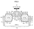
- Figure 3 shows the construction of a p-channel MOS transistor 10 according to a first embodiment of the present invention.
- the p-channel MOS transistor 10 is formed on an n-type device region 11A defined on a silicon substrates of a (001) surface orientation by a STI device isolation region 11I, wherein a high quality gate insulation film 12 of a thermal oxide film or an SiON film is formed on the silicon substrate 11 in correspondence to a channel region in the device region 11A with a thickness of about 1.2nm.
- each CVD oxide film 12I extends continuously and covers the sidewall surface of the gate electrode 13. Further, sidewall insulation films 13A and 13B are formed on the respective sidewall surfaces of the gate electrode 13 via the respective thermal oxide films 12I.
- trenches 11TA and 11TB are formed in the silicon substrate 11 at respective outer sides of the sidewall insulation films 13A and 13B, wherein the foregoing trenches 11TA and 11TB are filled with respective p-type SiGe mixed crystal regions 14A and 14B, which are grown epitaxially on the silicon substrate 11 at the foregoing trenches 11TA and 11TB.
- the SiGe regions 14A and 14B thus grown epitaxially to the silicon substrate 11 have a larger lattice constant as compared with the Si crystal that constitutes the silicon substrate 11, the SiGe regions 14A and 14B induces a uniaxial compressive stress in the channel region formed in the silicon substrate 11 right underneath the gate electrode 13 by the mechanism explained previously with reference to Figure 1.
- n-type pocket injection regions 11p in the silicon substrate 11 in correspondence to the device region 11A by injecting an n-type impurity element such as Sb obliquely to the regions of the silicon substrate 11 at both lateral sides of the gate electrode 13. Further, a source extension region 11a and a drain extension region 11b of p-type are formed so as to partially overlap with the foregoing pocket injection regions 11p.
- the foregoing p-type source and drain extension regions 11a and 11b extend up to the p-type SiGe mixed crystal regions 14A and 14B respectively, wherein it should be noted that the p-type SiGe mixed crystal regions 14A and 14B are formed in continuation with the p-type diffusion regions 11S and 11D respectively. It should be noted that the p-type diffusion regions 11S and 11D constitute respectively the source region and the drain regions of the p-channel MOS transistor 10.
- the p-type diffusion regions 11S and 11D are formed so as to include the SiGe mixed crystal regions 14A and 14B respectively.
- direct contact between the p-type SiGe mixed crystal region 14A or 14B having a small bandgap and the n-type Si well that constitutes the device region 11A is eliminated, and occurrence of leakage current at the pn junction of Si/SiGe interface is suppressed.
- Si epitaxial layers 15A and 15B are formed on the SiGe mixed crystal regions 14A and 14B respectively, and silicide layers 16A and 16B are formed on the surface of the Si epitaxial layers 15A and 15B. Further, a similar silicide layer 16C is formed on the gate electrode 13.
- each of the SiGe mixed crystal regions 14A and 14B is defined by sidewall surfaces 14a, 14b, 14c and also a bottom surface 14d as shown in Figure 3, wherein it should be noted that each of the sidewall surfaces 14a, 14b, 14c and the bottom surface 14d is formed of a flat facet.
- the bottom surface 14d is formed of a (001) surface parallel to the principal surface of the silicon substrate 11 while the facet 14b forms an angle ⁇ 2 generally perpendicular to the bottom surface 14d. Further, the facet 14c forms a smaller angle ⁇ 1 than the foregoing angle ⁇ 2 with respect to the bottom surface 14d.
- the mutually opposing sidewall surfaces of the SiGe mixed crystal regions 14A and 14B that define the channel region right underneath the gate insulation film 12 are formed of the facet 14b that extends perpendicularly to the principal surface of the silicon substrate 11.
- the distance between the mutually opposing SiGe mixed crystal regions 14A and 14B does not increase in the downward direction of the silicon substrate 11 from the interface between gate insulation film 12 and the silicon substrate 11, contrary to the conventional construction of Figure 1 or Figure 2, and it becomes possible to confine the uniaxial compressive stress to the channel region effectively.
- the facet 14c is formed such that the SiGe mixed crystal regions 14A and 14B do not protrude to the n-type well constituting the device region in the silicon substrate 11 from the p-type diffusion region that constitutes the source region 14S or the drain region 14D.
- the sidewall surface defining the SiGe mixed crystal region 14A or 14B changes the angle thereof to the principal surface of the silicon substrate 11 discontinuously from the angle ⁇ 2 to the angle ⁇ 1 at the part where the facet 14b meets the facet 14c, while such a discontinuous change of the facet angle enables concentration of the compressive stress to the part of the device region 11A located between the SiGe mixed crystal regions 14A and 14B.
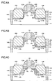
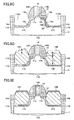
- Figures 4A - 4F show various modifications of the p-channel semiconductor device according to the first embodiment of the present invention.
- those parts corresponding to the parts explained previously are designated by the same reference numerals and description thereof will be omitted.
- Figures 4A - 4F show the state before formation of the silicide regions 16A - 16C.
- illustration of the pocket injection regions 11p will be omitted.
- the sidewall surfaces of the SiGe mixed crystal regions 14A and 14B are formed by the facet 14b generally perpendicular to the principal surface of silicon substrate 11 and also by the bottom surface 14d parallel to the principal surface of the silicon substrate 11, wherein the facet 14b and the bottom surface 14d form an angles of substantially 90 degrees.
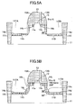
- the trenches 11TA and 11TB are formed by a dry etching process as shown in Figure 5A, wherein the location of the bottom surface 14d of the SiGe mixed crystal regions 14A and 14B are set such that the corner part of the SiGe mixed crystal regions 14A and 14B, where the facet 14b and the bottom surface 14d intersect with each other, does not protrude into the region of the n-type well from the foregoing source/drain regions 11S and 11D. Filling of the trenches 11TA and 11TB with the SiGe mixed crystal regions 14A and 14B will be described in detail later.
- Figure 4B corresponds to the construction of Figure 3 explained previously, in which the facet 14b is formed perpendicularly to the silicon substrate 11 at first by forming the trenches 11TA and 11TB by a dry etching process, as shown in Figure 5B, wherein the facet 14c under the facet 14b is formed subsequently by applying a thermal processing to the silicon substrate 11 at 550°C in a hydrogen ambient after the foregoing dry etching process.
- the facet 14c is formed by the Si (111) surface that forms an angle of 56 degrees with respect to the principal surface of the silicon substrate 11.
- the construction of Figure 4C is formed by forming the trenches 11TA and 11TB by applying a wet etching process to the silicon substrate 11 by using an organic alkaline etchant (hydration tetramethyl ammonium: TMAH, choline, or the like) or hydration ammonium, or alternatively, by applying a heat treatment of 800°C in an ambient of hydrogen gas and HCl as shown in Figure 5C.
- TMAH tetramethyl ammonium
- the facet 14b perpendicular to the silicon substrate 11 is not formed in the SiGe mixed crystal layer regions 14A and 14B, and instead, a facet 14c of a Si (111) surface starts right away from the interface between the gate insulation film 12 and the silicon substrate 11 with the angles of 56 degrees to the principal surface of the silicon substrate 11.
- the facet 14b is formed at first in the silicon substrate 11 perpendicularly to the principal surface of the silicon substrate 11, while the facet 14b is changed to a slope formed of the (111) surface by applying a wet etching process to the facet 14b by using TMAH. Further, there is formed another facet 14c formed of the (111) surface.
- the facet 14b and the facet 14c thus formed define together a space of wedge form as the foregoing trenches 11TA and 11TB, such that the wedge formed trenches 11TA and 11TB invade in the silicon substrate 11 into the region right underneath the sidewall insulation films 13A and 13B toward the channel region.
- the facet 14c forms the angle of about 56 degrees to the principal surface of the silicon substrate 11 in correspondence to the Si (111) surface, while the facet 14b forms the angle of about 146 degrees also in correspondence to the Si (111) surface.
- the SiGe mixed crystal regions 14A and 14B grown so as to fill the wedge-shaped trenches 11TA and 11TB have respective tip ends invading to the region right underneath the sidewall insulation films 13A and 13B and coming close to the channel region formed right underneath the gate insulation film 12.
- a strong uniaxial compressive stress is applied to the channel region and mobility of the holes is improved significantly in the channel region.
- concentration of stress at such a tip end part there occurs concentration of stress at such a tip end part, and the effect of increasing the stress in the channel region is enhanced further.
- Figure 4E is the one based on the construction of Figure 4D and represents the case in which formation of the Si epitaxial layers 15A and 15B on the SiGe mixed crystal regions 14A and 14B is omitted.
- Figure 4F is also based on the construction of Figure 4D and represents the case in which a channel layer 11G of a SiGe mixed crystal is formed epitaxially on the silicon substrate 11 in correspondence to the region right underneath the gate insulation film 12. According to such a construction, the channel layer 11G itself induces the uniaxial compressive stress, and it becomes possible to improve the mobility of the holes further in the channel layer 11G.
- Figure 6 is a diagram summarizing the formation process of trenches 11TA and 11TB shown in Figures 5A - 5D in which the epitaxial growth of the SiGe mixed crystal regions 14A and 14B is made.
- the silicon substrate 11 is a so-called (001) substrate having a (001) surface
- the trenches 11TA and 11TB have respective sidewall surfaces each defined by a bottom surface 14d and facets 14b and 14c.
- the facet 14b forms the angle ⁇ 2 to the principal surface of silicon substrate 11, while the facet 14c forms the angle ⁇ 1 with respect to the principal surface of the silicon substrate 11.
- the bottom surface 14d is formed at the depth y1 as measured from the interface between the gate insulation film 12 and the silicon substrate 11, while the facet 14b is formed down to the depth y2.
- the gate electrode 13 extends on the surface of the silicon substrate 11 generally in the ⁇ 110> direction
- the gate electrode 13 may extend also generally in the ⁇ 100> direction.
- any of the foregoing angles ⁇ 1 and ⁇ 2 to about 90 degree and the depth y1 to 20 - 70nm. It should be noted that such a depth y1 can be controlled with high precision by using a dry etching process.
- the angle ⁇ 1 takes the value of 56 degrees in the case the facet 14c is formed of the Si (111) surface as explained before with reference to Figure 4B.
- the foregoing angle ⁇ 1 is by no means limited to the angles of 56 degrees.
- the angle ⁇ 2 can be controlled with high precision by the heat treatment process conducted subsequently to the foregoing dry etching process at about 550°C in the hydrogen ambient.
- the angles ⁇ 1 and ⁇ 2 take the range of 50 - 60 degrees, and in the special case in which the facet 14c is formed of the Si (111) surface, the angles ⁇ 1 and ⁇ 2 take the value of 56 degrees.
- the angles ⁇ 1 and ⁇ 2 are by no means limited to the foregoing angle of 56 degrees.
- the depth y2 becomes zero in the construction of Figure 4C, it is preferable to set the depth y1 to the range of 20 - 70nm.
- angle ⁇ 1, ⁇ 2 and the depth y1 can be controlled with high precision by using a wet etching process applied to the silicon substrate 11 while using the organic alkaline etchant such as TMAH, or alternatively, by a high temperature gas phase etching process conducted in a HCl/hydrogen ambient.
- angles ⁇ 1 and ⁇ 2 and also the depths y1 and y2 precisely, by combining the dry etching process and the wet etching process at the time of formation of the trenches 11TA and 11TB.
- the angles ⁇ 1 and ⁇ 2 take the value of 56 degrees and 146 degrees respectively in the case the facets 14b and 14c are formed by the Si (111) surface.
- the construction of Figures 4D - 4F is not limited in the case in which the facets 14b and 14c are formed by the Si (111) surface.
- the p-type source region 11S and the p-type drain region 11D are formed in the silicon substrate 11 at the outer sides of the sidewall insulation films 13A and 13B, prior to the formation of the trenches 11TA and 11TB. It should be noted that the trenches 11TA and 11TB are formed inside such p-type diffusion regions so as not to exceed the p/n junction interface thereof.
- any of the methods of Figures 5A - 5D it is possible to form the trenches 11TA and 11TB directly in the n-type Si well formed in the device region 11A of the silicon substrate 11 before formation of the source/drain diffusion region 11S, 11D as shown in the example of Figure 7 and thereafter grow a p-type Si layer selectively on the surface of the trenches 11TA and 11TB while supplying the Si gaseous source together with a p-type dopant gas.
- the device region 11A is defined on the surface of p-type silicon substrate 11 by the STI type device isolation structure 11I, and an n-type well is formed in the device region 11A by injecting an n-type impurity element into the device region 11A.
- the gate insulation film 12 and the polysilicon gate electrode 13 are formed on the silicon substrate 11 in correspondence to the device region 11A as a result of patterning of an SiON film and a polysilicon film formed uniformly on the silicon substrate 11, and the p-type source extension region 11a and the p-type drain extension region 11b are formed in the device region 11A by injection of a p-type impurity element such as B+ while using the polysilicon gate electrode 13 as a mask.
- the p-type impurity element such as B+ is injected once more, and as a result, the p-type source region 11S and the p-type drain region 11D are formed in the device region 11A of the silicon substrate 11 at the outer sides of the sidewall insulation films 13A and 13B.
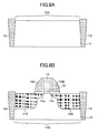
- a part of the device region of the silicon substrate 11 outside the sidewall insulation films 13A and 13B are etched first by a dry etching process with the depth of 10 - 60nm.
- each trench is defined by vertical sidewall surfaces perpendicular to the principal surface of the silicon substrate 11 and a horizontal bottom surface, similarly to the case of Figure 5A explained previously.
- the vertical sidewall surface is etched further by a wet etching process that uses TMAH as the etchant, and with this, the trenches 11TA and 11TB are formed such that the facets 14b and 14c define the wedge-shaped sidewall surface of the trenches 11TA and 11TB.
- TMAH TMAH
- the structure of Figure 8C is introduced into a low-pressure CVD apparatus filled with an inert gas such as hydrogen gas, nitrogen gas, Ar gas, He gas, or the like, and held to the pressure of 5 - 1330Pa, after a removal process of native oxide film, and held for 5 minutes in the maximum at the foregoing pressure of 5 - 1330Pa (H 2 -Bake) after heating to the temperature of 400 - 550°C in a hydrogen ambient (Heat-UP).
- an inert gas such as hydrogen gas, nitrogen gas, Ar gas, He gas, or the like
- a silane (SiH 4 ) gas, a germane (GeH 4 ) gas and a diborane (B 2 H 6 ) gas are supplied over the duration of 1 - 40 minutes respectively as the gaseous source of Si, the gaseous source of Ge and the dopant gas, with respective partial pressures of 1 - 10Pa, 0.1 - 10Pa and 1 ⁇ 10 -5 - 1 ⁇ 10 -3 Pa, in addition to a hydrogen chloride (HCl) gas supplied as an etching gas with the partial pressure of 1 - 10Pa.
- HCl hydrogen chloride
- the crystal quality of the SiGe mixed crystal layers 14A and 14B is improved particularly when the (100) surface or (111) surface of Si is exposed at the bottom surface or sidewall surface of the trenches 11TA and 11TB.
- the construction having the sidewall surface of the wedge form defined by the facets 14b and 14c forming the Si (111) surfaces shown in Figure 8C is thought advantageous for the trenches 11TA and 11TB.
- the SiGe mixed crystal layers 14A and 14B filling the trenches 11TA and 11TB induce the uniaxial compressive stress originating from the lattice constant difference with respect to the silicon substrate 11 in the channel region right underneath the gate insulation film 12 in the foregoing device region 11A. Because the tip end parts of the wedges invade to the regions located right underneath the sidewall insulation films 13A and 13B in the silicon substrate 11, a large compressive stress is applied to the channel region right underneath the gate insulation film 12.
- a p-type semiconductor layer primarily formed of Si is formed on the SiGe mixed crystal layers 14A and 14B to a thickness Ys of 0 - 20nm, by supplying the silane gas and the diborane gas with respective partial pressures of 1 - 10Pa and 1 ⁇ 10 -4 -1 ⁇ 10 -2 Pa, together with the hydrogen chloride (HCl) gas of the partial pressure of 1 - 10Pa, at the temperature equal to or lower than the temperature used for forming the SiGe mixed crystal layers 14A and 14B.
- the cap layers 15A and 15B are respectively formed on the SiGe mixed crystal regions 14A and 14B (CapSi-Depo).
- the thickness Ys is set to 0nm means that there occurs no formation of the cap layers 15A and 15B.
- cap layers 15A and 15B are provided in anticipation of the silicide formation process of Figure 8E, and thus, it is preferable to use a p-type silicon layer, on which silicide formation is made easily, while it is possible that the cap layers 15A and 15B contain Ge with the atomic concentration if 0 - 20%. Further, it is possible to use a SiGeC mixed crystal layer containing about 2% of C (carbon) in terms of atomic concentration for the cap layers 15A and 15B. In the case Ge is to be incorporated into the cap layers 15A and 15B, a GeH 4 gas may be added to the gaseous source in the growth process of the cap layers with a partial pressure of 0 - 0.4Pa.
- the material constituting the sidewall insulation films 13A and 13B contains Si with relatively large amount, the selectivity of growth of the SiGe mixed crystal layer tends to become deteriorated, and there may be caused a growth of SiGe nuclei on such sidewall insulation films 13A and 13B in the case the growth of SiGe mixed crystal regions have been conducted according to the foregoing process.
- the structure of Figure 8D is exposed to a hydrogen chloride (HCl) gas for short time period at the same temperature used for growing the SiGe mixed crystal regions 14A and 14B or lower, such that the part of the sidewall insulation films 13A and 13B or the device isolation structure 11I that may become the nuclei of silicide growth is removed by etching (PostEtch).
- HCl hydrogen chloride
- the structure thus obtained is then cooled to the temperature below 400°C in an inert ambient (CoolDown) and taken out from the low pressure CVD apparatus.
- this PostEtch process can be conducted for example in an inert or reducing ambient of hydrogen, nitrogen, He, or the like, under the process pressure of 5 - 1000Pa while supplying the hydrogen chloride gas with the partial pressure of 10 - 500Pa over the duration of typically 0 - 60 minutes.
- the substrate of Figure 8D thus taken out is introduced to a sputtering apparatus in the process of Figure 8E and silicide films 16A and 16B of nickel silicide or cobalt silicide are formed on the cap layers 15A and 15B respectively, by a salicide process.
- a silicide film 16C is formed also on the polysilicon gate electrode 13 simultaneously.
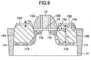
- the SiGe mixed crystal layers 14A and 14B have the thickness Y2 of 20 - 70nm corresponding to the depth of the trenches 11TA and 11TB in the part located under the interface between the gate insulation film 12 and the silicon substrate 11, the epitaxial growth of the SiGe mixed crystal layers 14A and 14B is continued to the height Y1 of 0 - 30nm beyond the foregoing interface.
- the height Y1 is 0nm, this means that the SiGe mixed crystal layers 14A and 14B are not grown beyond the interface between the gate insulation film 12 and the silicon substrate 11.
- silicide layers 16A and 16B it is preferable to control the salicide process for forming the silicide layers 16A and 16B such that the silicide layers 16A and 16B do not to reach the SiGe mixed crystal regions 14A and 14B across the cap layers 15A and 15B.
- the part of the SiGe mixed crystal regions 14A and 14B grown beyond the interface of the gate insulation film 12 and the silicon substrate 11 has a side surface defined by the facet 14a at the side facing the channel region, while the side facing the device isolation structure 11I is defined by the facet 14e.
- the facet 14a forms an angle ⁇ 3 of 40 - 90 degree and the facet 14b forms an angle ⁇ 4 of 40 - 60 degree.
- the silicide layers 16A and 16B on the cap layers 15A and 15B are not formed in contact with the sidewall insulation film 13A or 13B of the gate electrode 13, and it becomes possible to suppress the problems of occurrence short circuit through the silicide layers 16A and 16B or formation of parasitic capacitance between and gate electrode 13 and the silicide layer 16A or 16B.
- this "effective" critical thickness increases with decreasing growth temperature, and thus, it becomes possible to induce the distortion in the channel region of the MOS transistor more effectively, by using the SiGe mixed crystal grown selectively in a localized area at a low temperature.
- the epitaxial growth of the SiGe mixed crystal layers 14A and 14B is possible up to the atomic concentration level of Ge of about 40%.
- the dopant concentration in the SiGe mixed crystal regions 14A and 14B is set to the range of 1 ⁇ 10 18 - 1 ⁇ 10 21 cm -3 .
- the dopant concentration of B is set to about 1 ⁇ 10 18 - 1 ⁇ 10 20 cm -3 in the cap layers 15A and 15B characterized by low Ge concentration level.
- Figure 10A is a diagram summarizing the process of Figure 8D conducted in a low-pressure CVD apparatus explained above as a third embodiment the present invention.
- a substrate to be processed is introduced into the low-pressure CVD apparatus at the temperature of 400°C or lower at first, and the temperature is raised to a predetermined process temperature of 400 - 550°C in a hydrogen ambient (HeatUp).
- the substrate to be processed is held at the same process temperature in the same hydrogen ambient for the duration of 5 minutes in the maximum, and a hydrogen heat treatment process is conducted (H 2 -Bake).
- the processing gas introduced to the low-pressure CVD apparatus is changed at the same process temperature, and the epitaxial growth of the p-type SiGe mixed crystal regions 14A and 14B is conducted in the trenches 11TA and 11TB as explained previously (SiGe Depo).
- the composition or partial pressure of the processing gas introduced into the low-pressure CVD apparatus is changed subsequently to the epitaxial growth of the p-type SiGe mixed crystal regions 14A and 14B while maintaining the same process temperature of 400 - 550°C, and the cap layers 15A and 15B of p-type Si or p-type SiGe(C) mixed crystal are grown epitaxially on the SiGe mixed crystal regions 14A and 14B (Cap Si Depo).
- a hydrogen chloride gas is introduced, after formation of the cap layers 15A and 15B, into the low-pressure CVD apparatus in the inert or hydrogen ambient at the process temperature of 400 - 550°C.
- any structure that can become the nuclei of silicide formation in the silicide formation process of Figure 8E is removed from the sidewall insulation film 13A, 13B or the device isolation structure 11I (Post Etch), and the substrate temperature is subsequently lowered to 400°C or lower (Cool Down) in the hydrogen or inert gas ambient.
- Figure 10B shows the process corresponding to the embodiment explained previously with reference to Figure 9 in which the source region 11S and the drain region 11D are formed growing a p-type Si layer epitaxially after formation of the trenches 11TA and 11TB so as to cover the sidewall surface thereof.
- the source region 11S and the drain region 11D can be formed in this case by introducing the silane gas and the diborane gas and the HCl gas into the low-pressure CVD apparatus with respective partial pressures of 1 - 10Pa, 1 ⁇ 10 -4 - 1 ⁇ 10 -2 Pa and 1 - 10Pa, for example, after the foregoing H 2 -Baking process, at the specified process temperature of 400 - 550°C.
- Figure 11 is a diagram showing the construction of the low-pressure CVD apparatus 40 used for the process of Figure 8D or the process of Figures 10A - 10C explained before.
- the low-pressure CVD apparatus 40 is a so-called cluster type substrate processing apparatus in which the CVD reaction furnace 41 for conducting the process steps of Figures 10A - 10C are connected to a preprocessing chamber 43 via a substrate transportation chamber 42 filled with an inert gas such as a nitrogen gas, and the substrate W having the structure corresponding to the state of Figure 10C is introduced into the substrate transportation chamber 42 via a gate valve not illustrated, wherein the substrate thus introduced is transported from the substrate transportation chamber 42 to the preprocessing chamber 43.
- an inert gas such as a nitrogen gas
- a preprocessing for removing the native oxide film from the substrate surface is conducted by conducting a processing in a diluted hydrofluoric acid (DHF) and subsequent water rinse processing, or by a hydrogen radical cleaning processing, or alternatively by an HF gas phase processing.
- DHF diluted hydrofluoric acid
- the substrate finished with the preprocessing process is transported to the CVD reaction furnace 41 through the substrate transportation chamber 42 without being exposed to the air and the process steps of Figures 10A - 10C are conducted.
- a thermal oxide film or an SiON film having a larger specific dielectric constant than a thermal oxide film is used frequently for the gate insulation film 12.
- Figure 12A is a plan view showing the part of the silicon substrate 11 including the device isolation region 11I and the device region 11A
- Figure 12B is a cross-sectional view of Figure 12A taken in the gate width direction
- Figure 12C shows the structure of Figure 12B in the state in which the trenches 11TA and 11TB are formed in the device region 11A and the trenches 11TA and 11TB thus formed are filled with the p-type SiGe mixed crystal regions 14A and 14B.
- the SiGe mixed crystal regions are formed on the undulating bottom surface with a flat top surface.
- increase and decrease of volume of the SiGe mixed crystal caused by undulation of the bottom surface is cancelled out at the level shown in Figure 12C by the dotted line, and compressive stress similar to the one obtained for the case in which the SiGe mixed crystal regions are formed on a flat surface is obtained in the channel region.
- the gate width GW is small, there appears only a convex surface on the surface of the device region 11A as it shown in Figures 13A and 13B, and thus, the effective volume of the SiGe mixed crystal regions 14A and 14B is decreased by the effect of the convex surface at the bottom surface in the case the trenches 11TA and 11TB are formed on the silicon substrate surface having such a convex surface and the trenches are filled with the SiGe mixed crystal regions 14A and 14B, in view of the flat surface of the SiGe mixed crystal regions 14A and 14B appearing as a result of the self-limiting effect. Thereby, the compression stress induced in the channel region is decreased substantially.
- the present embodiment carries out the removal process of the native oxide, conducted immediately before formation of the gate insulation film 12 for removing the native oxide film from the silicon substrate surface, in an ambient not containing hydrogen, such as the ambient of nitrogen, Ar or He, for example, at the temperature that does not exceed 900°C.
- an ambient not containing hydrogen such as the ambient of nitrogen, Ar or He, for example, at the temperature that does not exceed 900°C.
- a mask M is formed on a polysilicon film 13M used for forming the polysilicon gate electrode 13 in correspondence to the polysilicon gate electrode 13 at the time of forming the polysilicon gate electrode 13, by using a silicon oxide film or silicon nitride film as shown in Figure 14A.
- the structure of Figure 14A is exposed to a hydrogen/diborane gas mixture ambient at the temperature of 300 - 550°C, to form a B (boron) film 13Bo on the polysilicon film 13M in correspondence to the region where the gate electrode 13 is formed with the thickness of 1 - 10nm.
- the polysilicon film 13M is pattered to form the gate electrode 13 and the sidewall insulation films 13A and 13B are formed.
- representation of the CVD oxide film 12I is omitted.
- the boron mask pattern 13Bo is formed on the top part of the polysilicon gate electrode 13.
Landscapes
- Insulated Gate Type Field-Effect Transistor (AREA)
- Chemical & Material Sciences (AREA)
- Crystallography & Structural Chemistry (AREA)
- Thin Film Transistor (AREA)
Abstract
Description
- The present application is based on Japanese priority application No.2004-380619 filed on December 28, 2004, the entire contents of which are hereby incorporated by reference.
- The present invention generally relates to semiconductor devices and more particularly to a semiconductor device having improved operational speed as a result of stressing and the fabrication process thereof.
- With progress in the art of device miniaturization, it is now possible to fabricate ultrafine and ultra high-speed semiconductor devices having a gate length of 100nm or less.
- In such ultrafine and ultra high-speed transistors, the area of the channel region right underneath the gate electrode is reduced as compared with conventional semiconductor devices, and the mobility of electrons or holes traveling through the channel region is influenced heavily by the stress applied to such a channel region.
- Thus, there are various attempts made for improving the operational speed of the semiconductor device by optimizing the stress applied to such a channel region.
- In semiconductor devices that use a silicon substrate as a channel region, the mobility of holes is generally smaller than the mobility of electrons, and thus, it is particularly important to improve the operational speed of p-channel MOS transistors, in which holes are used for the carriers, in the designing of semiconductor integrated circuits.
- With such p-channel MOS transistors, it is known that the mobility of carriers is improved by applying a uniaxial compressive stress to the channel region, and there is a proposal to use the construction of Figure 1 as the means of applying the compressive stress to the channel region.
- Referring to Figure 1, there is formed a
gate electrode 3 on asilicon substrate 1 via agate insulation film 2, and p-type diffusion regions silicon substrate 1 at both lateral sides of thegate electrode 3 so as to define the channel region. Further,sidewall insulation films gate electrode 3 so as to cover also a surface part of thesilicon substrate 1. - Thereby, the
diffusion regions gate electrode 3 from thediffusion region 1a to thediffusion region 1b is controlled by the gate voltage applied to thegate electrode 3. - Further, there are formed SiGe mixed
crystal regions silicon substrate 1 in the construction of Figure 1 at respective outer sides of thesidewall insulation films silicon substrate 1, and p-type source and drain regions are formed in the SiGe mixedcrystal regions diffusion region 1a and thediffusion region 1b. - Because the SiGe mixed
crystal regions silicon substrate 1 in the MOS transistor of the construction of Figure 1, the SiGe mixedcrystal regions crystal regions silicon substrate 1 as shown by an arrow b. - Because the SiGe mixed
crystal regions silicon substrate 1, such a deformation of the SiGe mixedcrystal regions - As a result of such a uniaxial compressive stress applied to the channel region of the MOS transistor of Figure 1, the symmetry of the Si crystal constituting the channel region is locally modulated, and as a result of such local modulation of the symmetry, degeneration of heavy holes and light holes in the valence band is resolved. Thereby, there is caused increase of hole mobility in the channel region, leading to improvement of operational speed of the transistor.
- It should be noted that such increase of hole mobility caused in the channel region by locally induced stress appears particularly conspicuously in the ultrafine semiconductor devices having a gate length of 100nm or less.
-
- (Patent Reference 1) Unites States Patent 6,621,131
- (Patent Reference 2) Japanese Laid-Open Patent Application 2004-31753
- (Non-Patent Reference 1) Thompson, S. E., et al., IEEE Transactions on Electron Devices, vol.51, No.11, November, 2004, pp.1790 - 1797
- Figure 2 shows the construction of a p-channel MOS transistor based on such a principle and described in Non-Patent
Reference 1. In the drawing, those parts corresponding to the parts described previously are designated by the same reference numerals and the description thereof will be omitted. - Referring to Figure 2, the SiGe mixed
crystal regions silicon substrate 1 up to the level higher than the interface between thesilicon substrate 1 and thegate electrode 2 represented in the drawing by a dotted line L, - Further, it should be noted that the mutually facing side surfaces 1As and 1Bs of the SiGe mixed
crystal regions crystal regions silicon substrate 1 from the lower surface of thegate insulation film 2. - Further, in the conventional construction of Figure 2 in which the SiGe mixed
crystal regions silicide layer 4. Asimilar silicide layer 4 is formed also on thepolysilicon gate electrode 3. - Further, in
Non-Patent Reference 1 corresponding to the MOS transistor of Figure 2, the use of a SiGe mixed crystal having the composition of Si0.83Ge0.17 is disclosed for the SiGe mixedcrystal regions foregoing Non-Patent Reference 1 discloses the Ge concentration of 15 atomic percent for the SiGe mixedcrystal regions - On the other hand, it is thought that the operational speed of the p-channel MOS transistor would be increased further when the uniaxial compressive stress in the channel region is increased further in such a conventional p-channel MOS transistor.
- Further, it is noted that, in the conventional art of
Patent Reference 1, the epitaxial regrowth process the SiGe mixedcrystal regions diffusion regions - Further, it is noted that the conventional p-channel MOS transistor of Figure 2 forms the
silicide film 4 directly on the epitaxially grown SiGe mixedcrystal regions crystal regions - Further, such formation of silicide layer on the SiGe mixed crystal layer causes various problems such as degradation of heat resistance or morphology of the silicide with increasing Ge concentration in the SiGe mixed crystal layer, and it becomes difficult to form such a silicide layer on the SiGe mixed crystal layers with ordinary salicide process in the case the SiGe mixed crystal contains high concentration Ge for increasing the stress as in the case of the p-channel MOS transistor of Figure 2.
- In a first aspect, the present invention provides a semiconductor device, comprising:
- a silicon substrate including a channel region;
- a gate electrode formed on said silicon substrate in correspondence to said channel region via a gate insulation film, said gate electrode carrying respective sidewall insulation films on a pair of mutually opposing sidewall surfaces thereof;
- source and drain extension regions formed in said silicon substrate at respective lateral sides of said gate electrode across said channel region in the form of a p-type diffusion region;
- source and drain regions formed in said silicon substrate at respective outer sides of said sidewall insulation films in the form of a p-type diffusion region respectively as a continuation of said source extension region and a continuation of said drain extension region; and
- a pair of SiGe mixed crystal regions formed in said silicon substrate at respective outer sides of said sidewall insulation films so as to be included in said source region and said drain region, respectively, said pair of SiGe mixed crystal regions having an epitaxial relationship with said silicon substrate,
- each of said SiGe mixed crystal regions being grown to a level higher than an interface between said gate insulation film and said silicon substrate,
- each of said SiGe mixed crystal regions having a sidewall surface facing to another SiGe mixed crystal region such that said sidewall surface is defined by a plurality of facets forming respective, different angles with respect to a principal surface of said silicon substrate.
- In another aspect, the present invention provides a method of fabricating a semiconductor device having a pair of SiGe compressive stressors at respective lateral sides of a channel region, comprising the steps of:
- forming a gate electrode on said silicon substrate in correspondence to said channel region via a gate insulation film;
- forming a pair of p-type diffusion regions in said silicon substrate in correspondence to respective lateral sides of said gate electrodes;
- forming a pair of p-type diffusion regions in said silicon substrate in correspondence to respective lateral sides of said gate electrode with a separation from said channel region by a distance corresponding to a thickness of respective gate sidewall insulation films on said gate electrode as source and drain regions;
- forming a pair of trenches in said silicon substrate respectively in correspondence to source and drain regions by conducting an etching process, such that each of said trenches has a sidewall surface defined by a plurality of facets and such that, in each of said trenches, said sidewall surface and a bottom surface are covered continuously by said p-type diffusion region constituting said source or said drain region; and
- filling said trenches by an epitaxial growth of a p-type SiGe layer,
- said epitaxial growth of said p-type SiGe layer is conducted at a temperature of 400 - 550°C.
- In another aspect, the present invention provides a method of fabricating a semiconductor device having a pair of SiGe compressive stressors at both lateral ends of a channel region, comprising the steps of:
- forming a gate electrode on a silicon substrate in correspondence to said channel region via a gate insulation film;
- forming a pair of p-type diffusion regions in said silicon substrate in correspondence to both lateral sides of said gate electrode;
- forming a pair of trenches in said silicon substrate respectively in correspondence to lateral sides of said gate electrode with a separation from said channel region corresponding to a gate sidewall insulation film formed on said gate electrode, such that each of said trenches has a sidewall surface defined by a plurality to f facets;
- covering, in each of said pair of trenches, said sidewall surface and a bottom surface of said trench by a Si epitaxial layer doped to p-type; and
- filling, in each of said trenches, said trench by growing a p-type SiGe mixed crystal layer epitaxially on said Si epitaxial layer,
- said step of growing said p-type SiGe layer epitaxially being conducted at a temperature of 400 - 550°C.
- According to the present invention, a uniaxial compressive stress is applied to the channel region by growing a p-type SiGe mixed crystal layer at both lateral sides of said channel region epitaxially, and the mobility of holes transported through the channel region is improved significantly.
- Thereby, the present invention achieves optimization of the uniaxial stress applied to the channel region by forming the foregoing pair of p-type SiGe mixed crystal regions such that respective, mutually facing sidewall surfaces are formed of plurality of facets forming respective, different angles with respect to a principal surface of said silicon substrate, and the operational speed of the semiconductor device is improved further as compared with the conventional construction in which the foregoing sidewall surfaces of the SiGe mixed crystal regions are defined by a continuous, curved surface and thus the distance between the SiGe mixed crystal regions across the channel region increases rapidly with increasing distance in the downward direction of the silicon substrate from the interface between the gate insulation film and the silicon substrate.
- Particularly, by forming the sidewall surfaces of the SiGe mixed crystal regions to have a wedge shape such that the respective SiGe mixed crystal regions invade to the region right underneath the gate sidewall insulation films from both lateral sides of the channel region, it becomes possible with the present invention to maximize the uniaxial compressive stress applied to the silicon substrate in such a channel region, including the effect of stress concentration at the wedge tip end part.
- Further, because each of the p-type SiGe mixed crystal regions are formed on a limited area of the silicon substrate, it has been discovered that it is possible to increase the Ge concentration in the p-type SiGe mixed crystal regions beyond the limiting concentration corresponding to the critical thickness up to the concentration of 40% in terms of atomic percent, contrary to the case of forming a continuous, two-dimensional film. Thereby, the effect of improvement of the semiconductor device caused by the compressive stress can be maximized.
- In the present invention, on the other hand, it is preferable to suppress the Ge atomic concentration such that the Ge atomic concentration does not exceed 28% in view of avoiding the problem of degradation of crystal quality of the foregoing p-type SiGe mixed crystal regions, which starts, according to the discovery of the inventor of the present invention, when the Ge atomic concentration has exceeded the value of 28%.
- Further, according to the present invention, it becomes possible to reduce the adversary effect of the tensile stress caused by the silicide layers formed on the source/drain regions of the semiconductor device, by growing the p-type SiGe mixed crystal regions beyond the level of the interface between the gate insulation film of the semiconductor device and the silicon substrate. It should be noted that such a tensile stress cancels out the effect of the uniaxial compressive stress induced in the channel region.
- Particularly, by growing a p-type Si layer or a p-type SiGe layer of small Ge concentration on the foregoing p-type SiGe mixed crystal regions epitaxially, it becomes possible to avoid the problems associated with the difficulty of forming a silicide layer on a SiGe mixed crystal layer of high Ge concentration.
- It should be noted that the increase of hole mobility caused by application of compressive stress to the channel region of the p-channel MOS transistor appears most conspicuously when the silicon substrate is a so-called (001) substrate and the gate electrode is formed on the silicon substrate in the <110> direction.
- Further, according to the present invention, in which the trench is formed at both lateral sides of the gate electrode after forming the p-type diffusion regions and such trenches are filled with the p-type SiGe mixed crystal layer by a low temperature process that uses the deposition temperature of 400 - 550°C, the impurity distribution profile of the diffusion regions formed already is not modified, and it becomes possible to construct the semiconductor device with the desired characteristics. Further, as a result of such a low temperature growth, it becomes possible to introduce Ge into the p-type SiGe mixed crystal layer with the concentration reaching 40% in terms of atomic percent.
- Further, according to the present invention, it becomes possible to form a silicide layer in electrical connection with the source/drain regions of the semiconductor device by forming a Si epitaxial cap layer substantially free from Ge or having a Ge concentration of 20% or less, on the SiGe mixed crystal layer grown by the low temperature epitaxial process. Further, with such a construction in which the silicide layer is formed on the cap layer at the level far above the interface between the gate insulation film and the silicon substrate, the problem of cancellation of the uniaxial compressive stress caused in the channel region by the tensile stress caused by the silicide layer is reduced.
- Further, with the formation of such a cap layer of relatively low Ge concentration, it becomes possible to suppress the degradation of heat resistance of the silicide layer or degradation of surface morphology of the silicide layer, which occur when the Ge concentration is increased, and stable and reliable formation of silicide becomes possible.
- With the present invention, it is also possible to form the trenches in the silicon substrate at first. In this case, the SiGe mixed crystal layer is grown after growing the p-type Si epitaxial layer on the surface of the trenches. According to such a process, too, the problem of modification of the impurity distribution profile in the source extension region and drain extension region formed by injecting the impurity elements while using the gate electrode is effectively avoided.
- Meanwhile, in such ultrafine and ultra fast semiconductor devices that apply the compressive stress to the channel region by the SiGe mixed crystal stressors, it is generally practiced to conduct a native oxide removal process in the channel region after formation of the device isolation regions but before formation of the gate insulation film. Thereby, it is known that, as a result of thermal annealing process conducted in high-temperature hydrogen ambient for removal of such a native oxide film, the Si atoms migrate freely over the exposed silicon substrate surface, and as a result, there appears a curved, convex surface on the silicon substrate forming the device region. Thus, when an etching process is applied to such a convex silicon surface for forming the foregoing trenches, there appears a corresponding convex surface morphology at the bottom to the trenches. Thereby, because the SiGe mixed crystal regions grown epitaxially on such trenches form a flat facet as a result of a self-limiting process occurring in such a crystal growth process, the volume of the SiGe mixed crystal regions constituting the compressive stressors is reduced by the volume of the foregoing convex surface. With this, the compressive stress caused by the SiGe mixed crystal layer is reduced unwantedly.
- Contrary to the foregoing, the present invention successfully avoids such decrease of the compressive stress, by limiting the temperature of the thermal annealing process conducted before formation of the gate insulation film for removal of the gate insulation film to be 900°C or less and further by conducting the foregoing thermal annealing process in an inert ambient free from hydrogen.
- Other objects and further features of the present invention will become apparent from the following detailed description when read in conjunction with the attached drawings.
-
- Figure 1 is a diagram showing the principle of the semiconductor device that uses the SiGe mixed crystal layer as a compressive stressor;
- Figure 2 is a diagram showing the construction of a conventional semiconductor device that uses a SiGe mixed crystal layer as the compressive stressor;
- Figure 3 is a diagram showing the construction of a semiconductor device according to a first embodiment of the present invention;
- Figures 4A- 4F are diagrams showing various modifications of the semiconductor device of Figure 3;
- Figures 5A - 5D are diagrams showing a trench formation process of various semiconductor devices according to the first embodiment of the present invention;
- Figure 6 is a diagram defining various parameters of the semiconductor device according to the first embodiment of the present invention;
- Figure 7 is a diagram showing the fabrication process of the semiconductor device according to a modification of the present invention;
- Figures 8A - 8E are diagrams showing the fabrication process of the semiconductor device of Figure 4D according to a second embodiment of the present invention;
- Figure 9 is a diagram defining the parameters of the semiconductor device of Figure 4D;
- Figures 10A - 10C are diagrams respectively showing various fabrication methods of the semiconductor devices according to a third embodiment of the present invention;
- Figure 11 is a diagram showing the growth method of a SiGe mixed crystal layer conducted by using a cluster-type substrate processing apparatus according to a fourth embodiment of the present invention;
- Figure 12A - 12C are diagrams explaining the object of the present invention related to a fifth embodiment of the present invention;
- Figures 13A - 13C are diagrams explaining the fifth embodiment of the present invention; and
- Figures 14A - 14C are diagrams explaining a sixth embodiment of the present invention.
- Figure 3 shows the construction of a p-
channel MOS transistor 10 according to a first embodiment of the present invention. - Referring to Figure 3, the p-
channel MOS transistor 10 is formed on an n-type device region 11A defined on a silicon substrates of a (001) surface orientation by a STIdevice isolation region 11I, wherein a high qualitygate insulation film 12 of a thermal oxide film or an SiON film is formed on thesilicon substrate 11 in correspondence to a channel region in thedevice region 11A with a thickness of about 1.2nm. - On the
gate insulation film 11, there is formed apolysilicon gate electrode 12 doped to a p-type, wherein the silicon substrate surface exposed at both lateral sides of thegate electrode 13 is covered withCVD oxide films 12I in theaforementioned device region 11A. Thereby, it should be noted that eachCVD oxide film 12I extends continuously and covers the sidewall surface of thegate electrode 13. Further,sidewall insulation films gate electrode 13 via the respectivethermal oxide films 12I. - Further, trenches 11TA and 11TB are formed in the
silicon substrate 11 at respective outer sides of thesidewall insulation films mixed crystal regions silicon substrate 11 at the foregoing trenches 11TA and 11TB. - Because the
SiGe regions silicon substrate 11 have a larger lattice constant as compared with the Si crystal that constitutes thesilicon substrate 11, theSiGe regions silicon substrate 11 right underneath thegate electrode 13 by the mechanism explained previously with reference to Figure 1. - Furthermore, with the p-
channel MOS transistor 10 of Figure 3, there are formed n-typepocket injection regions 11p in thesilicon substrate 11 in correspondence to thedevice region 11A by injecting an n-type impurity element such as Sb obliquely to the regions of thesilicon substrate 11 at both lateral sides of thegate electrode 13. Further, asource extension region 11a and adrain extension region 11b of p-type are formed so as to partially overlap with the foregoingpocket injection regions 11p. - The foregoing p-type source and
drain extension regions mixed crystal regions mixed crystal regions type diffusion regions type diffusion regions channel MOS transistor 10. - It should be noted that the p-
type diffusion regions mixed crystal regions mixed crystal region device region 11A is eliminated, and occurrence of leakage current at the pn junction of Si/SiGe interface is suppressed. - Further, with the construction of Figure 3, Si epitaxial layers 15A and 15B are formed on the SiGe
mixed crystal regions silicide layers similar silicide layer 16C is formed on thegate electrode 13. - With the p-
channel MOS transistor 10 of the present embodiment, each of the SiGemixed crystal regions sidewall surfaces bottom surface 14d as shown in Figure 3, wherein it should be noted that each of the sidewall surfaces 14a, 14b, 14c and thebottom surface 14d is formed of a flat facet. - In the illustrated example, the
bottom surface 14d is formed of a (001) surface parallel to the principal surface of thesilicon substrate 11 while thefacet 14b forms an angle θ2 generally perpendicular to thebottom surface 14d. Further, thefacet 14c forms a smaller angle θ1 than the foregoing angle θ2 with respect to thebottom surface 14d. - Thus, it is the object of the present invention to provide a p-channel transistor capable of providing a performance superior to that of the conventional p-channel MOS transistor that uses the SiGe mixed crystal regions as the compressive stressor, by optimizing the uniaxial compressive stress field induced in the
device region 11A in correspondence to the channel region right underneath thegate electrode 13 by constructing the bottom surface and the sidewall surface of the SiGemixed crystal regions flat facets 14a - 14d. - In the construction of Figure 3, it should be noted that the mutually opposing sidewall surfaces of the SiGe
mixed crystal regions gate insulation film 12 are formed of thefacet 14b that extends perpendicularly to the principal surface of thesilicon substrate 11. Thus, the distance between the mutually opposing SiGemixed crystal regions silicon substrate 11 from the interface betweengate insulation film 12 and thesilicon substrate 11, contrary to the conventional construction of Figure 1 or Figure 2, and it becomes possible to confine the uniaxial compressive stress to the channel region effectively. - Here, it should be noted that the
facet 14c is formed such that the SiGemixed crystal regions silicon substrate 11 from the p-type diffusion region that constitutes the source region 14S or the drain region 14D. - On the other hand, in each of the SiGe
mixed crystal regions mixed crystal region silicon substrate 11 discontinuously from the angle θ2 to the angle θ1 at the part where thefacet 14b meets thefacet 14c, while such a discontinuous change of the facet angle enables concentration of the compressive stress to the part of thedevice region 11A located between the SiGemixed crystal regions - Figures 4A - 4F show various modifications of the p-channel semiconductor device according to the first embodiment of the present invention. In the drawings, those parts corresponding to the parts explained previously are designated by the same reference numerals and description thereof will be omitted. It should be noted that Figures 4A - 4F show the state before formation of the
silicide regions 16A - 16C. In the drawings, and also in the drawings to be explained hereinafter, illustration of thepocket injection regions 11p will be omitted. - Referring to Figure 4A, the sidewall surfaces of the SiGe
mixed crystal regions facet 14b generally perpendicular to the principal surface ofsilicon substrate 11 and also by thebottom surface 14d parallel to the principal surface of thesilicon substrate 11, wherein thefacet 14b and thebottom surface 14d form an angles of substantially 90 degrees. - In the construction of Figure 4A, the trenches 11TA and 11TB, in which formation of the SiGe
mixed crystal regions bottom surface 14d of the SiGemixed crystal regions mixed crystal regions facet 14b and thebottom surface 14d intersect with each other, does not protrude into the region of the n-type well from the foregoing source/drain regions mixed crystal regions - Contrary to this, the construction of Figure 4B corresponds to the construction of Figure 3 explained previously, in which the
facet 14b is formed perpendicularly to thesilicon substrate 11 at first by forming the trenches 11TA and 11TB by a dry etching process, as shown in Figure 5B, wherein thefacet 14c under thefacet 14b is formed subsequently by applying a thermal processing to thesilicon substrate 11 at 550°C in a hydrogen ambient after the foregoing dry etching process. Thereby, thefacet 14c is formed by the Si (111) surface that forms an angle of 56 degrees with respect to the principal surface of thesilicon substrate 11. - Because the corner where the
facet 14b and thebottom surface 14d meet with each other is truncated by thefacet 14c in the construction of Figure 4B, the risk that the corner part protrudes into the n-type well beyond thesource region mixed crystal regions silicon substrate 11. Filling of the trenches 11TA and 11TB with the SiGemixed crystal regions - The construction of Figure 4C is formed by forming the trenches 11TA and 11TB by applying a wet etching process to the
silicon substrate 11 by using an organic alkaline etchant (hydration tetramethyl ammonium: TMAH, choline, or the like) or hydration ammonium, or alternatively, by applying a heat treatment of 800°C in an ambient of hydrogen gas and HCl as shown in Figure 5C. In this case, thefacet 14b perpendicular to thesilicon substrate 11 is not formed in the SiGe mixedcrystal layer regions facet 14c of a Si (111) surface starts right away from the interface between thegate insulation film 12 and thesilicon substrate 11 with the angles of 56 degrees to the principal surface of thesilicon substrate 11. - In the construction of Figure 4D, formation of the trenches 11TA and 11TB in the
silicon substrate 11 is started by a dry etching as shown in Figure 5D, followed by a wet etching process that uses TMAH or choline, hydration ammonium, or the like, as the etchant. - As a result of such a dry etching process, the
facet 14b is formed at first in thesilicon substrate 11 perpendicularly to the principal surface of thesilicon substrate 11, while thefacet 14b is changed to a slope formed of the (111) surface by applying a wet etching process to thefacet 14b by using TMAH. Further, there is formed anotherfacet 14c formed of the (111) surface. - Thereby, it should be noted that the
facet 14b and thefacet 14c thus formed define together a space of wedge form as the foregoing trenches 11TA and 11TB, such that the wedge formed trenches 11TA and 11TB invade in thesilicon substrate 11 into the region right underneath thesidewall insulation films facet 14c forms the angle of about 56 degrees to the principal surface of thesilicon substrate 11 in correspondence to the Si (111) surface, while thefacet 14b forms the angle of about 146 degrees also in correspondence to the Si (111) surface. - According to the construction of Figure 4D, the SiGe
mixed crystal regions sidewall insulation films gate insulation film 12. Thereby, a strong uniaxial compressive stress is applied to the channel region and mobility of the holes is improved significantly in the channel region. Thereby, because of the sharply pointed tip end part of the SiGemixed crystal regions - The construction of Figure 4E is the one based on the construction of Figure 4D and represents the case in which formation of the Si epitaxial layers 15A and 15B on the SiGe
mixed crystal regions - Further, the construction of Figure 4F is also based on the construction of Figure 4D and represents the case in which a
channel layer 11G of a SiGe mixed crystal is formed epitaxially on thesilicon substrate 11 in correspondence to the region right underneath thegate insulation film 12. According to such a construction, thechannel layer 11G itself induces the uniaxial compressive stress, and it becomes possible to improve the mobility of the holes further in thechannel layer 11G. - Figure 6 is a diagram summarizing the formation process of trenches 11TA and 11TB shown in Figures 5A - 5D in which the epitaxial growth of the SiGe
mixed crystal regions - Referring to Figure 6, the
silicon substrate 11 is a so-called (001) substrate having a (001) surface, and the trenches 11TA and 11TB have respective sidewall surfaces each defined by abottom surface 14d andfacets facet 14b forms the angle θ2 to the principal surface ofsilicon substrate 11, while thefacet 14c forms the angle θ1 with respect to the principal surface of thesilicon substrate 11. Thereby, thebottom surface 14d is formed at the depth y1 as measured from the interface between thegate insulation film 12 and thesilicon substrate 11, while thefacet 14b is formed down to the depth y2. While it is preferable that thegate electrode 13 extends on the surface of thesilicon substrate 11 generally in the <110> direction, thegate electrode 13 may extend also generally in the <100> direction. - Especially, in the construction of Figure 4A, it is preferable to set any of the foregoing angles θ1 and θ2 to about 90 degree and the depth y1 to 20 - 70nm. It should be noted that such a depth y1 can be controlled with high precision by using a dry etching process.
- In the construction of Figure 4B, it is preferable to set the angle θ1 to the range of 40 - 60 degrees and the angle θ2 up to about 90 degrees. Thereby, it is preferable to set the depth y1 to the range of 20 - 70nm and the depth y2 to the range of 10 - 60nm. These depths y1 and y2 can be controlled with high precision by applying a dry etching process to the
silicon substrate 11. - Particularly, the angle θ1 takes the value of 56 degrees in the case the
facet 14c is formed of the Si (111) surface as explained before with reference to Figure 4B. However, it should be noted that the foregoing angle θ1 is by no means limited to the angles of 56 degrees. Thereby, it should be noted that the angle θ2 can be controlled with high precision by the heat treatment process conducted subsequently to the foregoing dry etching process at about 550°C in the hydrogen ambient. - Furthermore, in the construction of Figure 4C, the angles θ1 and θ2 take the range of 50 - 60 degrees, and in the special case in which the
facet 14c is formed of the Si (111) surface, the angles θ1 and θ2 take the value of 56 degrees. However, the angles θ1 and θ2 are by no means limited to the foregoing angle of 56 degrees. Also, while the depth y2 becomes zero in the construction of Figure 4C, it is preferable to set the depth y1 to the range of 20 - 70nm. It should be noted that such angle θ1, θ2 and the depth y1 can be controlled with high precision by using a wet etching process applied to thesilicon substrate 11 while using the organic alkaline etchant such as TMAH, or alternatively, by a high temperature gas phase etching process conducted in a HCl/hydrogen ambient. - Further, in the construction of Figure 4D - 4F, it is preferable to control the depth y1 to the range of 20 - 70nm, the depth y2 to the range of 10 - 60nm, the angle θ1 to the range of 40 - 60 degrees and the angle θ2 to the range of 90 - 150 degrees, by consecutively applying a dry etching process and a wet etching process that uses the organic alkaline etchant such as TMAH, to the
silicon substrate 11. Thereby, it should be noted that it is possible with the present invention to control the angles θ1 and θ2 and also the depths y1 and y2 precisely, by combining the dry etching process and the wet etching process at the time of formation of the trenches 11TA and 11TB. In this case, too, the angles θ1 and θ2 take the value of 56 degrees and 146 degrees respectively in the case thefacets facets - In any of the methods of Figures 5A - 5D, it should be noted that the p-
type source region 11S and the p-type drain region 11D are formed in thesilicon substrate 11 at the outer sides of thesidewall insulation films - In any of the methods of Figures 5A - 5D, it is possible to form the trenches 11TA and 11TB directly in the n-type Si well formed in the
device region 11A of thesilicon substrate 11 before formation of the source/drain diffusion region - Hereinafter, the fabrication process of the p-channel MOS transistor of Figure 4D will be explained with reference to Figures 8A - 8E.
- Referring to Figure 8A, the
device region 11A is defined on the surface of p-type silicon substrate 11 by the STI typedevice isolation structure 11I, and an n-type well is formed in thedevice region 11A by injecting an n-type impurity element into thedevice region 11A. - Further, in the step of Figure 8B, the
gate insulation film 12 and thepolysilicon gate electrode 13 are formed on thesilicon substrate 11 in correspondence to thedevice region 11A as a result of patterning of an SiON film and a polysilicon film formed uniformly on thesilicon substrate 11, and the p-typesource extension region 11a and the p-typedrain extension region 11b are formed in thedevice region 11A by injection of a p-type impurity element such as B+ while using thepolysilicon gate electrode 13 as a mask. - Further, after formation of the
sidewall insulation films polysilicon gate electrode 13, the p-type impurity element such as B+ is injected once more, and as a result, the p-type source region 11S and the p-type drain region 11D are formed in thedevice region 11A of thesilicon substrate 11 at the outer sides of thesidewall insulation films - Next, in the step of Figure 8C, a part of the device region of the
silicon substrate 11 outside thesidewall insulation films - As a result of such a dry etching process, there are formed trenches in the
silicon substrate 11 such that each trench is defined by vertical sidewall surfaces perpendicular to the principal surface of thesilicon substrate 11 and a horizontal bottom surface, similarly to the case of Figure 5A explained previously. In the step of Figure 8C, the vertical sidewall surface is etched further by a wet etching process that uses TMAH as the etchant, and with this, the trenches 11TA and 11TB are formed such that thefacets gate electrode 13 by invading inward of the outer edges of thesidewall insulation films - Further, in the step of Figure 8D, the structure of Figure 8C is introduced into a low-pressure CVD apparatus filled with an inert gas such as hydrogen gas, nitrogen gas, Ar gas, He gas, or the like, and held to the pressure of 5 - 1330Pa, after a removal process of native oxide film, and held for 5 minutes in the maximum at the foregoing pressure of 5 - 1330Pa (H2-Bake) after heating to the temperature of 400 - 550°C in a hydrogen ambient (Heat-UP).
- Further, while holding the partial pressure of the inert gas ambient such as hydrogen, nitrogen, He or Ar to 5 - 1330Pa at the substrate temperature of 400 - 550°C, a silane (SiH4) gas, a germane (GeH4) gas and a diborane (B2H6) gas are supplied over the duration of 1 - 40 minutes respectively as the gaseous source of Si, the gaseous source of Ge and the dopant gas, with respective partial pressures of 1 - 10Pa, 0.1 - 10Pa and 1×10⁻⁵ - 1×10⁻³Pa, in addition to a hydrogen chloride (HCl) gas supplied as an etching gas with the partial pressure of 1 - 10Pa. With this, the p-type SiGe
mixed crystal regions - With such an epitaxial growth of the SiGe
mixed crystal layers mixed crystal layers facets - In the process of Figure 8D, the SiGe
mixed crystal layers silicon substrate 11 in the channel region right underneath thegate insulation film 12 in the foregoingdevice region 11A. Because the tip end parts of the wedges invade to the regions located right underneath thesidewall insulation films silicon substrate 11, a large compressive stress is applied to the channel region right underneath thegate insulation film 12. - Further, in the step of Figure 8D, a p-type semiconductor layer primarily formed of Si is formed on the SiGe
mixed crystal layers mixed crystal layers mixed crystal regions - It should be noted that the foregoing cap layers 15A and 15B are provided in anticipation of the silicide formation process of Figure 8E, and thus, it is preferable to use a p-type silicon layer, on which silicide formation is made easily, while it is possible that the cap layers 15A and 15B contain Ge with the atomic concentration if 0 - 20%. Further, it is possible to use a SiGeC mixed crystal layer containing about 2% of C (carbon) in terms of atomic concentration for the cap layers 15A and 15B. In the case Ge is to be incorporated into the cap layers 15A and 15B, a GeH4 gas may be added to the gaseous source in the growth process of the cap layers with a partial pressure of 0 - 0.4Pa.
- In the case the material constituting the
sidewall insulation films sidewall insulation films - In such a case, the structure of Figure 8D is exposed to a hydrogen chloride (HCl) gas for short time period at the same temperature used for growing the SiGe
mixed crystal regions sidewall insulation films device isolation structure 11I that may become the nuclei of silicide growth is removed by etching (PostEtch). - The structure thus obtained is then cooled to the temperature below 400°C in an inert ambient (CoolDown) and taken out from the low pressure CVD apparatus.
- It should be noted that this PostEtch process can be conducted for example in an inert or reducing ambient of hydrogen, nitrogen, He, or the like, under the process pressure of 5 - 1000Pa while supplying the hydrogen chloride gas with the partial pressure of 10 - 500Pa over the duration of typically 0 - 60 minutes.
- Further, the substrate of Figure 8D thus taken out is introduced to a sputtering apparatus in the process of Figure 8E and
silicide films silicide film 16C is formed also on thepolysilicon gate electrode 13 simultaneously. - Thus, with the process of Figure 8D, in which the SiGe mixed crystal layer is formed by a low temperature process at the temperature of 550°C or lower, there occurs no substantial change of distribution profile of the impurity element in any of the pocket injection regions not illustrated or the source/
drain extension regions drain regions mixed crystal regions drain regions - Meanwhile, in the step of Figure 8D, it should be noted that, while the SiGe
mixed crystal layers gate insulation film 12 and thesilicon substrate 11, the epitaxial growth of the SiGemixed crystal layers mixed crystal layers gate insulation film 12 and thesilicon substrate 11. - By growing the SiGe
mixed crystal regions gate insulation film 12 and thesilicon substrate 11 in the process of Figure 8D, it becomes possible to form thesilicide layers mixed crystal regions silicide films silicide layers silicide layers mixed crystal regions - It should be noted in Figure 9 that the part of the SiGe
mixed crystal regions gate insulation film 12 and thesilicon substrate 11 has a side surface defined by thefacet 14a at the side facing the channel region, while the side facing thedevice isolation structure 11I is defined by thefacet 14e. Thereby, it is preferable that thefacet 14a forms an angle θ3 of 40 - 90 degree and thefacet 14b forms an angle θ4 of 40 - 60 degree. - Particularly, by setting the angle θ3 to 90 degrees or less, the
silicide layers sidewall insulation film gate electrode 13, and it becomes possible to suppress the problems of occurrence short circuit through thesilicide layers gate electrode 13 and thesilicide layer - Next, the relationship between the Ge concentration in the SiGe
mixed crystal regions - Generally, it is known that, when epitaxial growth is conducted in a strained system with the thickness exceeding a critical thickness, defects such as dislocations are induced in the epitaxial structure, and semiconductor layer of the quality suitable for use as the active region of a semiconductor device is not obtained.
- On the other hand, as a result of the experimental investigations that constitute the foundation of the present invention, it was discovered that, in the case a SiGe mixed crystal layer is formed on the
device region 11A of the semiconductor device with a limited area, there are cases in which the quality of the semiconductor layer thus grown and forming a strained system is not deteriorated even if the thickness of the semiconductor layer is increased beyond the so-called critical thickness, contrary to the model in which epitaxial growth is made continuously on a two-dimensional surface, and that there are also cases in which the quality of the semiconductor layer is not deteriorated even when the Ge concentration is increased beyond the critical concentration level, beyond which it has been thought that there would occur formation of defects such as dislocations. Further, it should be noted that this "effective" critical thickness increases with decreasing growth temperature, and thus, it becomes possible to induce the distortion in the channel region of the MOS transistor more effectively, by using the SiGe mixed crystal grown selectively in a localized area at a low temperature. - For example, it was confirmed that there occurs no degradation of crystal quality in the SiGe
mixed crystal regions mixed crystal regions mixed crystal regions - Further, it was confirmed that the epitaxial growth of the SiGe
mixed crystal layers - Further, it was discovered that, in such a SiGe mixed crystal layer of high Ge concentration, there occurs increase in a solubility limit of B introduced as a p-type dopant and that it is possible to use a dopant concentration level of about 1X1022cm-3. In the above experiment, the dopant concentration in the SiGe
mixed crystal regions - Thus, with the present invention, it becomes possible to apply a larger uniaxial compressive stress to the channel region of the p-channel MOS transistor by increasing the Ge concentration in the SiGe
mixed crystal regions - Figure 10A is a diagram summarizing the process of Figure 8D conducted in a low-pressure CVD apparatus explained above as a third embodiment the present invention.
- Referring to Figure 10A, a substrate to be processed is introduced into the low-pressure CVD apparatus at the temperature of 400°C or lower at first, and the temperature is raised to a predetermined process temperature of 400 - 550°C in a hydrogen ambient (HeatUp).
- Thereafter, the substrate to be processed is held at the same process temperature in the same hydrogen ambient for the duration of 5 minutes in the maximum, and a hydrogen heat treatment process is conducted (H2-Bake).
- Subsequently, the processing gas introduced to the low-pressure CVD apparatus is changed at the same process temperature, and the epitaxial growth of the p-type SiGe
mixed crystal regions - Further, in the step of Figure 10A, the composition or partial pressure of the processing gas introduced into the low-pressure CVD apparatus is changed subsequently to the epitaxial growth of the p-type SiGe
mixed crystal regions mixed crystal regions - Further, in the step of Figure 10A, a hydrogen chloride gas is introduced, after formation of the cap layers 15A and 15B, into the low-pressure CVD apparatus in the inert or hydrogen ambient at the process temperature of 400 - 550°C. Thereby, any structure that can become the nuclei of silicide formation in the silicide formation process of Figure 8E is removed from the
sidewall insulation film device isolation structure 11I (Post Etch), and the substrate temperature is subsequently lowered to 400°C or lower (Cool Down) in the hydrogen or inert gas ambient. - Thus, with the process of Figure 10A, it becomes possible to conduct the process steps from Heat Up to Cool Down efficiently and continuously in the low-pressure CVD apparatus without contamination, by eliminating the step of taking out the substrate to the atmosphere in the midway of the processing. Also, by conducting the processes from the H2-Bake process to Post Etch process at the same substrate temperature, the process steps of changing the substrate temperature up and down is eliminated, and the overall process throughput is improved significantly.
- Figure 10B shows the process corresponding to the embodiment explained previously with reference to Figure 9 in which the
source region 11S and thedrain region 11D are formed growing a p-type Si layer epitaxially after formation of the trenches 11TA and 11TB so as to cover the sidewall surface thereof. - Referring to Figure 10B, the
source region 11S and thedrain region 11D can be formed in this case by introducing the silane gas and the diborane gas and the HCl gas into the low-pressure CVD apparatus with respective partial pressures of 1 - 10Pa, 1×10⁻⁴ - 1×10⁻²Pa and 1 - 10Pa, for example, after the foregoing H2-Baking process, at the specified process temperature of 400 - 550°C. - Further, as shown in Figure 10C, it is possible to omit the Post Etch process in the process of Figure 10A according to the needs.
- Figure 11 is a diagram showing the construction of the low-
pressure CVD apparatus 40 used for the process of Figure 8D or the process of Figures 10A - 10C explained before. - Referring to Figure 11, the low-
pressure CVD apparatus 40 is a so-called cluster type substrate processing apparatus in which theCVD reaction furnace 41 for conducting the process steps of Figures 10A - 10C are connected to apreprocessing chamber 43 via asubstrate transportation chamber 42 filled with an inert gas such as a nitrogen gas, and the substrate W having the structure corresponding to the state of Figure 10C is introduced into thesubstrate transportation chamber 42 via a gate valve not illustrated, wherein the substrate thus introduced is transported from thesubstrate transportation chamber 42 to thepreprocessing chamber 43. - In the
preprocessing chamber 43, a preprocessing for removing the native oxide film from the substrate surface is conducted by conducting a processing in a diluted hydrofluoric acid (DHF) and subsequent water rinse processing, or by a hydrogen radical cleaning processing, or alternatively by an HF gas phase processing. - The substrate finished with the preprocessing process is transported to the
CVD reaction furnace 41 through thesubstrate transportation chamber 42 without being exposed to the air and the process steps of Figures 10A - 10C are conducted. - In the p-channel MOS transistor explained previously, a thermal oxide film or an SiON film having a larger specific dielectric constant than a thermal oxide film is used frequently for the
gate insulation film 12. - At the time of formation of such a
gate oxide film 12, it is generally practiced to apply a heat treatment process to the surface of thesilicon substrate 11 in a hydrogen ambient prior to the formation of thegate oxide film 12 for removing the native oxide film therefrom. - It should be noted that such a heat treatment process in the hydrogen ambient is carried out prior to the formation of the trenches 11TA and 11TB in the
silicon substrate 11, in the state in which only thedevice isolation structure 11I is formed on thesilicon substrate 11. Thereby, as a result that the native oxide film is removed completely from the surface ofsilicon substrate 11 with such a processing, pinning of the Si atoms on the substrate surface is eliminated, and it becomes possible for the Si atoms to migrate freely over thesilicon substrate 11 outwardly indevice region 11A defined by thedevice isolation structure 11I. - As a result of the free migration of the Si atoms over the surface of the
silicon substrate 11, it should be noted that there is formed an undulation in thedevice region 11A as shown in Figures 12A - 12C. Here, it should be noted that Figure 12A is a plan view showing the part of thesilicon substrate 11 including thedevice isolation region 11I and thedevice region 11A, while Figure 12B is a cross-sectional view of Figure 12A taken in the gate width direction. Further, Figure 12C shows the structure of Figure 12B in the state in which the trenches 11TA and 11TB are formed in thedevice region 11A and the trenches 11TA and 11TB thus formed are filled with the p-type SiGemixed crystal regions - Referring to Figure 12B, there is formed conspicuous undulation on the surface of the
silicon substrate 11 in thedevice region 11A in the case thedevice region 11A has a relatively large gate width GW, wherein this undulation on the silicon substrate surface is transferred to the bottom part of the trenches 11TA and 11TB in the case the trenches 11TA and 11TB are formed as shown in Figure 12C. - On the other hand, in the trenches 11TA and 11TB are filled with the SiGe
mixed crystal regions mixed crystal regions - Thus, in such a case, the SiGe mixed crystal regions are formed on the undulating bottom surface with a flat top surface. Thereby, increase and decrease of volume of the SiGe mixed crystal caused by undulation of the bottom surface is cancelled out at the level shown in Figure 12C by the dotted line, and compressive stress similar to the one obtained for the case in which the SiGe mixed crystal regions are formed on a flat surface is obtained in the channel region.
- On the other hand, in the case the gate width GW is small, there appears only a convex surface on the surface of the
device region 11A as it shown in Figures 13A and 13B, and thus, the effective volume of the SiGemixed crystal regions mixed crystal regions mixed crystal regions - Thus, the present embodiment carries out the removal process of the native oxide, conducted immediately before formation of the
gate insulation film 12 for removing the native oxide film from the silicon substrate surface, in an ambient not containing hydrogen, such as the ambient of nitrogen, Ar or He, for example, at the temperature that does not exceed 900°C. - As a result of the native oxide removal process thus conducted at low temperature not containing hydrogen, formation of the convex surface at the bottom surface of the
trenches mixed crystal regions trenches - Meanwhile, in the process of Figure 8D, there is inevitably caused a deposition of SiGe mixed crystal on the surface of the
polysilicon gate electrode 13 at the time of filling the trenches 11TA and 11TB by the SiGemixed crystal regions polysilicon gate electrode 13 is exposed. - Thus, with the process of Figure 8D, a mask M is formed on a
polysilicon film 13M used for forming thepolysilicon gate electrode 13 in correspondence to thepolysilicon gate electrode 13 at the time of forming thepolysilicon gate electrode 13, by using a silicon oxide film or silicon nitride film as shown in Figure 14A. - Next, in the step of Figure 14B, the structure of Figure 14A is exposed to a hydrogen/diborane gas mixture ambient at the temperature of 300 - 550°C, to form a B (boron) film 13Bo on the
polysilicon film 13M in correspondence to the region where thegate electrode 13 is formed with the thickness of 1 - 10nm. - Next, in the process of Figure 14C, the
polysilicon film 13M is pattered to form thegate electrode 13 and thesidewall insulation films CVD oxide film 12I is omitted. In the structure of Figure 14C, it should be toned that the boron mask pattern 13Bo is formed on the top part of thepolysilicon gate electrode 13. - Because there occurs no growth of the SiGe layer on such a boron mask pattern 13Bo, there occurs no growth of the SiGe mixed crystal layer on the
polysilicon gate electrode 13 even when the SiGemixed crystal regions - Further, it is also possible to dope the part of the
polysilicon film 13M forming thepolysilicon gate electrode 13 selectively to p-type in the step of Figure 14B. - Further, the present invention is not limited to the embodiments described heretofore, but various variations and modifications may be made without departing from the scope of the invention.
Claims (35)
- A semiconductor device, comprising:a silicon substrate including a channel region therein;a gate electrode formed on said silicon substrate via a gate insulation film in correspondence to said channel, said gate electrode carrying a pair of sidewall insulation films on respective, mutually opposing sidewall surfaces thereof;source and drain extension regions of a p-type diffusion region formed in said silicon substrate at both lateral sides of said gate electrode so as to oppose with each other across said channel region;source and drain regions of a p-type diffusion region formed in said silicon substrate at respective outer sides of said sidewall insulation films respectively in continuation to said source and drain extension regions; anda pair of SiGe mixed crystal regions formed in said silicon substrate at respective outer sides of said sidewall insulation films in epitaxial relationship to said silicon substrate, said SiGe mixed crystal regions being formed so as to be included by said source and drain regions respectively;each of said SiGe mixed crystal regions being grown to a height beyond a gate insulation film interface formed between said gate insulation film and said silicon substrate,said SiGe mixed crystal regions being defined by respective sidewall surfaces facing with each other,wherein, in each of said SiGe mixed crystal regions, said sidewall surface is defined by a plurality of facets forming respective, mutually different angles with respect to a principal surface of said silicon substrate.
- The semiconductor device as claimed in claim 1, wherein said principal surface of said silicon substrate forms a (001) surface, said gate electrode extending on said silicon substrate generally in any of a <110> direction and a <100> direction.
- The semiconductor device as claimed in claim 1, wherein each of SiGe mixed crystal regions contains Ge with a concentration level exceeding 20% in terms of atomic percent.
- The semiconductor device as claimed in claim 3, wherein said concentration level does not exceed 40% in terms of atomic percent.
- The semiconductor device as claimed in claim 1, wherein each of said pair of SiGe mixed crystal regions has a thickness of 20 - 70nm for a part thereof located underneath said gate insulation film interface and a thickness of 0 - 30nm for a part thereof located on or above said gate insulation film interface.
- The semiconductor device as claimed in claim 1, wherein, in each of said pair of SiGe mixed crystal regions, each of said plurality of facets has a planarized surface.
- The semiconductor device as claimed in claim 1, wherein, in each of said pair of SiGe mixed crystal regions, each of said plurality of facets is defined by a crystal surface.
- The semiconductor device as claimed in claim 1, wherein, in each of said pair of SiGe mixed crystal regions, said plurality of facets includes an uppermost facet formed such that a distance between said mutually facing sidewall surfaces of said SiGe mixed crystal regions increases in an upward direction of said silicon substrate, said uppermost facet defining an uppermost part of said SiGe mixed crystal region located above said gate insulation film interface.
- The semiconductor device as claimed in claim 1, wherein, in each of said pair of SiGe mixed crystal regions, said plurality of facets includes a vertical facet extending in a vertical direction with respect to said principal surface.
- The semiconductor device as claimed in claim 1, wherein, in each of said pair of SiGe mixed crystal regions, said plurality of facets includes a facet that decreases a distance between mutually facing sidewall surfaces of said SiGe mixed crystal regions in a downward direction of said silicon substrate.
- The semiconductor device as claimed in claim 1, wherein, in each of said pair of SiGe mixed crystal regions, said plurality of facets includes a facet that decreases a distance between mutually facing sidewall surfaces of said SiGe mixed crystal regions in an upward direction of said silicon substrate.
- The semiconductor device as claimed in claim 8, wherein, in each of said pair of SiGe mixed crystal regions, said plurality of facets includes a vertical facet extending vertically to said substrate principal surface in continuation with said uppermost facet, said vertical facet defining a main part of said SiGe mixed crystal region located underneath said SiGe mixed crystal region of said uppermost part.
- The semiconductor device as claimed in claim 12, wherein, in each of said pair of SiGe mixed crystal regions, said plurality of facets includes a facet that decreases a distance between mutually facing sidewall surfaces of said SiGe mixed crystal regions in said upward direction in a lowermost part of said SiGe mixed crystal region including a bottom surface of said SiGe mixed crystal region, in continuation with said vertical facet.
- The semiconductor device as claimed in claim 8, wherein, in each of said pair of SiGe mixed crystal regions, said plurality of facets includes a main facet decreasing a distance between mutually facing sidewall insulation films of said SiGe mixed crystal regions in a downward direction of said silicon substrate in continuation with said uppermost facet, said main facet defining a main part of said SiGe mixed crystal region located right underneath said uppermost part of said SiGe mixed crystal region,
said plurality of facets further including a lower facet decreasing a distance between mutually facing sidewall surfaces of said SiGe mixed crystal regions in said upward direction of said silicon substrate in continuation with said main facet, said lower facet defining a lowermost part of said SiGe mixed crystal region formed right underneath said main part of said SiGe mixed crystal region and including a bottom surface of said SiGe mixed crystal region. - The semiconductor device as claimed in claim 14, wherein said main facet and said lower facet are formed substantially of a (111) surface or a crystallographically equivalent surface thereof.
- The semiconductor device as claimed in claim 8, wherein, in each of said SiGe mixed crystal regions, said plurality of facets includes a main facet decreasing a distance between mutually facing sidewall surfaces of said SiGe mixed crystal regions in said upward direction of said silicon substrate in continuation with said uppermost facet, said main facet defining a main part of said SiGe mixed crystal region formed right underneath said uppermost part of said SiGe mixed crystal region.
- The semiconductor device as claimed in claim 1, wherein each of said SiGe mixed crystal regions carries a silicide film thereon, said silicide film being substantially free from Ge.
- The semiconductor device as claimed in claim 1, further comprising a p-type Si layer on each of said SiGe mixed crystal regions, a silicide layer being formed in said p-type Si layer.
- The semiconductor device as claimed in claim 18, wherein said silicide layer has a bottom surface located above said gate insulation film interface.
- The semiconductor device as claimed in claim 18, wherein said p-type Si layer is substantially free from Ge.
- A method of fabricating a semiconductor device having a pair of SiGe compressive stressors at both lateral sides of a channel region, comprising the steps of:forming a gate insulation film on a silicon substrate;forming a gate electrode on said silicon substrate via said gate insulation film in correspondence to said channel region;forming a pair of p-type diffusion regions in said silicon substrate in correspondence to both lateral sides of said silicon substrate;forming a pair of p-type diffusion regions in said silicon substrate at both lateral sides of said gate electrode with separation from said channel region by respective sidewall insulation films formed on said gate electrode as source and drain regions;forming a pair of trenches in said silicon substrate respectively in correspondence to said source and drain regions by an etching process, such that each of said trenches has a sidewall surface defined by a plurality of facets and such that each of said trenches has said sidewall surface and a bottom surface covered continuously by said p-type diffusion region constituting said source region or said drain region; andfilling each of said trenches by causing an epitaxial growth of a p-type SiGe mixed crystal layer,said epitaxial growth of said p-type SiGe mixed crystal layer being conducted at a temperature of 400 - 550°C.
- The method as claimed in claim 21, further comprising, before said epitaxial growth of said p-type SiGe layer, the steps of: applying a preprocessing process including a cleaning process and a removal process of native oxide film, to an exposed surface of said trenches; and applying a thermal annealing process, after said preprocessing step, to said exposed surface of said trenches in a hydrogen ambient.
- The semiconductor device as claimed in claim 22, wherein said thermal annealing step in said hydrogen ambient being conducted at a temperature identical with a temperature used for said epitaxial growth of said SiGe layer.
- The method as claimed in claim 21, wherein said epitaxial growth of said p-type SiGe mixed crystal layer is conducted by a low-pressure CVD process by adding a p-type dopant gas and etching gas to a gaseous source of Si and a gaseous source of Ge.
- The method as claimed in claim 24, wherein said epitaxial growth of said p-type SiGe mixed crystal layer is conducted by supplying said gaseous source of Si and said gaseous source of Ge with respective flow rates set such that said SiGe mixed crystal layer contains Ge with a concentration of 20% or more but less than 28%.
- The method as claimed in claim 21, wherein said epitaxial growth of said p-type SiGe mixed crystal layer is conducted beyond an interface between said silicon substrate and said gate insulation film.
- The method as claimed in claim 21, further comprising, after said epitaxial growth of said p-type SiGe mixed crystal layer, the step of growing a cap layer of a p-type semiconductor layer predominantly of Si and substantially free from Ge on said p-type SiGe mixed crystal layer epitaxially.
- The method as claimed in claim 21, further comprising, after said epitaxial growth of said p-type SiGe mixed crystal layer, the step of growing a cap layer of a p-type semiconductor layer predominantly of Si and containing Ge with a concentration not exceeding 20% on said p-type SiGe mixed crystal layer.
- The method as claimed in claim 27, wherein said step of forming said p-type cap layer is conducted epitaxially at a temperature substantially identical to or lower than a temperature used for said epitaxial growth of said p-type SiGe mixed crystal layer.
- The method as claimed in claim 28, further comprising the step of forming a silicide layer on said cap layer such that a bottom surface of said silicide layer does not exceed an interface between said p-type SiGe mixed crystal layer and said cap layer.
- The method as claimed in claim 30, further comprising, after said step of formation of said cap layer but before formation of said silicide layer, the step of processing a surface of said sidewall insulation film by an etching gas with a temperature substantially equal to or lower than a temperature used for said epitaxial growth of said p-type SiGe mixed crystal layer.
- The method as claimed in claim 21, wherein said epitaxial growth of said p-type SiGe mixed crystal layer is conducted in a state in which a surface of said gate electrode is covered with a boron film.
- The method as claimed in calm 21, wherein said step of forming said trenches includes a dry etching process and a wet etching process.
- The method as claimed in clam 21, wherein said step of forming said gate insulation film comprises the steps of: removing a native oxide film form a surface of said silicon substrate; and forming said gate insulation film on said surface of said silicon substrate from which said native oxide film is removed, said step of removing said native oxide film includes the step of annealing said silicon substrate in a non-oxidizing ambient free from hydrogen at a temperature of 900°C or less.
- The method of fabricating a semiconductor device having a pair of SiGe compressive stressors at both lateral sides of a channel region, comprising the steps of:forming a gate insulation film on a silicon substrate;forming a gate electrode on said silicon substrate in correspondence to said channel region via said gate insulation film;forming a pair of p-type diffusion regions in said silicon substrate at both lateral sides of said gate electrode;forming a pair of trenches in said silicon substrate respectively in correspondence to a source region and a drain region of said semiconductor device, such that each of said trenches has a sidewall surface defined by a plurality of facets;covering, in each of said trenches, said sidewall surface and a bottom surface of said trench by a Si epitaxial layer doped to a p-type; andgrowing, in each of said trenches, a p-type SiGe mixed crystal layer epitaxially so as to fill said trench,said epitaxial growth of said p-type SiGe mixed crystal layer being conducted at a temperature of 400 - 550°C.
Applications Claiming Priority (1)
| Application Number | Priority Date | Filing Date | Title |
|---|---|---|---|
| JP2004380619A JP4369359B2 (en) | 2004-12-28 | 2004-12-28 | Semiconductor device |
Publications (3)
| Publication Number | Publication Date |
|---|---|
| EP1677360A2 true EP1677360A2 (en) | 2006-07-05 |
| EP1677360A3 EP1677360A3 (en) | 2007-09-05 |
| EP1677360B1 EP1677360B1 (en) | 2010-05-12 |
Family
ID=36147607
Family Applications (1)
| Application Number | Title | Priority Date | Filing Date |
|---|---|---|---|
| EP05007947A Expired - Lifetime EP1677360B1 (en) | 2004-12-28 | 2005-04-12 | Semiconductor device and fabrication method thereof |
Country Status (7)
| Country | Link |
|---|---|
| US (8) | US7791064B2 (en) |
| EP (1) | EP1677360B1 (en) |
| JP (1) | JP4369359B2 (en) |
| KR (1) | KR100657395B1 (en) |
| CN (1) | CN100470838C (en) |
| DE (1) | DE602005021196D1 (en) |
| TW (1) | TWI258218B (en) |
Cited By (9)
| Publication number | Priority date | Publication date | Assignee | Title |
|---|---|---|---|---|
| DE102006009226A1 (en) * | 2006-02-28 | 2007-10-25 | Advanced Micro Devices, Inc., Sunnyvale | Transistor with increased threshold stability without forward current degradation |
| WO2008076306A1 (en) * | 2006-12-15 | 2008-06-26 | Advanced Micro Devices, Inc. | Stress enhanced transistor and methods for its fabrication |
| EP2108192A4 (en) * | 2007-01-04 | 2009-12-30 | Ibm | STRUCTURE AND METHOD FOR IMPROVED MOBILITY METAL OXIDE SEMICONDUCTOR FIELD EFFECT TRANSISTORS WITH NON-ALLOY SILICIDE |
| WO2010037523A1 (en) * | 2008-09-30 | 2010-04-08 | Advanced Micro Devices, Inc. | A transistor with embedded si/ge material having reduced offset to the channel region |
| WO2010051133A3 (en) * | 2008-10-10 | 2010-10-07 | Advanced Micro Devices, Inc. | Semiconductor devices having faceted silicide contacts, and related fabrication methods |
| WO2011051109A1 (en) * | 2009-10-28 | 2011-05-05 | International Business Machines Corporation | BI-LAYER nFET EMBEDDED STRESSOR ELEMENT AND INTEGRATION TO ENHANCE DRIVE CURRENT |
| DE102007004862B4 (en) * | 2007-01-31 | 2014-01-30 | Globalfoundries Inc. | A method of fabricating Si-Ge containing drain / source regions in lower Si / Ge loss transistors |
| EP3166150A1 (en) * | 2015-11-04 | 2017-05-10 | Semiconductor Manufacturing International Corporation (Beijing) | Semiconductor device and fabricating method thereof |
| US20210119048A1 (en) * | 2013-12-19 | 2021-04-22 | Taiwan Semiconductor Manufacturing Co., Ltd. | Doping profile for strained source/drain region |
Families Citing this family (215)
| Publication number | Priority date | Publication date | Assignee | Title |
|---|---|---|---|---|
| US8994104B2 (en) | 1999-09-28 | 2015-03-31 | Intel Corporation | Contact resistance reduction employing germanium overlayer pre-contact metalization |
| US7238985B2 (en) * | 2003-08-13 | 2007-07-03 | International Rectifier Corporation | Trench type mosgated device with strained layer on trench sidewall |
| JP4369359B2 (en) * | 2004-12-28 | 2009-11-18 | 富士通マイクロエレクトロニクス株式会社 | Semiconductor device |
| US7335959B2 (en) * | 2005-01-06 | 2008-02-26 | Intel Corporation | Device with stepped source/drain region profile |
| JP2006351581A (en) * | 2005-06-13 | 2006-12-28 | Fujitsu Ltd | Manufacturing method of semiconductor device |
| JP4984665B2 (en) * | 2005-06-22 | 2012-07-25 | 富士通セミコンダクター株式会社 | Semiconductor device and manufacturing method thereof |
| US7579617B2 (en) * | 2005-06-22 | 2009-08-25 | Fujitsu Microelectronics Limited | Semiconductor device and production method thereof |
| US8105908B2 (en) * | 2005-06-23 | 2012-01-31 | Applied Materials, Inc. | Methods for forming a transistor and modulating channel stress |
| US7494858B2 (en) * | 2005-06-30 | 2009-02-24 | Intel Corporation | Transistor with improved tip profile and method of manufacture thereof |
| US7892905B2 (en) * | 2005-08-02 | 2011-02-22 | Globalfoundries Singapore Pte. Ltd. | Formation of strained Si channel and Si1-xGex source/drain structures using laser annealing |
| CN1941296A (en) * | 2005-09-28 | 2007-04-04 | 中芯国际集成电路制造(上海)有限公司 | In-situ silicon-germanium doped and silicon carbide source leakage pole area for strain silicon CMOS transistor |
| CN100442476C (en) * | 2005-09-29 | 2008-12-10 | 中芯国际集成电路制造(上海)有限公司 | Strain-induced mobility-enhanced nanodevices and processes for CMOS technology |
| US7939413B2 (en) | 2005-12-08 | 2011-05-10 | Samsung Electronics Co., Ltd. | Embedded stressor structure and process |
| US7863197B2 (en) * | 2006-01-09 | 2011-01-04 | International Business Machines Corporation | Method of forming a cross-section hourglass shaped channel region for charge carrier mobility modification |
| US8017487B2 (en) * | 2006-04-05 | 2011-09-13 | Globalfoundries Singapore Pte. Ltd. | Method to control source/drain stressor profiles for stress engineering |
| US7750416B2 (en) | 2006-05-03 | 2010-07-06 | Taiwan Semiconductor Manufacturing Company, Ltd. | Modifying work function in PMOS devices by counter-doping |
| JP2007335573A (en) * | 2006-06-14 | 2007-12-27 | Hitachi Ltd | Semiconductor device and manufacturing method thereof |
| US8853746B2 (en) | 2006-06-29 | 2014-10-07 | International Business Machines Corporation | CMOS devices with stressed channel regions, and methods for fabricating the same |
| JP5076388B2 (en) * | 2006-07-28 | 2012-11-21 | 富士通セミコンダクター株式会社 | Semiconductor device and manufacturing method thereof |
| KR100725376B1 (en) | 2006-07-31 | 2007-06-07 | 삼성전자주식회사 | Semiconductor device and manufacturing method thereof |
| KR100746232B1 (en) * | 2006-08-25 | 2007-08-03 | 삼성전자주식회사 | Morse transistor having strained channel and manufacturing method thereof |
| JP5070779B2 (en) * | 2006-09-21 | 2012-11-14 | ソニー株式会社 | Semiconductor device manufacturing method and semiconductor device |
| US7534689B2 (en) * | 2006-11-21 | 2009-05-19 | Advanced Micro Devices, Inc. | Stress enhanced MOS transistor and methods for its fabrication |
| JP2008159803A (en) * | 2006-12-22 | 2008-07-10 | Toshiba Corp | Semiconductor device |
| US7538387B2 (en) * | 2006-12-29 | 2009-05-26 | Taiwan Semiconductor Manufacturing Company, Ltd. | Stack SiGe for short channel improvement |
| JP5326274B2 (en) | 2007-01-09 | 2013-10-30 | ソニー株式会社 | Semiconductor device and manufacturing method of semiconductor device |
| JP2008171999A (en) * | 2007-01-11 | 2008-07-24 | Toshiba Corp | Semiconductor device and manufacturing method thereof |
| CN101226899A (en) * | 2007-01-19 | 2008-07-23 | 中芯国际集成电路制造(上海)有限公司 | Method and structure for subsequent epitaxial growth of strained silicon MOS wafer tubes in silicon recesses |
| JP5100137B2 (en) * | 2007-01-26 | 2012-12-19 | 株式会社東芝 | Semiconductor device manufacturing method and semiconductor device |
| KR101007242B1 (en) * | 2007-02-22 | 2011-01-13 | 후지쯔 세미컨덕터 가부시키가이샤 | Semiconductor device and manufacturing method thereof |
| US7732285B2 (en) * | 2007-03-28 | 2010-06-08 | Intel Corporation | Semiconductor device having self-aligned epitaxial source and drain extensions |
| US7691752B2 (en) * | 2007-03-30 | 2010-04-06 | Intel Corporation | Methods of forming improved EPI fill on narrow isolation bounded source/drain regions and structures formed thereby |
| US20080237634A1 (en) * | 2007-03-30 | 2008-10-02 | International Business Machines Corporation | Crystallographic recess etch for embedded semiconductor region |
| KR101264113B1 (en) * | 2007-07-16 | 2013-05-13 | 삼성전자주식회사 | CMOS device having strained channel and method of fabricating the same |
| US7687337B2 (en) * | 2007-07-18 | 2010-03-30 | Freescale Semiconductor, Inc. | Transistor with differently doped strained current electrode region |
| CN101364545B (en) * | 2007-08-10 | 2010-12-22 | 中芯国际集成电路制造(上海)有限公司 | Germanium-silicon and polycrystalline silicon grating construction of strain silicon transistor |
| JP5178103B2 (en) * | 2007-09-12 | 2013-04-10 | 株式会社東芝 | Semiconductor device and manufacturing method thereof |
| JP5200476B2 (en) * | 2007-09-27 | 2013-06-05 | 富士通セミコンダクター株式会社 | Semiconductor device and manufacturing method thereof |
| JP5389346B2 (en) * | 2007-10-11 | 2014-01-15 | 富士通セミコンダクター株式会社 | MOS field effect transistor and manufacturing method thereof |
| JP2009099702A (en) | 2007-10-16 | 2009-05-07 | Toshiba Corp | Semiconductor device and manufacturing method thereof |
| US7964910B2 (en) | 2007-10-17 | 2011-06-21 | International Business Machines Corporation | Planar field effect transistor structure having an angled crystallographic etch-defined source/drain recess and a method of forming the transistor structure |
| JP2009111200A (en) * | 2007-10-31 | 2009-05-21 | Panasonic Corp | Semiconductor device and manufacturing method thereof |
| JP5211647B2 (en) | 2007-11-01 | 2013-06-12 | 富士通セミコンダクター株式会社 | Semiconductor device and manufacturing method thereof |
| JP2009152312A (en) * | 2007-12-19 | 2009-07-09 | Toshiba Corp | Semiconductor device and manufacturing method thereof |
| JP5168287B2 (en) | 2008-01-25 | 2013-03-21 | 富士通セミコンダクター株式会社 | Semiconductor device and manufacturing method thereof |
| US8624295B2 (en) | 2008-03-20 | 2014-01-07 | Taiwan Semiconductor Manufacturing Company, Ltd. | SRAM devices utilizing strained-channel transistors and methods of manufacture |
| JP5120448B2 (en) * | 2008-03-31 | 2013-01-16 | 富士通セミコンダクター株式会社 | Semiconductor device and manufacturing method thereof |
| US7960229B2 (en) * | 2008-04-10 | 2011-06-14 | Globalfoundries Inc. | Metal oxide semiconductor transistor with reduced gate height, and related fabrication methods |
| JP5329835B2 (en) * | 2008-04-10 | 2013-10-30 | 株式会社東芝 | Manufacturing method of semiconductor device |
| US7772095B2 (en) * | 2008-05-28 | 2010-08-10 | International Business Machines Corporation | Integrated circuit having localized embedded SiGe and method of manufacturing |
| CN101593702B (en) * | 2008-05-30 | 2010-12-22 | 中芯国际集成电路制造(北京)有限公司 | Manufacturing method of stress metal oxide semiconductor device |
| JP2010003812A (en) | 2008-06-19 | 2010-01-07 | Fujitsu Microelectronics Ltd | Semiconductor device and method of manufacturing the same |
| JP4770885B2 (en) | 2008-06-30 | 2011-09-14 | ソニー株式会社 | Semiconductor device |
| DE102008035816B4 (en) | 2008-07-31 | 2011-08-25 | GLOBALFOUNDRIES Dresden Module One Ltd. Liability Company & Co. KG, 01109 | Increase performance in PMOS and NMOS transistors by using an embedded deformed semiconductor material |
| US8212336B2 (en) * | 2008-09-15 | 2012-07-03 | Acorn Technologies, Inc. | Field effect transistor source or drain with a multi-facet surface |
| DE102008049723B4 (en) * | 2008-09-30 | 2012-01-26 | Advanced Micro Devices, Inc. | Transistor with embedded Si / Ge material with better substrate-spanning uniformity |
| JP5315922B2 (en) * | 2008-10-27 | 2013-10-16 | 富士通セミコンダクター株式会社 | Manufacturing method of semiconductor device |
| KR20100081667A (en) * | 2009-01-07 | 2010-07-15 | 삼성전자주식회사 | Semiconductor devices having strained channels and methods of manufacturing the same |
| JP5206427B2 (en) * | 2009-01-08 | 2013-06-12 | 富士通セミコンダクター株式会社 | Manufacturing method of semiconductor device |
| KR20100088854A (en) * | 2009-02-02 | 2010-08-11 | 삼성전자주식회사 | Semiconductor device and fabricating method of the same |
| DE102009015748B4 (en) * | 2009-03-31 | 2014-05-22 | Globalfoundries Dresden Module One Limited Liability Company & Co. Kg | Reducing the silicide resistance in SiGe-containing drain / source regions of transistors |
| US9337407B2 (en) * | 2009-03-31 | 2016-05-10 | Epistar Corporation | Photoelectronic element and the manufacturing method thereof |
| US8093665B2 (en) * | 2009-05-18 | 2012-01-10 | Macronix International Co., Ltd. | Semiconductor device and method for fabricating the same |
| DE102009031114B4 (en) * | 2009-06-30 | 2011-07-07 | Globalfoundries Dresden Module One LLC & CO. KG, 01109 | A semiconductor element fabricated in a crystalline substrate material and having an embedded in situ n-doped semiconductor material, and methods of making the same |
| CN102395771B (en) * | 2009-07-16 | 2013-09-04 | 丰田自动车株式会社 | Control valve abnormality determining device for internal combustion engine |
| JP5420345B2 (en) * | 2009-08-14 | 2014-02-19 | ルネサスエレクトロニクス株式会社 | Semiconductor device and manufacturing method thereof |
| CN102024761A (en) | 2009-09-18 | 2011-04-20 | 中芯国际集成电路制造(上海)有限公司 | Method for forming semiconductor integrated circuit device |
| US8022488B2 (en) * | 2009-09-24 | 2011-09-20 | International Business Machines Corporation | High-performance FETs with embedded stressors |
| US8455859B2 (en) * | 2009-10-01 | 2013-06-04 | Taiwan Semiconductor Manufacturing Company, Ltd. | Strained structure of semiconductor device |
| US8368127B2 (en) * | 2009-10-08 | 2013-02-05 | Globalfoundries Singapore Pte., Ltd. | Method of fabricating a silicon tunneling field effect transistor (TFET) with high drive current |
| US8338258B2 (en) * | 2009-11-25 | 2012-12-25 | International Business Machines Corporation | Embedded stressor for semiconductor structures |
| CN102129995B (en) * | 2010-01-12 | 2012-12-05 | 中芯国际集成电路制造(上海)有限公司 | Method for forming metal silicide contact layer and field effect transistor |
| KR101576529B1 (en) | 2010-02-12 | 2015-12-11 | 삼성전자주식회사 | Semiconductor device with have silicon facet using wet etch and method for manufacturing same |
| US8236660B2 (en) | 2010-04-21 | 2012-08-07 | International Business Machines Corporation | Monolayer dopant embedded stressor for advanced CMOS |
| US8828850B2 (en) | 2010-05-20 | 2014-09-09 | Taiwan Semiconductor Manufacturing Company, Ltd. | Reducing variation by using combination epitaxy growth |
| US9064688B2 (en) | 2010-05-20 | 2015-06-23 | Taiwan Semiconductor Manufacturing Company, Ltd. | Performing enhanced cleaning in the formation of MOS devices |
| US9263339B2 (en) | 2010-05-20 | 2016-02-16 | Taiwan Semiconductor Manufacturing Company, Ltd. | Selective etching in the formation of epitaxy regions in MOS devices |
| US8299535B2 (en) * | 2010-06-25 | 2012-10-30 | International Business Machines Corporation | Delta monolayer dopants epitaxy for embedded source/drain silicide |
| JP2012019004A (en) * | 2010-07-07 | 2012-01-26 | Panasonic Corp | Semiconductor device and manufacturing method of the same |
| JP2012019095A (en) * | 2010-07-08 | 2012-01-26 | Hitachi Kokusai Electric Inc | Semiconductor device manufacturing method and substrate processing apparatus |
| US8278196B2 (en) * | 2010-07-21 | 2012-10-02 | Taiwan Semiconductor Manufacturing Company, Ltd. | High surface dopant concentration semiconductor device and method of fabricating |
| KR20120019214A (en) * | 2010-08-25 | 2012-03-06 | 삼성전자주식회사 | Semiconductor integrated circuit device |
| KR101703096B1 (en) * | 2010-09-02 | 2017-02-07 | 삼성전자 주식회사 | Method of fabricating semiconductor device |
| US8928094B2 (en) | 2010-09-03 | 2015-01-06 | Taiwan Semiconductor Manufacturing Company, Ltd. | Strained asymmetric source/drain |
| KR101776926B1 (en) | 2010-09-07 | 2017-09-08 | 삼성전자주식회사 | Semiconductor device and method for manufacturing the same |
| US8377780B2 (en) | 2010-09-21 | 2013-02-19 | International Business Machines Corporation | Transistors having stressed channel regions and methods of forming transistors having stressed channel regions |
| US8405155B2 (en) * | 2010-09-23 | 2013-03-26 | United Microelectronics Corp. | Semiconductor structure with gate structure, source/drain region and recess filling with epitaxial layer |
| TWI497718B (en) * | 2010-09-23 | 2015-08-21 | United Microelectronics Corp | Semiconductor structure |
| CN102437184B (en) * | 2010-09-29 | 2015-07-08 | 联华电子股份有限公司 | Semiconductor structure |
| KR101811796B1 (en) | 2010-10-06 | 2018-01-25 | 삼성전자주식회사 | Semiconductor devices including source/drain regions with abrupt junction profiles and methods of fabricating the same |
| JP2012089784A (en) * | 2010-10-22 | 2012-05-10 | Renesas Electronics Corp | Semiconductor device and method for manufacturing the same |
| US8709897B2 (en) * | 2010-11-30 | 2014-04-29 | Taiwan Semiconductor Manufacturing Company, Ltd. | High performance strained source-drain structure and method of fabricating the same |
| US8901537B2 (en) | 2010-12-21 | 2014-12-02 | Intel Corporation | Transistors with high concentration of boron doped germanium |
| US9484432B2 (en) | 2010-12-21 | 2016-11-01 | Intel Corporation | Contact resistance reduction employing germanium overlayer pre-contact metalization |
| US8455930B2 (en) | 2011-01-05 | 2013-06-04 | Taiwan Semiconductor Manufacturing Company, Ltd. | Strained semiconductor device with facets |
| US8796788B2 (en) * | 2011-01-19 | 2014-08-05 | Taiwan Semiconductor Manufacturing Company, Ltd. | Semiconductor devices with strained source/drain structures |
| KR20120099863A (en) * | 2011-03-02 | 2012-09-12 | 삼성전자주식회사 | Transistors and methods of manufacturing the same |
| US20120228628A1 (en) * | 2011-03-07 | 2012-09-13 | Toshiba America Electronic Components, Inc. | Semiconductor device and method of fabricating the same |
| US8466502B2 (en) | 2011-03-24 | 2013-06-18 | United Microelectronics Corp. | Metal-gate CMOS device |
| US8445363B2 (en) | 2011-04-21 | 2013-05-21 | United Microelectronics Corp. | Method of fabricating an epitaxial layer |
| US8324059B2 (en) * | 2011-04-25 | 2012-12-04 | United Microelectronics Corp. | Method of fabricating a semiconductor structure |
| US8426284B2 (en) | 2011-05-11 | 2013-04-23 | United Microelectronics Corp. | Manufacturing method for semiconductor structure |
| US8481391B2 (en) | 2011-05-18 | 2013-07-09 | United Microelectronics Corp. | Process for manufacturing stress-providing structure and semiconductor device with such stress-providing structure |
| CN102800700B (en) * | 2011-05-26 | 2015-04-29 | 中芯国际集成电路制造(上海)有限公司 | Transistor and forming method thereof |
| US8431460B2 (en) | 2011-05-27 | 2013-04-30 | United Microelectronics Corp. | Method for fabricating semiconductor device |
| US8492290B2 (en) * | 2011-06-21 | 2013-07-23 | International Business Machines Corporation | Fabrication of silicon oxide and oxynitride having sub-nanometer thickness |
| CN102867749B (en) * | 2011-07-06 | 2014-11-05 | 中芯国际集成电路制造(上海)有限公司 | Method for forming MOS (metal oxide semiconductor) transistor |
| US8999794B2 (en) * | 2011-07-14 | 2015-04-07 | Taiwan Semiconductor Manufacturing Company, Ltd. | Self-aligned source and drain structures and method of manufacturing same |
| US8716750B2 (en) | 2011-07-25 | 2014-05-06 | United Microelectronics Corp. | Semiconductor device having epitaxial structures |
| US8575043B2 (en) | 2011-07-26 | 2013-11-05 | United Microelectronics Corp. | Semiconductor device and manufacturing method thereof |
| CN102931233B (en) * | 2011-08-08 | 2016-03-16 | 中芯国际集成电路制造(上海)有限公司 | Nmos pass transistor and forming method thereof |
| US8884341B2 (en) | 2011-08-16 | 2014-11-11 | Taiwan Semiconductor Manufacturing Company, Ltd. | Integrated circuits |
| US8647941B2 (en) | 2011-08-17 | 2014-02-11 | United Microelectronics Corp. | Method of forming semiconductor device |
| KR20130020221A (en) * | 2011-08-19 | 2013-02-27 | 삼성전자주식회사 | Semiconductor dievices and methods of manufacturing the same |
| US8674433B2 (en) | 2011-08-24 | 2014-03-18 | United Microelectronics Corp. | Semiconductor process |
| FR2979480B1 (en) * | 2011-08-25 | 2013-09-27 | Commissariat Energie Atomique | METHOD FOR PRODUCING A CONSTRAINED TRANSISTOR DEVICE BY SILICIURING THE SOURCE AND DRAIN AREAS |
| US8927374B2 (en) * | 2011-10-04 | 2015-01-06 | Taiwan Semiconductor Manufacturing Company, Ltd. | Semiconductor device and fabrication method thereof |
| US8476169B2 (en) | 2011-10-17 | 2013-07-02 | United Microelectronics Corp. | Method of making strained silicon channel semiconductor structure |
| US20130095627A1 (en) * | 2011-10-18 | 2013-04-18 | Globalfoundries Inc. | Methods of Forming Source/Drain Regions on Transistor Devices |
| US8691659B2 (en) | 2011-10-26 | 2014-04-08 | United Microelectronics Corp. | Method for forming void-free dielectric layer |
| US8754448B2 (en) | 2011-11-01 | 2014-06-17 | United Microelectronics Corp. | Semiconductor device having epitaxial layer |
| US9847225B2 (en) * | 2011-11-15 | 2017-12-19 | Taiwan Semiconductor Manufacturing Company, Ltd. | Semiconductor device and method of manufacturing the same |
| US8647953B2 (en) * | 2011-11-17 | 2014-02-11 | United Microelectronics Corp. | Method for fabricating first and second epitaxial cap layers |
| US8709930B2 (en) | 2011-11-25 | 2014-04-29 | United Microelectronics Corp. | Semiconductor process |
| US8921206B2 (en) * | 2011-11-30 | 2014-12-30 | United Microelectronics Corp. | Semiconductor process |
| US20130149830A1 (en) * | 2011-12-07 | 2013-06-13 | Samsung Electronics Co., Ltd. | Methods of forming field effect transistors having silicon-germanium source/drain regions therein |
| US20130183801A1 (en) * | 2012-01-18 | 2013-07-18 | Tsung-Min Kuo | Method for manufacturing semiconductor devices |
| US9548378B2 (en) * | 2012-02-09 | 2017-01-17 | GlobalFoundries, Inc. | Epitaxial channel formation methods and structures |
| US9136348B2 (en) | 2012-03-12 | 2015-09-15 | United Microelectronics Corp. | Semiconductor structure and fabrication method thereof |
| US9202914B2 (en) * | 2012-03-14 | 2015-12-01 | United Microelectronics Corporation | Semiconductor device and method for fabricating the same |
| US8664069B2 (en) | 2012-04-05 | 2014-03-04 | United Microelectronics Corp. | Semiconductor structure and process thereof |
| US8866230B2 (en) | 2012-04-26 | 2014-10-21 | United Microelectronics Corp. | Semiconductor devices |
| US8835243B2 (en) | 2012-05-04 | 2014-09-16 | United Microelectronics Corp. | Semiconductor process |
| JP6028022B2 (en) * | 2012-05-16 | 2016-11-16 | 株式会社アルバック | Deposition method |
| CN103426766B (en) * | 2012-05-24 | 2016-04-20 | 中芯国际集成电路制造(上海)有限公司 | Pmos transistor and forming method thereof |
| KR101986534B1 (en) | 2012-06-04 | 2019-06-07 | 삼성전자주식회사 | Semiconductor device having embedded strain-inducing pattern and method of forming the same |
| US8951876B2 (en) | 2012-06-20 | 2015-02-10 | United Microelectronics Corp. | Semiconductor device and manufacturing method thereof |
| US8796695B2 (en) | 2012-06-22 | 2014-08-05 | United Microelectronics Corp. | Multi-gate field-effect transistor and process thereof |
| US9799750B2 (en) * | 2012-07-17 | 2017-10-24 | Taiwan Semiconductor Manufacturing Company, Ltd. | Semiconductor device and fabrication method thereof |
| KR20140016008A (en) * | 2012-07-30 | 2014-02-07 | 삼성전자주식회사 | Semiconductor device and method of manufacturing the same |
| US8912608B2 (en) | 2012-08-17 | 2014-12-16 | Taiwan Semiconductor Manufacturing Company, Ltd. | Semiconductor device and fabrication method thereof |
| US8710632B2 (en) | 2012-09-07 | 2014-04-29 | United Microelectronics Corp. | Compound semiconductor epitaxial structure and method for fabricating the same |
| KR20140036823A (en) | 2012-09-18 | 2014-03-26 | 삼성전자주식회사 | Method for fabricating semiconductor device |
| KR20140038826A (en) | 2012-09-21 | 2014-03-31 | 삼성전자주식회사 | Semiconductor devices and methods of manufacturing the same |
| KR20140039544A (en) | 2012-09-24 | 2014-04-02 | 삼성전자주식회사 | Semiconductor devices and methods of manufacturing the same |
| US9105490B2 (en) | 2012-09-27 | 2015-08-11 | Taiwan Semiconductor Manufacturing Company, Ltd. | Contact structure of semiconductor device |
| US9287138B2 (en) | 2012-09-27 | 2016-03-15 | Taiwan Semiconductor Manufacturing Company, Ltd. | FinFET low resistivity contact formation method |
| US8823065B2 (en) | 2012-11-08 | 2014-09-02 | Taiwan Semiconductor Manufacturing Company, Ltd. | Contact structure of semiconductor device |
| CN103779278A (en) * | 2012-10-22 | 2014-05-07 | 中芯国际集成电路制造(上海)有限公司 | CMOS (Complementary Metal Oxide Semiconductor) tube forming method |
| US9117925B2 (en) | 2013-01-31 | 2015-08-25 | United Microelectronics Corp. | Epitaxial process |
| US9123633B2 (en) * | 2013-02-01 | 2015-09-01 | Taiwan Semiconductor Manufacturing Company, Ltd. | Methods for forming semiconductor regions in trenches |
| US9356136B2 (en) * | 2013-03-07 | 2016-05-31 | Taiwan Semiconductor Manufacturing Co., Ltd. | Engineered source/drain region for n-Type MOSFET |
| US8753902B1 (en) | 2013-03-13 | 2014-06-17 | United Microelectronics Corp. | Method of controlling etching process for forming epitaxial structure |
| US8940640B2 (en) | 2013-03-13 | 2015-01-27 | Taiwan Semiconductor Manufacturing Company, Ltd. | Source/drain structure of semiconductor device |
| US20140264444A1 (en) * | 2013-03-13 | 2014-09-18 | International Business Machines Corporation | Stress-enhancing selective epitaxial deposition of embedded source and drain regions |
| US9034705B2 (en) | 2013-03-26 | 2015-05-19 | United Microelectronics Corp. | Method of forming semiconductor device |
| US9064893B2 (en) | 2013-05-13 | 2015-06-23 | United Microelectronics Corp. | Gradient dopant of strained substrate manufacturing method of semiconductor device |
| US8853060B1 (en) | 2013-05-27 | 2014-10-07 | United Microelectronics Corp. | Epitaxial process |
| US9076652B2 (en) | 2013-05-27 | 2015-07-07 | United Microelectronics Corp. | Semiconductor process for modifying shape of recess |
| US8765546B1 (en) | 2013-06-24 | 2014-07-01 | United Microelectronics Corp. | Method for fabricating fin-shaped field-effect transistor |
| US9245955B2 (en) | 2013-06-28 | 2016-01-26 | Stmicroelectronics, Inc. | Embedded shape SiGe for strained channel transistors |
| US8895396B1 (en) | 2013-07-11 | 2014-11-25 | United Microelectronics Corp. | Epitaxial Process of forming stress inducing epitaxial layers in source and drain regions of PMOS and NMOS structures |
| US9601619B2 (en) * | 2013-07-16 | 2017-03-21 | Taiwan Semiconductor Manufacturing Company, Ltd. | MOS devices with non-uniform P-type impurity profile |
| US9209175B2 (en) | 2013-07-17 | 2015-12-08 | Taiwan Semiconductor Manufacturing Company, Ltd. | MOS devices having epitaxy regions with reduced facets |
| US8981487B2 (en) | 2013-07-31 | 2015-03-17 | United Microelectronics Corp. | Fin-shaped field-effect transistor (FinFET) |
| US9224734B2 (en) * | 2013-09-13 | 2015-12-29 | Taiwan Semiconductor Manufacturing Company, Ltd. | CMOS devices with reduced leakage and methods of forming the same |
| US9054217B2 (en) | 2013-09-17 | 2015-06-09 | Samsung Electronics Co., Ltd. | Method for fabricating semiconductor device having an embedded source/drain |
| CN104671194B (en) * | 2013-12-03 | 2016-08-17 | 中芯国际集成电路制造(上海)有限公司 | Prevent MEMS that structure sheaf comes off and preparation method thereof |
| US10164107B2 (en) * | 2014-01-24 | 2018-12-25 | Taiwan Semiconductor Manufacturing Company Ltd. | Embedded source or drain region of transistor with laterally extended portion |
| US9853154B2 (en) | 2014-01-24 | 2017-12-26 | Taiwan Semiconductor Manufacturing Company Ltd. | Embedded source or drain region of transistor with downward tapered region under facet region |
| US9379214B2 (en) * | 2014-02-14 | 2016-06-28 | Semi Solutions Llc | Reduced variation MOSFET using a drain-extension-last process |
| US9859424B2 (en) * | 2014-03-21 | 2018-01-02 | Intel Corporation | Techniques for integration of Ge-rich p-MOS source/drain contacts |
| CN103871902A (en) | 2014-03-24 | 2014-06-18 | 上海华力微电子有限公司 | Semiconductor treatment technology and semiconductor device preparation method |
| US10084063B2 (en) * | 2014-06-23 | 2018-09-25 | Taiwan Semiconductor Manufacturing Company Ltd. | Semiconductor device and manufacturing method thereof |
| US9893183B2 (en) * | 2014-07-10 | 2018-02-13 | Taiwan Semiconductor Manufacturing Company Ltd. | Semiconductor structure and manufacturing method thereof |
| KR102202754B1 (en) | 2014-08-14 | 2021-01-15 | 삼성전자주식회사 | Semiconductor device |
| CN105470134B (en) * | 2014-09-09 | 2019-06-28 | 中芯国际集成电路制造(上海)有限公司 | A kind of semiconductor devices and its manufacturing method, electronic device |
| US9312274B1 (en) | 2014-10-15 | 2016-04-12 | Globalfoundries Inc. | Merged fin structures for finFET devices |
| SG11201703228XA (en) * | 2014-10-30 | 2017-05-30 | Applied Materials Inc | Method to grow thin epitaxial films at low temperature |
| CN105869991B (en) | 2015-01-23 | 2018-05-11 | 上海华力微电子有限公司 | Method and system for the uniformity for improving SiGe thickness |
| CN105990172B (en) | 2015-01-30 | 2018-07-31 | 上海华力微电子有限公司 | The design of embedded SiGe extension testings block |
| CN105990342B (en) | 2015-02-13 | 2019-07-19 | 上海华力微电子有限公司 | Semiconductor devices and its manufacturing process with the forming cavity for being embedded in germanium material |
| US9431536B1 (en) | 2015-03-16 | 2016-08-30 | Taiwan Semiconductor Manufacturing Co., Ltd. | Semiconductor device structure with raised source/drain having cap element |
| CN104851884A (en) | 2015-04-14 | 2015-08-19 | 上海华力微电子有限公司 | Forming chamber for germanium and silicon filling material |
| CN104821336B (en) | 2015-04-20 | 2017-12-12 | 上海华力微电子有限公司 | For improving the method and system of device surface uniformity using conformal packed layer |
| US10665693B2 (en) | 2015-04-30 | 2020-05-26 | Taiwan Semiconductor Manufacturing Co., Ltd. | Semiconductor structure and manufacturing method thereof |
| CN105097554B (en) | 2015-08-24 | 2018-12-07 | 上海华力微电子有限公司 | For reducing the method and system of the dislocation defects in high concentration epitaxy technique |
| KR102374321B1 (en) | 2015-10-14 | 2022-03-14 | 삼성전자주식회사 | Method of fabricating semiconductor device |
| WO2017111806A1 (en) | 2015-12-24 | 2017-06-29 | Intel Corporation | Methods of forming doped source/drain contacts and structures formed thereby |
| US10043666B2 (en) * | 2016-02-26 | 2018-08-07 | Applied Materials, Inc. | Method for inter-chamber process |
| CN107403835B (en) * | 2016-05-19 | 2021-12-14 | 联芯集成电路制造(厦门)有限公司 | Semiconductor device and fabrication process thereof |
| US9716165B1 (en) | 2016-06-21 | 2017-07-25 | United Microelectronics Corporation | Field-effect transistor and method of making the same |
| US10236214B2 (en) * | 2016-06-29 | 2019-03-19 | International Business Machines Corporation | Vertical transistor with variable gate length |
| US10276663B2 (en) | 2016-07-18 | 2019-04-30 | United Microelectronics Corp. | Tunneling transistor and method of fabricating the same |
| US9865730B1 (en) | 2016-10-31 | 2018-01-09 | International Business Machines Corporation | VTFET devices utilizing low temperature selective epitaxy |
| US10147609B2 (en) * | 2016-12-15 | 2018-12-04 | Taiwan Semiconductor Manufacturing Co., Ltd. | Semiconductor epitaxy bordering isolation structure |
| US10199485B2 (en) * | 2017-01-18 | 2019-02-05 | United Microelectronics Corp. | Semiconductor device including quantum wires |
| FR3063835B1 (en) * | 2017-03-13 | 2019-04-26 | Commissariat A L'energie Atomique Et Aux Energies Alternatives | STRUCTURED SOURCE AND DRAIN REGION TRANSISTOR AND METHOD FOR PRODUCING THE SAME |
| KR102414182B1 (en) * | 2017-06-29 | 2022-06-28 | 삼성전자주식회사 | Semiconductor device |
| TWI743252B (en) | 2017-06-30 | 2021-10-21 | 台灣積體電路製造股份有限公司 | Finfet device and method for manufacturing the same |
| US10347764B2 (en) | 2017-06-30 | 2019-07-09 | Taiwan Semiconductor Manufacturing Company, Ltd. | Semiconductor device with multi-layered source/drain regions having different dopant concentrations and manufacturing method thereof |
| US10672888B2 (en) | 2017-08-21 | 2020-06-02 | International Business Machines Corporation | Vertical transistors having improved gate length control |
| US10868181B2 (en) * | 2017-09-27 | 2020-12-15 | Taiwan Semiconductor Manufacturing Co., Ltd. | Semiconductor structure with blocking layer and method for forming the same |
| CN109817713B (en) * | 2017-11-22 | 2022-04-15 | 中芯国际集成电路制造(上海)有限公司 | Semiconductor device and method of forming the same |
| TWI827644B (en) * | 2018-08-28 | 2024-01-01 | 日商索尼半導體解決方案公司 | Semiconductor device and manufacturing method thereof |
| US11443980B2 (en) * | 2019-09-27 | 2022-09-13 | Taiwan Semiconductor Manufacturing Company, Ltd. | Method of fabricating semiconductor device with metal pad extending into top metal layer |
| TWI715311B (en) * | 2019-11-26 | 2021-01-01 | 國立交通大學 | Si-mosfet with wide bandgap iii-v drain and method of manufacturing the same |
| DE102020132562B4 (en) | 2020-01-30 | 2024-02-22 | Taiwan Semiconductor Manufacturing Co., Ltd. | METHOD FOR PRODUCING A SEMICONDUCTOR DEVICE AND SEMICONDUCTOR DEVICE |
| US11522050B2 (en) * | 2020-01-30 | 2022-12-06 | Taiwan Semiconductor Manufacturing Co., Ltd. | Method of manufacturing a semiconductor device and a semiconductor device |
| CN113224158A (en) * | 2020-02-04 | 2021-08-06 | 联芯集成电路制造(厦门)有限公司 | Semiconductor transistor and manufacturing method thereof |
| CN112382570B (en) * | 2020-11-02 | 2024-04-26 | 上海华力集成电路制造有限公司 | Manufacturing method of PMOS |
| US20220238711A1 (en) * | 2021-01-27 | 2022-07-28 | Micron Technology, Inc. | Semiconductor device having mos transistor for efficient stress transfer |
| WO2022160113A1 (en) * | 2021-01-27 | 2022-08-04 | 中芯北方集成电路制造(北京)有限公司 | Semiconductor structure and method for forming same |
| CN113540248A (en) * | 2021-06-16 | 2021-10-22 | 先之科半导体科技(东莞)有限公司 | Multichannel MOSFET (metal-oxide-semiconductor field effect transistor) tube with high current |
| CN117476748A (en) * | 2022-07-20 | 2024-01-30 | 联芯集成电路制造(厦门)有限公司 | Semiconductor manufacturing process |
Citations (2)
| Publication number | Priority date | Publication date | Assignee | Title |
|---|---|---|---|---|
| US6621131B2 (en) | 2001-11-01 | 2003-09-16 | Intel Corporation | Semiconductor transistor having a stressed channel |
| JP2004031753A (en) | 2002-06-27 | 2004-01-29 | Renesas Technology Corp | Method for manufacturing semiconductor device |
Family Cites Families (17)
| Publication number | Priority date | Publication date | Assignee | Title |
|---|---|---|---|---|
| JPS63153863A (en) | 1986-12-18 | 1988-06-27 | Fujitsu Ltd | Manufacture of semiconductor device |
| US5710450A (en) * | 1994-12-23 | 1998-01-20 | Intel Corporation | Transistor with ultra shallow tip and method of fabrication |
| US6777759B1 (en) * | 1997-06-30 | 2004-08-17 | Intel Corporation | Device structure and method for reducing silicide encroachment |
| EP0908219B1 (en) * | 1997-10-09 | 1999-12-08 | Gkss-Forschungszentrum Geesthacht Gmbh | Multi-stage process for the separation/recovery of gases |
| US6365446B1 (en) | 2000-07-03 | 2002-04-02 | Chartered Semiconductor Manufacturing Ltd. | Formation of silicided ultra-shallow junctions using implant through metal technology and laser annealing process |
| US6835246B2 (en) | 2001-11-16 | 2004-12-28 | Saleem H. Zaidi | Nanostructures for hetero-expitaxial growth on silicon substrates |
| KR100406537B1 (en) * | 2001-12-03 | 2003-11-20 | 주식회사 하이닉스반도체 | Method for fabricating semiconductor device |
| US6921913B2 (en) * | 2003-03-04 | 2005-07-26 | Taiwan Semiconductor Manufacturing Co., Ltd. | Strained-channel transistor structure with lattice-mismatched zone |
| US20050090082A1 (en) * | 2003-10-28 | 2005-04-28 | Texas Instruments Incorporated | Method and system for improving performance of MOSFETs |
| US7413957B2 (en) * | 2004-06-24 | 2008-08-19 | Applied Materials, Inc. | Methods for forming a transistor |
| JP4837902B2 (en) * | 2004-06-24 | 2011-12-14 | 富士通セミコンダクター株式会社 | Semiconductor device |
| US7157374B1 (en) * | 2004-06-28 | 2007-01-02 | Advanced Micro Devices, Inc. | Method for removing a cap from the gate of an embedded silicon germanium semiconductor device |
| US7332439B2 (en) * | 2004-09-29 | 2008-02-19 | Intel Corporation | Metal gate transistors with epitaxial source and drain regions |
| US7163878B2 (en) * | 2004-11-12 | 2007-01-16 | Texas Instruments Incorporated | Ultra-shallow arsenic junction formation in silicon germanium |
| JP4369359B2 (en) * | 2004-12-28 | 2009-11-18 | 富士通マイクロエレクトロニクス株式会社 | Semiconductor device |
| JP4481181B2 (en) * | 2005-01-27 | 2010-06-16 | 富士通マイクロエレクトロニクス株式会社 | Semiconductor device and manufacturing method thereof |
| US7579617B2 (en) * | 2005-06-22 | 2009-08-25 | Fujitsu Microelectronics Limited | Semiconductor device and production method thereof |
-
2004
- 2004-12-28 JP JP2004380619A patent/JP4369359B2/en not_active Expired - Lifetime
-
2005
- 2005-04-12 EP EP05007947A patent/EP1677360B1/en not_active Expired - Lifetime
- 2005-04-12 DE DE602005021196T patent/DE602005021196D1/en not_active Expired - Lifetime
- 2005-04-18 US US11/107,945 patent/US7791064B2/en active Active
- 2005-04-18 TW TW094112198A patent/TWI258218B/en not_active IP Right Cessation
- 2005-04-25 KR KR1020050034040A patent/KR100657395B1/en not_active Expired - Lifetime
- 2005-04-29 CN CNB200510066856XA patent/CN100470838C/en not_active Expired - Lifetime
-
2009
- 2009-01-16 US US12/320,089 patent/US7667227B2/en not_active Expired - Lifetime
-
2010
- 2010-07-29 US US12/846,162 patent/US8466450B2/en not_active Expired - Lifetime
-
2013
- 2013-05-15 US US13/894,871 patent/US8853673B2/en not_active Expired - Lifetime
-
2014
- 2014-08-26 US US14/468,519 patent/US9112027B2/en not_active Expired - Lifetime
-
2015
- 2015-06-23 US US14/747,634 patent/US9401427B2/en not_active Expired - Lifetime
-
2016
- 2016-06-22 US US15/189,581 patent/US9577098B2/en not_active Expired - Lifetime
- 2016-12-13 US US15/377,540 patent/US9865734B2/en not_active Expired - Fee Related
Patent Citations (2)
| Publication number | Priority date | Publication date | Assignee | Title |
|---|---|---|---|---|
| US6621131B2 (en) | 2001-11-01 | 2003-09-16 | Intel Corporation | Semiconductor transistor having a stressed channel |
| JP2004031753A (en) | 2002-06-27 | 2004-01-29 | Renesas Technology Corp | Method for manufacturing semiconductor device |
Non-Patent Citations (2)
| Title |
|---|
| LOO R. ET AL.: "Applied Science", March 2004, ELSEVIER |
| THOMPSON, S. E. ET AL., IEEE TRANSACTIONS ON ELECTRON DEVICES, vol. 51, no. 11, November 2004 (2004-11-01), pages 1790 - 1797 |
Cited By (23)
| Publication number | Priority date | Publication date | Assignee | Title |
|---|---|---|---|---|
| DE102006009226A1 (en) * | 2006-02-28 | 2007-10-25 | Advanced Micro Devices, Inc., Sunnyvale | Transistor with increased threshold stability without forward current degradation |
| DE102006009226B9 (en) * | 2006-02-28 | 2011-03-10 | Advanced Micro Devices, Inc., Sunnyvale | A method of fabricating a transistor having increased threshold stability without on-state current drain and transistor |
| US7402497B2 (en) | 2006-02-28 | 2008-07-22 | Advanced Micro Devices, Inc. | Transistor device having an increased threshold stability without drive current degradation |
| DE102006009226B4 (en) * | 2006-02-28 | 2010-12-16 | Advanced Micro Devices, Inc., Sunnyvale | A method of fabricating a transistor having increased threshold stability without on-state current drain and transistor |
| US7704840B2 (en) | 2006-12-15 | 2010-04-27 | Advanced Micro Devices, Inc. | Stress enhanced transistor and methods for its fabrication |
| GB2457411A (en) * | 2006-12-15 | 2009-08-19 | Advanced Micro Devices Inc | Stress enhanced transistor and methods for its fabrication |
| US7893496B2 (en) | 2006-12-15 | 2011-02-22 | Advanced Micro Devices, Inc. | Stress enhanced transistor |
| WO2008076306A1 (en) * | 2006-12-15 | 2008-06-26 | Advanced Micro Devices, Inc. | Stress enhanced transistor and methods for its fabrication |
| GB2457411B (en) * | 2006-12-15 | 2011-07-06 | Advanced Micro Devices Inc | Stress enhanced transistor and methods for its fabrication |
| EP2108192A4 (en) * | 2007-01-04 | 2009-12-30 | Ibm | STRUCTURE AND METHOD FOR IMPROVED MOBILITY METAL OXIDE SEMICONDUCTOR FIELD EFFECT TRANSISTORS WITH NON-ALLOY SILICIDE |
| DE102007004862B4 (en) * | 2007-01-31 | 2014-01-30 | Globalfoundries Inc. | A method of fabricating Si-Ge containing drain / source regions in lower Si / Ge loss transistors |
| TWI478287B (en) * | 2007-01-31 | 2015-03-21 | 格羅方德半導體公司 | Method for forming a ruthenium/germanium-containing drain/source region in a transistor to reduce 矽/锗 loss |
| US8652913B2 (en) | 2007-01-31 | 2014-02-18 | Globalfoundries Inc. | Method for forming silicon/germanium containing drain/source regions in transistors with reduced silicon/germanium loss |
| WO2010037523A1 (en) * | 2008-09-30 | 2010-04-08 | Advanced Micro Devices, Inc. | A transistor with embedded si/ge material having reduced offset to the channel region |
| US8071442B2 (en) | 2008-09-30 | 2011-12-06 | Advanced Micro Devices, Inc. | Transistor with embedded Si/Ge material having reduced offset to the channel region |
| CN102282668A (en) * | 2008-09-30 | 2011-12-14 | 先进微装置公司 | A transistor with embedded si/ge material having reduced offset to the channel region |
| US7994014B2 (en) | 2008-10-10 | 2011-08-09 | Advanced Micro Devices, Inc. | Semiconductor devices having faceted silicide contacts, and related fabrication methods |
| WO2010051133A3 (en) * | 2008-10-10 | 2010-10-07 | Advanced Micro Devices, Inc. | Semiconductor devices having faceted silicide contacts, and related fabrication methods |
| WO2011051109A1 (en) * | 2009-10-28 | 2011-05-05 | International Business Machines Corporation | BI-LAYER nFET EMBEDDED STRESSOR ELEMENT AND INTEGRATION TO ENHANCE DRIVE CURRENT |
| US20210119048A1 (en) * | 2013-12-19 | 2021-04-22 | Taiwan Semiconductor Manufacturing Co., Ltd. | Doping profile for strained source/drain region |
| US11749752B2 (en) * | 2013-12-19 | 2023-09-05 | Taiwan Semiconductor Manufacturing Company, Ltd. | Doping profile for strained source/drain region |
| EP3166150A1 (en) * | 2015-11-04 | 2017-05-10 | Semiconductor Manufacturing International Corporation (Beijing) | Semiconductor device and fabricating method thereof |
| US9985132B2 (en) | 2015-11-04 | 2018-05-29 | Semiconductor Manufacturing International (Beijing) Corporaiton | Semiconductor device and fabricating method of a gate with an epitaxial layer |
Also Published As
| Publication number | Publication date |
|---|---|
| US8466450B2 (en) | 2013-06-18 |
| US20150295086A1 (en) | 2015-10-15 |
| KR100657395B1 (en) | 2006-12-20 |
| TWI258218B (en) | 2006-07-11 |
| TW200623414A (en) | 2006-07-01 |
| KR20060076150A (en) | 2006-07-04 |
| US20130248930A1 (en) | 2013-09-26 |
| US9865734B2 (en) | 2018-01-09 |
| US9577098B2 (en) | 2017-02-21 |
| US20140361340A1 (en) | 2014-12-11 |
| US9112027B2 (en) | 2015-08-18 |
| US20170117412A1 (en) | 2017-04-27 |
| JP4369359B2 (en) | 2009-11-18 |
| CN100470838C (en) | 2009-03-18 |
| US20100301394A1 (en) | 2010-12-02 |
| US20060138398A1 (en) | 2006-06-29 |
| US7667227B2 (en) | 2010-02-23 |
| CN1797783A (en) | 2006-07-05 |
| US20160308053A1 (en) | 2016-10-20 |
| JP2006186240A (en) | 2006-07-13 |
| DE602005021196D1 (en) | 2010-06-24 |
| US20090134381A1 (en) | 2009-05-28 |
| EP1677360B1 (en) | 2010-05-12 |
| EP1677360A3 (en) | 2007-09-05 |
| US9401427B2 (en) | 2016-07-26 |
| US8853673B2 (en) | 2014-10-07 |
| US7791064B2 (en) | 2010-09-07 |
Similar Documents
| Publication | Publication Date | Title |
|---|---|---|
| EP1677360B1 (en) | Semiconductor device and fabrication method thereof | |
| KR101716113B1 (en) | Semiconductor device and method of manufacturing thereof | |
| CN100440536C (en) | Semiconductor device and manufacturing method thereof | |
| US7781771B2 (en) | Bulk non-planar transistor having strained enhanced mobility and methods of fabrication | |
| US9263339B2 (en) | Selective etching in the formation of epitaxy regions in MOS devices | |
| US8404546B2 (en) | Source/drain carbon implant and RTA anneal, pre-SiGe deposition | |
| EP1639636B1 (en) | Optimization of mechanical strain in channels of p-mos and n-mos transistors | |
| EP1693897B1 (en) | Semiconductor device | |
| KR20120038195A (en) | Semiconductor device and manufacturing method thereof | |
| US20080194070A1 (en) | Metal-oxide-semiconductor transistor device, manufacturing method thereof, and method of improving drain current thereof | |
| US10529857B2 (en) | SiGe source/drain structure | |
| US20100327329A1 (en) | Semiconductor device and method of fabricating the same | |
| JP4854719B2 (en) | Manufacturing method of semiconductor device | |
| JP4859896B2 (en) | Semiconductor device | |
| JP2008078519A (en) | Manufacturing method of semiconductor device |
Legal Events
| Date | Code | Title | Description |
|---|---|---|---|
| PUAI | Public reference made under article 153(3) epc to a published international application that has entered the european phase |
Free format text: ORIGINAL CODE: 0009012 |
|
| AK | Designated contracting states |
Kind code of ref document: A2 Designated state(s): AT BE BG CH CY CZ DE DK EE ES FI FR GB GR HU IE IS IT LI LT LU MC NL PL PT RO SE SI SK TR |
|
| AX | Request for extension of the european patent |
Extension state: AL BA HR LV MK YU |
|
| PUAL | Search report despatched |
Free format text: ORIGINAL CODE: 0009013 |
|
| AK | Designated contracting states |
Kind code of ref document: A3 Designated state(s): AT BE BG CH CY CZ DE DK EE ES FI FR GB GR HU IE IS IT LI LT LU MC NL PL PT RO SE SI SK TR |
|
| AX | Request for extension of the european patent |
Extension state: AL BA HR LV MK YU |
|
| 17P | Request for examination filed |
Effective date: 20070906 |
|
| AKX | Designation fees paid |
Designated state(s): DE FR |
|
| RAP1 | Party data changed (applicant data changed or rights of an application transferred) |
Owner name: FUJITSU MICROELECTRONICS LIMITED |
|
| 17Q | First examination report despatched |
Effective date: 20090311 |
|
| GRAP | Despatch of communication of intention to grant a patent |
Free format text: ORIGINAL CODE: EPIDOSNIGR1 |
|
| GRAS | Grant fee paid |
Free format text: ORIGINAL CODE: EPIDOSNIGR3 |
|
| GRAA | (expected) grant |
Free format text: ORIGINAL CODE: 0009210 |
|
| AK | Designated contracting states |
Kind code of ref document: B1 Designated state(s): DE FR |
|
| REF | Corresponds to: |
Ref document number: 602005021196 Country of ref document: DE Date of ref document: 20100624 Kind code of ref document: P |
|
| PLBE | No opposition filed within time limit |
Free format text: ORIGINAL CODE: 0009261 |
|
| STAA | Information on the status of an ep patent application or granted ep patent |
Free format text: STATUS: NO OPPOSITION FILED WITHIN TIME LIMIT |
|
| 26N | No opposition filed |
Effective date: 20110215 |
|
| REG | Reference to a national code |
Ref country code: DE Ref legal event code: R097 Ref document number: 602005021196 Country of ref document: DE Effective date: 20110214 |
|
| REG | Reference to a national code |
Ref country code: FR Ref legal event code: ST Effective date: 20111230 |
|
| PG25 | Lapsed in a contracting state [announced via postgrant information from national office to epo] |
Ref country code: FR Free format text: LAPSE BECAUSE OF NON-PAYMENT OF DUE FEES Effective date: 20110502 |
|
| REG | Reference to a national code |
Ref country code: DE Ref legal event code: R082 Ref document number: 602005021196 Country of ref document: DE Representative=s name: HOFFMANN - EITLE PATENT- UND RECHTSANWAELTE PA, DE |
|
| REG | Reference to a national code |
Ref country code: DE Ref legal event code: R081 Ref document number: 602005021196 Country of ref document: DE Owner name: SOCIONEXT INC., YOKOHAMA-SHI, JP Free format text: FORMER OWNER: FUJITSU SEMICONDUCTOR LTD., YOKOHAMA, KANAGAWA, JP Effective date: 20150512 Ref country code: DE Ref legal event code: R082 Ref document number: 602005021196 Country of ref document: DE Representative=s name: HOFFMANN - EITLE PATENT- UND RECHTSANWAELTE PA, DE Effective date: 20150512 |
|
| PGFP | Annual fee paid to national office [announced via postgrant information from national office to epo] |
Ref country code: DE Payment date: 20240418 Year of fee payment: 20 |
|
| REG | Reference to a national code |
Ref country code: DE Ref legal event code: R079 Ref document number: 602005021196 Country of ref document: DE Free format text: PREVIOUS MAIN CLASS: H01L0029780000 Ipc: H10D0030600000 |
|
| REG | Reference to a national code |
Ref country code: DE Ref legal event code: R071 Ref document number: 602005021196 Country of ref document: DE |