EP1674875A1 - Sperrung einer integrierten Schaltung - Google Patents
Sperrung einer integrierten Schaltung Download PDFInfo
- Publication number
- EP1674875A1 EP1674875A1 EP05112078A EP05112078A EP1674875A1 EP 1674875 A1 EP1674875 A1 EP 1674875A1 EP 05112078 A EP05112078 A EP 05112078A EP 05112078 A EP05112078 A EP 05112078A EP 1674875 A1 EP1674875 A1 EP 1674875A1
- Authority
- EP
- European Patent Office
- Prior art keywords
- circuit
- integrated circuit
- signal
- state
- circuits
- Prior art date
- Legal status (The legal status is an assumption and is not a legal conclusion. Google has not performed a legal analysis and makes no representation as to the accuracy of the status listed.)
- Withdrawn
Links
Images

Classifications
-
- H—ELECTRICITY
- H10—SEMICONDUCTOR DEVICES; ELECTRIC SOLID-STATE DEVICES NOT OTHERWISE PROVIDED FOR
- H10D—INORGANIC ELECTRIC SEMICONDUCTOR DEVICES
- H10D89/00—Aspects of integrated devices not covered by groups H10D84/00 - H10D88/00
-
- G—PHYSICS
- G01—MEASURING; TESTING
- G01R—MEASURING ELECTRIC VARIABLES; MEASURING MAGNETIC VARIABLES
- G01R31/00—Arrangements for testing electric properties; Arrangements for locating electric faults; Arrangements for electrical testing characterised by what is being tested not provided for elsewhere
- G01R31/01—Subjecting similar articles in turn to test, e.g. "go/no-go" tests in mass production; Testing objects at points as they pass through a testing station
-
- G—PHYSICS
- G01—MEASURING; TESTING
- G01R—MEASURING ELECTRIC VARIABLES; MEASURING MAGNETIC VARIABLES
- G01R31/00—Arrangements for testing electric properties; Arrangements for locating electric faults; Arrangements for electrical testing characterised by what is being tested not provided for elsewhere
- G01R31/28—Testing of electronic circuits, e.g. by signal tracer
- G01R31/317—Testing of digital circuits
- G01R31/31719—Security aspects, e.g. preventing unauthorised access during test
-
- G—PHYSICS
- G11—INFORMATION STORAGE
- G11C—STATIC STORES
- G11C7/00—Arrangements for writing information into, or reading information out from, a digital store
- G11C7/24—Memory cell safety or protection circuits, e.g. arrangements for preventing inadvertent reading or writing; Status cells; Test cells
-
- H—ELECTRICITY
- H10—SEMICONDUCTOR DEVICES; ELECTRIC SOLID-STATE DEVICES NOT OTHERWISE PROVIDED FOR
- H10W—GENERIC PACKAGES, INTERCONNECTIONS, CONNECTORS OR OTHER CONSTRUCTIONAL DETAILS OF DEVICES COVERED BY CLASS H10
- H10W20/00—Interconnections in chips, wafers or substrates
- H10W20/40—Interconnections external to wafers or substrates, e.g. back-end-of-line [BEOL] metallisations or vias connecting to gate electrodes
- H10W20/49—Adaptable interconnections, e.g. fuses or antifuses
- H10W20/493—Fuses, i.e. interconnections changeable from conductive to non-conductive
Definitions
- the present invention generally relates to integrated circuits and more particularly to the protection of information contained in integrated circuit chips rejected during circuit tests.
- the invention applies more particularly to circuits containing a microcontroller.
- the manufacture of integrated circuits is done by wafers containing several circuits. Once fabricated, the pads are tested, that is, the different circuits undergo a series of functional tests using spike card type test tools. These tests make it possible to eliminate the faulty circuits before the packaging steps.
- circuits are tested one after another or in groups and those that are identified as faulty are marked (usually by means of a drop of ink). Subsequently, once the wafer cut to individualize the circuits, the marking is optically detected to reject the faulty circuits. In fact, these circuits are left on a support disk (tape) used for cutting from which only the correct circuits are taken for packaging.
- the secret elements are present in both valid circuits and faulty circuits. There is a problem of the destination of faulty circuits that must be destroyed to prevent the secrets they contain can be pierced by unscrupulous users (pirates) recovering the defective circuits. Indeed, the faults of a circuit may be sufficient to prevent proper operation without making it impossible to access the sensitive information it contains (for example, reading the read-only memory zones in which they have been stored, for example). manufacture, secret keys).
- the present invention provides a method of protecting at least one element of an integrated circuit, consisting in conditioning the operation of the element to be protected, in the state a signal conditioned by an irreversibly programmable element whose state is fixed during a test under points of the integrated circuit.
- the state of the programming element is set by application of a programming signal on a pad that includes the integrated circuit and which is not intended to be accessible from the outside once the circuit in a box.
- a protection circuit of the integrated circuit is selectable by a signal contained in an activation register of the irreversible programming element.
- the invention also provides an integrated circuit, comprising at least one element for protecting access to at least one function of the circuit, the state of which is irreversibly programmed by applying a signal to a pad that the circuit comprises when a test under spikes.
- FIG. 1 very schematically shows in the form of blocks an example of a test system to which the present invention applies.
- a test system is based on the use of a spike card 1 comprising one or more test sites, carried by a test head 10 of a tool, on a support 11 of which a wafer W of integrated circuits to be tested.
- the test head 10 is articulated at least vertically with respect to the support 11 so as to be able to approach and remove the spiked card 1 after introduction of a new wafer W to be tested.
- the assembly is generally controlled by a computer element, for example a microcomputer 12 or the like provided with a central unit 13, a screen 14, a keyboard 15, and a mouse 16 or other control means and seizure.
- the objective of the test system of FIG. 1 is to test one or more of the integrated circuits 20 made in the wafer W by means of contacts provided by points 17 of the card 1. These tips 17 are distributed according to the pattern of pads contact (not shown in Figure 1) integrated circuits to test.
- Functional tests include, for example, electrical continuity tests, tests for correct information storage, correct execution of calculations, etc. which depend on the structure of the integrated circuit 20 and its destination (the application or applications for which it is intended).
- the invention provides, according to a preferred embodiment, to invalidate the operation of all or part of the integrated circuit by an electrical control performed at the end of test under spikes.
- FIG. 2 partially and very schematically illustrates an embodiment of a circuit 30 for protecting at least one secure zone of an integrated circuit 20 according to the present invention.
- the circuit 30 is intended to supply a signal VAL conditioning the operation of a secure zone of the circuit (not shown in FIG. 2) whose state is conditioned by the state of a fuse or anti-fuse element 31 (F) , or equivalent.
- fusible element equivalent 31 is meant any electrical conduction element whose conductive state or the conduction amplitude can be irreversibly changed independently of the power supply of the circuit.
- the fuse element 31 is, for example, a resistive element forming, with another resistive element 32, a divider bridge between two terminals 33 and 34 for applying a supply voltage Vcc the midpoint 35 of this series association being connected at the input of a read element 36 (for example, an inverter) whose output provides the signal VAL.
- a read element 36 for example, an inverter
- the output state of the signal VAL when the circuit is subjected to a supply voltage Vcc is low or high. This signal can then be used to condition the operation of a protected area of the circuit or the entire circuit.
- the programming of the fuse element 31 at the end of the spike test is, according to this embodiment of the invention, carried out by means of a pad 37 (P) provided in the surface of the integrated circuit 20 to receive a tip 17 of the test tool, the pad 37 is not accessible from outside the circuit, once the integrated circuit put in the housing.
- the pad 37 connects the point 35 via a switch 38 controlled by a selection SEL signal 30 of the circuit.
- the selection SEL signal and the switch 38 serve in particular to perform tests in parallel of several integrated circuits and select, at the end of the test, those whose fuse element 31 must be programmed or not as will be seen later.
- the fuse element 31 is preferably an electrically programmable element under the application of a current or a voltage on the pad 37 while the switch 38 is closed.
- the programming of the element 31 may have the effect of opening or closing the electrical circuit that it defines and more generally of increasing or decreasing the resistance so as to condition the state of the output signal VAL of the reading element 36.
- Anything whose state change is irreversible can be used. It may be a breakdown of a fuse by Joule effect, a metal or polycrystalline silicon fuse, a destruction of a junction by thyristor effect, a modification of the resistive characteristic of a element due to a large current, a breakdown of oxide by electric field (antifusible MOS), etc.
- FIG. 3 illustrates an example of a partial architecture of an integrated circuit according to one embodiment of the invention.
- the integrated circuit 20 to be protected, or whose security function 41 (SEC FCT) is to be protected comprises a central processing unit 42 (CPU) responsible for executing stored programs, for example, in a ROM 43 (ROM).
- the set of calculation elements communicate by one or more buses 44.
- a protection circuit 30 for example of the type described in relation to FIG. 2, is integrated in the circuit 20.
- the signal SEL is provided by a register 45 (REG) programmable by the microprocessor 42 and an input 46 of the circuit 30, corresponding to the terminal of the switch 38 (FIG. 2), the state of which is conditioned by the signal SEL and which is connected to the pad 37, is also connected to a circuit 47 communicating with the bus 44 to receive signals from the central unit 42.
- the circuit 47 constitutes the logical interface circuit (LPAD) of the plot 37.
- the register 45 serves as an activation-deactivation damper of the fuse of the circuit 30. This register is preferably controlled by the central unit 42, which makes it possible to deactivate the breakdown of the fuse during the test phase or if the circuit has been tested correctly.
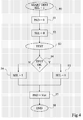
- FIG. 4 is a simplified flow diagram of one embodiment of the protection method according to the invention.
- Positioning for all the circuits connected in parallel for testing by a spike card 1, their respective pads 37 in an inactive state (for example, low).
- test can then begin (block 53, TEST). This test is for example the test conducted conventionally for the type of circuit considered.
- the SEL signal remains in the active default state (step 52 does not succeed).
- test and protection phase is then completed (block 58, END).
- test sequences may be provided.
- an advantage of the above sequence is to allow the use of pad 37 during the test phase.
- the circuits undergo the usual treatments.
- all circuits considered defective have their safety function completely invalid. Indeed, thanks to the breakdown of the fuse, the application of a voltage on the power supply of the circuit will not allow it to start, the signal VAL inactivating permanently and irreversibly, regardless of the subsequent state of the bit SEL , an element essential to the operation of the circuit or at least its secure function.
- the interpretation of the signal VAL or its obtaining logic is such that, after manufacture, the application of a signal on the stud 37 inevitably leads to a blocking of the circuit.
- an attacker manages to access the pad yet inaccessible from outside the integrated circuit it does not allow him to start the circuit or the secure function.
- the default state of the signal SEL is its active state, all the circuits are found for the rest of their life with a switch 38 closed. Therefore, bias the pad 37 in the life of the circuit slams the fuse and blocks the circuit.
- An advantage of the present invention is that the protection element 30 has, because of its simplicity, little risk of itself being defective.
- the active default state of the SEL signal contributes to its security. If necessary, several elements 30 may be provided in parallel to further reduce the risks.
- the present invention is susceptible of various variations and modifications which will be apparent to those skilled in the art.
- the choice of the type of fuse element and the action performed by the protection circuit depends on the application and is within the abilities of those skilled in the art from the functional indications given above.
- the invention has been described in relation to an example in which the integrated circuits are tested in groups, the invention is also applicable if the tests are carried out individually for each circuit of the wafer, the switch of selection 38 and the register 45 then being optional, the programming of the fuse element 31 can be performed by simply applying a signal on the pad 37.
Landscapes
- Engineering & Computer Science (AREA)
- Physics & Mathematics (AREA)
- General Physics & Mathematics (AREA)
- Computer Security & Cryptography (AREA)
- General Engineering & Computer Science (AREA)
- Semiconductor Integrated Circuits (AREA)
- Testing Or Measuring Of Semiconductors Or The Like (AREA)
Applications Claiming Priority (1)
| Application Number | Priority Date | Filing Date | Title |
|---|---|---|---|
| FR0452964A FR2879296A1 (fr) | 2004-12-14 | 2004-12-14 | Invalidation d'un circuit integre |
Publications (1)
| Publication Number | Publication Date |
|---|---|
| EP1674875A1 true EP1674875A1 (de) | 2006-06-28 |
Family
ID=34952147
Family Applications (1)
| Application Number | Title | Priority Date | Filing Date |
|---|---|---|---|
| EP05112078A Withdrawn EP1674875A1 (de) | 2004-12-14 | 2005-12-13 | Sperrung einer integrierten Schaltung |
Country Status (3)
| Country | Link |
|---|---|
| US (1) | US20060124928A1 (de) |
| EP (1) | EP1674875A1 (de) |
| FR (1) | FR2879296A1 (de) |
Citations (6)
| Publication number | Priority date | Publication date | Assignee | Title |
|---|---|---|---|---|
| JPS62136070A (ja) * | 1985-12-09 | 1987-06-19 | Nec Corp | 半導体装置の製造方法 |
| US5671281A (en) * | 1993-03-11 | 1997-09-23 | International Business Machines Corporation | Self modifying access code for altering capabilities |
| EP0920057A2 (de) * | 1989-01-12 | 1999-06-02 | General Instrument Corporation | Schützen eines integrierten Schaltungschips mit einem leitenden Schild |
| US5981971A (en) * | 1997-03-14 | 1999-11-09 | Kabushiki Kaisha Toshiba | Semiconductor ROM wafer test structure, and IC card |
| EP1111618A1 (de) * | 1999-12-22 | 2001-06-27 | Texas Instruments Incorporated | Elektrische Sicherungsarchitektur mit Schutz gegen Lesen und Schreiben |
| JP2001291751A (ja) * | 2000-04-06 | 2001-10-19 | Sony Corp | 半導体装置 |
Family Cites Families (1)
| Publication number | Priority date | Publication date | Assignee | Title |
|---|---|---|---|---|
| US6608792B2 (en) * | 2000-11-09 | 2003-08-19 | Texas Instruments Incorporated | Method and apparatus for storing data in an integrated circuit |
-
2004
- 2004-12-14 FR FR0452964A patent/FR2879296A1/fr not_active Withdrawn
-
2005
- 2005-12-13 EP EP05112078A patent/EP1674875A1/de not_active Withdrawn
- 2005-12-14 US US11/302,620 patent/US20060124928A1/en not_active Abandoned
Patent Citations (6)
| Publication number | Priority date | Publication date | Assignee | Title |
|---|---|---|---|---|
| JPS62136070A (ja) * | 1985-12-09 | 1987-06-19 | Nec Corp | 半導体装置の製造方法 |
| EP0920057A2 (de) * | 1989-01-12 | 1999-06-02 | General Instrument Corporation | Schützen eines integrierten Schaltungschips mit einem leitenden Schild |
| US5671281A (en) * | 1993-03-11 | 1997-09-23 | International Business Machines Corporation | Self modifying access code for altering capabilities |
| US5981971A (en) * | 1997-03-14 | 1999-11-09 | Kabushiki Kaisha Toshiba | Semiconductor ROM wafer test structure, and IC card |
| EP1111618A1 (de) * | 1999-12-22 | 2001-06-27 | Texas Instruments Incorporated | Elektrische Sicherungsarchitektur mit Schutz gegen Lesen und Schreiben |
| JP2001291751A (ja) * | 2000-04-06 | 2001-10-19 | Sony Corp | 半導体装置 |
Non-Patent Citations (2)
| Title |
|---|
| PATENT ABSTRACTS OF JAPAN vol. 011, no. 359 (E - 559) 21 November 1987 (1987-11-21) * |
| PATENT ABSTRACTS OF JAPAN vol. 2002, no. 02 2 April 2002 (2002-04-02) * |
Also Published As
| Publication number | Publication date |
|---|---|
| FR2879296A1 (fr) | 2006-06-16 |
| US20060124928A1 (en) | 2006-06-15 |
Similar Documents
| Publication | Publication Date | Title |
|---|---|---|
| JP4897279B2 (ja) | アーキテクチャを隠し、リバースエンジニアリングを防止し、デバイスを動作不能にするための、電気的にプログラム可能なヒューズの使用 | |
| EP0597745B1 (de) | Sicherungsschaltung für integrierte Schaltung | |
| EP1267248B1 (de) | Geschützte Speicherung von Daten in einer integrierten Schaltung | |
| KR100721895B1 (ko) | 판독/기입 방지의 전기적 퓨즈 구조 | |
| FR2746962A1 (fr) | Dispositif de securite d'une pastille semi-conductrice | |
| CN101965637A (zh) | 具有mosfet熔丝元件的集成电路 | |
| JP2010507255A (ja) | 複数の論理素子を含むワンタイムプログラマブルロジックビット | |
| EP2078304A1 (de) | Verfahren zur bereitstellung optimaler einsatzortprogrammierung von elektronischen schmelzverbindungen | |
| US9762391B2 (en) | Chip authentication technology using carbon nanotubes | |
| US20050212090A1 (en) | Integrated circuit | |
| US20060289658A1 (en) | Processor circuit and method of allocating a logic chip to a memory chip | |
| JP3544168B2 (ja) | 電子装置及びその製造方法 | |
| FR2879296A1 (fr) | Invalidation d'un circuit integre | |
| EP2333703B1 (de) | Elektronische Komponente zum Aufspüren von aktiven Angriffen | |
| US7518899B2 (en) | Method of providing optimal field programming of electronic fuses | |
| FR2960327A1 (fr) | Procede et systeme d'acces a un circuit integre comprenant une cle personnelle d'authentification | |
| Zonenberg et al. | Extraction of Secrets from 40nm {CMOS} Gate Dielectric Breakdown Antifuses by {FIB} Passive Voltage Contrast | |
| CN115878193A (zh) | 一种芯片启动方法及装置 | |
| GB2349491A (en) | Programmable semiconductor device providing security of circuit information | |
| FR2860342A1 (fr) | Circuit integre a dispositif formant capteur de rayonnement | |
| EP3391228A1 (de) | Verfahren zum schreiben in einem nichtflüchtigen speicher einer elektronischen einheit und zugehörige elektronische einheit | |
| EP0675441A1 (de) | Redundante Schmelzsicherungsmatrixanordnung für integrierten Speicher sowie Verfahren zu ihrem Betrieb | |
| US6704676B2 (en) | Method and circuit configuration for identifying an operating property of an integrated circuit | |
| EP1873537A1 (de) | Eignung eines Detektors von Störungspeaks für die Stromzufuhr zu einem integrierten Schaltkreis | |
| EP1715436A2 (de) | Schutz des Ablaufs eines von einem integrierten Schaltkreis ausgeführten Programms oder von Daten, die in diesem Schaltkreis enthalten sind |
Legal Events
| Date | Code | Title | Description |
|---|---|---|---|
| PUAI | Public reference made under article 153(3) epc to a published international application that has entered the european phase |
Free format text: ORIGINAL CODE: 0009012 |
|
| AK | Designated contracting states |
Kind code of ref document: A1 Designated state(s): AT BE BG CH CY CZ DE DK EE ES FI FR GB GR HU IE IS IT LI LT LU LV MC NL PL PT RO SE SI SK TR |
|
| AX | Request for extension of the european patent |
Extension state: AL BA HR MK YU |
|
| AKX | Designation fees paid | ||
| REG | Reference to a national code |
Ref country code: DE Ref legal event code: 8566 |
|
| STAA | Information on the status of an ep patent application or granted ep patent |
Free format text: STATUS: THE APPLICATION IS DEEMED TO BE WITHDRAWN |
|
| 18D | Application deemed to be withdrawn |
Effective date: 20061229 |