EP1672614B1 - Information display device - Google Patents
Information display device Download PDFInfo
- Publication number
- EP1672614B1 EP1672614B1 EP04792068A EP04792068A EP1672614B1 EP 1672614 B1 EP1672614 B1 EP 1672614B1 EP 04792068 A EP04792068 A EP 04792068A EP 04792068 A EP04792068 A EP 04792068A EP 1672614 B1 EP1672614 B1 EP 1672614B1
- Authority
- EP
- European Patent Office
- Prior art keywords
- brightness
- pixel
- type
- illumination
- drawing element
- Prior art date
- Legal status (The legal status is an assumption and is not a legal conclusion. Google has not performed a legal analysis and makes no representation as to the accuracy of the status listed.)
- Expired - Lifetime
Links
- 238000005286 illumination Methods 0.000 claims description 85
- 238000001514 detection method Methods 0.000 claims description 18
- 238000000034 method Methods 0.000 description 17
- 230000008569 process Effects 0.000 description 13
- 238000005516 engineering process Methods 0.000 description 8
- 230000003247 decreasing effect Effects 0.000 description 3
- 239000004973 liquid crystal related substance Substances 0.000 description 3
- 230000008859 change Effects 0.000 description 2
- 238000007796 conventional method Methods 0.000 description 1
- 230000007423 decrease Effects 0.000 description 1
- 238000010586 diagram Methods 0.000 description 1
- 238000005401 electroluminescence Methods 0.000 description 1
- 230000006870 function Effects 0.000 description 1
- 238000009877 rendering Methods 0.000 description 1
- 230000004044 response Effects 0.000 description 1
- 230000008719 thickening Effects 0.000 description 1
Images


Classifications
-
- G—PHYSICS
- G09—EDUCATION; CRYPTOGRAPHY; DISPLAY; ADVERTISING; SEALS
- G09G—ARRANGEMENTS OR CIRCUITS FOR CONTROL OF INDICATING DEVICES USING STATIC MEANS TO PRESENT VARIABLE INFORMATION
- G09G3/00—Control arrangements or circuits, of interest only in connection with visual indicators other than cathode-ray tubes
- G09G3/20—Control arrangements or circuits, of interest only in connection with visual indicators other than cathode-ray tubes for presentation of an assembly of a number of characters, e.g. a page, by composing the assembly by combination of individual elements arranged in a matrix no fixed position being assigned to or needed to be assigned to the individual characters or partial characters
-
- G—PHYSICS
- G09—EDUCATION; CRYPTOGRAPHY; DISPLAY; ADVERTISING; SEALS
- G09G—ARRANGEMENTS OR CIRCUITS FOR CONTROL OF INDICATING DEVICES USING STATIC MEANS TO PRESENT VARIABLE INFORMATION
- G09G5/00—Control arrangements or circuits for visual indicators common to cathode-ray tube indicators and other visual indicators
- G09G5/02—Control arrangements or circuits for visual indicators common to cathode-ray tube indicators and other visual indicators characterised by the way in which colour is displayed
- G09G5/06—Control arrangements or circuits for visual indicators common to cathode-ray tube indicators and other visual indicators characterised by the way in which colour is displayed using colour palettes, e.g. look-up tables
-
- G—PHYSICS
- G09—EDUCATION; CRYPTOGRAPHY; DISPLAY; ADVERTISING; SEALS
- G09G—ARRANGEMENTS OR CIRCUITS FOR CONTROL OF INDICATING DEVICES USING STATIC MEANS TO PRESENT VARIABLE INFORMATION
- G09G5/00—Control arrangements or circuits for visual indicators common to cathode-ray tube indicators and other visual indicators
- G09G5/10—Intensity circuits
-
- G—PHYSICS
- G09—EDUCATION; CRYPTOGRAPHY; DISPLAY; ADVERTISING; SEALS
- G09G—ARRANGEMENTS OR CIRCUITS FOR CONTROL OF INDICATING DEVICES USING STATIC MEANS TO PRESENT VARIABLE INFORMATION
- G09G2320/00—Control of display operating conditions
- G09G2320/02—Improving the quality of display appearance
- G09G2320/0285—Improving the quality of display appearance using tables for spatial correction of display data
-
- G—PHYSICS
- G09—EDUCATION; CRYPTOGRAPHY; DISPLAY; ADVERTISING; SEALS
- G09G—ARRANGEMENTS OR CIRCUITS FOR CONTROL OF INDICATING DEVICES USING STATIC MEANS TO PRESENT VARIABLE INFORMATION
- G09G2320/00—Control of display operating conditions
- G09G2320/06—Adjustment of display parameters
- G09G2320/0626—Adjustment of display parameters for control of overall brightness
-
- G—PHYSICS
- G09—EDUCATION; CRYPTOGRAPHY; DISPLAY; ADVERTISING; SEALS
- G09G—ARRANGEMENTS OR CIRCUITS FOR CONTROL OF INDICATING DEVICES USING STATIC MEANS TO PRESENT VARIABLE INFORMATION
- G09G2320/00—Control of display operating conditions
- G09G2320/06—Adjustment of display parameters
- G09G2320/066—Adjustment of display parameters for control of contrast
-
- G—PHYSICS
- G09—EDUCATION; CRYPTOGRAPHY; DISPLAY; ADVERTISING; SEALS
- G09G—ARRANGEMENTS OR CIRCUITS FOR CONTROL OF INDICATING DEVICES USING STATIC MEANS TO PRESENT VARIABLE INFORMATION
- G09G2360/00—Aspects of the architecture of display systems
- G09G2360/14—Detecting light within display terminals, e.g. using a single or a plurality of photosensors
- G09G2360/144—Detecting light within display terminals, e.g. using a single or a plurality of photosensors the light being ambient light
-
- G—PHYSICS
- G09—EDUCATION; CRYPTOGRAPHY; DISPLAY; ADVERTISING; SEALS
- G09G—ARRANGEMENTS OR CIRCUITS FOR CONTROL OF INDICATING DEVICES USING STATIC MEANS TO PRESENT VARIABLE INFORMATION
- G09G3/00—Control arrangements or circuits, of interest only in connection with visual indicators other than cathode-ray tubes
- G09G3/20—Control arrangements or circuits, of interest only in connection with visual indicators other than cathode-ray tubes for presentation of an assembly of a number of characters, e.g. a page, by composing the assembly by combination of individual elements arranged in a matrix no fixed position being assigned to or needed to be assigned to the individual characters or partial characters
- G09G3/34—Control arrangements or circuits, of interest only in connection with visual indicators other than cathode-ray tubes for presentation of an assembly of a number of characters, e.g. a page, by composing the assembly by combination of individual elements arranged in a matrix no fixed position being assigned to or needed to be assigned to the individual characters or partial characters by control of light from an independent source
- G09G3/36—Control arrangements or circuits, of interest only in connection with visual indicators other than cathode-ray tubes for presentation of an assembly of a number of characters, e.g. a page, by composing the assembly by combination of individual elements arranged in a matrix no fixed position being assigned to or needed to be assigned to the individual characters or partial characters by control of light from an independent source using liquid crystals
-
- G—PHYSICS
- G09—EDUCATION; CRYPTOGRAPHY; DISPLAY; ADVERTISING; SEALS
- G09G—ARRANGEMENTS OR CIRCUITS FOR CONTROL OF INDICATING DEVICES USING STATIC MEANS TO PRESENT VARIABLE INFORMATION
- G09G5/00—Control arrangements or circuits for visual indicators common to cathode-ray tube indicators and other visual indicators
- G09G5/36—Control arrangements or circuits for visual indicators common to cathode-ray tube indicators and other visual indicators characterised by the display of a graphic pattern, e.g. using an all-points-addressable [APA] memory
Definitions
- the present invention relates to an information display which displays predetermined information on a display screen.
- the conventional technology of this type is disclosed by, for example, Japanese Patent Laid-open Publication No. H6-83287 describing a liquid crystal display detecting the illumination of the surrounding portion of the display screen by an illumination sensor, and largely correcting the brightness of the gray-scale portion of a display target when the detected illumination is large, thereby improving the visibility of the image of a photograph, etc.
- the technology of displaying a character on the above-mentioned liquid crystal display can be the technology (antialiasing) of displaying a smooth and readable character by representing the stroke width of a potion smaller than one pixel as a gray-scale outline of a character.
- US2003/001815 discloses a method for enabling power management of a flat-panel display. The method involves detecting at least one display device power state and adjusting a backlight brightness in a display monitor in response to said detecting said at least one display power state. The method further involves altering the brightness of a display image in order to maintain a display image quality when the backlight is adjusted.
- the present invention has been developed to solve the problems of the conventional technology, and aims at providing an information display capable of improving the visibility of each display target.
- the information display of the present invention displays predetermined information on a display screen, detects the type of each drawing element displayed on the display screen, sets the brightness correction characteristic based on the type, and corrects the brightness for each display target based on the brightness correction characteristic.
- the information display displays predetermined information on a display screen, and includes: a drawing element type detection section adapted to read a type of drawing element for each pixel from a memory, wherein the type of drawing element comprises a character and an image; a characteristic setting section adapted to set the brightness correction characteristic for each pixel of the display screen based on the type of drawing element; a brightness correction section adapted to correct the brightness for each pixel based on the brightness correction characteristic; and an illumination detection section adapted to detect the illumination of the surrounding portion of the display screen, wherein the characteristic setting section is further adapted to set the brightness correction characteristic based on the illumination detected by the illumination detection section and the type of drawing element detected by the drawing element type detection section, wherein the characteristic setting section is further adapted to set the brightness correction characteristic for a pixel whose drawing element type is a character, such that the smaller the illumination detected by the illumination detection section, the smaller the brightness of the gray-scale portion of the outline of a character, wherein the characteristic setting section is further adapted to set the brightness correction characteristic
- the brightness can be corrected for each type of display target of a character, an image, etc. or for each type of drawing element. Therefore, for example, each type of display target or the type of drawing element can be more appropriately corrected than the conventional technology of equally correcting the brightness without considering the type of display target.
- the present invention can successfully improve the visibility of each display target.
- the characteristic setting section can set the brightness correction characteristic such that the smaller the illumination detected by the illumination detection section, the smaller the brightness of the gray-scale portion of the outline of a character.
- the characteristic setting section can set the brightness correction characteristic such that the smaller the illumination detected by the illumination detection section, the smaller the correction of the brightness of the low gray-scale level portion which is equal to or lower than a predetermined brightness value, and the larger the correction of the brightness of the high gray-scale level portion which is larger than the predetermined brightness value.
- the surrounding portion of the display screen when the surrounding portion of the display screen is bright and the illumination of the display screen is sufficiently high, the brightness of the image can be maintained and a natural image can be displayed.
- the surrounding portion of the display screen is dark and the illumination of the display screen is not sufficiently high, the brightness of the low gray-scale level portion is reduced with the brightness of the high gray-scale level portion being enhanced, thereby displaying a high-contrast image to be displayed whose outline can be more easily grasped.
- the memory comprises a VRAM adapted to store a type of drawing element and brightness for each pixel, and the characteristic setting section is further adapted to set the brightness correction characteristic based on the type of drawing element stored in the VRAM, and the brightness correction section is further adapted to correct the brightness stored in the VRAM based on the brightness correction characteristic.
- the predetermined information about the brightness and the type of drawing element are stored in the main memory, and the increase of the load of the CPU can be avoided unlike the method of configuring the brightness correction section and the characteristic setting section by the CPU. Therefore, the consumption of the memory capacity and the calculation cost can be reduced.
- the present invention is preferable when applied to a mobile information terminal having small CPU and memory resources.
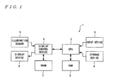
- FIG. 1 is a block diagram showing the outline of the configuration of a mobile information terminal 1.
- the mobile information terminal 1 comprises a central processingunit (CPU) 2, randomaccessmemory (RAM) 3, a storage device 4, an input device 5, a display control device 6, a video RAM (VRAM) 7, a display device 8; and an illumination sensor 9.
- CPU central processingunit
- RAM randomaccessmemory
- VRAM video RAM
- the CPU 2 reads various programs such as a basic control program stored in the storage device 4 and data, processes the programs and data in a work area in the RAM 3, and performs control of each unit provided for the mobile information terminal 1.
- the CPU 2 also reads specified image data from the storage device 4 according to a pressed signal from the input device 5, and outputs the image data to the display control device 6.
- the RAM 3 forms a work area in which each program is processed.
- the RAM 3 also forms a memory area for processing data related to each process executed by CPU 2.
- the storage device 4 stores a basic control program executed by the CPU 2, various application programs, and the data, etc. relating to each program.
- the storage device 4 outputs various programs and data to the CPU 2 according to a read request from the CPU 2.
- Various programs and data in the storage device 4 are stored by the CPU 2 in a readable and executable format.
- the input device 5 comprises a keyboard, etc. having a character key, a number key, and various function keys. When any key of a keyboard is pressed, the input device 5 outputs a pressed signal corresponding to the pressed key to CPU 2.
- the display control device 6 performs the image display process described later, processes the image data output from the CPU 2 into the raster data, and stores the pixel data forming the raster data and the type of drawing element which is the information about the type of drawing element corresponding to the pixel data at the address of the VRAM 7 corresponding to the (x, y) coordinates of the pixel corresponding to each pixel data as shown in FIG. 2 .
- the pixel data indicates the brightness value of each pixel on the display screen of the display device 8 by the values from "0" to "255", and "0" indicates that the brightness of the corresponding pixel is the lowest, and "255" indicates that the brightness of the corresponding pixel is the highest.
- the type of drawing element canbe, for example, a character, an image, a background, etc.
- the outline of a character is represented as a gray-scale portion by antialiasing.
- the VRAM 7 stores the pixel data and the type of drawing element at the addresses corresponding to the (x, y) coordinates of each pixel according to a write request from the display control device 6.
- the VRAM 7 outputs the pixel data and the type of drawing element to the display control device 6 according to a read request from the display control device 6.
- the display device 8 is provided with a display screen such as an electro luminescence display (ELD), a liquid crystal display (LCD), etc., and displays predetermined information comprising a character, an image, etc. according to the pixel data output from the display control device 6.
- ELD electro luminescence display
- LCD liquid crystal display
- FIG. 3 is a flowchart of the image display process executed by the display control device 6.
- the image display process is performed each time a predetermined time passes, and determines in step S101 whether or not image data is output from the CPU 2 as shown in FIG. 3 .
- image data is output (YES)
- control is passed to step S102. If not (NO), control is passed to step S103.
- step S102 the image data output from the CPU 2 is processed into raster data, and the pixel data forming the processed raster data and the type of drawing element corresponding to the pixel data are stored at the addresses of the VRAM 7 corresponding to the (x, y) coordinates of the pixel corresponding to the pixel data, and then control is passed to step S103.
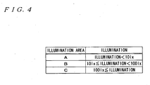
- step S103 the illumination area is determined according to the information about the illumination output from the illumination sensor 9. Practically, as shown in FIG. 4 , when the illumination is smaller than 10 lx, it is defined as an illumination area A (considerably dark environment such as a place under a street-lamp at night).
- illumination area B a rather dark environment such as the corner of a room at night.
- illumination area C a bright environment such as indoor and outdoor in the daytime.
- control is passed to step S104, and the pointer of the VRAM 7 is set at the address corresponding to the leading pixel (0, 0).
- control is passed to step S105 to read the type of drawing element stored at the address set by the pointer of the VRAM 7.
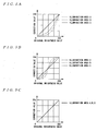
- control is passed to step S106 to select a brightness correction LUT group corresponding to the type of drawing element read in step S105 from among the character LUT group (lookup table) shown in FIG. 5A and FIG. 6 , the image LUT group shown in FIG. 5B , and the background LUT group shown in of FIG. 5C .
- the brightness correction LUT corresponding to the illumination areas A, B, and C detected in step S103 is selected.
- the character LUT group has the correction value of "0" when the brightness value is “0", and the correction value of "255" when the brightness value of "255".
- Each of the illumination areas A, B, and C has a corresponding LUT, and among them, in the LUT corresponding to the illumination area C, the correction value linearly increases with an increasing brightness value at the brightness value from “0" to "255".
- the LUT corresponding to the illumination area B appears as a convex curve under the increase with an increasing inclination with an increasing brightness value at the brightness value from "0" to "255".
- the LUT corresponding to the illumination area A has a smaller brightness value than the LUT corresponding to the illumination area B at the brightness value from "0" to "255". It appears as a convex curve under the increase with an increasing brightness value. That is, when the type of drawing element is a character, and when the illumination of the surrounding portion of the display screen decreases, the LUT for decreasing the brightness of the gray-scale portion is set in the brightness correction LUT group.
- the image LUT group also indicates the correction value of "0" at the brightness value of "0", the correction value of "127” at the brightness value of "127”, and the correction value of "255” at the brightness value of "255”.
- the LUT corresponds to each of the illumination areas A, B, and C. Among them, the LUT corresponding to the illumination area C indicates the linear increase of the correction value with an increase of the brightness value at the brightness value from “0" to "255".
- the LUT corresponding to the illumination area B appears as a convex curve under the increase with the increasing inclination when the brightness value increases at the low gray-scale level portion having the brightness value from "0" to "127".
- the correction value is smaller than the LUT corresponding to the illumination area B, appears as a convex curve below the increase with an increasing inclination with the increase of the brightness value.
- the correction value is larger than the LUT corresponding to the illumination area B, and it appears as a convex curve over the increase with a decreasing inclination with the increase of the brightness value. That is, when the type of drawing element is an image, the smaller the illumination of the surrounding portion of the display screen, the smaller brightness of the low gray-scale level portion, and the larger the brightness of the high gray-scale level portion, thus setting the LUT for brightness correction LUT.
- the background LUT group is provided with a LUT corresponding to all illumination areas A, B, and C.
- the LUT indicates the correction value of "0" at the brightness value of "0", and the correction value of "255” at the brightness value of "255".
- the correction value linearly increases with the increasing value of the brightness value. That is, when the type of drawing element is background, the LUT that maintains the brightness value is set as a brightness correction LUT regardless of the illumination of the surrounding portion.
- control is passed to step S107, and the pixel data stored at the address set by the pointer of the VRAM 7 is read.
- the read pixel data is corrected according to the brightness correction LUT selected in step S106.
- control is passed to step S108, and the pixel data corrected in step S107 is output to the display device 8.
- control is passed to step S109, and it is determined whether or not the image can be displayed on all pixels, that is, whether or not the address corresponds to the trailing pixel (for example, when the resolution of the display screen is SVGA (super video graphics array) 800 x 600, it is (799, 599)) for which the pointer is predetermined. Then, the address corresponds to the trailingpixel (YES), the arithmetic operation is terminated. Otherwise (NO), control is passed to step S 110.
- the address corresponds to the trailingpixel
- step S110 the address of the pointer of the VRAM 7 is updated to the address corresponding to the pixel on the right when viewed from the front, and then control is passed to step S105. If there is no pixel on the right when viewed from the front, the address is updated to the address corresponding to the pixel on the left of the pixel group one row below when viewed from the front. Then, the operations of the mobile information terminal 1 according to the present embodiment are explained below based on the practical situation.
- step S101 the determination in step S101 is "NO"
- step S103 the illumination area A is detected according to the information about the illumination output from the illumination sensor 9.
- step S104 as shown in FIG. 2 , the pointer of the VRAM 7 is set as the address corresponding to the leading pixel (0, 0).
- step S105 the type of drawing element (background) is read from the VRAM 7 based on the pointer .
- step S106 as shown in FIG.
- a background LUT is selected based on the type of drawing element.
- step S107 pixel data is read from the VRAM 7 based on the pointer, and the read pixel data is maintained as is based on the brightness correction LUT.
- step S108 the maintained pixel data is output to the display device 8, the determination in step S109 is "NO", the pointer of the VRAM 7 is in step 110 updated, and the above-mentioned flow is repeated from step S105.
- the display device 8 displays the background at the leading pixel (0, 0) based on the output pixel data as shown in FIG. 7A in the display device 8.
- step 105 the type of drawing element (image) is read from the VRAM 7 based on the pointer.
- step S106 the brightness correction LUT corresponding to the illumination area A is selected from the image LUT group based on the type of drawing element.
- step S107 the pixel data is read from the VRAM 7 based on the pointer, and according to the brightness correction LUT, when the read pixel data is low gray-scale level portion, the brightness is corrected to be lower. When it is high gray-scale level portion, the brightness is corrected to be higher.
- step S108 the corrected pixel data is output to the display device 8, and the above-mentioned flow is repeatedly performed from step S105 through steps S109 and S110.
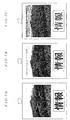
- the display device 8 displays a high-contrast image on the pixel (0, y1) based on the output pixel data as shown in FIG. 7A . If the mobile information terminal 1 is used in a rather dark environment such as the corner of a room at night, and the illumination of the display screen is an illumination area B, then an image lower in contrast than the illumination area A is displayed as shown in FIG. 7B .
- the mobile information terminal 1 is used in a bright environment such as indoor and outdoor in the daytime, and the illumination of the display screen is an illumination area C, then an image whose brightness in the high gray-scale level portion and the low gray-scale level portion is maintained is displayed as shown in FIG. 7C .
- step 105 the type of drawing element (character) is read from the VRAM 7 based on the pointer.
- step S106 the brightness correction LUT corresponding to the illumination area A is selected from the character LUT group based on the type of drawing element.
- step S107 the pixel data is read from the VRAM 7 based on the pointer, and according to the brightness correction LUT, when the readpixel data is a gray-scale portion, the brightness is corrected to be lower.
- step S108 the corrected pixel data is output to the display device 8, and the above-mentioned flow is repeatedly performed from step S105 through steps S109 and S110.
- the display device 8 displays a high-contrast image on the pixel (0, y2) based on the output pixel data as shown in FIG. 7A . If the mobile information terminal 1 is used in a rather dark environment such as the corner of a room at night, and the illumination of the display screen is an illumination area B, then an image lower in contrast than the illumination area A is displayed as shown in FIG. 7B .
- the mobile information terminal 1 is used in a bright environment such as indoor and outdoor in the daytime, and the illumination of the display screen is an illumination area C, then an image whose brightness in the high gray-scale level portion and the low gray-scale level portion is maintained is displayed as shown in FIG. 7C .
- the brightness can be corrected for each type of drawing element of a character, an image, etc. in the module information terminal 1 of the present embodiment. Therefore, for example, the type of drawing element can be more appropriately corrected than the conventional technology of equally correcting the brightness without considering the type of display target.
- the present invention can successfully improve the visibility of each display target as shown in FIGS. 7A to 7C .
- the surrounding portion of the display screen is bright, and the illumination of the display screen is sufficiently high, the brightness of an image is maintained. Therefore, a natural image can be displayed.
- the surrounding portion of the display screen is dark, and the illumination of the display screen is not sufficiently high, the brightness of the low gray-scale level portion is lowered while the brightness of the high gray-scale level portion is enhanced. Therefore, a high-contrast image can be obtained, and an image whose outline as display target is more easily grasped is obtained.
- the surrounding portion of the display screen When the surrounding portion of the display screen is bright, and the illumination of the display screen is sufficiently high, the brightness of the gray-scale portion of the outline of a character is maintained. Therefore, a smooth and readable character can be displayed.
- the surrounding portion of the display screen is dark and the illumination of the display screen is not sufficiently high, the gray-scale portion of the outline of a character is corrected to be smaller. Therefore, the entire character can be deep, and a high-contrast and readable character can be displayed.
- Pixel data and a type of drawing element are stored in the VRAM 7, and the image display process is executed by the display control device 6.
- the load of the CPU 2 can be reduced, thereby reducing the consumption of the memory capacity and the computation cost.
- the conventional method of changing the font itself by thickening the stroke width of a character for smaller illumination after measuring the illumination of the surrounding portion of the display screen by the illumination sensor preparing in advance a plurality of fonts and automatically generating a font are required, thereby largely consuming memory capacity and computation cost.
- step S107 shown in FIG. 3 configures a brightness correction section
- step S105 shown in FIG. 3 configures a drawing element type detection section
- step S106 shown in FIG. 3 configures a characteristic setting section
- the illumination sensor 9 shown in FIG. 1 and step S103 shown in FIG. 3 configure an illumination detection section.
- pixel data and a type of drawing element are stored in the VRAM 7, and the image display process is performed by the display control device 6.
- the present invention is not limited to this application.
- pixel data and a type of drawing element can be stored in the RAM 3, and the image display process can be performed by the CPU 2.
- the display control device 6 and the VRAM 7 can be common units.
- the LUT of y curve and s curve is used as a brightness correction LUT group.
- the present invention is not limited to this application.
- a LUT of a folded line, lifting, indexed, etc. can also be applied.
Landscapes
- Engineering & Computer Science (AREA)
- Physics & Mathematics (AREA)
- Computer Hardware Design (AREA)
- General Physics & Mathematics (AREA)
- Theoretical Computer Science (AREA)
- Control Of Indicators Other Than Cathode Ray Tubes (AREA)
- Controls And Circuits For Display Device (AREA)
- Liquid Crystal Display Device Control (AREA)
Applications Claiming Priority (2)
| Application Number | Priority Date | Filing Date | Title |
|---|---|---|---|
| JP2003348054A JP4175234B2 (ja) | 2003-10-07 | 2003-10-07 | 表示制御装置、携帯型情報端末及び表示制御方法 |
| PCT/JP2004/014657 WO2005036520A1 (ja) | 2003-10-07 | 2004-10-05 | 情報表示装置 |
Publications (3)
| Publication Number | Publication Date |
|---|---|
| EP1672614A1 EP1672614A1 (en) | 2006-06-21 |
| EP1672614A4 EP1672614A4 (en) | 2008-02-20 |
| EP1672614B1 true EP1672614B1 (en) | 2010-01-13 |
Family
ID=34430948
Family Applications (1)
| Application Number | Title | Priority Date | Filing Date |
|---|---|---|---|
| EP04792068A Expired - Lifetime EP1672614B1 (en) | 2003-10-07 | 2004-10-05 | Information display device |
Country Status (7)
| Country | Link |
|---|---|
| US (1) | US7385599B2 (enExample) |
| EP (1) | EP1672614B1 (enExample) |
| JP (1) | JP4175234B2 (enExample) |
| KR (1) | KR100727835B1 (enExample) |
| CN (1) | CN100428329C (enExample) |
| DE (1) | DE602004025129D1 (enExample) |
| WO (1) | WO2005036520A1 (enExample) |
Families Citing this family (9)
| Publication number | Priority date | Publication date | Assignee | Title |
|---|---|---|---|---|
| JP2008197250A (ja) * | 2007-02-09 | 2008-08-28 | Matsushita Electric Ind Co Ltd | 画像処理装置及び画像処理方法 |
| KR20080082279A (ko) | 2007-03-08 | 2008-09-11 | 삼성에스디아이 주식회사 | 유기전계발광표시장치 및 그의 제조방법 |
| KR20110084730A (ko) * | 2010-01-18 | 2011-07-26 | 삼성전자주식회사 | 액정표시장치 및 이의 구동 방법 |
| JP2012253446A (ja) * | 2011-05-31 | 2012-12-20 | Dainippon Printing Co Ltd | 補正装置、補正方法、補正プログラム及び記録媒体 |
| JP5085792B1 (ja) * | 2012-02-08 | 2012-11-28 | シャープ株式会社 | 映像表示装置およびテレビ受信装置 |
| US9208749B2 (en) | 2012-11-13 | 2015-12-08 | Htc Corporation | Electronic device and method for enhancing readability of an image thereof |
| KR102249910B1 (ko) | 2014-05-23 | 2021-05-10 | 삼성전자 주식회사 | 전자 장치 및 이의 출력 특성 제어 방법 |
| KR102744083B1 (ko) * | 2019-08-15 | 2024-12-19 | 엘지전자 주식회사 | 지능형 진단 디바이스 |
| KR20240025097A (ko) * | 2022-08-17 | 2024-02-27 | 삼성디스플레이 주식회사 | 디스플레이 시스템 및 이의 구동 방법 |
Family Cites Families (34)
| Publication number | Priority date | Publication date | Assignee | Title |
|---|---|---|---|---|
| GB1569601A (en) * | 1976-05-18 | 1980-06-18 | Decca Ltd | Pulse radar apparatus |
| AT361608B (de) * | 1979-01-31 | 1981-03-25 | Kretztechnik Gmbh | Verfahren zum markieren bzw. auswerten oder ausmessen von schirmbildern, insbesondere von nach dem ultraschall-impuls-echoverfahren er- zeugten schnittbildern und geraet zur durch- fuehrung dieses verfahrens |
| US4310840A (en) * | 1979-08-27 | 1982-01-12 | Vydec, Inc. | Text-processing |
| US4857899A (en) * | 1985-12-10 | 1989-08-15 | Ascii Corporation | Image display apparatus |
| US4807158A (en) * | 1986-09-30 | 1989-02-21 | Daleco/Ivex Partners, Ltd. | Method and apparatus for sampling images to simulate movement within a multidimensional space |
| US5146592A (en) * | 1987-09-14 | 1992-09-08 | Visual Information Technologies, Inc. | High speed image processing computer with overlapping windows-div |
| US5585926A (en) * | 1991-12-05 | 1996-12-17 | Minolta Co., Ltd. | Document reading apparatus capable of rectifying a picked up image data of documents |
| JPH0683287A (ja) | 1992-09-04 | 1994-03-25 | Sharp Corp | 液晶ディスプレイの表示制御装置 |
| EP0660083B1 (en) * | 1993-12-27 | 2000-09-27 | Aisin Aw Co., Ltd. | Vehicular information display system |
| EP0683596B1 (en) * | 1994-05-18 | 2000-08-30 | Sharp Kabushiki Kaisha | Card type camera with image processing function |
| JPH08307688A (ja) * | 1995-04-28 | 1996-11-22 | Minolta Co Ltd | 画像読み取り装置 |
| GB2305571B8 (en) * | 1995-09-22 | 2000-01-31 | Ibm | Display apparatus with gamma correction |
| JP3614246B2 (ja) * | 1996-05-17 | 2005-01-26 | 株式会社日立製作所 | 画像表示システム,画像表示装置及び画像輝度調整方法 |
| JPH1011025A (ja) * | 1996-06-20 | 1998-01-16 | Nec Corp | 液晶表示装置 |
| JP3631848B2 (ja) * | 1996-06-28 | 2005-03-23 | 富士通株式会社 | 画像表示システム |
| DE69731120T2 (de) * | 1997-04-23 | 2005-02-24 | Thomson Consumer Electronics, Inc., Indianapolis | Bereichs- und informationsanzeigeabhängige videopegelsteuerung |
| US5987624A (en) * | 1997-06-10 | 1999-11-16 | Paradise Electronics, Inc. | Method and apparatus for automatically determining signal parameters of an analog display signal received by a display unit of a computer system |
| AU720015B2 (en) * | 1997-12-18 | 2000-05-18 | Fuji Photo Film Co., Ltd. | Image processing apparatus and method, image synthesizing system and method, image synthesizer and client computer which constitute image synthesizing system, and image separating method |
| US6184861B1 (en) * | 1998-03-24 | 2001-02-06 | Ati Technologies, Inc. | Method and apparatus for processing video and graphics data utilizing intensity scaling |
| US6512507B1 (en) * | 1998-03-31 | 2003-01-28 | Seiko Epson Corporation | Pointing position detection device, presentation system, and method, and computer-readable medium |
| JP3425366B2 (ja) * | 1998-06-30 | 2003-07-14 | シャープ株式会社 | 画像補正装置 |
| JP2000305545A (ja) * | 1999-04-20 | 2000-11-02 | Nec Corp | 画像表示装置 |
| US6346933B1 (en) * | 1999-09-21 | 2002-02-12 | Seiko Epson Corporation | Interactive display presentation system |
| DE60126165T2 (de) * | 2000-02-03 | 2007-10-25 | Sanyo Electric Co., Ltd., Moriguchi | Bildelement-Taktgenerator für eine Anzeige |
| TW518882B (en) * | 2000-03-27 | 2003-01-21 | Hitachi Ltd | Liquid crystal display device for displaying video data |
| EP1148411A3 (en) * | 2000-04-21 | 2005-09-14 | Sony Corporation | Information processing apparatus and method for recognising user gesture |
| US6977630B1 (en) * | 2000-07-18 | 2005-12-20 | University Of Minnesota | Mobility assist device |
| JP2002077723A (ja) * | 2000-09-01 | 2002-03-15 | Minolta Co Ltd | 動画像処理装置、動画像処理方法および記録媒体 |
| JP3971892B2 (ja) * | 2000-09-08 | 2007-09-05 | 株式会社日立製作所 | 液晶表示装置 |
| US6961082B2 (en) * | 2000-11-16 | 2005-11-01 | Fujitsu Limited | Image display control system reducing image transmission delay |
| JP2002196744A (ja) * | 2000-12-25 | 2002-07-12 | Toshiba Corp | 画像表示装置 |
| US7119786B2 (en) | 2001-06-28 | 2006-10-10 | Intel Corporation | Method and apparatus for enabling power management of a flat panel display |
| TWI279657B (en) * | 2001-09-21 | 2007-04-21 | Olympus Corp | Management apparatus |
| US7496228B2 (en) * | 2003-06-13 | 2009-02-24 | Landwehr Val R | Method and system for detecting and classifying objects in images, such as insects and other arthropods |
-
2003
- 2003-10-07 JP JP2003348054A patent/JP4175234B2/ja not_active Expired - Fee Related
-
2004
- 2004-10-05 WO PCT/JP2004/014657 patent/WO2005036520A1/ja not_active Ceased
- 2004-10-05 DE DE602004025129T patent/DE602004025129D1/de not_active Expired - Lifetime
- 2004-10-05 CN CNB2004800020194A patent/CN100428329C/zh not_active Expired - Fee Related
- 2004-10-05 KR KR1020057013829A patent/KR100727835B1/ko not_active Expired - Fee Related
- 2004-10-05 EP EP04792068A patent/EP1672614B1/en not_active Expired - Lifetime
- 2004-10-06 US US10/959,904 patent/US7385599B2/en not_active Expired - Fee Related
Also Published As
| Publication number | Publication date |
|---|---|
| US20050116911A1 (en) | 2005-06-02 |
| JP4175234B2 (ja) | 2008-11-05 |
| WO2005036520A1 (ja) | 2005-04-21 |
| DE602004025129D1 (de) | 2010-03-04 |
| KR100727835B1 (ko) | 2007-06-14 |
| US7385599B2 (en) | 2008-06-10 |
| CN100428329C (zh) | 2008-10-22 |
| EP1672614A1 (en) | 2006-06-21 |
| EP1672614A4 (en) | 2008-02-20 |
| KR20060033706A (ko) | 2006-04-19 |
| CN1723485A (zh) | 2006-01-18 |
| JP2005114958A (ja) | 2005-04-28 |
Similar Documents
| Publication | Publication Date | Title |
|---|---|---|
| US7973973B2 (en) | Display device, display panel driver and method of driving display panel | |
| US10276108B2 (en) | Methods for adjusting backlight brightness levels, related backlight adjusting device, and related display device | |
| US6972771B2 (en) | Image display device, image display method, and image display program | |
| EP3726513A1 (en) | Method, apparatus and device for adjusting backlight brightness according to human eye characteristics | |
| CN108682308A (zh) | 显示面板及其显示方法、显示装置 | |
| US8497887B2 (en) | Display driving unit and method for using the same | |
| JP2002072998A (ja) | 輝度制御装置、輝度調節システム、コンピュータシステム、液晶ディスプレイ装置、輝度制御方法、コンピュータプログラム及び記憶媒体 | |
| EP1672614B1 (en) | Information display device | |
| US20070122061A1 (en) | Image processing device, image processing program, and computer-readable recording medium | |
| JP2010108389A (ja) | 画像表示装置及びプログラム | |
| CN112086055A (zh) | 显示面板的亮度补偿方法、设备和显示装置 | |
| US6927773B2 (en) | Font processing device, terminal device, font processing method, and font processing program | |
| JP4903577B2 (ja) | 映像信号変換装置、映像表示装置 | |
| JP2005114958A5 (enExample) | ||
| CN117953797A (zh) | 显示控制方法、显示控制装置、显示面板及显示装置 | |
| CN102103849B (zh) | 一种osd控制器 | |
| US20050162427A1 (en) | Font processor, terminal device, font processing method, and font processing program | |
| US20100295871A1 (en) | Systems and methods for magnifying display elements | |
| US20050206633A1 (en) | Information display | |
| JP4952704B2 (ja) | 情報表示装置 | |
| JP2001209364A (ja) | 表示装置 | |
| JP2009237438A (ja) | 液晶表示装置 | |
| WO2019239918A1 (ja) | 制御装置、表示装置および制御方法 | |
| US8212929B2 (en) | Image processing method and computer readable medium | |
| JP2004133033A (ja) | 画像表示装置、その制御方法及び制御プログラム |
Legal Events
| Date | Code | Title | Description |
|---|---|---|---|
| PUAI | Public reference made under article 153(3) epc to a published international application that has entered the european phase |
Free format text: ORIGINAL CODE: 0009012 |
|
| 17P | Request for examination filed |
Effective date: 20050620 |
|
| AK | Designated contracting states |
Kind code of ref document: A1 Designated state(s): DE FR GB |
|
| DAX | Request for extension of the european patent (deleted) | ||
| RBV | Designated contracting states (corrected) |
Designated state(s): DE FR GB |
|
| RIC1 | Information provided on ipc code assigned before grant |
Ipc: G09G 3/20 20060101AFI20070330BHEP Ipc: G09G 5/10 20060101ALI20070330BHEP |
|
| A4 | Supplementary search report drawn up and despatched |
Effective date: 20080123 |
|
| 17Q | First examination report despatched |
Effective date: 20080804 |
|
| GRAP | Despatch of communication of intention to grant a patent |
Free format text: ORIGINAL CODE: EPIDOSNIGR1 |
|
| GRAS | Grant fee paid |
Free format text: ORIGINAL CODE: EPIDOSNIGR3 |
|
| GRAA | (expected) grant |
Free format text: ORIGINAL CODE: 0009210 |
|
| AK | Designated contracting states |
Kind code of ref document: B1 Designated state(s): DE FR GB |
|
| REG | Reference to a national code |
Ref country code: GB Ref legal event code: FG4D |
|
| REF | Corresponds to: |
Ref document number: 602004025129 Country of ref document: DE Date of ref document: 20100304 Kind code of ref document: P |
|
| PLBE | No opposition filed within time limit |
Free format text: ORIGINAL CODE: 0009261 |
|
| STAA | Information on the status of an ep patent application or granted ep patent |
Free format text: STATUS: NO OPPOSITION FILED WITHIN TIME LIMIT |
|
| 26N | No opposition filed |
Effective date: 20101014 |
|
| REG | Reference to a national code |
Ref country code: FR Ref legal event code: PLFP Year of fee payment: 12 |
|
| PGFP | Annual fee paid to national office [announced via postgrant information from national office to epo] |
Ref country code: GB Payment date: 20150930 Year of fee payment: 12 |
|
| PGFP | Annual fee paid to national office [announced via postgrant information from national office to epo] |
Ref country code: FR Payment date: 20150908 Year of fee payment: 12 |
|
| PGFP | Annual fee paid to national office [announced via postgrant information from national office to epo] |
Ref country code: DE Payment date: 20150929 Year of fee payment: 12 |
|
| REG | Reference to a national code |
Ref country code: DE Ref legal event code: R119 Ref document number: 602004025129 Country of ref document: DE |
|
| GBPC | Gb: european patent ceased through non-payment of renewal fee |
Effective date: 20161005 |
|
| REG | Reference to a national code |
Ref country code: FR Ref legal event code: ST Effective date: 20170630 |
|
| PG25 | Lapsed in a contracting state [announced via postgrant information from national office to epo] |
Ref country code: DE Free format text: LAPSE BECAUSE OF NON-PAYMENT OF DUE FEES Effective date: 20170503 Ref country code: FR Free format text: LAPSE BECAUSE OF NON-PAYMENT OF DUE FEES Effective date: 20161102 Ref country code: GB Free format text: LAPSE BECAUSE OF NON-PAYMENT OF DUE FEES Effective date: 20161005 |