EP1662547A2 - Flache Lampe - Google Patents
Flache Lampe Download PDFInfo
- Publication number
- EP1662547A2 EP1662547A2 EP05253582A EP05253582A EP1662547A2 EP 1662547 A2 EP1662547 A2 EP 1662547A2 EP 05253582 A EP05253582 A EP 05253582A EP 05253582 A EP05253582 A EP 05253582A EP 1662547 A2 EP1662547 A2 EP 1662547A2
- Authority
- EP
- European Patent Office
- Prior art keywords
- electrode
- electrodes
- electrode portion
- flat lamp
- discharge
- Prior art date
- Legal status (The legal status is an assumption and is not a legal conclusion. Google has not performed a legal analysis and makes no representation as to the accuracy of the status listed.)
- Withdrawn
Links
Images


Classifications
-
- H—ELECTRICITY
- H01—ELECTRIC ELEMENTS
- H01J—ELECTRIC DISCHARGE TUBES OR DISCHARGE LAMPS
- H01J61/00—Gas-discharge or vapour-discharge lamps
- H01J61/02—Details
- H01J61/30—Vessels; Containers
- H01J61/305—Flat vessels or containers
-
- G—PHYSICS
- G02—OPTICS
- G02F—OPTICAL DEVICES OR ARRANGEMENTS FOR THE CONTROL OF LIGHT BY MODIFICATION OF THE OPTICAL PROPERTIES OF THE MEDIA OF THE ELEMENTS INVOLVED THEREIN; NON-LINEAR OPTICS; FREQUENCY-CHANGING OF LIGHT; OPTICAL LOGIC ELEMENTS; OPTICAL ANALOGUE/DIGITAL CONVERTERS
- G02F1/00—Devices or arrangements for the control of the intensity, colour, phase, polarisation or direction of light arriving from an independent light source, e.g. switching, gating or modulating; Non-linear optics
- G02F1/01—Devices or arrangements for the control of the intensity, colour, phase, polarisation or direction of light arriving from an independent light source, e.g. switching, gating or modulating; Non-linear optics for the control of the intensity, phase, polarisation or colour
- G02F1/13—Devices or arrangements for the control of the intensity, colour, phase, polarisation or direction of light arriving from an independent light source, e.g. switching, gating or modulating; Non-linear optics for the control of the intensity, phase, polarisation or colour based on liquid crystals, e.g. single liquid crystal display cells
- G02F1/133—Constructional arrangements; Operation of liquid crystal cells; Circuit arrangements
- G02F1/1333—Constructional arrangements; Manufacturing methods
- G02F1/1335—Structural association of cells with optical devices, e.g. polarisers or reflectors
-
- H—ELECTRICITY
- H01—ELECTRIC ELEMENTS
- H01J—ELECTRIC DISCHARGE TUBES OR DISCHARGE LAMPS
- H01J61/00—Gas-discharge or vapour-discharge lamps
- H01J61/02—Details
- H01J61/04—Electrodes; Screens; Shields
- H01J61/06—Main electrodes
Definitions
- the present invention relates to a flat lamp, and more particularly, to a flat lamp which can improve brightness and luminous efficiency without increasing a discharge voltage.
- Flat lamps which are usually used as back lights for liquid crystal displays (LCDs), have advanced from edge-light or direct-light type flat lamps using conventional cold cathode fluorescent lamps to surface-discharge or facing-discharge type flat lamps in which the entire space below a light emitting surface is a discharge space in consideration of luminous efficiency, uniformity of brightness, and the like.
- a surface-discharge flat lamp has the advantage of having a stable discharge compared to a facing-discharge flat lamp, the entire brightness of the surface discharge flat lamp is inferior to that of the facing-discharge flat lamp.
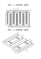
- FIG. 1 illustrates a lower substrate of a conventional surface-discharge type flat lamp.
- a plurality of spacers 15 are arranged to divide a discharge space into a plurality of discharge cells and maintain a constant distance between a lower substrate 10 and an upper substrate (not shown).
- pairs of first and second electrodes 11 and 12 are formed on the lower substrate 10, one pair corresponding to one discharge cell.
- a predetermined voltage is applied to each of the first and second electrodes 11 and 12
- a gas discharge is generated in each of the discharge cells.
- FIG. 2 A flat lamp to solve such problems is illustrated in FIG. 2.
- pairs of first and second electrodes 21 and 22 are formed on a lower substrate 20, one pair corresponding to one discharge cell.
- first and second auxiliary electrodes 23 and 24 are formed between the first and second electrodes 21 and 22.
- the first and second electrodes 21 and 22 are respectively connected to the first and second auxiliary electrodes 23 and 24, through resistance layers 27 and 28, respectively.
- the start of a discharge is initiated by applying a voltage to the first and second auxiliary electrodes 23 and 24.
- such a flat lamp needs an additional process of forming the resistance layers 27 and 28.
- heat loss by the resistance layers 27 and 28 occurs, and a difference in brightness is generated between a portion which has the auxiliary electrodes 23 and 24 and a portion which does not have the auxiliary electrodes 23 and 24.
- a flat lamp comprising: an upper substrate and a lower substrate arranged to face each other and separated by a predetermined distance, with at least one discharge cell formed between the upper and lower substrates; and at least one pair of a first electrode portion and a second electrode portion formed on at least one of the upper and lower substrates, one pair corresponding to one discharge cell, wherein the first electrode portion is composed of an electrode and the second electrode portion is composed of a plurality of electrodes.
- a direct current voltage may be applied between the electrode of the first electrode portion and the electrodes of the second electrode portion.
- the electrode of the first electrode portion may be a cathode electrode and the electrodes of the second electrode portion may be anode electrodes.
- An identical voltage may be applied to the electrodes of the second electrode portion.
- a lower voltage may be applied to the electrode of the second electrode portion closer to the electrode of the first electrode portion.
- the electrodes of the second electrode portion may be connected to each other through a dielectric material and an external voltage may be applied to one of the electrodes of the second electrode portion which is most distant from the electrode of the first electrode portion.
- the discharge cells may be divided by spacers.
- the present invention provides a flat lamp which can improve brightness and luminous efficiency by lengthening a discharge path without increasing a discharge voltage.
- FIG. 3 is an exploded perspective view of a flat lamp according to an embodiment of the present invention.
- FIG. 4 is a view illustrating arrangement of electrodes formed on a bottom surface of a lower substrate of the flat lamp illustrated in FIG. 3.
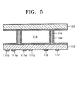
- FIG. 5 is a cross-sectional view of a portion of the flat lamp illustrated in FIG. 3.
- a lower substrate 110 and an upper substrate 120 are arranged to face each other and separated by a predetermined distance.
- the lower substrate 110 and the upper substrate 120 are made of glass.
- At least one discharge cell 115 in which a plasma discharge occurs is formed between the lower substrate 110 and the upper substrate 120.
- the discharge cells 115 are filled with a discharge gas.
- a frame 160 is formed along edges of the lower substrate 110 and the upper substrate 120 such that a space between the lower substrate 110 and the upper substrate 120 is closed.
- At least one spacer 114 is formed between the lower and upper substrates 110 and 120 such that a constant distance between the lower and upper substrates 110 and 120 is maintained and the spacers 114 divide a space between the lower and upper substrates 110 and 120 to form the discharge cells 115.
- Each of the spacers 114 may be formed with its both ends separated from the frame 160 such that each of the discharge cells 115 is partially open.
- each of the spacers 114 may be formed with its one end separated from the frame 160 such that each of the discharge cells 115 is partially open.
- each of the spacers 114 may be formed with its both ends attached to the frame 160 such that each of the discharge cells 115 is closed.
- a fluorescent layer 130 may be formed on inner surfaces of the lower and upper substrates 110 and 120, surfaces of the spacers 114, and an inner surface of the frame 160.
- the fluorescent layer 130 is excited by UV emitted due to the discharge in the discharge cells 115 to emit visible light.
- a plurality of discharge electrodes for generating a discharge in the discharge cells 115 are formed on the bottom surface of the lower substrate 110. Specifically, at least one pair of a first electrode portion and a second electrode portion is formed on the bottom surface of the lower substrate 110, one pair corresponding to one discharge cell 115. Thus, the spacers 114 are disposed between the adjacent first electrode portions and also, between the adjacent second electrode portions.
- the first electrode portion is composed of a first electrode 112 and the second electrode portion is composed of a plurality of second electrodes 111 a and 111 b.
- the second electrode portion may be composed of two electrodes 111 a and 111 b.
- the second electrode portion may be composed of three or more electrodes.
- the entire first electrodes 112 and the entire second electrodes 111 a and 111 b are commonly connected to a first line 118 and a second line 117, respectively. Thus, an identical voltage is applied to the second electrodes 111 a and 111 b formed for all the discharge cells 115.
- a direct current voltage is applied between the first electrode 112 of the first electrode portion and the second electrodes 111a and 111b of the second electrode portion.
- the first electrode 112 may be a cathode electrode and the second electrodes 111 a and 111 b may be anode electrodes.
- a region in which the most amount of input energy is used in the discharge space is a cathode region where a strong electric field is applied and vigorous ionization occurs.
- a glow discharge most of the electrical energy is first used in the cathode region and light energy is generated in a positive column with little electrical energy consumed.
- the first electrode 112 is used as a cathode electrode and the plurality of the second electrodes 111 a and 111 b are used as anode electrodes, thereby increasing brightness and luminous efficiency.
- FIG. 6 is a view illustrating another arrangement of electrodes formed on a bottom surface of a lower substrate 110 of the flat lamp illustrated in FIG. 3.
- the first electrode 112 may be a cathode electrode and the second electrodes 111 a and 111 b may be anode electrodes.
- the second electrodes 111 a and 111 b are connected to each other through a dielectric material 150.
- An external voltage is applied to the second electrode 111 a which is more distant from the first electrode 112 through a second line 117'.
- the entire first electrodes 112 are commonly connected to a first line 18.
- the second electrode portion is composed of two electrodes in the structure illustrated in FIG. 6, the second electrode portion may be composed of three or more electrodes.
- the external voltage may be applied to one of the electrodes of the second electrode portion which is most distant from the first electrode 112.
- FIG. 7 is a cross-sectional view of a portion of a modified example of the flat lamp illustrated in FIG. 3.
- discharge electrodes are formed on a top surface of a lower substrate 110.
- at least one pair of a first electrode portion and a second electrode portion is formed on the top surface of the lower substrate 110, one pair corresponding to one discharge cell 115, and the first electrode portion is composed of a first electrode 112' and the second electrode portion is composed of a plurality of second electrodes 111 a' and 111 b'.
- FIG. 8 is an exploded perspective view of a flat lamp according to an embodiment of the present invention.
- FIG. 9 is a cross-sectional view of a portion of the flat lamp illustrated in FIG. 8.
- portions different from those described in the previous embodiments will be mainly described.
- a lower substrate 210 and an upper substrate 220 are arranged to face each other and separated by a predetermined distance, with at least one discharge cell 215 formed between the lower substrate 210 and the upper substrate 220.
- a frame 260 is formed such that a space between the lower substrate 210 and the upper substrate 220 is closed.
- At least one spacer 214 is formed between the lower and upper substrates 210 and 220 such that the spacers 114 divide a space between the lower and upper substrates 210 and 220 to form the discharge cells 215.
- a fluorescent layer 230 may be formed on inner surfaces of the lower and upper substrates 210 and 220, surfaces of the spacers 214, and an inner surface of the frame 260.
- At least one pair of a first electrode portion and a second electrode portion is formed on a bottom surface of the lower substrate 210, one pair corresponding to one discharge cell 215, and the first electrode portion is composed of a first electrode 212 and the second electrode portion is composed of a plurality of second electrodes 211 a and 211 b.
- the first electrode 212 may be a cathode electrode and the second electrodes 211 a and 211 b may be anode electrodes.
- the second electrode portion may be composed of two electrodes 211 a and 211 b.
- the second electrode portion may be composed of three or more electrodes.
- the first electrode 212 and the second electrodes 211a and 211 b may be formed on a top surface of the lower substrate 210.
- the entire first electrodes 212 and the entire second electrodes 211 a and 211 b are commonly connected to a first line and a second line (not shown), respectively. In this case, an identical voltage is applied to the second electrodes 211a and 211b.
- the second electrodes 211 a and 211 b may be connected to each other through a dielectric material (not shown), as illustrated in FIG. 6.
- a dielectric material not shown
- an external voltage is applied to the second electrode 211 a which is more distant from the first electrode 212 and a voltage lower than the external voltage is applied to the second electrode 211 b which is closer to the first electrode 212 due to a voltage drop by the dielectric material.
- discharge electrodes are further formed on a top surface of the upper substrate 220.
- pairs of a third electrode portion and a fourth electrode portion are formed on the top surface of the upper substrate 220, one pair corresponding to one discharge cell 215.
- the third electrode portion and the fourth electrode portion correspond to the first electrode portion and the second electrode portion, respectively.
- the third electrode portion is composed of a third electrode 222 and the fourth electrode portion is composed of a plurality of fourth electrodes 221a and 221 b.
- the fourth electrode portion is composed of the same number of electrodes as the second electrode portion.
- the third electrode 222 may a cathode electrode and the fourth electrodes 221a and 221 b may be anode electrodes.
- the third electrode 222 and the fourth electrodes 221 a and 221 b may be formed on a bottom surface of the upper substrate 220.
- the entire third electrode 222 and the entire fourth electrodes 221a and 221 b are commonly connected to a third line and a fourth line (not shown), respectively. In this case, an identical voltage is applied to the fourth electrodes 221a and 221 b.
- the fourth electrodes 221a and 221 b may be connected to each other through a dielectric material (not shown), as illustrated in FIG. 6.
- a dielectric material not shown
- an external voltage is applied to the fourth electrode 221 a which is more distant from the third electrode 222 and a voltage lower than the external voltage is applied to the fourth electrode 221 b which is closer to the third electrode 222 due to a voltage drop by the dielectric material.
- Fig. 10 is a cross-sectional view of a portion of a modified example of the flat lamp illustrated in FIG. 8.
- the number of an electrode 221 of the fourth electrode portion formed on the upper substrate 220 is smaller than the number of the second electrodes 211 a and 211 b of the second electrode portion formed on the lower substrate 210.
- the second electrode portion is composed of two electrodes 211a and 211 b and the fourth electrode portion is composed of the electrode 221 in FIG. 10, the embodiment of the present invention is not limited thereto and the second electrode portion may be composed of three or more electrodes and the fourth electrode portion may be composed of two or more electrodes.
- the fourth electrode portion formed on the upper substrate 220 is composed of the electrodes, of which number is smaller than that of the electrodes of the second electrode portion formed on the lower substrate 210, blocking of visible light emitted toward the upper substrate 220 by the discharge due to the discharge electrodes formed on the upper substrate 220 can be reduced.
- the flat lamp according to the present invention has the following advantages.
- first electrode portion and a second electrode portion are formed on at least one of an upper substrate and a lower substrate, one pair corresponding to one discharge cell, and the first electrode portion is composed of an electrode and the second electrode portion is composed of a plurality of electrodes, a discharge voltage can be reduced and luminous efficiency can be increased.
- the electrode of the first electrode portion functions as a cathode electrode and the electrodes of the second electrode portion function as anode electrodes, and thus, brightness and luminous efficiency can be increased.
- the electrodes of the second electrode portion are connected to each other through a dielectric material, and thus, uniformity of brightness can be increased.
Landscapes
- Physics & Mathematics (AREA)
- Nonlinear Science (AREA)
- Mathematical Physics (AREA)
- Chemical & Material Sciences (AREA)
- Crystallography & Structural Chemistry (AREA)
- General Physics & Mathematics (AREA)
- Optics & Photonics (AREA)
- Vessels And Coating Films For Discharge Lamps (AREA)
Applications Claiming Priority (1)
| Application Number | Priority Date | Filing Date | Title |
|---|---|---|---|
| KR1020040081763A KR100657902B1 (ko) | 2004-10-13 | 2004-10-13 | 평판 램프 |
Publications (2)
| Publication Number | Publication Date |
|---|---|
| EP1662547A2 true EP1662547A2 (de) | 2006-05-31 |
| EP1662547A3 EP1662547A3 (de) | 2007-09-19 |
Family
ID=36088427
Family Applications (1)
| Application Number | Title | Priority Date | Filing Date |
|---|---|---|---|
| EP05253582A Withdrawn EP1662547A3 (de) | 2004-10-13 | 2005-06-10 | Flache Lampe |
Country Status (4)
| Country | Link |
|---|---|
| US (1) | US20060076880A1 (de) |
| EP (1) | EP1662547A3 (de) |
| JP (1) | JP2006114500A (de) |
| KR (1) | KR100657902B1 (de) |
Families Citing this family (3)
| Publication number | Priority date | Publication date | Assignee | Title |
|---|---|---|---|---|
| FR2890232A1 (fr) * | 2005-08-23 | 2007-03-02 | Saint Gobain | Lampe plane a decharge coplanaire et utilisations |
| DE102006026332A1 (de) * | 2006-06-02 | 2007-12-06 | Patent-Treuhand-Gesellschaft für elektrische Glühlampen mbH | Entladungslampe für dielektrisch behinderte Entladungen mit rippenartigen Stützelementen zwischen Bodenplatte und Deckenplatte |
| DE102006026333A1 (de) * | 2006-06-02 | 2007-12-06 | Patent-Treuhand-Gesellschaft für elektrische Glühlampen mbH | Entladungslampe für dielektrisch behinderte Entladungen mit flachem Entladungsgefäß |
Family Cites Families (16)
| Publication number | Priority date | Publication date | Assignee | Title |
|---|---|---|---|---|
| KR950003098B1 (ko) * | 1990-07-31 | 1995-04-01 | 삼성전관 주식회사 | 플라즈마 디스플레이 장치 |
| KR200171939Y1 (ko) * | 1994-10-25 | 2000-03-02 | 손욱 | 면광원장치 |
| WO1998043276A2 (de) * | 1997-03-21 | 1998-10-01 | Patent-Treuhand-Gesellschaft für elektrische Glühlampen mbH | Gasentladungslampe mit dielektrisch behinderten elektroden |
| DE19729175A1 (de) * | 1997-03-21 | 1999-01-14 | Patent Treuhand Ges Fuer Elektrische Gluehlampen Mbh | Flachstrahler |
| HU224147B1 (hu) * | 1997-03-21 | 2005-05-30 | Patent-Treuhand-Gesellschaft für elektrische Glühlampen mbH. | Lapos fénycső háttérvilágításhoz, valamint ilyen fénycsövet tartalmazó világítási rendszer és LCD kijelzős készülék |
| US6043605A (en) * | 1997-07-04 | 2000-03-28 | Samsung Display Devices Co., Ltd. | Plasma display device with auxiliary electrodes and protective layer |
| EP0926705A1 (de) * | 1997-12-23 | 1999-06-30 | Patent-Treuhand-Gesellschaft für elektrische Glühlampen mbH | Flachstrahler mit örtlich modulierter Flächenleuchtdichte |
| DE19843419A1 (de) * | 1998-09-22 | 2000-03-23 | Patent Treuhand Ges Fuer Elektrische Gluehlampen Mbh | Entladungslampe mit dielektrisch behinderten Elektroden |
| DE19845228A1 (de) * | 1998-10-01 | 2000-04-27 | Patent Treuhand Ges Fuer Elektrische Gluehlampen Mbh | Dimmbare Entladungslampe für dielektrisch behinderte Entladungen |
| KR100363260B1 (ko) * | 2000-05-27 | 2002-11-30 | 삼성전자 주식회사 | 면 방전형 ac 평판 램프 |
| KR100662491B1 (ko) * | 2000-12-27 | 2007-01-02 | 엘지.필립스 엘시디 주식회사 | 면발광 램프 및 그 제조방법 |
| KR100778840B1 (ko) * | 2001-03-07 | 2007-11-22 | 엘지.필립스 엘시디 주식회사 | 면발광 램프 및 그 제조방법 |
| KR100438831B1 (ko) * | 2001-11-22 | 2004-07-05 | 삼성전자주식회사 | 플라즈마 평판 램프 |
| KR20030062797A (ko) * | 2002-01-19 | 2003-07-28 | 삼성전자주식회사 | 수평 대향 방전형 평판램프 |
| KR100499137B1 (ko) * | 2002-12-10 | 2005-07-04 | 삼성전자주식회사 | 플랫 램프 및 그 구동방법 |
| EP1562221A3 (de) * | 2003-12-03 | 2008-09-17 | Samsung Electronics Co., Ltd. | Flache Lampe |
-
2004
- 2004-10-13 KR KR1020040081763A patent/KR100657902B1/ko not_active Expired - Fee Related
-
2005
- 2005-06-10 EP EP05253582A patent/EP1662547A3/de not_active Withdrawn
- 2005-08-10 US US11/200,097 patent/US20060076880A1/en not_active Abandoned
- 2005-10-13 JP JP2005298249A patent/JP2006114500A/ja active Pending
Also Published As
| Publication number | Publication date |
|---|---|
| JP2006114500A (ja) | 2006-04-27 |
| KR100657902B1 (ko) | 2006-12-14 |
| US20060076880A1 (en) | 2006-04-13 |
| KR20060032795A (ko) | 2006-04-18 |
| EP1662547A3 (de) | 2007-09-19 |
Similar Documents
| Publication | Publication Date | Title |
|---|---|---|
| US6885151B2 (en) | Flat lamp with horizontal facing electrodes | |
| JP2005347259A (ja) | バックライトアセンブリー | |
| US20060006805A1 (en) | Flat lamp | |
| US6636004B1 (en) | Dimmable discharge lamp for dielectrically impeded discharges | |
| EP1662547A2 (de) | Flache Lampe | |
| KR20060009631A (ko) | 방전효율을 개선한 평판 형광램프 | |
| US20050122044A1 (en) | Flat lamp | |
| US7215079B2 (en) | Flat fluorescent lamp requiring low discharge initiating voltage and backlight unit having uniform brightness | |
| US7294957B2 (en) | Flat lamp | |
| US20050280347A1 (en) | Flat lamp | |
| KR100650491B1 (ko) | 평판형 형광램프 | |
| US7659657B2 (en) | Flat fluorescent lamp with improved capability of luminance and reduced initial operational voltage | |
| KR20050036449A (ko) | 평판 램프 | |
| KR20020012096A (ko) | 평면램프용 교류구동형 플라즈마 소자 및 그 제조방법 | |
| US6967433B2 (en) | Cold cathode fluorescent flat lamp | |
| US20060091809A1 (en) | Flat lamp | |
| JP2006147570A (ja) | 面光源装置及びそれを有するバックライトユニット | |
| JPH08273604A (ja) | 平面蛍光ランプ | |
| US20080265784A1 (en) | Gas excitation light-emitting device | |
| KR100477655B1 (ko) | 방전효율을 개선한 평판 형광램프 | |
| KR200352755Y1 (ko) | 평판형 형광램프 | |
| US20070290599A1 (en) | Flat fluorescent lamp and liquid crystal display device thereof | |
| US20050140259A1 (en) | Flat lamp | |
| CN101064235B (zh) | 平面荧光灯 | |
| KR100642732B1 (ko) | 방전개시 전압을 감소시킨 면발광장치 |
Legal Events
| Date | Code | Title | Description |
|---|---|---|---|
| PUAI | Public reference made under article 153(3) epc to a published international application that has entered the european phase |
Free format text: ORIGINAL CODE: 0009012 |
|
| 17P | Request for examination filed |
Effective date: 20050629 |
|
| AK | Designated contracting states |
Kind code of ref document: A2 Designated state(s): AT BE BG CH CY CZ DE DK EE ES FI FR GB GR HU IE IS IT LI LT LU MC NL PL PT RO SE SI SK TR |
|
| AX | Request for extension of the european patent |
Extension state: AL BA HR LV MK YU |
|
| RIC1 | Information provided on ipc code assigned before grant |
Ipc: H01J 61/30 20060101ALI20070427BHEP Ipc: H01J 61/067 20060101ALI20070427BHEP Ipc: H01J 65/04 20060101AFI20070427BHEP |
|
| PUAL | Search report despatched |
Free format text: ORIGINAL CODE: 0009013 |
|
| AK | Designated contracting states |
Kind code of ref document: A3 Designated state(s): AT BE BG CH CY CZ DE DK EE ES FI FR GB GR HU IE IS IT LI LT LU MC NL PL PT RO SE SI SK TR |
|
| AX | Request for extension of the european patent |
Extension state: AL BA HR LV MK YU |
|
| AKX | Designation fees paid |
Designated state(s): DE |
|
| 17Q | First examination report despatched |
Effective date: 20080704 |
|
| STAA | Information on the status of an ep patent application or granted ep patent |
Free format text: STATUS: THE APPLICATION IS DEEMED TO BE WITHDRAWN |
|
| 18D | Application deemed to be withdrawn |
Effective date: 20081115 |