EP1662547A2 - Flat lamp - Google Patents
Flat lamp Download PDFInfo
- Publication number
- EP1662547A2 EP1662547A2 EP05253582A EP05253582A EP1662547A2 EP 1662547 A2 EP1662547 A2 EP 1662547A2 EP 05253582 A EP05253582 A EP 05253582A EP 05253582 A EP05253582 A EP 05253582A EP 1662547 A2 EP1662547 A2 EP 1662547A2
- Authority
- EP
- European Patent Office
- Prior art keywords
- electrode
- electrodes
- electrode portion
- flat lamp
- discharge
- Prior art date
- Legal status (The legal status is an assumption and is not a legal conclusion. Google has not performed a legal analysis and makes no representation as to the accuracy of the status listed.)
- Withdrawn
Links
- 239000000758 substrate Substances 0.000 claims abstract description 66
- 125000006850 spacer group Chemical group 0.000 claims description 15
- 239000003989 dielectric material Substances 0.000 claims description 10
- 230000002411 adverse Effects 0.000 description 1
- 230000000903 blocking effect Effects 0.000 description 1
- 230000000694 effects Effects 0.000 description 1
- 230000005684 electric field Effects 0.000 description 1
- 239000011521 glass Substances 0.000 description 1
- 239000004973 liquid crystal related substance Substances 0.000 description 1
Images


Classifications
-
- H—ELECTRICITY
- H01—ELECTRIC ELEMENTS
- H01J—ELECTRIC DISCHARGE TUBES OR DISCHARGE LAMPS
- H01J61/00—Gas-discharge or vapour-discharge lamps
- H01J61/02—Details
- H01J61/30—Vessels; Containers
- H01J61/305—Flat vessels or containers
-
- G—PHYSICS
- G02—OPTICS
- G02F—OPTICAL DEVICES OR ARRANGEMENTS FOR THE CONTROL OF LIGHT BY MODIFICATION OF THE OPTICAL PROPERTIES OF THE MEDIA OF THE ELEMENTS INVOLVED THEREIN; NON-LINEAR OPTICS; FREQUENCY-CHANGING OF LIGHT; OPTICAL LOGIC ELEMENTS; OPTICAL ANALOGUE/DIGITAL CONVERTERS
- G02F1/00—Devices or arrangements for the control of the intensity, colour, phase, polarisation or direction of light arriving from an independent light source, e.g. switching, gating or modulating; Non-linear optics
- G02F1/01—Devices or arrangements for the control of the intensity, colour, phase, polarisation or direction of light arriving from an independent light source, e.g. switching, gating or modulating; Non-linear optics for the control of the intensity, phase, polarisation or colour
- G02F1/13—Devices or arrangements for the control of the intensity, colour, phase, polarisation or direction of light arriving from an independent light source, e.g. switching, gating or modulating; Non-linear optics for the control of the intensity, phase, polarisation or colour based on liquid crystals, e.g. single liquid crystal display cells
- G02F1/133—Constructional arrangements; Operation of liquid crystal cells; Circuit arrangements
- G02F1/1333—Constructional arrangements; Manufacturing methods
- G02F1/1335—Structural association of cells with optical devices, e.g. polarisers or reflectors
-
- H—ELECTRICITY
- H01—ELECTRIC ELEMENTS
- H01J—ELECTRIC DISCHARGE TUBES OR DISCHARGE LAMPS
- H01J61/00—Gas-discharge or vapour-discharge lamps
- H01J61/02—Details
- H01J61/04—Electrodes; Screens; Shields
- H01J61/06—Main electrodes
Definitions
- the present invention relates to a flat lamp, and more particularly, to a flat lamp which can improve brightness and luminous efficiency without increasing a discharge voltage.
- Flat lamps which are usually used as back lights for liquid crystal displays (LCDs), have advanced from edge-light or direct-light type flat lamps using conventional cold cathode fluorescent lamps to surface-discharge or facing-discharge type flat lamps in which the entire space below a light emitting surface is a discharge space in consideration of luminous efficiency, uniformity of brightness, and the like.
- a surface-discharge flat lamp has the advantage of having a stable discharge compared to a facing-discharge flat lamp, the entire brightness of the surface discharge flat lamp is inferior to that of the facing-discharge flat lamp.
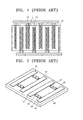
- FIG. 1 illustrates a lower substrate of a conventional surface-discharge type flat lamp.
- a plurality of spacers 15 are arranged to divide a discharge space into a plurality of discharge cells and maintain a constant distance between a lower substrate 10 and an upper substrate (not shown).
- pairs of first and second electrodes 11 and 12 are formed on the lower substrate 10, one pair corresponding to one discharge cell.
- a predetermined voltage is applied to each of the first and second electrodes 11 and 12
- a gas discharge is generated in each of the discharge cells.
- FIG. 2 A flat lamp to solve such problems is illustrated in FIG. 2.
- pairs of first and second electrodes 21 and 22 are formed on a lower substrate 20, one pair corresponding to one discharge cell.
- first and second auxiliary electrodes 23 and 24 are formed between the first and second electrodes 21 and 22.
- the first and second electrodes 21 and 22 are respectively connected to the first and second auxiliary electrodes 23 and 24, through resistance layers 27 and 28, respectively.
- the start of a discharge is initiated by applying a voltage to the first and second auxiliary electrodes 23 and 24.
- such a flat lamp needs an additional process of forming the resistance layers 27 and 28.
- heat loss by the resistance layers 27 and 28 occurs, and a difference in brightness is generated between a portion which has the auxiliary electrodes 23 and 24 and a portion which does not have the auxiliary electrodes 23 and 24.
- a flat lamp comprising: an upper substrate and a lower substrate arranged to face each other and separated by a predetermined distance, with at least one discharge cell formed between the upper and lower substrates; and at least one pair of a first electrode portion and a second electrode portion formed on at least one of the upper and lower substrates, one pair corresponding to one discharge cell, wherein the first electrode portion is composed of an electrode and the second electrode portion is composed of a plurality of electrodes.
- a direct current voltage may be applied between the electrode of the first electrode portion and the electrodes of the second electrode portion.
- the electrode of the first electrode portion may be a cathode electrode and the electrodes of the second electrode portion may be anode electrodes.
- An identical voltage may be applied to the electrodes of the second electrode portion.
- a lower voltage may be applied to the electrode of the second electrode portion closer to the electrode of the first electrode portion.
- the electrodes of the second electrode portion may be connected to each other through a dielectric material and an external voltage may be applied to one of the electrodes of the second electrode portion which is most distant from the electrode of the first electrode portion.
- the discharge cells may be divided by spacers.
- the present invention provides a flat lamp which can improve brightness and luminous efficiency by lengthening a discharge path without increasing a discharge voltage.
- FIG. 3 is an exploded perspective view of a flat lamp according to an embodiment of the present invention.
- FIG. 4 is a view illustrating arrangement of electrodes formed on a bottom surface of a lower substrate of the flat lamp illustrated in FIG. 3.
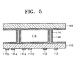
- FIG. 5 is a cross-sectional view of a portion of the flat lamp illustrated in FIG. 3.
- a lower substrate 110 and an upper substrate 120 are arranged to face each other and separated by a predetermined distance.
- the lower substrate 110 and the upper substrate 120 are made of glass.
- At least one discharge cell 115 in which a plasma discharge occurs is formed between the lower substrate 110 and the upper substrate 120.
- the discharge cells 115 are filled with a discharge gas.
- a frame 160 is formed along edges of the lower substrate 110 and the upper substrate 120 such that a space between the lower substrate 110 and the upper substrate 120 is closed.
- At least one spacer 114 is formed between the lower and upper substrates 110 and 120 such that a constant distance between the lower and upper substrates 110 and 120 is maintained and the spacers 114 divide a space between the lower and upper substrates 110 and 120 to form the discharge cells 115.
- Each of the spacers 114 may be formed with its both ends separated from the frame 160 such that each of the discharge cells 115 is partially open.
- each of the spacers 114 may be formed with its one end separated from the frame 160 such that each of the discharge cells 115 is partially open.
- each of the spacers 114 may be formed with its both ends attached to the frame 160 such that each of the discharge cells 115 is closed.
- a fluorescent layer 130 may be formed on inner surfaces of the lower and upper substrates 110 and 120, surfaces of the spacers 114, and an inner surface of the frame 160.
- the fluorescent layer 130 is excited by UV emitted due to the discharge in the discharge cells 115 to emit visible light.
- a plurality of discharge electrodes for generating a discharge in the discharge cells 115 are formed on the bottom surface of the lower substrate 110. Specifically, at least one pair of a first electrode portion and a second electrode portion is formed on the bottom surface of the lower substrate 110, one pair corresponding to one discharge cell 115. Thus, the spacers 114 are disposed between the adjacent first electrode portions and also, between the adjacent second electrode portions.
- the first electrode portion is composed of a first electrode 112 and the second electrode portion is composed of a plurality of second electrodes 111 a and 111 b.
- the second electrode portion may be composed of two electrodes 111 a and 111 b.
- the second electrode portion may be composed of three or more electrodes.
- the entire first electrodes 112 and the entire second electrodes 111 a and 111 b are commonly connected to a first line 118 and a second line 117, respectively. Thus, an identical voltage is applied to the second electrodes 111 a and 111 b formed for all the discharge cells 115.
- a direct current voltage is applied between the first electrode 112 of the first electrode portion and the second electrodes 111a and 111b of the second electrode portion.
- the first electrode 112 may be a cathode electrode and the second electrodes 111 a and 111 b may be anode electrodes.
- a region in which the most amount of input energy is used in the discharge space is a cathode region where a strong electric field is applied and vigorous ionization occurs.
- a glow discharge most of the electrical energy is first used in the cathode region and light energy is generated in a positive column with little electrical energy consumed.
- the first electrode 112 is used as a cathode electrode and the plurality of the second electrodes 111 a and 111 b are used as anode electrodes, thereby increasing brightness and luminous efficiency.
- FIG. 6 is a view illustrating another arrangement of electrodes formed on a bottom surface of a lower substrate 110 of the flat lamp illustrated in FIG. 3.
- the first electrode 112 may be a cathode electrode and the second electrodes 111 a and 111 b may be anode electrodes.
- the second electrodes 111 a and 111 b are connected to each other through a dielectric material 150.
- An external voltage is applied to the second electrode 111 a which is more distant from the first electrode 112 through a second line 117'.
- the entire first electrodes 112 are commonly connected to a first line 18.
- the second electrode portion is composed of two electrodes in the structure illustrated in FIG. 6, the second electrode portion may be composed of three or more electrodes.
- the external voltage may be applied to one of the electrodes of the second electrode portion which is most distant from the first electrode 112.
- FIG. 7 is a cross-sectional view of a portion of a modified example of the flat lamp illustrated in FIG. 3.
- discharge electrodes are formed on a top surface of a lower substrate 110.
- at least one pair of a first electrode portion and a second electrode portion is formed on the top surface of the lower substrate 110, one pair corresponding to one discharge cell 115, and the first electrode portion is composed of a first electrode 112' and the second electrode portion is composed of a plurality of second electrodes 111 a' and 111 b'.
- FIG. 8 is an exploded perspective view of a flat lamp according to an embodiment of the present invention.
- FIG. 9 is a cross-sectional view of a portion of the flat lamp illustrated in FIG. 8.
- portions different from those described in the previous embodiments will be mainly described.
- a lower substrate 210 and an upper substrate 220 are arranged to face each other and separated by a predetermined distance, with at least one discharge cell 215 formed between the lower substrate 210 and the upper substrate 220.
- a frame 260 is formed such that a space between the lower substrate 210 and the upper substrate 220 is closed.
- At least one spacer 214 is formed between the lower and upper substrates 210 and 220 such that the spacers 114 divide a space between the lower and upper substrates 210 and 220 to form the discharge cells 215.
- a fluorescent layer 230 may be formed on inner surfaces of the lower and upper substrates 210 and 220, surfaces of the spacers 214, and an inner surface of the frame 260.
- At least one pair of a first electrode portion and a second electrode portion is formed on a bottom surface of the lower substrate 210, one pair corresponding to one discharge cell 215, and the first electrode portion is composed of a first electrode 212 and the second electrode portion is composed of a plurality of second electrodes 211 a and 211 b.
- the first electrode 212 may be a cathode electrode and the second electrodes 211 a and 211 b may be anode electrodes.
- the second electrode portion may be composed of two electrodes 211 a and 211 b.
- the second electrode portion may be composed of three or more electrodes.
- the first electrode 212 and the second electrodes 211a and 211 b may be formed on a top surface of the lower substrate 210.
- the entire first electrodes 212 and the entire second electrodes 211 a and 211 b are commonly connected to a first line and a second line (not shown), respectively. In this case, an identical voltage is applied to the second electrodes 211a and 211b.
- the second electrodes 211 a and 211 b may be connected to each other through a dielectric material (not shown), as illustrated in FIG. 6.
- a dielectric material not shown
- an external voltage is applied to the second electrode 211 a which is more distant from the first electrode 212 and a voltage lower than the external voltage is applied to the second electrode 211 b which is closer to the first electrode 212 due to a voltage drop by the dielectric material.
- discharge electrodes are further formed on a top surface of the upper substrate 220.
- pairs of a third electrode portion and a fourth electrode portion are formed on the top surface of the upper substrate 220, one pair corresponding to one discharge cell 215.
- the third electrode portion and the fourth electrode portion correspond to the first electrode portion and the second electrode portion, respectively.
- the third electrode portion is composed of a third electrode 222 and the fourth electrode portion is composed of a plurality of fourth electrodes 221a and 221 b.
- the fourth electrode portion is composed of the same number of electrodes as the second electrode portion.
- the third electrode 222 may a cathode electrode and the fourth electrodes 221a and 221 b may be anode electrodes.
- the third electrode 222 and the fourth electrodes 221 a and 221 b may be formed on a bottom surface of the upper substrate 220.
- the entire third electrode 222 and the entire fourth electrodes 221a and 221 b are commonly connected to a third line and a fourth line (not shown), respectively. In this case, an identical voltage is applied to the fourth electrodes 221a and 221 b.
- the fourth electrodes 221a and 221 b may be connected to each other through a dielectric material (not shown), as illustrated in FIG. 6.
- a dielectric material not shown
- an external voltage is applied to the fourth electrode 221 a which is more distant from the third electrode 222 and a voltage lower than the external voltage is applied to the fourth electrode 221 b which is closer to the third electrode 222 due to a voltage drop by the dielectric material.
- Fig. 10 is a cross-sectional view of a portion of a modified example of the flat lamp illustrated in FIG. 8.
- the number of an electrode 221 of the fourth electrode portion formed on the upper substrate 220 is smaller than the number of the second electrodes 211 a and 211 b of the second electrode portion formed on the lower substrate 210.
- the second electrode portion is composed of two electrodes 211a and 211 b and the fourth electrode portion is composed of the electrode 221 in FIG. 10, the embodiment of the present invention is not limited thereto and the second electrode portion may be composed of three or more electrodes and the fourth electrode portion may be composed of two or more electrodes.
- the fourth electrode portion formed on the upper substrate 220 is composed of the electrodes, of which number is smaller than that of the electrodes of the second electrode portion formed on the lower substrate 210, blocking of visible light emitted toward the upper substrate 220 by the discharge due to the discharge electrodes formed on the upper substrate 220 can be reduced.
- the flat lamp according to the present invention has the following advantages.
- first electrode portion and a second electrode portion are formed on at least one of an upper substrate and a lower substrate, one pair corresponding to one discharge cell, and the first electrode portion is composed of an electrode and the second electrode portion is composed of a plurality of electrodes, a discharge voltage can be reduced and luminous efficiency can be increased.
- the electrode of the first electrode portion functions as a cathode electrode and the electrodes of the second electrode portion function as anode electrodes, and thus, brightness and luminous efficiency can be increased.
- the electrodes of the second electrode portion are connected to each other through a dielectric material, and thus, uniformity of brightness can be increased.
Abstract
Description
- The present invention relates to a flat lamp, and more particularly, to a flat lamp which can improve brightness and luminous efficiency without increasing a discharge voltage.
- Flat lamps which are usually used as back lights for liquid crystal displays (LCDs), have advanced from edge-light or direct-light type flat lamps using conventional cold cathode fluorescent lamps to surface-discharge or facing-discharge type flat lamps in which the entire space below a light emitting surface is a discharge space in consideration of luminous efficiency, uniformity of brightness, and the like. Although a surface-discharge flat lamp has the advantage of having a stable discharge compared to a facing-discharge flat lamp, the entire brightness of the surface discharge flat lamp is inferior to that of the facing-discharge flat lamp.
- FIG. 1 illustrates a lower substrate of a conventional surface-discharge type flat lamp. Referring to FIG. 1, a plurality of
spacers 15 are arranged to divide a discharge space into a plurality of discharge cells and maintain a constant distance between alower substrate 10 and an upper substrate (not shown). In addition, pairs of first andsecond electrodes lower substrate 10, one pair corresponding to one discharge cell. In such a structure, when a predetermined voltage is applied to each of the first andsecond electrodes - In general, when a gas discharge is used, luminous efficiency increases as a discharge path is longer. However, an increased discharge path creates an increase in a discharge voltage and has an adverse effect on the cost and lifetime of the flat lamp. Therefore, in the conventional flat lamp with the above-described structure, when making the discharge path long by placing the first and
second electrodes - A flat lamp to solve such problems is illustrated in FIG. 2. Referring to FIG. 2, pairs of first and
second electrodes lower substrate 20, one pair corresponding to one discharge cell. In addition, first and secondauxiliary electrodes second electrodes second electrodes auxiliary electrodes resistance layers auxiliary electrodes resistance layers resistance layers auxiliary electrodes auxiliary electrodes - According to an aspect of the present invention, there is provided a flat lamp comprising: an upper substrate and a lower substrate arranged to face each other and separated by a predetermined distance, with at least one discharge cell formed between the upper and lower substrates; and at least one pair of a first electrode portion and a second electrode portion formed on at least one of the upper and lower substrates, one pair corresponding to one discharge cell, wherein the first electrode portion is composed of an electrode and the second electrode portion is composed of a plurality of electrodes.
- A direct current voltage may be applied between the electrode of the first electrode portion and the electrodes of the second electrode portion. The electrode of the first electrode portion may be a cathode electrode and the electrodes of the second electrode portion may be anode electrodes.
- An identical voltage may be applied to the electrodes of the second electrode portion.
- A lower voltage may be applied to the electrode of the second electrode portion closer to the electrode of the first electrode portion. In this case, the electrodes of the second electrode portion may be connected to each other through a dielectric material and an external voltage may be applied to one of the electrodes of the second electrode portion which is most distant from the electrode of the first electrode portion.
- The discharge cells may be divided by spacers.
- The present invention provides a flat lamp which can improve brightness and luminous efficiency by lengthening a discharge path without increasing a discharge voltage.
- The above and other features and advantages of the present invention will become more apparent by describing in detail exemplary embodiments thereof with reference to the attached drawings in which:
- FIG. 1 illustrates a conventional flat lamp;
- FIG. 2 illustrates another conventional flat lamp;
- FIG. 3 is an exploded perspective view of a flat lamp according to an embodiment of the present invention;
- FIG. 4 is a view illustrating an arrangement of electrodes formed on a bottom surface of a lower substrate of the flat lamp illustrated in FIG. 3;
- FIG. 5 is a cross-sectional view of a portion of the flat lamp illustrated in FIG. 3;
- FIG. 6 is a view illustrating another arrangement of electrodes formed on a bottom surface of a lower substrate of the flat lamp illustrated in FIG. 3;
- FIG. 7 is a cross-sectional view of a portion of a modified example of the flat lamp illustrated in FIG. 3
- FIG. 8 is an exploded perspective view of a flat lamp according to an embodiment of the present invention;
- FIG. 9 is a cross-sectional view of a portion of the flat lamp illustrated in FIG. 8; and
- Fig. 10 is a cross-sectional view of a portion of a modified example of the flat lamp illustrated in FIG. 8.
- Hereinafter, exemplary embodiments of the present invention will be described in more detail with reference to the attached drawings. Like reference numerals in the drawings denote like elements.
- FIG. 3 is an exploded perspective view of a flat lamp according to an embodiment of the present invention. FIG. 4 is a view illustrating arrangement of electrodes formed on a bottom surface of a lower substrate of the flat lamp illustrated in FIG. 3. FIG. 5 is a cross-sectional view of a portion of the flat lamp illustrated in FIG. 3.
- Referring to FIGS. 3 and 5, a
lower substrate 110 and anupper substrate 120 are arranged to face each other and separated by a predetermined distance. In general, thelower substrate 110 and theupper substrate 120 are made of glass. At least onedischarge cell 115 in which a plasma discharge occurs is formed between thelower substrate 110 and theupper substrate 120. Thedischarge cells 115 are filled with a discharge gas. A frame 160 is formed along edges of thelower substrate 110 and theupper substrate 120 such that a space between thelower substrate 110 and theupper substrate 120 is closed. - At least one
spacer 114 is formed between the lower andupper substrates upper substrates spacers 114 divide a space between the lower andupper substrates discharge cells 115. Each of thespacers 114 may be formed with its both ends separated from the frame 160 such that each of thedischarge cells 115 is partially open. Alternatively, each of thespacers 114 may be formed with its one end separated from the frame 160 such that each of thedischarge cells 115 is partially open. Alternatively, each of thespacers 114 may be formed with its both ends attached to the frame 160 such that each of thedischarge cells 115 is closed. - A
fluorescent layer 130 may be formed on inner surfaces of the lower andupper substrates spacers 114, and an inner surface of the frame 160. Thefluorescent layer 130 is excited by UV emitted due to the discharge in thedischarge cells 115 to emit visible light. - Referring to FIG. 4, a plurality of discharge electrodes for generating a discharge in the
discharge cells 115 are formed on the bottom surface of thelower substrate 110. Specifically, at least one pair of a first electrode portion and a second electrode portion is formed on the bottom surface of thelower substrate 110, one pair corresponding to onedischarge cell 115. Thus, thespacers 114 are disposed between the adjacent first electrode portions and also, between the adjacent second electrode portions. The first electrode portion is composed of afirst electrode 112 and the second electrode portion is composed of a plurality ofsecond electrodes electrodes first electrodes 112 and the entiresecond electrodes first line 118 and asecond line 117, respectively. Thus, an identical voltage is applied to thesecond electrodes discharge cells 115. - A direct current voltage is applied between the
first electrode 112 of the first electrode portion and thesecond electrodes first electrode 112 may be a cathode electrode and thesecond electrodes first electrode 112 is used as a cathode electrode and the plurality of thesecond electrodes - When a predetermined voltage is applied between the
first electrode 112 which is a cathode electrode and thesecond electrodes first electrode 112 and thesecond electrode 111 b, which are adjacent to each other, for eachdischarge cell 115. When a distance between thefirst electrode 112 and thesecond electrode 111 b is shorter than that in the conventional flat lamp, the discharge voltage can be reduced. In addition, the generated discharge is extended to thesecond electrode 111 a which is more distant from thefirst electrode 112 and as a result, a main discharge occurs between thefirst electrode 112 and thesecond electrodes first electrode 112 and thesecond electrodes - FIG. 6 is a view illustrating another arrangement of electrodes formed on a bottom surface of a
lower substrate 110 of the flat lamp illustrated in FIG. 3. Referring to FIG. 6, pairs of a first electrode portion and a second electrode portion formed on the bottom surface of thelower substrate 110, one pair corresponding to onedischarge cell 115, wherein the first electrode portion is composed of afirst electrode 112 and the second electrode portion is composed of a plurality ofsecond electrodes first electrode 112 may be a cathode electrode and thesecond electrodes second electrodes dielectric material 150. An external voltage is applied to thesecond electrode 111 a which is more distant from thefirst electrode 112 through a second line 117'. The entirefirst electrodes 112 are commonly connected to a first line 18. Although the second electrode portion is composed of two electrodes in the structure illustrated in FIG. 6, the second electrode portion may be composed of three or more electrodes. The external voltage may be applied to one of the electrodes of the second electrode portion which is most distant from thefirst electrode 112. - In the structure illustrated in FIG. 6, when an external voltage, for example, of 3000 V is applied to the
second electrode 111 a which is more distant from thefirst electrode 112, a voltage which is lower than 3000 V, for example, 2500 V is applied to thesecond electrode 111 b which is closer to thefirst electrode 112 due to a voltage drop by thedielectric material 150. When a lower voltage is applied to thesecond electrode 111 b which is closer to thefirst electrode 112 as described above, discharge generated between thefirst electrode 112 and thesecond electrode 111 b which are adjacent to each other can be more smoothly extended to thesecond electrode 111 a than when a voltage applied between thefirst electrode 112 and thesecond electrode 111 b is identical to a voltage applied between thefirst electrode 112 and thesecond electrode 111 a. - FIG. 7 is a cross-sectional view of a portion of a modified example of the flat lamp illustrated in FIG. 3. Referring to FIG. 7, discharge electrodes are formed on a top surface of a
lower substrate 110. Specifically, at least one pair of a first electrode portion and a second electrode portion is formed on the top surface of thelower substrate 110, one pair corresponding to onedischarge cell 115, and the first electrode portion is composed of a first electrode 112' and the second electrode portion is composed of a plurality ofsecond electrodes 111 a' and 111 b'. - FIG. 8 is an exploded perspective view of a flat lamp according to an embodiment of the present invention. FIG. 9 is a cross-sectional view of a portion of the flat lamp illustrated in FIG. 8. Hereinafter, portions different from those described in the previous embodiments will be mainly described.
- Referring to FIGS. 8 and 9, a
lower substrate 210 and anupper substrate 220 are arranged to face each other and separated by a predetermined distance, with at least onedischarge cell 215 formed between thelower substrate 210 and theupper substrate 220. A frame 260 is formed such that a space between thelower substrate 210 and theupper substrate 220 is closed. - At least one
spacer 214 is formed between the lower andupper substrates spacers 114 divide a space between the lower andupper substrates discharge cells 215. Afluorescent layer 230 may be formed on inner surfaces of the lower andupper substrates spacers 214, and an inner surface of the frame 260. - At least one pair of a first electrode portion and a second electrode portion is formed on a bottom surface of the
lower substrate 210, one pair corresponding to onedischarge cell 215, and the first electrode portion is composed of afirst electrode 212 and the second electrode portion is composed of a plurality ofsecond electrodes first electrode 212 may be a cathode electrode and thesecond electrodes electrodes first electrode 212 and thesecond electrodes lower substrate 210. - The entire
first electrodes 212 and the entiresecond electrodes second electrodes - The
second electrodes second electrode 211 a which is more distant from thefirst electrode 212 and a voltage lower than the external voltage is applied to thesecond electrode 211 b which is closer to thefirst electrode 212 due to a voltage drop by the dielectric material. - In the embodiment illustrated in FIGS. 9, discharge electrodes are further formed on a top surface of the
upper substrate 220. Specifically, pairs of a third electrode portion and a fourth electrode portion are formed on the top surface of theupper substrate 220, one pair corresponding to onedischarge cell 215. The third electrode portion and the fourth electrode portion correspond to the first electrode portion and the second electrode portion, respectively. Thus, the third electrode portion is composed of athird electrode 222 and the fourth electrode portion is composed of a plurality offourth electrodes third electrode 222 may a cathode electrode and thefourth electrodes third electrode 222 and thefourth electrodes upper substrate 220. - The entire
third electrode 222 and the entirefourth electrodes fourth electrodes - The
fourth electrodes fourth electrode 221 a which is more distant from thethird electrode 222 and a voltage lower than the external voltage is applied to thefourth electrode 221 b which is closer to thethird electrode 222 due to a voltage drop by the dielectric material. - When the discharge electrodes are formed on both the
lower substrate 210 and theupper substrate 220 as described above, a discharge can be more smoothly generated in thedischarge cells 215, thereby increasing uniformity of brightness. - Fig. 10 is a cross-sectional view of a portion of a modified example of the flat lamp illustrated in FIG. 8.
- Referring to FIG. 10, the number of an
electrode 221 of the fourth electrode portion formed on theupper substrate 220 is smaller than the number of thesecond electrodes lower substrate 210. Although the second electrode portion is composed of twoelectrodes electrode 221 in FIG. 10, the embodiment of the present invention is not limited thereto and the second electrode portion may be composed of three or more electrodes and the fourth electrode portion may be composed of two or more electrodes. When the fourth electrode portion formed on theupper substrate 220 is composed of the electrodes, of which number is smaller than that of the electrodes of the second electrode portion formed on thelower substrate 210, blocking of visible light emitted toward theupper substrate 220 by the discharge due to the discharge electrodes formed on theupper substrate 220 can be reduced. - The flat lamp according to the present invention has the following advantages.
- First, by forming pairs of a first electrode portion and a second electrode portion on at least one of an upper substrate and a lower substrate, one pair corresponding to one discharge cell, and the first electrode portion is composed of an electrode and the second electrode portion is composed of a plurality of electrodes, a discharge voltage can be reduced and luminous efficiency can be increased.
- Second, the electrode of the first electrode portion functions as a cathode electrode and the electrodes of the second electrode portion function as anode electrodes, and thus, brightness and luminous efficiency can be increased.
- Third, the electrodes of the second electrode portion are connected to each other through a dielectric material, and thus, uniformity of brightness can be increased.
- While the present invention has been particularly shown and described with reference to exemplary embodiments thereof, it will be understood by those of ordinary skill in the art that various changes in form and details may be made therein without departing from the scope of the present invention as defined by the following claims.
Claims (23)
- A flat lamp comprising:an upper substrate and a lower substrate arranged to face each other and separated by a predetermined distance, with at least one discharge cell formed between the upper and lower substrates; andat least one pair of a first electrode portion and a second electrode portion formed on at least one of the upper and lower substrates, one pair corresponding to one discharge cell,wherein the first electrode portion is composed of a first electrode and the second electrode portion is composed of a plurality of second electrodes.
- A flat lamp according to claim 1 wherein each of the plurality of second electrodes are spaced at different distances from the first electrode.
- The flat lamp of claim 1 adapted to be driven by a direct current voltage is applied between the electrode of the first electrode portion and the electrodes of the second electrode portion.
- The flat lamp of claim 1, 2 or 3, wherein the electrode of the first electrode portion is a cathode electrode and the electrodes of the second electrode portion are anode electrodes.
- The flat lamp of claim 3 or 4, adapted to provide wherein an identical voltage is applied to the electrodes of the second electrode portion.
- The flat lamp of claim 3 or 4, adapted to provide a lower voltage is applied to the electrode of the second electrode portion closer to the electrode of the first electrode portion.
- The flat lamp of claim 6, wherein the electrodes of the second electrode portion are connected to each other through a dielectric material and an external voltage is applied to one of the electrodes of the second electrode portion which is most distant from the electrode of the first electrode portion.
- The flat lamp of any preceding claim, wherein the discharge cells are divided by spacers.
- The flat lamp of claim 8, wherein the spacers are formed such that each of the discharge cells is closed.
- The flat lamp of claim 8, wherein the spacers are formed such that each of the discharge cells is partially open.
- A flat lamp according to any preceding claim wherein at least one pair of a first electrode portion and a second electrode portion areformed on the lower substrate.
- The flat lamp of any precedimg claim, wherein the number of the second electrodes comprising the second electrode portion is two.
- The flat lamp of any preceding claim, wherein at least one pair of a third electrode portion and a fourth electrode portion is formed on the upper substrate, one pair corresponding to one discharge cell.
- The flat lamp of claim 13, wherein the third electrode portion is composed of a third electrode and the fourth electrode portion is composed of at least one fourth electrode.
- The flat lamp of claim 14, wherein the third electrode portion and the fourth electrode portion correspond to the first electrode portion and the second electrode portion, respectively.
- The flat lamp of claim 14 or 15, wherein the third electrode is a cathode electrode and the fourth electrodes are anode electrodes.
- The flat lamp of any of claims 14 to 16, wherein the number of the fourth electrodes composing the fourth electrode portion is two.
- The flat lamp of any of claims 14 to 16, wherein the number of the fourth electrodes is identical to the number of the second electrodes.
- The flat lamp of any of claims 14 to 16, wherein the number of the fourth electrodes is less than the number of the second electrodes.
- The flat lamp of any of claims 14 to 16, arranged to apply an identical voltage to each of the fourth electrodes.
- The flat lamp of any of claims 14 to 19 wherein the fourth electrodes are spaced from the third electrode with different spacings.
- The flat lamp of claim 20, arranged to apply a lower voltage to the fourth electrode closer to the third electrode.
- The flat lamp of claim 22, wherein the fourth electrodes are connected to each other through a dielectric material and an external voltage is applied to one of the fourth electrodes which is most distant from the third electrode.
Applications Claiming Priority (1)
| Application Number | Priority Date | Filing Date | Title |
|---|---|---|---|
| KR1020040081763A KR100657902B1 (en) | 2004-10-13 | 2004-10-13 | Flat lamp |
Publications (2)
| Publication Number | Publication Date |
|---|---|
| EP1662547A2 true EP1662547A2 (en) | 2006-05-31 |
| EP1662547A3 EP1662547A3 (en) | 2007-09-19 |
Family
ID=36088427
Family Applications (1)
| Application Number | Title | Priority Date | Filing Date |
|---|---|---|---|
| EP05253582A Withdrawn EP1662547A3 (en) | 2004-10-13 | 2005-06-10 | Flat lamp |
Country Status (4)
| Country | Link |
|---|---|
| US (1) | US20060076880A1 (en) |
| EP (1) | EP1662547A3 (en) |
| JP (1) | JP2006114500A (en) |
| KR (1) | KR100657902B1 (en) |
Families Citing this family (3)
| Publication number | Priority date | Publication date | Assignee | Title |
|---|---|---|---|---|
| FR2890232A1 (en) * | 2005-08-23 | 2007-03-02 | Saint Gobain | COPLANAR DISCHARGE PLANE LAMP AND USES THEREFOR |
| DE102006026332A1 (en) * | 2006-06-02 | 2007-12-06 | Patent-Treuhand-Gesellschaft für elektrische Glühlampen mbH | Discharge lamp for dielectrically impeded discharges with rib-like support elements between base plate and ceiling plate |
| DE102006026333A1 (en) * | 2006-06-02 | 2007-12-06 | Patent-Treuhand-Gesellschaft für elektrische Glühlampen mbH | Discharge lamp for dielectrically impeded discharges with flat discharge vessel |
Citations (10)
| Publication number | Priority date | Publication date | Assignee | Title |
|---|---|---|---|---|
| CA2281091A1 (en) * | 1997-03-21 | 1998-10-01 | Patent-Treuhand-Gesellschaft Fuer Elektrische Gluehlampen Mbh | Flat spotlight with discharge separated by a dielectric layer and device for the electrodes into the leading discharge area |
| EP0889499A2 (en) * | 1997-07-04 | 1999-01-07 | Samsung Display Devices Co., Ltd. | Plasma display device |
| US6246171B1 (en) * | 1997-03-21 | 2001-06-12 | Patent-Treuhand-Gesellschaft Fuer Elektrische Gluehlampen Mbh | Gas discharge lamp with dielectrically impeded electrodes |
| US6483255B1 (en) * | 1997-12-23 | 2002-11-19 | Patent-Treuhand-Gesellschaft Fuer Elektrische Gluehlampen Mbh | Gas discharge lamp with separately operating electrode groups |
| US6566810B1 (en) * | 1998-09-22 | 2003-05-20 | Patent-Treuhand-Gesellschaft Fuer Elektrische Gluehlampen Mbh | Discharge lamp with dielectrically inhibited electrodes |
| EP1316987A2 (en) * | 2001-11-22 | 2003-06-04 | Samsung Electronics Co., Ltd. | Plasma flat lamp |
| US20030137237A1 (en) * | 2002-01-19 | 2003-07-24 | Samsung Electronics Co., Ltd. | Flat lamp with horizontal facing electrodes |
| US6636004B1 (en) * | 1998-10-01 | 2003-10-21 | Patent-Treuhand-Gesellschaft Fuer Elektrische Gluehlampen Mbh | Dimmable discharge lamp for dielectrically impeded discharges |
| US20040119420A1 (en) * | 2002-12-10 | 2004-06-24 | Samsung Electronics Co., Ltd. | Flat lamp and method of driving the same |
| EP1562221A2 (en) * | 2003-12-03 | 2005-08-10 | Samsung Electronics Co., Ltd. | Flat lamp |
Family Cites Families (6)
| Publication number | Priority date | Publication date | Assignee | Title |
|---|---|---|---|---|
| KR950003098B1 (en) * | 1990-07-31 | 1995-04-01 | 삼성전관 주식회사 | Plasma display device |
| KR200171939Y1 (en) * | 1994-10-25 | 2000-03-02 | 손욱 | Plane light apparatus |
| HU224147B1 (en) * | 1997-03-21 | 2005-05-30 | Patent-Treuhand-Gesellschaft für elektrische Glühlampen mbH. | Flat fluorescent light for background lighting and liquid crystal display device fitted with said flat fluorescent light |
| KR100363260B1 (en) * | 2000-05-27 | 2002-11-30 | 삼성전자 주식회사 | A surface discharge AC flat lamp |
| KR100662491B1 (en) * | 2000-12-27 | 2007-01-02 | 엘지.필립스 엘시디 주식회사 | Flat luminescence lamp and method for manufacturing the same |
| KR100778840B1 (en) * | 2001-03-07 | 2007-11-22 | 엘지.필립스 엘시디 주식회사 | Flat luminescence lamp and method for manufacturing the same |
-
2004
- 2004-10-13 KR KR1020040081763A patent/KR100657902B1/en not_active IP Right Cessation
-
2005
- 2005-06-10 EP EP05253582A patent/EP1662547A3/en not_active Withdrawn
- 2005-08-10 US US11/200,097 patent/US20060076880A1/en not_active Abandoned
- 2005-10-13 JP JP2005298249A patent/JP2006114500A/en active Pending
Patent Citations (10)
| Publication number | Priority date | Publication date | Assignee | Title |
|---|---|---|---|---|
| CA2281091A1 (en) * | 1997-03-21 | 1998-10-01 | Patent-Treuhand-Gesellschaft Fuer Elektrische Gluehlampen Mbh | Flat spotlight with discharge separated by a dielectric layer and device for the electrodes into the leading discharge area |
| US6246171B1 (en) * | 1997-03-21 | 2001-06-12 | Patent-Treuhand-Gesellschaft Fuer Elektrische Gluehlampen Mbh | Gas discharge lamp with dielectrically impeded electrodes |
| EP0889499A2 (en) * | 1997-07-04 | 1999-01-07 | Samsung Display Devices Co., Ltd. | Plasma display device |
| US6483255B1 (en) * | 1997-12-23 | 2002-11-19 | Patent-Treuhand-Gesellschaft Fuer Elektrische Gluehlampen Mbh | Gas discharge lamp with separately operating electrode groups |
| US6566810B1 (en) * | 1998-09-22 | 2003-05-20 | Patent-Treuhand-Gesellschaft Fuer Elektrische Gluehlampen Mbh | Discharge lamp with dielectrically inhibited electrodes |
| US6636004B1 (en) * | 1998-10-01 | 2003-10-21 | Patent-Treuhand-Gesellschaft Fuer Elektrische Gluehlampen Mbh | Dimmable discharge lamp for dielectrically impeded discharges |
| EP1316987A2 (en) * | 2001-11-22 | 2003-06-04 | Samsung Electronics Co., Ltd. | Plasma flat lamp |
| US20030137237A1 (en) * | 2002-01-19 | 2003-07-24 | Samsung Electronics Co., Ltd. | Flat lamp with horizontal facing electrodes |
| US20040119420A1 (en) * | 2002-12-10 | 2004-06-24 | Samsung Electronics Co., Ltd. | Flat lamp and method of driving the same |
| EP1562221A2 (en) * | 2003-12-03 | 2005-08-10 | Samsung Electronics Co., Ltd. | Flat lamp |
Also Published As
| Publication number | Publication date |
|---|---|
| JP2006114500A (en) | 2006-04-27 |
| EP1662547A3 (en) | 2007-09-19 |
| US20060076880A1 (en) | 2006-04-13 |
| KR20060032795A (en) | 2006-04-18 |
| KR100657902B1 (en) | 2006-12-14 |
Similar Documents
| Publication | Publication Date | Title |
|---|---|---|
| JP4255930B2 (en) | Backlight assembly | |
| EP1615256A1 (en) | Flat lamp | |
| US6885151B2 (en) | Flat lamp with horizontal facing electrodes | |
| US20060017392A1 (en) | Flat fluorescent lamp improving discharge efficiency | |
| US7294957B2 (en) | Flat lamp | |
| EP1662547A2 (en) | Flat lamp | |
| US20050280347A1 (en) | Flat lamp | |
| US6636004B1 (en) | Dimmable discharge lamp for dielectrically impeded discharges | |
| WO2005083745A1 (en) | Flat fluorescent lamp | |
| KR100642652B1 (en) | Flat fluorescent lamp having good discharge uniformity | |
| US20050122044A1 (en) | Flat lamp | |
| US7215079B2 (en) | Flat fluorescent lamp requiring low discharge initiating voltage and backlight unit having uniform brightness | |
| US20060091809A1 (en) | Flat lamp | |
| US7659657B2 (en) | Flat fluorescent lamp with improved capability of luminance and reduced initial operational voltage | |
| JP2006147570A (en) | Surface light source device and back light unit having it | |
| US6967433B2 (en) | Cold cathode fluorescent flat lamp | |
| KR100606168B1 (en) | Flat fluorescent lamp having ultra slim thickness | |
| US7569982B2 (en) | Light source for a flat display | |
| JPH08273604A (en) | Plane fluorescent lamp | |
| KR100477655B1 (en) | Flat fluorescent lamp improving discharge efficiency | |
| US20080265784A1 (en) | Gas excitation light-emitting device | |
| US20060279215A1 (en) | Flat fluorescent lamp | |
| KR100642732B1 (en) | Surface emitting light device with discharge starting voltage decreased | |
| KR200352755Y1 (en) | Flat fluorescent lamp | |
| KR20080016416A (en) | Surface lighting device and backlight unit having the same |
Legal Events
| Date | Code | Title | Description |
|---|---|---|---|
| PUAI | Public reference made under article 153(3) epc to a published international application that has entered the european phase |
Free format text: ORIGINAL CODE: 0009012 |
|
| 17P | Request for examination filed |
Effective date: 20050629 |
|
| AK | Designated contracting states |
Kind code of ref document: A2 Designated state(s): AT BE BG CH CY CZ DE DK EE ES FI FR GB GR HU IE IS IT LI LT LU MC NL PL PT RO SE SI SK TR |
|
| AX | Request for extension of the european patent |
Extension state: AL BA HR LV MK YU |
|
| RIC1 | Information provided on ipc code assigned before grant |
Ipc: H01J 61/30 20060101ALI20070427BHEP Ipc: H01J 61/067 20060101ALI20070427BHEP Ipc: H01J 65/04 20060101AFI20070427BHEP |
|
| PUAL | Search report despatched |
Free format text: ORIGINAL CODE: 0009013 |
|
| AK | Designated contracting states |
Kind code of ref document: A3 Designated state(s): AT BE BG CH CY CZ DE DK EE ES FI FR GB GR HU IE IS IT LI LT LU MC NL PL PT RO SE SI SK TR |
|
| AX | Request for extension of the european patent |
Extension state: AL BA HR LV MK YU |
|
| AKX | Designation fees paid |
Designated state(s): DE |
|
| 17Q | First examination report despatched |
Effective date: 20080704 |
|
| STAA | Information on the status of an ep patent application or granted ep patent |
Free format text: STATUS: THE APPLICATION IS DEEMED TO BE WITHDRAWN |
|
| 18D | Application deemed to be withdrawn |
Effective date: 20081115 |