EP1662470A1 - Driving apparatus, driving method, and display panel driving system - Google Patents
Driving apparatus, driving method, and display panel driving system Download PDFInfo
- Publication number
- EP1662470A1 EP1662470A1 EP04772211A EP04772211A EP1662470A1 EP 1662470 A1 EP1662470 A1 EP 1662470A1 EP 04772211 A EP04772211 A EP 04772211A EP 04772211 A EP04772211 A EP 04772211A EP 1662470 A1 EP1662470 A1 EP 1662470A1
- Authority
- EP
- European Patent Office
- Prior art keywords
- signal
- lines
- video signals
- display panel
- signal lines
- Prior art date
- Legal status (The legal status is an assumption and is not a legal conclusion. Google has not performed a legal analysis and makes no representation as to the accuracy of the status listed.)
- Ceased
Links
Images




Classifications
-
- G—PHYSICS
- G09—EDUCATION; CRYPTOGRAPHY; DISPLAY; ADVERTISING; SEALS
- G09G—ARRANGEMENTS OR CIRCUITS FOR CONTROL OF INDICATING DEVICES USING STATIC MEANS TO PRESENT VARIABLE INFORMATION
- G09G3/00—Control arrangements or circuits, of interest only in connection with visual indicators other than cathode-ray tubes
- G09G3/20—Control arrangements or circuits, of interest only in connection with visual indicators other than cathode-ray tubes for presentation of an assembly of a number of characters, e.g. a page, by composing the assembly by combination of individual elements arranged in a matrix no fixed position being assigned to or needed to be assigned to the individual characters or partial characters
- G09G3/34—Control arrangements or circuits, of interest only in connection with visual indicators other than cathode-ray tubes for presentation of an assembly of a number of characters, e.g. a page, by composing the assembly by combination of individual elements arranged in a matrix no fixed position being assigned to or needed to be assigned to the individual characters or partial characters by control of light from an independent source
- G09G3/36—Control arrangements or circuits, of interest only in connection with visual indicators other than cathode-ray tubes for presentation of an assembly of a number of characters, e.g. a page, by composing the assembly by combination of individual elements arranged in a matrix no fixed position being assigned to or needed to be assigned to the individual characters or partial characters by control of light from an independent source using liquid crystals
-
- G—PHYSICS
- G09—EDUCATION; CRYPTOGRAPHY; DISPLAY; ADVERTISING; SEALS
- G09G—ARRANGEMENTS OR CIRCUITS FOR CONTROL OF INDICATING DEVICES USING STATIC MEANS TO PRESENT VARIABLE INFORMATION
- G09G3/00—Control arrangements or circuits, of interest only in connection with visual indicators other than cathode-ray tubes
- G09G3/20—Control arrangements or circuits, of interest only in connection with visual indicators other than cathode-ray tubes for presentation of an assembly of a number of characters, e.g. a page, by composing the assembly by combination of individual elements arranged in a matrix no fixed position being assigned to or needed to be assigned to the individual characters or partial characters
- G09G3/34—Control arrangements or circuits, of interest only in connection with visual indicators other than cathode-ray tubes for presentation of an assembly of a number of characters, e.g. a page, by composing the assembly by combination of individual elements arranged in a matrix no fixed position being assigned to or needed to be assigned to the individual characters or partial characters by control of light from an independent source
- G09G3/36—Control arrangements or circuits, of interest only in connection with visual indicators other than cathode-ray tubes for presentation of an assembly of a number of characters, e.g. a page, by composing the assembly by combination of individual elements arranged in a matrix no fixed position being assigned to or needed to be assigned to the individual characters or partial characters by control of light from an independent source using liquid crystals
- G09G3/3611—Control of matrices with row and column drivers
- G09G3/3685—Details of drivers for data electrodes
- G09G3/3688—Details of drivers for data electrodes suitable for active matrices only
-
- G—PHYSICS
- G02—OPTICS
- G02F—OPTICAL DEVICES OR ARRANGEMENTS FOR THE CONTROL OF LIGHT BY MODIFICATION OF THE OPTICAL PROPERTIES OF THE MEDIA OF THE ELEMENTS INVOLVED THEREIN; NON-LINEAR OPTICS; FREQUENCY-CHANGING OF LIGHT; OPTICAL LOGIC ELEMENTS; OPTICAL ANALOGUE/DIGITAL CONVERTERS
- G02F1/00—Devices or arrangements for the control of the intensity, colour, phase, polarisation or direction of light arriving from an independent light source, e.g. switching, gating or modulating; Non-linear optics
- G02F1/01—Devices or arrangements for the control of the intensity, colour, phase, polarisation or direction of light arriving from an independent light source, e.g. switching, gating or modulating; Non-linear optics for the control of the intensity, phase, polarisation or colour
- G02F1/13—Devices or arrangements for the control of the intensity, colour, phase, polarisation or direction of light arriving from an independent light source, e.g. switching, gating or modulating; Non-linear optics for the control of the intensity, phase, polarisation or colour based on liquid crystals, e.g. single liquid crystal display cells
- G02F1/133—Constructional arrangements; Operation of liquid crystal cells; Circuit arrangements
-
- G—PHYSICS
- G09—EDUCATION; CRYPTOGRAPHY; DISPLAY; ADVERTISING; SEALS
- G09G—ARRANGEMENTS OR CIRCUITS FOR CONTROL OF INDICATING DEVICES USING STATIC MEANS TO PRESENT VARIABLE INFORMATION
- G09G3/00—Control arrangements or circuits, of interest only in connection with visual indicators other than cathode-ray tubes
- G09G3/20—Control arrangements or circuits, of interest only in connection with visual indicators other than cathode-ray tubes for presentation of an assembly of a number of characters, e.g. a page, by composing the assembly by combination of individual elements arranged in a matrix no fixed position being assigned to or needed to be assigned to the individual characters or partial characters
-
- G—PHYSICS
- G09—EDUCATION; CRYPTOGRAPHY; DISPLAY; ADVERTISING; SEALS
- G09G—ARRANGEMENTS OR CIRCUITS FOR CONTROL OF INDICATING DEVICES USING STATIC MEANS TO PRESENT VARIABLE INFORMATION
- G09G2310/00—Command of the display device
- G09G2310/02—Addressing, scanning or driving the display screen or processing steps related thereto
- G09G2310/0202—Addressing of scan or signal lines
- G09G2310/0218—Addressing of scan or signal lines with collection of electrodes in groups for n-dimensional addressing
-
- G—PHYSICS
- G09—EDUCATION; CRYPTOGRAPHY; DISPLAY; ADVERTISING; SEALS
- G09G—ARRANGEMENTS OR CIRCUITS FOR CONTROL OF INDICATING DEVICES USING STATIC MEANS TO PRESENT VARIABLE INFORMATION
- G09G2310/00—Command of the display device
- G09G2310/02—Addressing, scanning or driving the display screen or processing steps related thereto
- G09G2310/0232—Special driving of display border areas
-
- G—PHYSICS
- G09—EDUCATION; CRYPTOGRAPHY; DISPLAY; ADVERTISING; SEALS
- G09G—ARRANGEMENTS OR CIRCUITS FOR CONTROL OF INDICATING DEVICES USING STATIC MEANS TO PRESENT VARIABLE INFORMATION
- G09G2310/00—Command of the display device
- G09G2310/02—Addressing, scanning or driving the display screen or processing steps related thereto
- G09G2310/0264—Details of driving circuits
- G09G2310/027—Details of drivers for data electrodes, the drivers handling digital grey scale data, e.g. use of D/A converters
-
- G—PHYSICS
- G09—EDUCATION; CRYPTOGRAPHY; DISPLAY; ADVERTISING; SEALS
- G09G—ARRANGEMENTS OR CIRCUITS FOR CONTROL OF INDICATING DEVICES USING STATIC MEANS TO PRESENT VARIABLE INFORMATION
- G09G2310/00—Command of the display device
- G09G2310/02—Addressing, scanning or driving the display screen or processing steps related thereto
- G09G2310/0264—Details of driving circuits
- G09G2310/0297—Special arrangements with multiplexing or demultiplexing of display data in the drivers for data electrodes, in a pre-processing circuitry delivering display data to said drivers or in the matrix panel, e.g. multiplexing plural data signals to one D/A converter or demultiplexing the D/A converter output to multiple columns
Definitions
- the present invention relates to a display panel of the active matrix type, and more particularly to a drive apparatus, a drive method and a display panel drive system which can commonly comply with display panels of various display formats.
- display panels of the active matrix type e.g., liquid crystal panels, etc.
- the number of pixels is increased with realization of high definition devices (display panels).
- a plural pixel simultaneous sampling system in which plural video signal input lines for delivering video signals from the external to the liquid crystal are provided to simultaneously perform sampling of video signals delivered from the plural video signal input lines to deliver the video signals thus sampled to plural pixels.
- the liquid crystal panel When the liquid crystal panel is caused to be driven by the plural pixel simultaneous sampling system, it is possible to obtain sufficient write time of video signal. Accordingly, in display panels of increased pixel number, i.e., relatively high definition active matrix type such as XGA (eXtended Graphic Array: 1024 ⁇ 768), WXGA (Wide eXtended Graphic Array: 1386 ⁇ 768), or SXGA (Super eXtended Graphic Array : 1400 ⁇ 1500), and display panels of increased pixel number, i.e., high definition active matrix type such as SXGA + (Super eXtended Graphic Array PLUS : 1400 ⁇ 1050), UXGA (Ultra eXtended Graphic Array: 1600 ⁇ 1200), Full HD (Full High Definition: 1920 ⁇ 1080), the plural pixel simultaneous sampling system is employed so that write operation of video signals can be satisfactorily executed.
- active matrix type such as XGA (eXtended Graphic Array: 1024 ⁇ 768), WXGA (
- FIG. 1 is a liquid crystal drive system 50 mounted in a liquid crystal projector, which comprises liquid crystal panels 60R, 60B, 60G which are respectively liquid crystal panel for red, liquid crystal panel for green and liquid crystal panel for blue driven by the plural pixel simultaneous sampling system.
- liquid crystal panels 60R, 60B, 60G which are respectively liquid crystal panel for red, liquid crystal panel for green and liquid crystal panel for blue driven by the plural pixel simultaneous sampling system.
- the respective liquid crystal panels 60R, 60G, 60B that the liquid crystal panel drive system 50 has are a liquid crystal panel complying with the XGA format, wherein video signals are simultaneously written by 6 (six) pixels with respect to pixels in a horizontal direction by the plural pixel simultaneous sampling system.
- the liquid crystal panel drive system 50 comprises a DSD (Digital Signal Driver) 51 including a DSD core 51a for implementing gamma correction and/or color unevenness correction, etc. to digital video signals for red (R), digital video signals for green (G) and digital video signal for blue (B) which are delivered from the external, and LCD drivers 52, 53, 54 for converging digital video signals which have been caused to undergo correction processing by the DSD 51 into analog video signals to deliver the analog video signals thus obtained to the respective liquid crystal panels 60R, 60B, 60G.
- the respective liquid crystal panels 60R, 60B, 60G are respectively mounted at liquid crystal panel modules 61R, 61G, 61B along with horizontal drive circuit and vertical drive circuits which are not shown.
- the LCD drivers 51, 52, 53 serve to convert digital video signals delivered from the DSD 51 into analog video signals of which number corresponds to the number of sampling for performing simultaneous sampling of digital video signals delivered from the DSD 51.
- the LCD drivers 52, 53, 54 serve to convert digital video signals delivered into six parallel analog video signals.
- timing pulses for driving the respective liquid panels 60R, 60G, 60B are generated by a TG (Timing Generator) 51b of the DSD 51.
- the liquid crystal panel module 61R is supplied, through video signal supply lines VSIGI to VSIG6, six parallel analog signals which have been converted at the LCD driver 52.
- the liquid crystal panel module 61R comprises groups of sampling switches SW N each comprised of six sampling switches for simultaneously performing sampling of six signal lines 63 among signal lines 63 that the liquid crystal panel 60R has.
- the groups of sampling switches are driven in order of groups of sampling switches SW 1 , SW 2 , ⁇ , SW N-1 , and SW N in accordance with switch pulses delivered from a horizontal drive circuit 62.
- video signals are simultaneously sampled in units of six video signals.
- video signals are written into pixels 64 in the row direction selected by vertical drive circuits (not shown).
- LCD drivers 52, 53, 54 are required by the number of display formats. As a result, there would take place the problem that the cost is increased, and/or the apparatus becomes large-sized.
- An object of the present invention is to apply (provide) a novel drive apparatus and a novel drive method for display panel, and a novel display panel drive system which can eliminate or solve the problems that prior arts as described above have.
- Another object of the present invention is to provide a drive apparatus, a drive method and a display drive panel system which are adapted for avoiding occurrence of ghost and for driving display panels of various display formats.
- the drive apparatus is directed to a drive apparatus adapted for driving a display panel having x ⁇ y number of pixels arranged in a matrix form at intersecting portions of x number of signal lines disposed in a column direction and y number of gate lines disposed in a row direction, which comprises: data arrangement converting means for converting a digital video signal of m bits into data arrangement in conformity with display format of the display panel; first signal processing means for converting the digital video signal of the m bits which has been converted into the data arrangement in conformity with the display format by the data arrangement converting means into parallel analog video signals of p-phase; second signal processing means for developing the analog video signals of the p-phase which have been converted by the first signal processing means into analog video signals of x/k-phase to deliver the analog video signals thus developed to the x/k number of video signal supply lines which have been selected from N number of video signal supply lines; and signal line selecting means for sequentially selecting, one by one, at the same timing, desired signal lines from respective groups of the x
- x, y, p, m, k are natural numbers, and N is natural number which satisfies N ⁇ (x/k).
- the drive method according to the present invention is directed to a drive method of driving a display panel having x ⁇ y number of pixels arranged in a matrix form at intersecting portions of x number of signal lines disposed in a column direction and y number of gate lines disposed in a row direction, which comprises: converting a digital video signal of in bits into data arrangement in conformity with display format of the display panel; converting the digital video signal of the m bits which has been converted into the data arrangement in conformity with the display format into parallel analog video signals of p-phase; developing the analog video signals of the p-phase into analog video signals of x/k-phase to deliver the analog video signals thus developed to the x/k number of video signal supply lines which have been selected from N number of video signal supply lines; sequentially selecting, one by one, at the same timing, desired signal lines from respective groups of the x/k number of signal lines obtained by dividing the x number of signal lines into the k number of signal lines adjacent in the state where they do not overlap with each other; and performing sampling
- x, y, p, m, k are natural numbers, and N is natural number which satisfies N ⁇ (x/k).
- the display panel drive system is directed to a display panel drive system of driving a display panel having x ⁇ y number of pixels arranged in a matrix form at intersecting portions of x number of signal lines disposed in a column direction and y number of gate lines disposed in a row direction, which comprises: a data arrangement converting unit for converting a digital video signal of m bits into data arrangement in conformity with display format of the display panel; a signal processing unit for converting the digital video signal of the m bits which has been converted into the data arrangement in conformity with the display format by the data arrangement converting unit into parallel analog video signals of p-phase; and a display panel module including the display panel having an arbitrary display format, signal processing means for developing the analog video signals of the p-phase which have been converted by the signal processing unit into analog video signals of x/k-phase to deliver the analog video signals thus developed to N number of video signal supply lines, a vertical drive circuit connected to the gate lines and serving to linearly sequentially drive the gate lines to select the
- x, y, p, m, k are natural numbers, and N is natural number which satisfies N ⁇ (x/k).
- the number of pixels which can be written at a time is greatly increased to a degree of, e.g., 100 pixels or more, as compared to the plural pixel simultaneous sampling system of the conventional system. Accordingly, since sufficient write time can be ensured, it becomes possible to realize stable write operation.
- the display panel module is designed so as to comply with the highest definition display format, e.g., Full HD, thereby making it possible to flexibly cope with display panels of any display format only by adjustment of the number of developments of analog video signals, and/or simple adjustment to suitably change timing, etc. of sampling, etc.
- the system configuration can be greatly simplified.
- desired signal lines are sequentially selected, one by one, at the same timing, from the respective groups of signal lines obtained by dividing signal lines of the display panel, thereby making it possible to completely remove occurrence cause of ghost taking place resulting from the fact that video signal is inserted (written) by deviation of phase relationship between video signal and timing pulse also except for video signals which are to be primarily written.
- the liquid crystal panel drive system 1 according to the present invention will be explained by using FIG. 3.
- the liquid crystal panel drive system 1 is provided at, e.g., liquid crystal projector of three plate (panel) type, etc., and comprises, as liquid crystal panel, a liquid crystal panel 9R for red, a liquid crystal panel 9G for green and a liquid crystal panel 9G for blue.
- the liquid crystal panel drive system 1 comprises a DSD (Digital Signal Driver) 2 for implementing a predetermined signal processing to a digital video signal delivered from the external, a Pre Driver 3 for driving the liquid crystal panel 9R, a Post Driver 4, a Pre Driver 5 for driving the liquid crystal panel 9G, a Post Driver 6, a Pre Driver 7 for driving the liquid crystal panel 9B, and a Post Driver 8.
- DSD Digital Signal Driver
- the liquid crystal panel 9R and the Post Driver 4 are caused to be of the module configuration as a liquid crystal panel module 10R along with vertical drive circuit (not shown).
- the liquid crystal panel 9G and the Post-Driver 6 are caused to be of module configuration as a liquid crystal panel module 10G along with vertical drive circuit (not shown).
- the liquid crystal panel 9B and the Post Driver 8 are caused to be of the module configuration as a liquid crystal panel module 10B along with vertical drive circuits (not shown).
- the DSD 2 comprises a DSD core 2a, a memory 2b, and a TG (Timing Generator) 2c.
- the DSD core 2a serves to implement digital signal processing such as gamma correction and/or color unevenness correction, etc. to respective digital video signals of RGB delivered from the external. Respective digital video signals of RGB are delivered from the external as parallel data of 12 bits.
- the numeric value of the 12 bits is based on the fact that video signal is handled by 12 bits in the liquid crystal panel drive system 50 shown as the prior art, and is a value only diverted (used) from a viewpoint of design. Accordingly, it is not necessarily required that this value is 12 bits, and takes m (m is natural number) bits.
- the memory 2b there are stored respective digital video signals of RGB which have been caused to undergo digital signal processing at the DSD core 2a.
- the respective digital video signals of RGB stored in the memory 2b are converted into data arrangement corresponding to display format such as SVGA, XGA, WXGA, SXGA, SXGA+, UXGA, or Full HD, and are respectively delivered to Pre Drivers 3, 5, 7 in parallel as digital data of 12 bits.
- the Pre Driver 3 is supplied, in parallel, with digital video signals R1, R2 of 12 bits.
- the Pre Driver 5 is supplied, in parallel, with digital video signal of 12 bits as digital video signals G1, G2.
- the Pre Driver 7 is supplied, in parallel, with digital video signal of 12 bits as digital video signals B1, B2.
- the Pre Drivers 3, 5, 7 and the liquid crystal panel modules 10R, 10G, 10B are controlled in synchronism with the timing pulse S 1 or S2.
- the Pre Drivers 3, 5, 7 respectively convert digital video signals inputted in parallel from the DSD 2 into analog video signal of p (p is natural number-phase on the basis of the timing pulse S2 synchronous with video signal to respectively deliver those video signals to the Post Drivers 4, 6, 8.
- Pre Drivers 3, 5 7 also respectively generate pre-charge signal (PSIG) delivered to the liquid crystal panels 9R, 9G, 9B, and panel common DC voltage (VCOM).
- PSIG pre-charge signal
- VCOM panel common DC voltage
- liquid crystal panel modules 10R, 10G, 10B Since the respective liquid crystal panel modules 10R, 10G, 10B are all caused to be of the same configuration except for output wavelength regions of liquid crystal panels 9R, 9G, 9B that the respective liquid crystal panel modules 10R, 10G, 10B have, the liquid crystal panel 10R will be explained as representative.
- the liquid crystal panel module 10R comprises Post Driver 4, liquid crystal panel 9R, a vertical drive circuit 12, a pre-charge drive circuit, and a group of signal line select switches 14.
- the Post Driver 4 respectively develops analog video signals of 12 phase delivered from the Pre Driver 3 into video signals corresponding to the number of outputs which comply with display formats such as SVGA, XGA, WXGA, SXGA, SXGA+, UXGA, and/or Full HD on the basis of timing pulse S 1 synchronous with video signal to deliver the video signals thus developed to the liquid crystal panel 9R through video signal supply line VSIG N (N is natural number) and the group of signal line select switches 14.
- the development processing from the analog signals of 12 phase at the Post Driver 4 into video signals corresponding to the number of outputs which comply with the above-described display format is processing based on the sampling system executed in the liquid crystal panel drive system 1.
- the sampling system of the liquid crystal panel drive system 1 is a system of first selecting signal line which will be described later that the liquid crystal panel 9R has by the number of outputs of video signals which have been developed at the Post Driver 4 to subsequently perform, plural times, an operation to write, at a time, at the same timing, video signals developed with respect to selected signal lines to perform sampling with respect to all signal lines.
- This sampling system is called signal line select sampling system.
- the number of video signals developed by the Post Driver 4 on the basis of the signal line select sampling system is relatively determined by the display format of the liquid crystal panel 9R and the number of write operations for writing video signals onto all signal lines of the liquid crystal panel 9R.
- the display format of the liquid crystal panel 9R is high definition display format having large number of pixels, it is necessary to increase the number of developments of video signals. Moreover, when the number of times required for writing video signals onto all signal lines of the liquid crystal panel 9R is decreased, it is required to increase signal lines onto which video signals are to be written at a time. Accordingly, it is necessary to also increase the number of developments of video signals.
- the signal line select sampling system will be explained in detail later.
- the liquid crystal panel 9R comprises plural gate lines 21 wired in a row form, plural signal lines 22 wired in a column form, and pixels 23 disposed at portions where both lines intersect with each other.
- the pixel 23 is composed of Thin Film Transistor (TFT) which is not shown, and liquid crystal cell which is not similarly shown.
- TFT Thin Film Transistor
- the gate electrode of the TFT is connected to corresponding gate line 21, the source electrode thereof is connected to corresponding signal line 22, and the drain electrode thereof is connected to one electrode (pixel electrode) of corresponding liquid crystal cell.
- the other electrode (opposite electrode) of the liquid crystal cell is supplied with panel common DC voltage (VCOM) generated at the Pre Driver 3 as a predetermined opposite potential.
- VCOM panel common DC voltage
- the vertical drive circuit 12 is divided into left and right portions, which are connected to the gate lines 21, and serves to linearly sequentially drive the connected respective gate lines 21 from the both sides thus to select pixels 23 in a row direction.
- the pre-charge drive circuit 13 applies, in advance, prior to write operation of video signal, pre-charge signal (PSIG) delivered from the Pre Driver 3 through pre-charge line (not shown) to respective signal lines 22 to perform pre-charge operation.
- PSIG pre-charge signal
- This pre-charge operation is performed prior to write operation of video signals with respect to respective pixels 23.
- a group of signal line select switches 14 is each comprised of plural switches for performing sampling of video signals delivered from the Post Driver 4 through video signal supply line VSIG N with respect to the signal line 22.
- the plural switches that the group of signal line select switches 14 are switched at the same timing on the basis of timing pulse S1 delivered from TG2c of the DSD2 to repeat such switching operations plural times to thereby perform sampling of video signals with respect to all signal lines 22 that the liquid crystal panel 9R has.
- the video signals which have been caused to undergo sampling with respect to the signal line 22 are written into pixels 23 in the row direction selected by the vertical drive circuit 12.
- N N is natural number
- N N is natural number
- number of video signal supply lines VSIG 1 to VSIG N connected to the Post Driver 4 are respectively connected to the signal lines 22 through switches SW N that the group of signal line select switches 14 have.
- the switches SW N are provided, one by one, at six signal lines 22 adjacent in the state where they do not overlap with each other among the signal lines 22, and serve to select single signal line 22 every time timing pulse S1 is delivered from the group of signal lines with the six signal lines 22 being as unit.
- signal line 22 located at the left end of the group of signal lines is selected at timing by the first timing pulse S1. and signal line adjacent at the right side is selected at the subsequent timing Thus, the remaining four signal lines 22 are selected in sequence.
- signal lines 22 are selected at the same timing as that of the switch SW 1 in order from the left end of the group of six signal lines.
- respective switches SW N are simultaneously operated by timing pulse S1 to select respective one signal lines 22. Accordingly, the number of write operations with respect to all signal lines 22 that the liquid crystal panel 9R has becomes equal to the number of selections of the signal lines 22 by the switch SW N , i.e., six times here.
- the switches SW N may be provided in units of six signal lines as described above with respect to the signal lines 22 that the liquid crystal panel 9R has, and may be provided in units of arbitrary number of signal lines, e.g., in units of four signal lines or in units of eight signal lines. According as the number of signal lines 22 to be selected by the switch SW N is reduced and the number of switches SW N installed or provided is increased, the number of signal lines 22 which can be subject to sampling at a time becomes large. For this reason, it becomes possible to sufficiently ensure write time with respect to the signal line 22.
- Ratios of write time A which can be ensured in the signal line select sampling system of the conventional system with respect to write time B by the plural pixel simultaneous sampling system (write time required in the case where six pixels are caused to undergo simultaneous sampling) are respectively shown in the case where the number of signal lines 22 to be selected is set to 1, 2 , 4, 6, 8 are shown in FIG. 6.
- the number N of switches SW N constituting the group of signal line select switches 14 is determined by the number of signal lines 22 to be selected. For example, if the number of signal lines 22 to be selected becomes small, required number of switches SW N is increased. If the number of signal lines 22 to be selected becomes large, required number of switches SW N is decreased.
- the respective numbers of signal lines 22 cannot be divided in the case where the number of signal lines 22 to be selected by the switch SW N is set to six.
- dummy signal line 22 and dummy pixel are added to the liquid crystal panel 9R in order to comply with one switch SW ⁇ SUB>134 ⁇ /SUB> which has been increased.
- 800 signal lines 22 exist four dummy signal lines 22 are newly required.
- only four dummy pixel number (D) is also added by four in the row direction in correspondence with four dummy signal lines 22 to be newly supplemented.
- the number of horizontal pixels shown in FIG. 7 is the number of horizontal pixels (Ha) in which dummy pixel number (D) is taken into consideration. In FIG. 7, "*" indicates that no dummy pixel is required.
- dummy signal lines 22 and dummy pixels are supplemented to the liquid crystal panel 9R in entirely the same manner to allow the number of horizontal pixels to be the number of horizontal pixels (Ha) as shown in FIG. 7, thereby making it possibly to take matching with the number of switches SW N .
- video signal delivered from the Post Driver 4 to the switch SW N through video signal supply lines VSIG 1 to VSIG N will be explained.
- the video signal delivered from the Post Driver 4 to the switch SW N through video signal supply lines VSIG 1 to VSIG N is a video signal developed from analog video signals of 12-phase at the Post Driver 4.
- sampling of video signal is performed by switching operation by the switch SW N with respect to the signal line 22 of the liquid crystal panel 9R.
- video signals delivered from the Post Driver 4 through video signal supply lines VSIG 1 to VSIG N are also required by the number of switches SW N .
- the Post Driver 4 develops video signals of 12-phase delivered from the Pre Driver 3 by the number of switches SW N determined by the display format of the liquid crystal panel 9R and the number of write operations with respect to the signal line 22 that the liquid crystal panel 9R has to output the video signals thus developed.
- the number of outputs i.e., the number of developments of video signals from the Post Driver 4 every display formats such as SVGA, XGA, WXGA, SXGA, SXGA+, UXGA, Full HD in the case where the number of signal lines 22 to be selected by the switch SW N is set to six is shown in FIG. 8.
- the number of developments of video signals from the Post Driver 4 is determined by the display format of the liquid crystal panel 9R and the number of signal lines 22 to be selected by the switch SW N .
- the total number of developments shown in FIG. 8 indicates the number of developments per one phase of analog video signals of p-phase delivered from the Pre Driver 3 to the Post Driver 4.
- the Post Driver 4 respectively develops analog video signals of 12-phase into analog video signals of 27-phase as shown in FIG. 9A in the Full HD.
- the Post Driver 4 develops the video signals of 12-phase by the total number of developments shown in FIG. 8 to output the video signals thus developed to video signal supply lines VSIG 1 to VSIG N in a manner such that they are thinned as shown in FIGS. 9B, 9C, 9D, 9E, 9F, 9G.
- the number of outputs pins of the Post Driver 4 of the liquid crystal panel module 9R, the number of video signal supply lines VSIG N physically wired and the number of switches SW ⁇ SUB>N ⁇ /SUB> prepared at the group of signal line select switches 14 are designed so as to comply with the highest definition display format, e.g., Full HD to thereby adjust the number of developments of analog video signals of p-phase delivered from the Pre Driver 3 by the Post Driver 4 even in the case where liquid crystal panel of any display format is used thus to have ability to flexibly cope with such situation only by simple adjustment to suitably change timing pulse, etc. by the DSD2.
- the highest definition display format e.g., Full HD
- the video signal which has been developed at the Post Driver 4 and has been delivered to video signal supply lines VSIG 1 to VSIG N is delivered to respective switches SW N that the group of signal line select switches 14 has.
- the video signal thus obtained is delivered to the signal line 22 that each switch SW N selects every time timing pulse S1 is delivered, and is written into pixels 23 on the gate line 21 selected by the vertical drive circuit 12.
- video signals are simultaneously written with respect to pixels arranged at interval of five pixels from pixel of the left end as shown in FIG. 10A at a first timing, and video signals are sequentially written into pixel adjacent at the right side as shown in FIGS. 10B, 10C, 10D, 10E, 10F at the subsequent timings.
- the region of cross lines indicated at a in FIG. 10 indicates pixel which has been already written, and the region of slanting lines indicated at b indicates pixel which has been newly written.
- the signal line select sampling system is executed in entirely the same manner also in the case of the liquid crystal panel 9G driven by the Pre Driver 5 and the Post Driver 6 and/or the liquid crystal panel 9B driven by the Pre Driver 7 and the Post Driver 8.
- the signal line select sampling system executed by the liquid crystal panel drive system 1 since the number of pixels which can be written at a time is greatly increased to a degree, e.g., from six to 100 pixels or more as compared to the plural simultaneous sampling system carried out as the prior art, it is possible to ensure write time which is larger than two times or more. For this reason, stable write operation is performed.
Landscapes
- Engineering & Computer Science (AREA)
- Physics & Mathematics (AREA)
- General Physics & Mathematics (AREA)
- Theoretical Computer Science (AREA)
- Computer Hardware Design (AREA)
- Crystallography & Structural Chemistry (AREA)
- Chemical & Material Sciences (AREA)
- Nonlinear Science (AREA)
- Mathematical Physics (AREA)
- Optics & Photonics (AREA)
- Control Of Indicators Other Than Cathode Ray Tubes (AREA)
- Liquid Crystal Display Device Control (AREA)
- Liquid Crystal (AREA)
- Transforming Electric Information Into Light Information (AREA)
- Video Image Reproduction Devices For Color Tv Systems (AREA)
Abstract
Description
- The present invention relates to a display panel of the active matrix type, and more particularly to a drive apparatus, a drive method and a display panel drive system which can commonly comply with display panels of various display formats.
- This Application claims priority of Japanese Patent Application No. 2003-307921, filed on August 29, 2003, the entirety of which is incorporated by reference herein.
- In display panels of the active matrix type, e.g., liquid crystal panels, etc., there is the trend where the number of pixels is increased with realization of high definition devices (display panels). In the case where the number of pixels is increased in such a way, since write time becomes short in dot sequential drive system where video signals are written by one pixel, there is employed a plural pixel simultaneous sampling system in which plural video signal input lines for delivering video signals from the external to the liquid crystal are provided to simultaneously perform sampling of video signals delivered from the plural video signal input lines to deliver the video signals thus sampled to plural pixels.
- When the liquid crystal panel is caused to be driven by the plural pixel simultaneous sampling system, it is possible to obtain sufficient write time of video signal. Accordingly, in display panels of increased pixel number, i.e., relatively high definition active matrix type such as XGA (eXtended Graphic Array: 1024 × 768), WXGA (Wide eXtended Graphic Array: 1386 × 768), or SXGA (Super eXtended Graphic Array : 1400 × 1500), and display panels of increased pixel number, i.e., high definition active matrix type such as SXGA + (Super eXtended Graphic Array PLUS : 1400 × 1050), UXGA (Ultra eXtended Graphic Array: 1600 × 1200), Full HD (Full High Definition: 1920 × 1080), the plural pixel simultaneous sampling system is employed so that write operation of video signals can be satisfactorily executed.
- The plural pixel simultaneous sampling system for driving the liquid crystal panel will be explained by using FIGS. 1 and 2.
- FIG. 1 is a liquid
crystal drive system 50 mounted in a liquid crystal projector, which comprisesliquid crystal panels - The respective
liquid crystal panels panel drive system 50 has are a liquid crystal panel complying with the XGA format, wherein video signals are simultaneously written by 6 (six) pixels with respect to pixels in a horizontal direction by the plural pixel simultaneous sampling system. - The liquid crystal
panel drive system 50 comprises a DSD (Digital Signal Driver) 51 including a DSD core 51a for implementing gamma correction and/or color unevenness correction, etc. to digital video signals for red (R), digital video signals for green (G) and digital video signal for blue (B) which are delivered from the external, andLCD drivers DSD 51 into analog video signals to deliver the analog video signals thus obtained to the respectiveliquid crystal panels liquid crystal panels crystal panel modules 61R, 61G, 61B along with horizontal drive circuit and vertical drive circuits which are not shown. - The
LCD drivers DSD 51 into analog video signals of which number corresponds to the number of sampling for performing simultaneous sampling of digital video signals delivered from theDSD 51. At theliquid crystal panels LCD drivers - It is to be noted that timing pulses for driving the respective
liquid panels DSD 51. - Subsequently, the plural pixel simultaneous sampling system will be explained in detail by using the liquid crystal panel module 61 R shown in FIG. 2. It is to be noted that since plural pixel simultaneous sampling systems at
liquid crystal panels liquid crystal panel 60R is mounted. - As shown in FIG. 2, the liquid crystal panel module 61R is supplied, through video signal supply lines VSIGI to VSIG6, six parallel analog signals which have been converted at the
LCD driver 52. - The liquid crystal panel module 61R comprises groups of sampling switches SWN each comprised of six sampling switches for simultaneously performing sampling of six
signal lines 63 amongsignal lines 63 that theliquid crystal panel 60R has. - The groups of sampling switches are driven in order of groups of sampling switches SW1, SW2, ···, SWN-1, and SWN in accordance with switch pulses delivered from a
horizontal drive circuit 62. Thus, at the signal lines 63, video signals are simultaneously sampled in units of six video signals. As a result, video signals are written intopixels 64 in the row direction selected by vertical drive circuits (not shown). - Since it is necessary to sufficiently ensure write time of video signal in general, it is necessary that according as resolution of the liquid crystal panel becomes higher, it is required to increase the number of pixels to be simultaneously sampled by taking the transistor characteristic and/or the switch characteristic of the liquid crystal panel, etc. into consideration. For example, in the SXGA, it is necessary that the number of pixels subject to simultaneous sampling is set to 12 (pixels). In the UXGA, it is necessary that the number of pixels subject to simultaneous sampling is set to 24 (pixels).
- As stated above, in the conventional plural pixel simultaneous sampling system, since it is necessary to change the number of pixels subject to simultaneous sampling in accordance with difference of the display fonnat of the liquid crystal panel, it is required to also change the number of video signals delivered to the liquid crystal panel, i.e., the number of parallel analog video signals converted at the
LCD drivers - Accordingly, in order that the liquid crystal
panel drive system 50 is caused to comply with liquid crystal panels of various display formats,LCD drivers - In addition, in the plural pixel simultaneous sampling system, there is the problem that there would take place ghost which is the phenomenon that the same image is displayed in the state shifted in a manner to overlap from image primarily displayed by the phase relationship between video signal and timing pulse.
- An object of the present invention is to apply (provide) a novel drive apparatus and a novel drive method for display panel, and a novel display panel drive system which can eliminate or solve the problems that prior arts as described above have.
- Another object of the present invention is to provide a drive apparatus, a drive method and a display drive panel system which are adapted for avoiding occurrence of ghost and for driving display panels of various display formats.
- The drive apparatus according to the present invention is directed to a drive apparatus adapted for driving a display panel having x × y number of pixels arranged in a matrix form at intersecting portions of x number of signal lines disposed in a column direction and y number of gate lines disposed in a row direction, which comprises: data arrangement converting means for converting a digital video signal of m bits into data arrangement in conformity with display format of the display panel; first signal processing means for converting the digital video signal of the m bits which has been converted into the data arrangement in conformity with the display format by the data arrangement converting means into parallel analog video signals of p-phase; second signal processing means for developing the analog video signals of the p-phase which have been converted by the first signal processing means into analog video signals of x/k-phase to deliver the analog video signals thus developed to the x/k number of video signal supply lines which have been selected from N number of video signal supply lines; and signal line selecting means for sequentially selecting, one by one, at the same timing, desired signal lines from respective groups of the x/k number of signal lines obtained by dividing the x number of signal lines into the k number of signal lines adjacent in the state where they do not overlap with each other to perform sampling of the analog video signals delivered via the x/k number of video signal supply lines with respect to the selected signal lines.
- Here, x, y, p, m, k are natural numbers, and N is natural number which satisfies N≥(x/k).
- The drive method according to the present invention is directed to a drive method of driving a display panel having x × y number of pixels arranged in a matrix form at intersecting portions of x number of signal lines disposed in a column direction and y number of gate lines disposed in a row direction, which comprises: converting a digital video signal of in bits into data arrangement in conformity with display format of the display panel; converting the digital video signal of the m bits which has been converted into the data arrangement in conformity with the display format into parallel analog video signals of p-phase; developing the analog video signals of the p-phase into analog video signals of x/k-phase to deliver the analog video signals thus developed to the x/k number of video signal supply lines which have been selected from N number of video signal supply lines; sequentially selecting, one by one, at the same timing, desired signal lines from respective groups of the x/k number of signal lines obtained by dividing the x number of signal lines into the k number of signal lines adjacent in the state where they do not overlap with each other; and performing sampling of the analog video signals delivered via the x/k number of video signal supply lines with respect to the selected signal lines.
- Here, x, y, p, m, k are natural numbers, and N is natural number which satisfies N≥(x/k).
- The display panel drive system according to the present invention is directed to a display panel drive system of driving a display panel having x × y number of pixels arranged in a matrix form at intersecting portions of x number of signal lines disposed in a column direction and y number of gate lines disposed in a row direction, which comprises: a data arrangement converting unit for converting a digital video signal of m bits into data arrangement in conformity with display format of the display panel; a signal processing unit for converting the digital video signal of the m bits which has been converted into the data arrangement in conformity with the display format by the data arrangement converting unit into parallel analog video signals of p-phase; and a display panel module including the display panel having an arbitrary display format, signal processing means for developing the analog video signals of the p-phase which have been converted by the signal processing unit into analog video signals of x/k-phase to deliver the analog video signals thus developed to N number of video signal supply lines, a vertical drive circuit connected to the gate lines and serving to linearly sequentially drive the gate lines to select the x number of pixels in the row direction, signal line selecting means for sequentially selecting, one by one, at the same timing, desired signal lines from respective groups of the x/k number of signal lines obtained by dividing the x number of signal lines into the k number of signal lines adjacent in the state where they do not overlap with each other to perform sampling of the analog video signals delivered via the x/k number of video signal supply lines with respect to the selected signal lines, and video signal writing means for writing the analog video signals which have been caused to undergo sampling at the signal lines by the signal line selecting means into the pixels in the row direction which have been selected by the vertical drive circuit.
- Here, x, y, p, m, k are natural numbers, and N is natural number which satisfies N≥(x/k).
- In the present invention, the number of pixels which can be written at a time is greatly increased to a degree of, e.g., 100 pixels or more, as compared to the plural pixel simultaneous sampling system of the conventional system. Accordingly, since sufficient write time can be ensured, it becomes possible to realize stable write operation.
- Further, in the present invention, the display panel module is designed so as to comply with the highest definition display format, e.g., Full HD, thereby making it possible to flexibly cope with display panels of any display format only by adjustment of the number of developments of analog video signals, and/or simple adjustment to suitably change timing, etc. of sampling, etc. Particularly, in display formats SXGA+, UXGA, Full HD of high resolution, the system configuration can be greatly simplified.
- Furthermore, in the present invention, desired signal lines are sequentially selected, one by one, at the same timing, from the respective groups of signal lines obtained by dividing signal lines of the display panel, thereby making it possible to completely remove occurrence cause of ghost taking place resulting from the fact that video signal is inserted (written) by deviation of phase relationship between video signal and timing pulse also except for video signals which are to be primarily written.
- Still further objects of the present invention and practical merits obtained by the present invention will become more apparent from the description of the embodiments which will be given below with reference to the attached drawings.
-
- FIG. 1 is a block diagram of a conventional liquid crystal panel drive system to which plural pixel simultaneous sampling system is applied.
- FIG. 2 is a circuit diagram showing a liquid crystal panel module used for explaining, in detail, plural pixel simultaneous sampling system.
- FIG. 3 is a block circuit diagram showing display panel drive system according to the present invention.
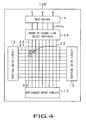
- FIG. 4 is a block circuit diagram showing display panel module that the display panel drive system has.
- FIG. 5 is a block circuit diagram showing display panel module that the display panel drive system has.
- FIG. 6 is a view showing ratio between write time of video signal by the conventional system and write time which can be ensured in the above-mentioned display panel drive system.
- FIG. 7 is a view showing the number of switches SWN necessary for respective display formats.
- FIG. 8 is a view for explaining the number of developments of video signals by post-drive.
- FIGS. 9A to 9G are views showing, every display format, the state where video signals are developed by the post-drive.
- FIGS. 10A to 10F are views showing the state where video signals have been written into pixels by the signal line select sampling system.
- The embodiments of a drive apparatus, a drive method and a display panel drive system according to the present invention will now be explained in detail with reference to the attached drawings.
- The liquid crystal
panel drive system 1 according to the present invention will be explained by using FIG. 3. - The liquid crystal
panel drive system 1 is provided at, e.g., liquid crystal projector of three plate (panel) type, etc., and comprises, as liquid crystal panel, aliquid crystal panel 9R for red, aliquid crystal panel 9G for green and aliquid crystal panel 9G for blue. - Moreover, the liquid crystal
panel drive system 1 comprises a DSD (Digital Signal Driver) 2 for implementing a predetermined signal processing to a digital video signal delivered from the external, aPre Driver 3 for driving theliquid crystal panel 9R, aPost Driver 4, aPre Driver 5 for driving theliquid crystal panel 9G, aPost Driver 6, aPre Driver 7 for driving the liquid crystal panel 9B, and aPost Driver 8. - The
liquid crystal panel 9R and thePost Driver 4 are caused to be of the module configuration as a liquidcrystal panel module 10R along with vertical drive circuit (not shown). Similarly, theliquid crystal panel 9G and the Post-Driver 6 are caused to be of module configuration as a liquidcrystal panel module 10G along with vertical drive circuit (not shown). The liquid crystal panel 9B and thePost Driver 8 are caused to be of the module configuration as a liquidcrystal panel module 10B along with vertical drive circuits (not shown). - The
DSD 2 comprises a DSD core 2a, a memory 2b, and a TG (Timing Generator) 2c. - The DSD core 2a serves to implement digital signal processing such as gamma correction and/or color unevenness correction, etc. to respective digital video signals of RGB delivered from the external. Respective digital video signals of RGB are delivered from the external as parallel data of 12 bits. The numeric value of the 12 bits is based on the fact that video signal is handled by 12 bits in the liquid crystal
panel drive system 50 shown as the prior art, and is a value only diverted (used) from a viewpoint of design. Accordingly, it is not necessarily required that this value is 12 bits, and takes m (m is natural number) bits. - In the memory 2b, there are stored respective digital video signals of RGB which have been caused to undergo digital signal processing at the DSD core 2a. The respective digital video signals of RGB stored in the memory 2b are converted into data arrangement corresponding to display format such as SVGA, XGA, WXGA, SXGA, SXGA+, UXGA, or Full HD, and are respectively delivered to
Pre Drivers Pre Driver 3 is supplied, in parallel, with digital video signals R1, R2 of 12 bits. ThePre Driver 5 is supplied, in parallel, with digital video signal of 12 bits as digital video signals G1, G2. ThePre Driver 7 is supplied, in parallel, with digital video signal of 12 bits as digital video signals B1, B2. - The timing generator 2c that the
DSD 2 has generates timing pulse S2 delivered to thePre Drivers timing pulse S 1 delivered to the liquidcrystal panel modules Pre Drivers crystal panel modules timing pulse S 1 or S2. - The
Pre Drivers DSD 2 into analog video signal of p (p is natural number-phase on the basis of the timing pulse S2 synchronous with video signal to respectively deliver those video signals to thePost Drivers Pre Drivers Pre Drivers DSD 2 into analog video signal of p = 12 phase. - Moreover, the
Pre Drivers liquid crystal panels - Then, the liquid
crystal panel modules crystal panel modules liquid crystal panels crystal panel modules liquid crystal panel 10R will be explained as representative. - As shown in FIG. 4, the liquid
crystal panel module 10R comprisesPost Driver 4,liquid crystal panel 9R, avertical drive circuit 12, a pre-charge drive circuit, and a group of signal line select switches 14. - The
Post Driver 4 respectively develops analog video signals of 12 phase delivered from thePre Driver 3 into video signals corresponding to the number of outputs which comply with display formats such as SVGA, XGA, WXGA, SXGA, SXGA+, UXGA, and/or Full HD on the basis oftiming pulse S 1 synchronous with video signal to deliver the video signals thus developed to theliquid crystal panel 9R through video signal supply line VSIGN (N is natural number) and the group of signal line select switches 14. - The development processing from the analog signals of 12 phase at the
Post Driver 4 into video signals corresponding to the number of outputs which comply with the above-described display format is processing based on the sampling system executed in the liquid crystalpanel drive system 1. - The sampling system of the liquid crystal
panel drive system 1 is a system of first selecting signal line which will be described later that theliquid crystal panel 9R has by the number of outputs of video signals which have been developed at thePost Driver 4 to subsequently perform, plural times, an operation to write, at a time, at the same timing, video signals developed with respect to selected signal lines to perform sampling with respect to all signal lines. This sampling system is called signal line select sampling system. - The number of video signals developed by the
Post Driver 4 on the basis of the signal line select sampling system is relatively determined by the display format of theliquid crystal panel 9R and the number of write operations for writing video signals onto all signal lines of theliquid crystal panel 9R. - For example, when the display format of the
liquid crystal panel 9R is high definition display format having large number of pixels, it is necessary to increase the number of developments of video signals. Moreover, when the number of times required for writing video signals onto all signal lines of theliquid crystal panel 9R is decreased, it is required to increase signal lines onto which video signals are to be written at a time. Accordingly, it is necessary to also increase the number of developments of video signals. The signal line select sampling system will be explained in detail later. - The
liquid crystal panel 9R comprisesplural gate lines 21 wired in a row form,plural signal lines 22 wired in a column form, andpixels 23 disposed at portions where both lines intersect with each other. - The
pixel 23 is composed of Thin Film Transistor (TFT) which is not shown, and liquid crystal cell which is not similarly shown. The gate electrode of the TFT is connected to correspondinggate line 21, the source electrode thereof is connected tocorresponding signal line 22, and the drain electrode thereof is connected to one electrode (pixel electrode) of corresponding liquid crystal cell. The other electrode (opposite electrode) of the liquid crystal cell is supplied with panel common DC voltage (VCOM) generated at thePre Driver 3 as a predetermined opposite potential. - The
vertical drive circuit 12 is divided into left and right portions, which are connected to the gate lines 21, and serves to linearly sequentially drive the connectedrespective gate lines 21 from the both sides thus to selectpixels 23 in a row direction. - The
pre-charge drive circuit 13 applies, in advance, prior to write operation of video signal, pre-charge signal (PSIG) delivered from thePre Driver 3 through pre-charge line (not shown) torespective signal lines 22 to perform pre-charge operation. This pre-charge operation is performed prior to write operation of video signals with respect torespective pixels 23. - A group of signal line
select switches 14 is each comprised of plural switches for performing sampling of video signals delivered from thePost Driver 4 through video signal supply line VSIGN with respect to thesignal line 22. The plural switches that the group of signal lineselect switches 14 are switched at the same timing on the basis of timing pulse S1 delivered from TG2c of the DSD2 to repeat such switching operations plural times to thereby perform sampling of video signals with respect to allsignal lines 22 that theliquid crystal panel 9R has. The video signals which have been caused to undergo sampling with respect to thesignal line 22 are written intopixels 23 in the row direction selected by thevertical drive circuit 12. - Subsequently, the configuration of the liquid crystal panel module required in carrying out the signal line select sampling system will be described in detail by using the liquid
crystal panel module 10R with reference to FIG. 5. - As shown in FIG. 5, N (N is natural number) number of video signal supply lines VSIG1 to VSIGN connected to the
Post Driver 4 are respectively connected to thesignal lines 22 through switches SWN that the group of signal lineselect switches 14 have. The switches SWN are provided, one by one, at sixsignal lines 22 adjacent in the state where they do not overlap with each other among the signal lines 22, and serve to selectsingle signal line 22 every time timing pulse S1 is delivered from the group of signal lines with the sixsignal lines 22 being as unit. - For example, at the switch SW1,
signal line 22 located at the left end of the group of signal lines is selected at timing by the first timing pulse S1. and signal line adjacent at the right side is selected at the subsequent timing Thus, the remaining foursignal lines 22 are selected in sequence. Similarly, at the switch SWN except for the switch SW1,signal lines 22 are selected at the same timing as that of the switch SW1 in order from the left end of the group of six signal lines. - As described above, respective switches SWN are simultaneously operated by timing pulse S1 to select respective one signal lines 22. Accordingly, the number of write operations with respect to all
signal lines 22 that theliquid crystal panel 9R has becomes equal to the number of selections of thesignal lines 22 by the switch SWN, i.e., six times here. - The switches SWN may be provided in units of six signal lines as described above with respect to the
signal lines 22 that theliquid crystal panel 9R has, and may be provided in units of arbitrary number of signal lines, e.g., in units of four signal lines or in units of eight signal lines. According as the number ofsignal lines 22 to be selected by the switch SWN is reduced and the number of switches SWN installed or provided is increased, the number ofsignal lines 22 which can be subject to sampling at a time becomes large. For this reason, it becomes possible to sufficiently ensure write time with respect to thesignal line 22. - Ratios of write time A which can be ensured in the signal line select sampling system of the conventional system with respect to write time B by the plural pixel simultaneous sampling system (write time required in the case where six pixels are caused to undergo simultaneous sampling) are respectively shown in the case where the number of
signal lines 22 to be selected is set to 1, 2 , 4, 6, 8 are shown in FIG. 6. - As shown in FIG. 6, it can be understood that, in the signal line select sampling system, according as the number of signal lines to be selected by the switch SWN becomes smaller, longer write time can be ensured as compared to the conventional system.
- If the
liquid crystal panel 9R has the same display format, the number N of switches SWN constituting the group of signal lineselect switches 14 is determined by the number ofsignal lines 22 to be selected. For example, if the number ofsignal lines 22 to be selected becomes small, required number of switches SWN is increased. If the number ofsignal lines 22 to be selected becomes large, required number of switches SWN is decreased. - Moreover, if the number of
signal lines 22 to be selected is the same, the number of switches SWN is determined by the display format of theliquid crystal panel 9R. For example, when the number of selectedsignal lines 22 is set to six, the number of pixels in the row direction becomes equal to 1386 at theliquid crystal panel 9R in which the display format is WXGA. From this fact, the number ofsignal lines 22 also becomes equal to 1386. Thus, from the relationship expressed as 1386/6 = 231, 231 switches SWN are required. Similarly, in the case where the number ofsignal lines 22 to be selected is set to six and the display format is caused to be Full HD, there results 1920/6 = 320. Thus, 320 switches SWN are required. The number of switches SWN necessary every display format in the case where the number ofsignal lines 22 to be selected is fixed to six is shown in FIG. 7. In FIG. 6, "A" indicates write time by the conventional system, and "B" indicates write time by the signal line selection system. - Meanwhile, as shown in FIG. 7, in the case where the display formats of the
liquid crystal panel 9R are SVGA, XGA, SXGA, SXGA+, and UXGA, the respective numbers ofsignal lines 22 cannot be divided in the case where the number ofsignal lines 22 to be selected by the switch SWN is set to six. - Accordingly, when the number of signal lines is less than six,
signal line 22 in which the number of switches SWN to be selected is less than six would take place. However, one switch SWN is assigned also with respect to thesignal line 22. For example, since there results 800/6 = 133.33 ... in the SVGA, the number of required switches SWN is set to 134 to cope with such situation. - At this time,
dummy signal line 22 and dummy pixel are added to theliquid crystal panel 9R in order to comply with one switch SW<SUB>134 </SUB> which has been increased. In the SVGA, 133x6=798signal lines 22 are caused to comply therewith up to the switches SW1 to SW133. Since six signal lines are supplemented by the switch SW134, 804signal lines 22 are necessary. In the display format of SVGA, since 800signal lines 22 exist, fourdummy signal lines 22 are newly required. In view of the above, only four dummy pixel number (D) is also added by four in the row direction in correspondence with fourdummy signal lines 22 to be newly supplemented. The number of horizontal pixels shown in FIG. 7 is the number of horizontal pixels (Ha) in which dummy pixel number (D) is taken into consideration. In FIG. 7, "*" indicates that no dummy pixel is required. - Also in regard to other display formats XGA, SXGA, SXGA+ and UXGA,
dummy signal lines 22 and dummy pixels are supplemented to theliquid crystal panel 9R in entirely the same manner to allow the number of horizontal pixels to be the number of horizontal pixels (Ha) as shown in FIG. 7, thereby making it possibly to take matching with the number of switches SWN. - Subsequently, video signal delivered from the
Post Driver 4 to the switch SWN through video signal supply lines VSIG1 to VSIGN will be explained. The video signal delivered from thePost Driver 4 to the switch SWN through video signal supply lines VSIG1 to VSIGN is a video signal developed from analog video signals of 12-phase at thePost Driver 4. - As described above, in the signal line select sampling system carried out in the liquid crystal
panel drive system 1 according to the present invention, sampling of video signal is performed by switching operation by the switch SWN with respect to thesignal line 22 of theliquid crystal panel 9R. - Accordingly, video signals delivered from the
Post Driver 4 through video signal supply lines VSIG1 to VSIGN are also required by the number of switches SWN. - In view of the above, the
Post Driver 4 develops video signals of 12-phase delivered from thePre Driver 3 by the number of switches SWN determined by the display format of theliquid crystal panel 9R and the number of write operations with respect to thesignal line 22 that theliquid crystal panel 9R has to output the video signals thus developed. - The number of outputs, i.e., the number of developments of video signals from the
Post Driver 4 every display formats such as SVGA, XGA, WXGA, SXGA, SXGA+, UXGA, Full HD in the case where the number ofsignal lines 22 to be selected by the switch SWN is set to six is shown in FIG. 8. As stated above, the number of developments of video signals from thePost Driver 4 is determined by the display format of theliquid crystal panel 9R and the number ofsignal lines 22 to be selected by the switch SWN. - From this fact, when the number of
signal lines 22 of theliquid crystal panel 9R is set to x and the number of selectedsignal lines 22 per one switch SWN is set to k, switches SWN are required with respect to respective groups of x/k number of signal lines consisting of k number of signal lines adjacent in the state where they do not overlap with each other. For this reason, the number of developments by thePost Driver 4 also results in x/k phase. - Moreover, the total number of developments shown in FIG. 8 indicates the number of developments per one phase of analog video signals of p-phase delivered from the
Pre Driver 3 to thePost Driver 4. For example, when p is set to 12, thePost Driver 4 respectively develops analog video signals of 12-phase into analog video signals of 27-phase as shown in FIG. 9A in the Full HD. - At this time, the number of video signals developed into video signals of 27-phase becomes equal to 12×27=324 in total. Since the number of outputs by the
Post Driver 4 becomes equal to 320 from the number of switches SWN necessary in the case where the display format is Full HD and the number of selectedsignal line 22 is six, four video signals are delivered to the dummy terminal, etc. so that they are not outputted. 320 video signals except for the above are delivered to 320 video signal supply lines VSIG1, to VSIG320 connected to thePost Driver 4. - Similarly, in the case where the display format of the
liquid crystal panel 9R is UXGA, SXGA+, SXGA, WXGA, XGA, SVGA, thePost Driver 4 develops the video signals of 12-phase by the total number of developments shown in FIG. 8 to output the video signals thus developed to video signal supply lines VSIG1 to VSIGN in a manner such that they are thinned as shown in FIGS. 9B, 9C, 9D, 9E, 9F, 9G. - Accordingly, in the liquid
crystal drive system 1, the number of outputs pins of thePost Driver 4 of the liquidcrystal panel module 9R, the number of video signal supply lines VSIGN physically wired and the number of switches SW<SUB>N</SUB> prepared at the group of signal lineselect switches 14 are designed so as to comply with the highest definition display format, e.g., Full HD to thereby adjust the number of developments of analog video signals of p-phase delivered from thePre Driver 3 by thePost Driver 4 even in the case where liquid crystal panel of any display format is used thus to have ability to flexibly cope with such situation only by simple adjustment to suitably change timing pulse, etc. by the DSD2. - Further, the video signal which has been developed at the
Post Driver 4 and has been delivered to video signal supply lines VSIG1 to VSIGN is delivered to respective switches SWN that the group of signal lineselect switches 14 has. The video signal thus obtained is delivered to thesignal line 22 that each switch SWN selects every time timing pulse S1 is delivered, and is written intopixels 23 on thegate line 21 selected by thevertical drive circuit 12. - For example, assuming that the number of
signal lines 22 to be selected by the switch SWN is six, video signals are simultaneously written with respect to pixels arranged at interval of five pixels from pixel of the left end as shown in FIG. 10A at a first timing, and video signals are sequentially written into pixel adjacent at the right side as shown in FIGS. 10B, 10C, 10D, 10E, 10F at the subsequent timings. - In this case, the region of cross lines indicated at a in FIG. 10 indicates pixel which has been already written, and the region of slanting lines indicated at b indicates pixel which has been newly written.
- Accordingly, in the signal line select sampling system, since pixels to be written at the same timing are not adjacent to each other so that they maintain a predetermined pixel spacing, there is no possibility that even in the case where the phase relationship between video signal and timing pulse deviates, this affects other pixels. Namely, it is possible to completely remove occurrence cause of ghost taking place resulting from the fact that, as in the case of the plural pixel simultaneous sampling system, in the case where phase relationship between video signal and timing pulse deviates, video signal is inserted (written) also except for video signals which are primarily to be written.
- While explanation has been given in the above-described explanation by using the
Pre Driver 3, thePost Driver 4 and theliquid crystal panel 9R, the signal line select sampling system is executed in entirely the same manner also in the case of theliquid crystal panel 9G driven by thePre Driver 5 and thePost Driver 6 and/or the liquid crystal panel 9B driven by thePre Driver 7 and thePost Driver 8. - As stated above, in the signal line select sampling system executed by the liquid crystal
panel drive system 1, since the number of pixels which can be written at a time is greatly increased to a degree, e.g., from six to 100 pixels or more as compared to the plural simultaneous sampling system carried out as the prior art, it is possible to ensure write time which is larger than two times or more. For this reason, stable write operation is performed. - In addition, it is possible to comply with liquid crystal panels of various display formats by the same system configuration without performing change of IC, etc. Particularly, in SXGA+, UXGA, Full HD of high resolution, it becomes possible to greatly simplify the system configuration.
- It is to be noted that while the present invention has been described in accordance with preferred embodiments thereof in the accompanying drawings and described in detail, it should be understood by those ordinarily skilled in the art that the invention is not limited to embodiments, but various modifications, alternative constructions or equivalents can be implemented without departing from the scope and spirit of the present invention as set forth by appended claims.
Claims (5)
- A drive apparatus adapted for driving a display panel having x × y number of pixels arranged in a matrix form at intersecting portions of x (x is natural number) number of signal lines disposed in a column direction and y (y is natural number) number of gate lines disposed in a row direction,
the drive apparatus comprising:
data arrangement converting means for converting a digital video signal of m (m is natural number) bits into data arrangement in conformity with display format of the display panel;
first signal processing means for converting the digital video signal of the m bits which has been converted into the data arrangement in conformity with the display format by the data arrangement converting means into parallel analog video signals of p (p is natural number)-phase;
second signal processing means for developing the analog video signals of the p-phase which have been converted by the first signal processing means into analog video signals of x/k (k is natural number)-phase to deliver the analog video signals thus developed to the x/k number of video signal supply lines which have been selected from N (N is natural number which satisfies N≥(x/k)) number of video signal supply lines; and
signal line selecting means for sequentially selecting, one by one, at the same timing, desired signal lines from respective groups of the x/k number of signal lines obtained by dividing the x number of signal lines into the k number of the signal lines adjacent in the state where they do not overlap with each other to perform sampling of the analog video signals delivered via the x/k number of video signal supply lines with respect to the selected signal lines,
wherein x, y, p, m, k are natural numbers and N is natural number which satisfies N≥(x/k). - The drive apparatus as set forth in claim 1,
wherein the display panel that the drive apparatus drives includes a dummy signal line or lines, in addition to a signal line or lines determined by the display format of the display panel so that the number x of signal lines of the display panel becomes equal to multiple of the k, and further includes a dummy pixel or pixels corresponding to the dummy signal line or lines. - A drive method of driving a display panel having x × y number of pixels arranged in a matrix form at intersecting portions of x number of signal lines disposed in a column direction and y number of gate lines disposed in a row direction,
the drive method comprising:
converting a digital video signal of m bits into data arrangement in conformity with display format of the display panel;
converting the digital video signal of the m bits which has been converted into the data arrangement in conformity with the display format into parallel analog video signals of p-phase;
developing the analog video signals of the p-phase into analog video signals of x/k-phase to deliver the analog video signal thus developed to the x/k number of video signal supply lines which have been selected from N number of video signal supply lines;
sequentially selecting, one by one, at the same timing, desired signal lines from respective groups of the x/k number of signal lines obtained by dividing the x number of signal lines into the k number of signal lines adjacent in the state where that they do not overlap with each other; and
performing sampling of the analog video signals delivered via the x/k number of video signal supply lines with respect to the selected signal lines,
wherein x, y, p, m, k are natural numbers, and N is natural number which satisfies N≥(x/k). - A display panel drive system of driving a display panel having x × y number of pixels arranged in a matrix form at intersecting portions of x number of signal lines disposed in a column direction and y number of gate lines disposed in a row direction,
the display panel drive system comprising:
a data arrangement converting unit for converting a digital video signal of m bits into data arrangement in conformity with display format of the display panel;
a signal processing unit for converting the digital video signal of the m bits which has been converted into the data arrangement in conformity with the display format by the data arrangement converting unit into parallel analog video signals of p-phase; and
a display panel module including the display panel having an arbitrary display format, signal processing means for developing the analog video signals of the p-phase which have been converted by the signal processing unit into analog video signals of x/k-phase to deliver the analog video signals thus developed to N number of video signal supply lines, a vertical drive circuit connected to the gate lines and serving to linearly sequentially drive the gate lines to select the x number of pixels in the row direction, signal line selecting means for sequentially selecting, one by one, at the same timing, desired signal lines from respective groups of the x/k number of signal lines obtained by dividing the x number of signal lines into the k number of signal lines adjacent in the state where they do not overlap with each other to perform sampling of the analog video signals delivered via the x/k number of video signal supply lines with respect to the selected signal lines, and video signal writing means for writing the analog video signals which have been caused to undergo sampling at the signal lines by the signal line selecting means into the pixels in the row direction which have been selected by the vertical drive circuit,
wherein x, y, p, m, k are natural numbers, and N is natural number which satisfies N≥(x/k). - The display panel drive system as set forth in claim 4,
wherein the display panel includes a dummy signal line or lines in addition to a signal line or lines determined by display format of the display panel so that the number x of signal lines of the display panel becomes multiple of the k, and further includes a dummy pixel or pixels corresponding to the dummy signal line or lines.
Applications Claiming Priority (2)
| Application Number | Priority Date | Filing Date | Title |
|---|---|---|---|
| JP2003307921A JP4100299B2 (en) | 2003-08-29 | 2003-08-29 | Driving device, driving method, and display panel driving system |
| PCT/JP2004/012255 WO2005022503A1 (en) | 2003-08-29 | 2004-08-26 | Driving apparatus, driving method, and display panel driving system |
Publications (2)
| Publication Number | Publication Date |
|---|---|
| EP1662470A1 true EP1662470A1 (en) | 2006-05-31 |
| EP1662470A4 EP1662470A4 (en) | 2007-12-05 |
Family
ID=34269467
Family Applications (1)
| Application Number | Title | Priority Date | Filing Date |
|---|---|---|---|
| EP04772211A Ceased EP1662470A4 (en) | 2003-08-29 | 2004-08-26 | CONTROL APPARATUS AND METHOD AND DISPLAY PANEL CONTROL SYSTEM |
Country Status (7)
| Country | Link |
|---|---|
| US (1) | US7719514B2 (en) |
| EP (1) | EP1662470A4 (en) |
| JP (1) | JP4100299B2 (en) |
| KR (1) | KR101063128B1 (en) |
| CN (1) | CN100446074C (en) |
| TW (1) | TW200518024A (en) |
| WO (1) | WO2005022503A1 (en) |
Cited By (1)
| Publication number | Priority date | Publication date | Assignee | Title |
|---|---|---|---|---|
| US7768476B2 (en) | 2005-04-06 | 2010-08-03 | Lg Electronics Inc. | Plasma display apparatus and driving method thereof |
Families Citing this family (7)
| Publication number | Priority date | Publication date | Assignee | Title |
|---|---|---|---|---|
| JP4569213B2 (en) * | 2004-08-06 | 2010-10-27 | ソニー株式会社 | Display device and driving method of display device |
| JP2006202602A (en) * | 2005-01-20 | 2006-08-03 | Sugatsune Ind Co Ltd | Variable color lighting device |
| JP2009008943A (en) | 2007-06-28 | 2009-01-15 | Sony Corp | Display device |
| WO2009060656A1 (en) * | 2007-11-08 | 2009-05-14 | Sharp Kabushiki Kaisha | Data processing device, liquid crystal display, television receiver, and data processing method |
| JP2011059216A (en) * | 2009-09-08 | 2011-03-24 | Renesas Electronics Corp | Display device and display control method |
| CN104599654B (en) * | 2015-02-05 | 2016-10-19 | 京东方科技集团股份有限公司 | Chromacoder and method, signal generating system and display device |
| JP6949927B2 (en) * | 2019-12-12 | 2021-10-13 | Necプラットフォームズ株式会社 | Light transmitter, communication system, and light transmission method |
Family Cites Families (14)
| Publication number | Priority date | Publication date | Assignee | Title |
|---|---|---|---|---|
| JPS62147488A (en) | 1985-12-21 | 1987-07-01 | 株式会社日立製作所 | Drive circuit for active matrix display devices |
| US5170158A (en) * | 1989-06-30 | 1992-12-08 | Kabushiki Kaisha Toshiba | Display apparatus |
| JP2862592B2 (en) | 1989-06-30 | 1999-03-03 | 株式会社東芝 | Display device |
| EP0760508B1 (en) * | 1995-02-01 | 2005-11-09 | Seiko Epson Corporation | Liquid crystal display device, and method of its driving |
| JP3403027B2 (en) | 1996-10-18 | 2003-05-06 | キヤノン株式会社 | Video horizontal circuit |
| TW455725B (en) * | 1996-11-08 | 2001-09-21 | Seiko Epson Corp | Driver of liquid crystal panel, liquid crystal device, and electronic equipment |
| JPH10149139A (en) | 1996-11-18 | 1998-06-02 | Sony Corp | Image display device |
| JP3675113B2 (en) | 1997-06-10 | 2005-07-27 | ソニー株式会社 | Display device |
| US6693616B2 (en) * | 2000-02-18 | 2004-02-17 | Semiconductor Energy Laboratory Co., Ltd. | Image display device, method of driving thereof, and electronic equipment |
| JP2002099251A (en) | 2000-09-21 | 2002-04-05 | Victor Co Of Japan Ltd | Liquid crystal display device |
| JP2002108299A (en) | 2000-09-29 | 2002-04-10 | Sony Corp | Image display device, liquid crystal display device, and liquid crystal projector |
| KR100864917B1 (en) * | 2001-11-03 | 2008-10-22 | 엘지디스플레이 주식회사 | Data driving device and method of liquid crystal display |
| JP3730161B2 (en) * | 2001-11-28 | 2005-12-21 | シャープ株式会社 | Liquid crystal display device |
| JP4190921B2 (en) * | 2002-04-10 | 2008-12-03 | シャープ株式会社 | Driving circuit and display device including the same |
-
2003
- 2003-08-29 JP JP2003307921A patent/JP4100299B2/en not_active Expired - Lifetime
-
2004
- 2004-08-23 TW TW093125362A patent/TW200518024A/en not_active IP Right Cessation
- 2004-08-26 US US10/568,860 patent/US7719514B2/en active Active
- 2004-08-26 KR KR1020067003973A patent/KR101063128B1/en not_active Expired - Fee Related
- 2004-08-26 EP EP04772211A patent/EP1662470A4/en not_active Ceased
- 2004-08-26 CN CNB2004800249470A patent/CN100446074C/en not_active Expired - Fee Related
- 2004-08-26 WO PCT/JP2004/012255 patent/WO2005022503A1/en not_active Ceased
Cited By (1)
| Publication number | Priority date | Publication date | Assignee | Title |
|---|---|---|---|---|
| US7768476B2 (en) | 2005-04-06 | 2010-08-03 | Lg Electronics Inc. | Plasma display apparatus and driving method thereof |
Also Published As
| Publication number | Publication date |
|---|---|
| KR101063128B1 (en) | 2011-09-07 |
| TWI301262B (en) | 2008-09-21 |
| CN1846245A (en) | 2006-10-11 |
| JP2005077745A (en) | 2005-03-24 |
| CN100446074C (en) | 2008-12-24 |
| US20060262064A1 (en) | 2006-11-23 |
| TW200518024A (en) | 2005-06-01 |
| JP4100299B2 (en) | 2008-06-11 |
| US7719514B2 (en) | 2010-05-18 |
| KR20060130011A (en) | 2006-12-18 |
| WO2005022503A1 (en) | 2005-03-10 |
| EP1662470A4 (en) | 2007-12-05 |
Similar Documents
| Publication | Publication Date | Title |
|---|---|---|
| EP1191513B1 (en) | Active matrix display device | |
| US7508479B2 (en) | Liquid crystal display | |
| US5748175A (en) | LCD driving apparatus allowing for multiple aspect resolution | |
| US6542139B1 (en) | Matrix type display apparatus | |
| US8269706B2 (en) | Operating unit of liquid crystal display panel and method for operating the same | |
| US20060061535A1 (en) | Liquid crystal display device and method of driving the same | |
| JP2009058675A (en) | Display device | |
| CN100410997C (en) | Liquid crystal display device | |
| US6977634B2 (en) | Apparatus and method for driving image display device | |
| US7719514B2 (en) | Apparatus and method for converting a digital video signal to conform with a display panel format | |
| JP2004521397A (en) | Display device and driving method thereof | |
| US7538754B2 (en) | Signal circuit, display apparatus including same, and method for driving data line | |
| KR100965587B1 (en) | LCD and its driving method | |
| US6771238B1 (en) | Liquid crystal display device | |
| JPH0854601A (en) | Active matrix liquid crystal display device | |
| JP4569213B2 (en) | Display device and driving method of display device | |
| JPH10149139A (en) | Image display device | |
| JP2004309822A (en) | Display device | |
| KR20060061835A (en) | Active matrix display device | |
| JPH11296133A (en) | Drive circuit for image display device | |
| US20020067337A1 (en) | Liquid crystal display imager and clock reduction method | |
| KR101238006B1 (en) | Liquid crystal display having column-gate driver | |
| WO2015137428A1 (en) | Liquid crystal driving device and liquid crystal display device | |
| WO2004017288A2 (en) | Multi-panel liquid crystal display systems | |
| JPH11305263A (en) | Liquid crystal display device and liquid crystal panel used therefor |
Legal Events
| Date | Code | Title | Description |
|---|---|---|---|
| PUAI | Public reference made under article 153(3) epc to a published international application that has entered the european phase |
Free format text: ORIGINAL CODE: 0009012 |
|
| 17P | Request for examination filed |
Effective date: 20060227 |
|
| AK | Designated contracting states |
Kind code of ref document: A1 Designated state(s): DE FR GB |
|
| DAX | Request for extension of the european patent (deleted) | ||
| RBV | Designated contracting states (corrected) |
Designated state(s): DE FR GB |
|
| A4 | Supplementary search report drawn up and despatched |
Effective date: 20071105 |
|
| 17Q | First examination report despatched |
Effective date: 20080226 |
|
| REG | Reference to a national code |
Ref country code: DE Ref legal event code: R003 |
|
| STAA | Information on the status of an ep patent application or granted ep patent |
Free format text: STATUS: THE APPLICATION HAS BEEN REFUSED |
|
| 18R | Application refused |
Effective date: 20111104 |