EP1657659A1 - Printed circuit board return route check method and printed circuit board pattern design cad device - Google Patents
Printed circuit board return route check method and printed circuit board pattern design cad device Download PDFInfo
- Publication number
- EP1657659A1 EP1657659A1 EP05709686A EP05709686A EP1657659A1 EP 1657659 A1 EP1657659 A1 EP 1657659A1 EP 05709686 A EP05709686 A EP 05709686A EP 05709686 A EP05709686 A EP 05709686A EP 1657659 A1 EP1657659 A1 EP 1657659A1
- Authority
- EP
- European Patent Office
- Prior art keywords
- guard ground
- ground
- guard
- discriminant value
- signal wiring
- Prior art date
- Legal status (The legal status is an assumption and is not a legal conclusion. Google has not performed a legal analysis and makes no representation as to the accuracy of the status listed.)
- Granted
Links
Images




Classifications
-
- G—PHYSICS
- G06—COMPUTING OR CALCULATING; COUNTING
- G06F—ELECTRIC DIGITAL DATA PROCESSING
- G06F30/00—Computer-aided design [CAD]
- G06F30/30—Circuit design
- G06F30/39—Circuit design at the physical level
- G06F30/394—Routing
-
- H—ELECTRICITY
- H05—ELECTRIC TECHNIQUES NOT OTHERWISE PROVIDED FOR
- H05K—PRINTED CIRCUITS; CASINGS OR CONSTRUCTIONAL DETAILS OF ELECTRIC APPARATUS; MANUFACTURE OF ASSEMBLAGES OF ELECTRICAL COMPONENTS
- H05K1/00—Printed circuits
- H05K1/02—Details
- H05K1/0213—Electrical arrangements not otherwise provided for
- H05K1/0216—Reduction of cross-talk, noise or electromagnetic interference
- H05K1/0218—Reduction of cross-talk, noise or electromagnetic interference by printed shielding conductors, ground planes or power plane
- H05K1/0219—Printed shielding conductors for shielding around or between signal conductors, e.g. coplanar or coaxial printed shielding conductors
-
- H—ELECTRICITY
- H05—ELECTRIC TECHNIQUES NOT OTHERWISE PROVIDED FOR
- H05K—PRINTED CIRCUITS; CASINGS OR CONSTRUCTIONAL DETAILS OF ELECTRIC APPARATUS; MANUFACTURE OF ASSEMBLAGES OF ELECTRICAL COMPONENTS
- H05K3/00—Apparatus or processes for manufacturing printed circuits
- H05K3/0005—Apparatus or processes for manufacturing printed circuits for designing circuits by computer
Definitions
- the present invention relates to wiring design of a printed board, more specifically, to a method for checking a return path of a printed board and a CAD (computer aided design) apparatus for designing patterns of a printed board, which can take an EMC (electromagnetic compatibility) countermeasure for preventing unwanted emission noise from being generating out of a printed board.
- EMC electromagnetic compatibility
- a splay portion 43 of a guard ground, around which a pad or a via hole is located for a signal wiring pattern 31, will be judged as an error of discontinuity of the guard ground.
- a short erroneous discontinued portion 44 of the guard ground will be judged all right.
- a method for checking a return path of a printed board includes steps of:
- the printed board is a multilayer printed board including a wiring layer in which the signal wiring pattern resides, and a ground layer in which a ground plane resides, and the method further includes a step of judging an error of guard ground when no guard ground exists within the distance to the second discriminant value GU in the non-guard ground section and no ground, which is connected to the guard ground, exists in the ground layer.
- the first discriminant value GL is defined as a shortest distance between lines during pattern design of the printed board.
- the above-mentioned checking method can be realized as a program executable on a computer, and the program can be recorded in a recording media.
- a CAD apparatus for designing patterns of a printed board includes:
- Fig. 1 is a block diagram showing an example of a CAD apparatus for EMC design according to the present invention.
- Fig. 2 is a flowchart showing an example of a method for checking a return path of a printed board, according to the present invention.
- Figs. 3A and 3B are partial plan views for illustrating detection of a guard ground.
- the CAD apparatus for EMC design includes an input and output device 11, such as keyboard, pointing device or display, a computer 11 for design of circuit, such as computing processor, a storage device 13, such as hard disk drive, optical disk drive or memory, and a printed board CAD program 14 for design of circuit patterns, containing a guard ground detecting means 21.
- an input and output device 11 such as keyboard, pointing device or display
- a computer 11 for design of circuit such as computing processor
- a storage device 13 such as hard disk drive, optical disk drive or memory
- a printed board CAD program 14 for design of circuit patterns, containing a guard ground detecting means 21.
- the guard ground detecting means 21 includes a signal wiring pattern detecting unit 22, a guard ground detecting unit 23, a plane ground detecting unit 24, and a return path judging unit 25.
- the signal wiring pattern detecting unit 22 detects each of signal wiring patterns with reference to wiring information of the printed board to be designed. This wiring information is stored as design data of the printed board in the storage device 13.
- the guard ground detecting unit 23 traces each of the signal wiring patterns, which are detected by the signal wiring pattern detecting unit 22, along the longitudinal direction thereof, to detect whether or not a guard ground, which functions as return path of the particular signal wiring pattern, exists on both sides of the signal wiring pattern.
- a first guard ground discriminant value GL for defining a search range is set up in advance, and existence of such a guard ground is detected within a distance from a center line of the signal wiring pattern to the first guard ground discriminant value GL.
- the guard ground detecting unit 23 identifies a section in which a guard ground exists within the distance to the first guard ground discriminant value GL, and another section in which no guard ground exists within the distance to the first guard ground discriminant value GL, to define the former as a guard ground OK section and the latter as a guard ground NG section, respectively.
- a second guard ground discriminant value GU which is larger than the first guard ground discriminant value GL, is set up in advance. Existence of the guard ground is detected within another distance from a center line of the signal wiring pattern to the second guard ground discriminant value GU.
- the return path judging unit 25 judges an error of guard ground when no guard ground exists within the distance to the second guard ground discriminant value GU in the guard ground NG section. Result of such error judgment may be represented to an operator through the input and output device 11, such as display, or be informed to another program.
- the printed board to designed is a multilayer printed board including a wiring layer in which the signal wiring pattern resides, and a ground layer in which a ground plane resides, there is a possibility that the return path of the signal wiring pattern is formed in the ground plane of the ground layer through a via hole or the like. Therefore, when the guard ground is discontinued in the wiring layer, the plane ground detecting unit 24 detects whether or not a ground, which is connected to the guard ground, exists in the ground layer.
- the signal wiring pattern detecting unit 22 detects each of signal wiring patterns with reference to wiring information of the printed board to be designed. For example, as shown in Fig. 3A, the signal wiring pattern 31 is detected.
- the first guard ground discriminant value GL is set up.
- the first guard ground discriminant value GL defines, as shown in Fig. 3A, the search range on the both sides with reference to the center line of the signal wiring pattern 31.
- the first guard ground discriminant value GL is preferably set up as a shortest distance between lines during pattern design of the printed board.
- the guard ground detecting unit 23 traces the signal wiring pattern along the longitudinal direction thereof, and then in a step a4, to detect whether or not a guard ground exists within the distance from the signal wiring pattern to the first guard ground discriminant value GL.
- the return path of the particular signal wiring pattern is meant to be secured.
- the return path judging unit 25 judges no error of guard ground to complete the return path checking routine.
- the guard ground detecting unit 23 defines the section in which the guard ground exists within the distance to the first guard ground discriminant value GL as a guard ground OK section, and the section in which no guard ground exists within the distance to the first guard ground discriminant value GL as a guard ground NG section, respectively.
- the guard ground 32 is bent so as to get away from the signal wiring pattern 31, resulting in a portion exceeding the first guard ground discriminant value GL and another portion in which the guard ground 32 is discontinued.
- the section containing these portions corresponds to a guard ground NG section 35.
- the section containing a portion which does not exceed the first guard ground discriminant value GL corresponds to a guard ground OK section.
- the second guard ground discriminant value GU is set up as larger than the first guard ground discriminant value GL.
- the second guard ground discriminant value GU is preferably set up, as shown in Fig. 3B, so as to expand more the search range in the guard ground NG section 35 and to contain the bent portion of the guard ground 32, thereby extracting only the discontinued portion of the guard ground 32.
- the second guard ground discriminant value GU may be optionally changed based on a length of the guard ground NG section. For example, in a case the first guard ground discriminant value GL is set up at 0.2 mm of the shortest distance between lines for pattern design, the second guard ground discriminant value GU may be set up at approximately 10 mm.
- the guard ground detecting unit 23 re-traces it in a range of the guard ground NG section to detect whether or not the guard ground exists within the distance to the second guard ground discriminant value GU.
- the return path judging unit 25 judges an error of guard ground, and then displaying it for an operator by means of the input and output device 11 to complete the return path checking routine.
- step a13 when the guard ground exists within the distance to the second guard ground discriminant value GU in the guard ground NG section, transferring to a step a14, it is detected whether the guard ground is continuous or not in the guard ground NG section.
- the return path of the particular signal wiring pattern is meant to be secured. Transferring to the step a5, the return path judging unit 25 judges no error of guard ground to complete the return path checking routine.
- the return path judging unit 25 judges an error of guard ground, and then displaying it for an operator by means of the input and output device 11 to complete the return path checking routine.
- the guard ground 32 is continuous without discontinuity and does not exceed the second guard ground discriminant value GU in the guard ground NG section A 35a, resulting in judgment of no error of guard ground.
- the guard ground 32 does not exist in the guard ground NG section B 35b, resulting in judgment of an error of guard ground.
- the first embodiment exemplifies a case where the second guard ground discriminant value GU is set up based on a length of the guard ground NG section.
- the second guard ground discriminant value GU may be set up based on a signal frequency or a signal current flowing in the signal wiring pattern, resulting in a similar effect.
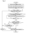
- Fig. 4 is a flowchart showing another example of a method for checking a return path of a printed board, according to the present invention.
- Fig. 5 is a partial plan view for illustrating detection of a guard ground.
- the CAD apparatus for EMC design shown in Fig. 1 is also used.
- the signal wiring pattern detecting unit 22 detects each of signal wiring patterns with reference to wiring information of the printed board to be designed. For example, as shown in Fig. 5A, the signal wiring pattern 31 is detected.
- the first guard ground discriminant value GL is set up.
- the first guard ground discriminant value GL defines, as shown in Fig. 3A, the search range on the both sides with reference to the center line of the signal wiring pattern 31.
- the first guard ground discriminant value GL is preferably set up as a shortest distance between lines during pattern design of the printed board.
- the guard ground detecting unit 23 traces the signal wiring pattern along the longitudinal direction thereof, and then in a step b4, to detect whether or not a guard ground exists within the distance from the signal wiring pattern to the first guard ground discriminant value GL.
- the return path of the particular signal wiring pattern is meant to be secured.
- the return path judging unit 25 judges no error of guard ground to complete the return path checking routine.
- the guard ground detecting unit 23 defines the section in which the guard ground exists within the distance to the first guard ground discriminant value GL as a guard ground OK section, and the section in which no guard ground exists within the distance to the first guard ground discriminant value GL as a guard ground NG section, respectively.
- the guard ground 32 is bent so as to get away from the signal wiring pattern 31, resulting in a portion exceeding the first guard ground discriminant value GL and another portion in which the guard ground 32 is discontinued.
- the section containing these portions corresponds to a guard ground NG section 35.
- the section containing a portion which does not exceed the first guard ground discriminant value GL corresponds to a guard ground OK section.
- the second guard ground discriminant value GU is set up as larger than the first guard ground discriminant value GL.
- the second guard ground discriminant value GU is preferably set up, as shown in Fig. 3B, so as to expand more the search range in the guard ground NG section 35 and to contain the bent portion of the guard ground 32, thereby extracting only the discontinued portion of the guard ground 32.
- the second guard ground discriminant value GU may be optionally changed based on a length of the guard ground NG section. For example, in a case the first guard ground discriminant value GL is set up at 0.2 mm of the shortest distance between lines for pattern design, the second guard ground discriminant value GU may be set up at approximately 10 mm.
- the guard ground detecting unit 23 re-traces it in a range of the guard ground NG section to detect whether or not the guard ground exists within the distance to the second guard ground discriminant value GU.
- the return path judging unit 25 judges an error of guard ground, and then displaying it for an operator by means of the input and output device 11 to complete the return path checking routine.
- step b13 when the guard ground exists within the distance to the second guard ground discriminant value GU in the guard ground NG section, transferring to the step b14, as shown in Fig. 5, it is judged whether or not a relation: L ⁇ 2(GU 2 -G 2 ) 1/2 is satisfied, wherein L is a length of the guard ground NG section, and G is a distance from the signal wiring pattern on the border of the guard ground NG section to the guard ground.
- the return path judging unit 25 judges an error of guard ground, and then displaying it for an operator by means of the input and output device 11 to complete the return path checking routine.
- step b14 when L > 2(GU 2 -G 2 ) 1/2 is satisfied, transferring to the step b5, the return path judging unit 25 judges no error of guard ground to complete the return path checking routine.
- Fig. 5 illustrates a case where the guard ground 32 is discontinued at guard ground terminals X 36a and Y 36b.
- a discontinuous length L thereof is equal to 2(GU 2- G 2 ) 1/2
- the terminals X and Y resides on a semicircle with a radius of GU and a center of intersection of the signal wiring pattern 31 and a center line 37 between the terminals X and Y.
- L > 2(GU 2 -G 2 ) 1/2 is satisfied, the terminals X and Y exist outside of the semicircle with the radius of GU. Therefore, the guard ground is discontinuous, resulting in an error of guard ground.
- both employment of the two larger and smaller guard ground discriminant values GL and GU, and numerical comparison of the length L of the guard ground NG section with the distance G from the signal wiring pattern on the border of the guard ground NG section to the guard ground facilitate reliable checking of the return path of the signal wiring pattern.
- Fig. 6 is a flowchart showing a third example of a method for checking a return path of a printed board, according to the present invention.
- Fig. 7 is a schematic perspective view for illustrating detection of a guard ground.
- the CAD apparatus for EMC design shown in Fig. 1 is also used.
- the printed board to designed is a multilayer printed board including a wiring layer in which the signal wiring pattern resides, and a ground layer in which a ground plane resides, there is a possibility that the return path of the signal wiring pattern is formed in the ground plane of the ground layer through a via hole or the like.
- the plane ground detecting unit 24 detects whether or not the ground which is connected with the guard ground exists in the ground layer.
- the signal wiring pattern detecting unit 22 detects each of signal wiring patterns with reference to wiring information of the printed board to be designed. For example, as shown in Fig. 7, the signal wiring pattern 31, which is connected between two ICs 38, is detected.
- the first guard ground discriminant value GL is set up.
- the first guard ground discriminant value GL defines, as shown in Fig. 3A, the search range on the both sides with reference to the center line of the signal wiring pattern 31.
- the first guard ground discriminant value GL is preferably set up as a shortest distance between lines during pattern design of the printed board.
- a plane ground discriminant value GPG is set up.
- the plane ground discriminant value GPG defines, as shown in Fig. 7, a search range in a lamination direction of the multilayer board with reference to the wiring layer 51 in which the signal wiring pattern 31 exists, for example, in terms of either an identification symbol of a layer to be searched or a distance from the wiring layer 51.
- the plane ground detecting unit 24 extracts a plane ground which exists in a range from the wiring layer, in which the particular signal wiring pattern resides, to the plane ground discriminant value GPG.
- the guard ground detecting unit 23 traces the signal wiring pattern along the longitudinal direction thereof, and then in a step c6, to detect whether or not a guard ground exists within the distance from the signal wiring pattern to the first guard ground discriminant value GL.
- the return path of the particular signal wiring pattern is meant to be secured.
- the return path judging unit 25 judges no error of guard ground to complete the return path checking routine.
- the guard ground detecting unit 23 defines the section in which the guard ground exists within the distance to the first guard ground discriminant value GL as a guard ground OK section, and the section in which no guard ground exists within the distance to the first guard ground discriminant value GL as a guard ground NG section, respectively.
- the guard ground 32 is bent so as to get away from the signal wiring pattern 31, resulting in a portion exceeding the first guard ground discriminant value GL and another portion in which the guard ground 32 is discontinued.
- the section containing these portions corresponds to a guard ground NG section 35.
- the section containing a portion which does not exceed the first guard ground discriminant value GL corresponds to a guard ground OK section.
- the second guard ground discriminant value GU is set up as larger than the first guard ground discriminant value GL.
- the second guard ground discriminant value GU is preferably set up, as shown in Fig. 3B, so as to expand more the search range in the guard ground NG section 35 and to contain the bent portion of the guard ground 32, thereby extracting only the discontinued portion of the guard ground 32.
- the second guard ground discriminant value GU may be optionally changed based on a length of the guard ground NG section. For example, in a case the first guard ground discriminant value GL is set up at 0.2 mm of the shortest distance between lines for pattern design, the second guard ground discriminant value GU may be set up at approximately 10 mm.
- the guard ground detecting unit 23 re-traces it in a range of the guard ground NG section to detect whether or not the guard ground exists within the distance to the second guard ground discriminant value GU.
- the process is transferred to a step c15.
- step c13 when the guard ground exists within the distance to the second guard ground discriminant value GU in the guard ground NG section, transferring to a step c14, it is judged whether or not the guard ground is continuous in the guard ground NG section.
- the return path of the particular signal wiring pattern is meant to be secured. Transferring to a step c7, the return path judging unit 25 judges no error of guard ground to complete the return path checking routine.
- step c14 when the guard ground is discontinuous in the guard ground NG section, the return path of the particular signal wiring pattern is meant to be lost.
- the process is transferred to the step c15.
- the plane ground detecting unit 24 searches for a plane ground extracted in the step c4 to detect whether or not the plane ground which is connected with the guard ground exists in the ground layer.
- the return path of the particular signal wiring pattern is meant to be secured.
- the return path judging unit 25 judges no error of guard ground to complete the return path checking routine.
- the guard ground 32 is discontinuous in the wiring layer 51, but is connected through a via hole 41 to an adjacent plane ground 40 in the ground layer 52, which resides within the plane ground discriminant value GPG. Therefore, the return path is secured, resulting in judgment of no error of guard ground.
- step c15 when no plane ground which is connected with the guard ground exists, transferring to a step c16, the return path judging unit 25 judges an error of guard ground, and then displaying it for an operator by means of the input and output device 11 to complete the return path checking routine.
- both employment of the two larger and smaller guard ground discriminant values GL and GU, and judgment of continuity of the guard ground by taking account of the plane ground residing in another layer facilitate reliable checking of the return path of the signal wiring pattern.
Landscapes
- Engineering & Computer Science (AREA)
- Computer Hardware Design (AREA)
- Physics & Mathematics (AREA)
- Theoretical Computer Science (AREA)
- Computer Networks & Wireless Communication (AREA)
- Evolutionary Computation (AREA)
- Geometry (AREA)
- General Engineering & Computer Science (AREA)
- General Physics & Mathematics (AREA)
- Structure Of Printed Boards (AREA)
- Production Of Multi-Layered Print Wiring Board (AREA)
Abstract
Description
- The present invention relates to wiring design of a printed board, more specifically, to a method for checking a return path of a printed board and a CAD (computer aided design) apparatus for designing patterns of a printed board, which can take an EMC (electromagnetic compatibility) countermeasure for preventing unwanted emission noise from being generating out of a printed board.
- In order to reduce unwanted emission noise from electronics, such as digital audio-visual equipment or information equipment, it is important to figure out a wiring path in a circuit board which may constitute a noise source. In a conventional CAD for a printed board, when detecting a wiring error, a person visually checked whether a wiring path of clock wiring pattern violates EMC design condition to correct the violated point of the wiring path.
- However, in the above-mentioned CAD for a printed board, since detection of error in EMC design depends on a person, there is a problem that leakage of detection is likely to occur and it takes much time to detect a error.
- For this countermeasure, since recognition technology of pattern shapes is developed in CAD for a printed board, it is possible to detect a guard ground, that is a guard pattern with ground attribution, existing adjacent to a signal wiring. For a typical detection method, if there is a wiring section in which a guard ground does not exist within a defined guard ground discriminant value with respect to a signal wiring, an error is thought to occur.
- A related prior art will be listed as follow.
- [PATENT DOCUMENT 1] JP-2002-16337-A
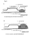
- However, in the above-mentioned method for detecting a guard ground, as shown in Fig. 8, in a case of using a small defined guard ground discriminant value G, a splay portion 43 of a guard ground, around which a pad or a via hole is located for a
signal wiring pattern 31, will be judged as an error of discontinuity of the guard ground. In another case of using a large defined guard ground discriminant value G, on the other hand, a short erroneous discontinued portion 44 of the guard ground will be judged all right. - To solve the above problem, it is an object of the present invention to provide a method for checking a return path of a printed board and a CAD apparatus for designing patterns of a printed board, which can check a return path without mistake more quickly than the conventional method.
- To attain the above object, a method for checking a return path of a printed board, according to the present invention, includes steps of:
- detecting a signal wiring pattern with reference to wiring information of the printed board;
- tracing the signal wiring pattern along the longitudinal direction thereof, to detect whether or not a guard ground exists within a distance from the signal wiring pattern to a predetermined first discriminant value GL;
- identifying a non-guard ground section in which no guard ground exists within the distance to the first discriminant value GL;
- setting up a second discriminant value GU larger than the first discriminant value GL;
- detecting whether or not a guard ground exists within another distance from the signal wiring pattern to the second discriminant value GU in the non-guard ground section; and
- judging an error of guard ground when no guard ground exists within the distance to the second discriminant value GU in the non-guard ground section.
- It is preferable in the checking method according to the present invention to include a step of judging an error of guard ground when a discontinued guard ground exists within the distance to the second discriminant value GU in the non-guard ground section.
- It is preferable in the checking method according to the present invention to include a step of judging an error of guard ground when satisfying a relation: L ≤ 2(GU2-G2)1/2 wherein L is a length of the non-guard ground section, and G is a distance from the signal wiring pattern on the border of the non-guard ground section to the guard ground.
- It is preferable in the checking method according to the present invention that the printed board is a multilayer printed board including a wiring layer in which the signal wiring pattern resides, and a ground layer in which a ground plane resides, and the method further includes a step of judging an error of guard ground when no guard ground exists within the distance to the second discriminant value GU in the non-guard ground section and no ground, which is connected to the guard ground, exists in the ground layer.
- It is preferable in the checking method according to the present invention that the first discriminant value GL is defined as a shortest distance between lines during pattern design of the printed board.
- The above-mentioned checking method can be realized as a program executable on a computer, and the program can be recorded in a recording media.
- Moreover, a CAD apparatus for designing patterns of a printed board, according to the present invention, includes:
- a signal wiring pattern detecting unit for detecting a signal wiring pattern with reference to wiring information of the printed board;
- a guard ground detecting unit for tracing the signal wiring pattern along the longitudinal direction thereof, to detect whether or not a guard ground exists within a distance from the signal wiring pattern to a predetermined first discriminant value GL, and for identifying a non-guard ground section in which no guard ground exists within the distance to the first discriminant value GL, and for detecting whether or not a guard ground exists within another distance from the signal wiring pattern to a second discriminant value GU, which is larger than the first discriminant value GL, in the non-guard ground section; and
- a return path judging unit for judging an error of guard ground when no guard ground exists within the distance to the second discriminant value GU in the non-guard ground section.
- According to this approach, it is possible to check quickly both of a splay portion and a short discontinued portion of the guard ground without mistake. Consequently, an EMC countermeasure for suppressing an electromagnetic wave generated from a high frequency current loop, which is configured of the signal wiring and the guard ground, can be effectively adopted.
-
- Fig. 1 is a block diagram showing an example of a CAD apparatus for EMC design according to the present invention.
- Fig. 2 is a flowchart showing an example of a method for checking a return path of a printed board, according to the present invention.
- Figs. 3A and 3B are partial plan views for illustrating detection of a guard ground.
- Fig. 4 is a flowchart showing another example of a method for checking a return path of a printed board, according to the present invention.
- Fig. 5 is a partial plan view for illustrating detection of a guard ground.
- Fig. 6 is a flowchart showing a third example of a method for checking a return path of a printed board, according to the present invention.
- Fig. 7 is a schematic perspective view for illustrating detection of a guard ground.
- Fig. 8 is a partial plan view for illustrating a conventional method for detecting a guard ground.
-
- 11: INPUT AND OUTPUT DEVICE
- 12: COMPUTER FOR DESIGN OF CIRCUIT PATTERNS
- 13: STORAGE DEVICE
- 14: PRINTED BOARD CAD PROGRAM FOR DESIGN OF CIRCUIT PATTERNS
- 21: GUARD GROUND DETECTING MEANS
- 22: SIGNAL WIRING PATTERN DETECTING UNIT
- 23: GUARD GROUND DETECTING UNIT
- 24: PLANE GROUND DETECTING UNIT
- 25: RETURN PATH JUDGING UNIT
- 31: SIGNAL WIRING PATTERN
- 32: GUARD GROUND
- 34: GUARD GROUND OK SECTION
- 35: GUARD GROUND NG SECTION
- 35a: GUARD GROUND NG SECTION A
- 35b: GUARD GROUND NG SECTION B
- 36a: GUARD GROUND TERMINAL X
- 36b: GUARD GROUND TERMINAL Y
- 37: CENTER LINE BETWEEN X AND Y
- 38: IC
- 39: GROUND PLANE
- 40: ADJACENT GROUND PLANE
- 41: VIA HOLE
- 42: RETURN PATH
- 43: SPLAY PORTION OF GUARD GROUND
- 44: DISCONTINUED PORTION OF GUARD GROUND
- 45: SEMICIRCLE OF RADIAL DISCRIMINANT VALUE
- 51: WIRING LAYER
- 52: GROUND LAYER
- Fig. 1 is a block diagram showing an example of a CAD apparatus for EMC design according to the present invention. Fig. 2 is a flowchart showing an example of a method for checking a return path of a printed board, according to the present invention. Figs. 3A and 3B are partial plan views for illustrating detection of a guard ground.
- First, in Fig. 1, the CAD apparatus for EMC design includes an input and output device 11, such as keyboard, pointing device or display, a computer 11 for design of circuit, such as computing processor, a storage device 13, such as hard disk drive, optical disk drive or memory, and a printed board CAD program 14 for design of circuit patterns, containing a guard ground detecting means 21.
- The guard ground detecting means 21 includes a signal wiring pattern detecting unit 22, a guard
ground detecting unit 23, a planeground detecting unit 24, and a returnpath judging unit 25. - The signal wiring pattern detecting unit 22 detects each of signal wiring patterns with reference to wiring information of the printed board to be designed. This wiring information is stored as design data of the printed board in the storage device 13.
- The guard
ground detecting unit 23 traces each of the signal wiring patterns, which are detected by the signal wiring pattern detecting unit 22, along the longitudinal direction thereof, to detect whether or not a guard ground, which functions as return path of the particular signal wiring pattern, exists on both sides of the signal wiring pattern. At this time, a first guard ground discriminant value GL for defining a search range is set up in advance, and existence of such a guard ground is detected within a distance from a center line of the signal wiring pattern to the first guard ground discriminant value GL. - And then, the guard
ground detecting unit 23 identifies a section in which a guard ground exists within the distance to the first guard ground discriminant value GL, and another section in which no guard ground exists within the distance to the first guard ground discriminant value GL, to define the former as a guard ground OK section and the latter as a guard ground NG section, respectively. And then, in order to expand more the search range in the guard ground NG section, a second guard ground discriminant value GU, which is larger than the first guard ground discriminant value GL, is set up in advance. Existence of the guard ground is detected within another distance from a center line of the signal wiring pattern to the second guard ground discriminant value GU. - The return
path judging unit 25 judges an error of guard ground when no guard ground exists within the distance to the second guard ground discriminant value GU in the guard ground NG section. Result of such error judgment may be represented to an operator through the input and output device 11, such as display, or be informed to another program. - Incidentally, in a case the printed board to designed is a multilayer printed board including a wiring layer in which the signal wiring pattern resides, and a ground layer in which a ground plane resides, there is a possibility that the return path of the signal wiring pattern is formed in the ground plane of the ground layer through a via hole or the like. Therefore, when the guard ground is discontinued in the wiring layer, the plane
ground detecting unit 24 detects whether or not a ground, which is connected to the guard ground, exists in the ground layer. - Next, the flowchart shown in Fig. 2 will be described. In a step a1, the signal wiring pattern detecting unit 22 detects each of signal wiring patterns with reference to wiring information of the printed board to be designed. For example, as shown in Fig. 3A, the
signal wiring pattern 31 is detected. - Next, in a step a2, the first guard ground discriminant value GL is set up. The first guard ground discriminant value GL defines, as shown in Fig. 3A, the search range on the both sides with reference to the center line of the
signal wiring pattern 31. The first guard ground discriminant value GL is preferably set up as a shortest distance between lines during pattern design of the printed board. - Next, in a step a3, the guard
ground detecting unit 23 traces the signal wiring pattern along the longitudinal direction thereof, and then in a step a4, to detect whether or not a guard ground exists within the distance from the signal wiring pattern to the first guard ground discriminant value GL. When a guard ground exists within the distance to the first guard ground discriminant value GL throughout the traced section, the return path of the particular signal wiring pattern is meant to be secured. Transferring to a step a5, the returnpath judging unit 25 judges no error of guard ground to complete the return path checking routine. - Meanwhile, in a case there is a section in which no guard ground exists within the distance to the first guard ground discriminant value GL, and then transferring to a step a10, the guard
ground detecting unit 23 defines the section in which the guard ground exists within the distance to the first guard ground discriminant value GL as a guard ground OK section, and the section in which no guard ground exists within the distance to the first guard ground discriminant value GL as a guard ground NG section, respectively. - For example, as shown in Fig. 3A, the
guard ground 32 is bent so as to get away from thesignal wiring pattern 31, resulting in a portion exceeding the first guard ground discriminant value GL and another portion in which theguard ground 32 is discontinued. The section containing these portions corresponds to a guard ground NG section 35. Further, the section containing a portion which does not exceed the first guard ground discriminant value GL corresponds to a guard ground OK section. - Next, in steps a11 and a12, the second guard ground discriminant value GU is set up as larger than the first guard ground discriminant value GL. The second guard ground discriminant value GU is preferably set up, as shown in Fig. 3B, so as to expand more the search range in the guard ground NG section 35 and to contain the bent portion of the
guard ground 32, thereby extracting only the discontinued portion of theguard ground 32. The second guard ground discriminant value GU may be optionally changed based on a length of the guard ground NG section. For example, in a case the first guard ground discriminant value GL is set up at 0.2 mm of the shortest distance between lines for pattern design, the second guard ground discriminant value GU may be set up at approximately 10 mm. - Next, in a step a13, the guard
ground detecting unit 23 re-traces it in a range of the guard ground NG section to detect whether or not the guard ground exists within the distance to the second guard ground discriminant value GU. When there is a section in which no guard ground exists within the distance to the second guard ground discriminant value GU in the guard ground NG section, transferring to a step a15, the returnpath judging unit 25 judges an error of guard ground, and then displaying it for an operator by means of the input and output device 11 to complete the return path checking routine. - Meanwhile, in the step a13, when the guard ground exists within the distance to the second guard ground discriminant value GU in the guard ground NG section, transferring to a step a14, it is detected whether the guard ground is continuous or not in the guard ground NG section. When the guard ground is continuous, the return path of the particular signal wiring pattern is meant to be secured. Transferring to the step a5, the return
path judging unit 25 judges no error of guard ground to complete the return path checking routine. - Meanwhile, in the step a14, if the guard ground is discontinuous in the guard ground NG section, the return path of the particular signal wiring pattern is meant to be lost. Transferring to the step a15, the return
path judging unit 25 judges an error of guard ground, and then displaying it for an operator by means of the input and output device 11 to complete the return path checking routine. - For example, as shown in Fig. 3B, the
guard ground 32 is continuous without discontinuity and does not exceed the second guard ground discriminant value GU in the guard ground NG section A 35a, resulting in judgment of no error of guard ground. On the other hand, theguard ground 32 does not exist in the guard ground NG section B 35b, resulting in judgment of an error of guard ground. - As described above, continuity of the guard ground is judged by employing the two larger and smaller guard ground discriminant values GL and GU, thereby reliably checking the return path of the signal wiring pattern.
- Incidentally, the first embodiment exemplifies a case where the second guard ground discriminant value GU is set up based on a length of the guard ground NG section. But the second guard ground discriminant value GU may be set up based on a signal frequency or a signal current flowing in the signal wiring pattern, resulting in a similar effect.
- Fig. 4 is a flowchart showing another example of a method for checking a return path of a printed board, according to the present invention. Fig. 5 is a partial plan view for illustrating detection of a guard ground. In this embodiment, the CAD apparatus for EMC design shown in Fig. 1 is also used.
- In this embodiment, in a step b14 shown in Fig. 4, the continuity of the guard ground is judged by numerical comparison.
- In a step b1 of Fig. 4, the signal wiring pattern detecting unit 22 detects each of signal wiring patterns with reference to wiring information of the printed board to be designed. For example, as shown in Fig. 5A, the
signal wiring pattern 31 is detected. - Next, in a step b2, the first guard ground discriminant value GL is set up. The first guard ground discriminant value GL defines, as shown in Fig. 3A, the search range on the both sides with reference to the center line of the
signal wiring pattern 31. The first guard ground discriminant value GL is preferably set up as a shortest distance between lines during pattern design of the printed board. - Next, in a step b3, the guard
ground detecting unit 23 traces the signal wiring pattern along the longitudinal direction thereof, and then in a step b4, to detect whether or not a guard ground exists within the distance from the signal wiring pattern to the first guard ground discriminant value GL. When a guard ground exists within the distance to the first guard ground discriminant value GL throughout the traced section, the return path of the particular signal wiring pattern is meant to be secured. Transferring to a step b5, the returnpath judging unit 25 judges no error of guard ground to complete the return path checking routine. - Meanwhile, in a case there is a section in which no guard ground exists within the distance to the first guard ground discriminant value GL, and then transferring to a step b10, the guard
ground detecting unit 23 defines the section in which the guard ground exists within the distance to the first guard ground discriminant value GL as a guard ground OK section, and the section in which no guard ground exists within the distance to the first guard ground discriminant value GL as a guard ground NG section, respectively. - For example, as shown in Fig. 3A, the
guard ground 32 is bent so as to get away from thesignal wiring pattern 31, resulting in a portion exceeding the first guard ground discriminant value GL and another portion in which theguard ground 32 is discontinued. The section containing these portions corresponds to a guard ground NG section 35. Further, the section containing a portion which does not exceed the first guard ground discriminant value GL corresponds to a guard ground OK section. - Next, in steps b11 and b12, the second guard ground discriminant value GU is set up as larger than the first guard ground discriminant value GL. The second guard ground discriminant value GU is preferably set up, as shown in Fig. 3B, so as to expand more the search range in the guard ground NG section 35 and to contain the bent portion of the
guard ground 32, thereby extracting only the discontinued portion of theguard ground 32. The second guard ground discriminant value GU may be optionally changed based on a length of the guard ground NG section. For example, in a case the first guard ground discriminant value GL is set up at 0.2 mm of the shortest distance between lines for pattern design, the second guard ground discriminant value GU may be set up at approximately 10 mm. - Next, in a step b13, the guard
ground detecting unit 23 re-traces it in a range of the guard ground NG section to detect whether or not the guard ground exists within the distance to the second guard ground discriminant value GU. When there is a section in which no guard ground exists within the distance to the second guard ground discriminant value GU in the guard ground NG section, transferring to a step b15, the returnpath judging unit 25 judges an error of guard ground, and then displaying it for an operator by means of the input and output device 11 to complete the return path checking routine. - Meanwhile, in the step b13, when the guard ground exists within the distance to the second guard ground discriminant value GU in the guard ground NG section, transferring to the step b14, as shown in Fig. 5, it is judged whether or not a relation: L ≤ 2(GU2-G2)1/2 is satisfied, wherein L is a length of the guard ground NG section, and G is a distance from the signal wiring pattern on the border of the guard ground NG section to the guard ground. When the relation is satisfied, transferring to the step b15, the return
path judging unit 25 judges an error of guard ground, and then displaying it for an operator by means of the input and output device 11 to complete the return path checking routine. - Meanwhile, in the step b14, when L > 2(GU2-G2)1/2 is satisfied, transferring to the step b5, the return
path judging unit 25 judges no error of guard ground to complete the return path checking routine. - Fig. 5 illustrates a case where the
guard ground 32 is discontinued at guard ground terminals X 36a and Y 36b. In a case a discontinuous length L thereof is equal to 2(GU2-G 2)1/2, the terminals X and Y resides on a semicircle with a radius of GU and a center of intersection of thesignal wiring pattern 31 and acenter line 37 between the terminals X and Y. In another case L > 2(GU2-G2)1/2 is satisfied, the terminals X and Y exist outside of the semicircle with the radius of GU. Therefore, the guard ground is discontinuous, resulting in an error of guard ground. In yet another case L ≤ 2(GU2-G2)1/2 is satisfied, since the terminals X and Y exist inside of the semicircle with the radius of GU, it is impossible to detect the discontinuity of the guard ground. Accordingly, in comparison of the length L of the guard ground NG section with 2 (GU2-G2)1/2, when the length L of the guard ground NG section is larger, a splay of the guard ground can be judged as no error. On the other hand, when the length L of the guard ground NG section is smaller, a short discontinuity can be judged as an error of guard ground. - As described above, both employment of the two larger and smaller guard ground discriminant values GL and GU, and numerical comparison of the length L of the guard ground NG section with the distance G from the signal wiring pattern on the border of the guard ground NG section to the guard ground facilitate reliable checking of the return path of the signal wiring pattern.
- Fig. 6 is a flowchart showing a third example of a method for checking a return path of a printed board, according to the present invention. Fig. 7 is a schematic perspective view for illustrating detection of a guard ground. In this embodiment, the CAD apparatus for EMC design shown in Fig. 1 is also used.
- In a case the printed board to designed is a multilayer printed board including a wiring layer in which the signal wiring pattern resides, and a ground layer in which a ground plane resides, there is a possibility that the return path of the signal wiring pattern is formed in the ground plane of the ground layer through a via hole or the like.
- In this embodiment, when the guard ground residing in the wiring layer is discontinuous, the plane
ground detecting unit 24 detects whether or not the ground which is connected with the guard ground exists in the ground layer. - Firstly, in a step c1 of Fig. 6, the signal wiring pattern detecting unit 22 detects each of signal wiring patterns with reference to wiring information of the printed board to be designed. For example, as shown in Fig. 7, the
signal wiring pattern 31, which is connected between twoICs 38, is detected. - Next, in a step c2, the first guard ground discriminant value GL is set up. The first guard ground discriminant value GL defines, as shown in Fig. 3A, the search range on the both sides with reference to the center line of the
signal wiring pattern 31. The first guard ground discriminant value GL is preferably set up as a shortest distance between lines during pattern design of the printed board. - Next, in a step c3, a plane ground discriminant value GPG is set up. The plane ground discriminant value GPG defines, as shown in Fig. 7, a search range in a lamination direction of the multilayer board with reference to the wiring layer 51 in which the
signal wiring pattern 31 exists, for example, in terms of either an identification symbol of a layer to be searched or a distance from the wiring layer 51. - Next, in a step c4, the plane
ground detecting unit 24 extracts a plane ground which exists in a range from the wiring layer, in which the particular signal wiring pattern resides, to the plane ground discriminant value GPG. - Next, in a step c5, the guard
ground detecting unit 23 traces the signal wiring pattern along the longitudinal direction thereof, and then in a step c6, to detect whether or not a guard ground exists within the distance from the signal wiring pattern to the first guard ground discriminant value GL. When a guard ground exists within the distance to the first guard ground discriminant value GL throughout the traced section, the return path of the particular signal wiring pattern is meant to be secured. Transferring to a step c7, the returnpath judging unit 25 judges no error of guard ground to complete the return path checking routine. - Meanwhile, in a case there is a section in which no guard ground exists within the distance to the first guard ground discriminant value GL, and then transferring to a step c10, the guard
ground detecting unit 23 defines the section in which the guard ground exists within the distance to the first guard ground discriminant value GL as a guard ground OK section, and the section in which no guard ground exists within the distance to the first guard ground discriminant value GL as a guard ground NG section, respectively. - As shown in Fig. 3A, the
guard ground 32 is bent so as to get away from thesignal wiring pattern 31, resulting in a portion exceeding the first guard ground discriminant value GL and another portion in which theguard ground 32 is discontinued. The section containing these portions corresponds to a guard ground NG section 35. Further, the section containing a portion which does not exceed the first guard ground discriminant value GL corresponds to a guard ground OK section. - Next, in steps c11 and c12, the second guard ground discriminant value GU is set up as larger than the first guard ground discriminant value GL. The second guard ground discriminant value GU is preferably set up, as shown in Fig. 3B, so as to expand more the search range in the guard ground NG section 35 and to contain the bent portion of the
guard ground 32, thereby extracting only the discontinued portion of theguard ground 32. The second guard ground discriminant value GU may be optionally changed based on a length of the guard ground NG section. For example, in a case the first guard ground discriminant value GL is set up at 0.2 mm of the shortest distance between lines for pattern design, the second guard ground discriminant value GU may be set up at approximately 10 mm. - Next, in a step c13, the guard
ground detecting unit 23 re-traces it in a range of the guard ground NG section to detect whether or not the guard ground exists within the distance to the second guard ground discriminant value GU. When there is a section in which no guard ground exists within the distance to the second guard ground discriminant value GU in the guard ground NG section, the process is transferred to a step c15. - Meanwhile, in the step c13, when the guard ground exists within the distance to the second guard ground discriminant value GU in the guard ground NG section, transferring to a step c14, it is judged whether or not the guard ground is continuous in the guard ground NG section. When the guard ground is continuous, the return path of the particular signal wiring pattern is meant to be secured. Transferring to a step c7, the return
path judging unit 25 judges no error of guard ground to complete the return path checking routine. - Meanwhile, in the step c14, when the guard ground is discontinuous in the guard ground NG section, the return path of the particular signal wiring pattern is meant to be lost. The process is transferred to the step c15.
- In the step c15, the plane
ground detecting unit 24 searches for a plane ground extracted in the step c4 to detect whether or not the plane ground which is connected with the guard ground exists in the ground layer. When the above plane ground exists, the return path of the particular signal wiring pattern is meant to be secured. Transferring to the step c7, the returnpath judging unit 25 judges no error of guard ground to complete the return path checking routine. - For example, as shown in Fig. 7, the
guard ground 32 is discontinuous in the wiring layer 51, but is connected through a via hole 41 to an adjacent plane ground 40 in the ground layer 52, which resides within the plane ground discriminant value GPG. Therefore, the return path is secured, resulting in judgment of no error of guard ground. - Meanwhile, in the step c15, when no plane ground which is connected with the guard ground exists, transferring to a step c16, the return
path judging unit 25 judges an error of guard ground, and then displaying it for an operator by means of the input and output device 11 to complete the return path checking routine. - As described above, both employment of the two larger and smaller guard ground discriminant values GL and GU, and judgment of continuity of the guard ground by taking account of the plane ground residing in another layer facilitate reliable checking of the return path of the signal wiring pattern.
- By employing the method for checking a return path of a printed board and the CAD apparatus for designing patterns of a printed board according to the present invention, it is possible to check quickly both of a splay portion and a short discontinued portion of the guard ground without mistake. Consequently, an EMC countermeasure for suppressing an electromagnetic wave generated from a high frequency current loop, which is configured of the signal wiring and the guard ground, can be effectively adopted.
Claims (8)
- A method for checking a return path of a printed board, including steps of:detecting a signal wiring pattern with reference to wiring information of the printed board;tracing the signal wiring pattern along the longitudinal direction thereof, to detect whether or not a guard ground exists within a distance from the signal wiring pattern to a predetermined first discriminant value GL;identifying a non-guard ground section in which no guard ground exists within the distance to the first discriminant value GL;setting up a second discriminant value GU larger than the first discriminant value GL;detecting whether or not a guard ground exists within another distance from the signal wiring pattern to the second discriminant value GU in the non-guard ground section; andjudging an error of guard ground when no guard ground exists within the distance to the second discriminant value GU in the non-guard ground section.
- The method for checking a return path of a printed board, according to Claim 1, including a step of judging an error of guard ground when a discontinued guard ground exists within the distance to the second discriminant value GU in the non-guard ground section.
- The method for checking a return path of a printed board, according to Claim 1, including a step of judging an error of guard ground when satisfying a relation: L ≤ 2 (GU2-G2)1/2 wherein L is a length of the non-guard ground section, and G is a distance from the signal wiring pattern on the border of the non-guard ground section to the guard ground.
- The method for checking a return path of a printed board, according to Claim 1, wherein the printed board is a multilayer printed board including a wiring layer in which the signal wiring pattern resides, and a ground layer in which a ground plane resides, and
the method further including a step of judging an error of guard ground when no guard ground exists within the distance to the second discriminant value GU in the non-guard ground section and no ground, which is connected to the guard ground, exists in the ground layer. - The method for checking a return path of a printed board, according to Claim 1, wherein the first discriminant value GL is defined as a shortest distance between lines during pattern design of the printed board.
- A program for executing on a computer the method for checking a return path of a printed board, according to any one of Claims 1 to 5.
- A recording media which is stored with a program for executing on a computer the method for checking a return path of a printed board, according to any one of Claims 1 to 5.
- A CAD apparatus for designing patterns of a printed board, comprising:a signal wiring pattern detecting unit for detecting a signal wiring pattern with reference to wiring information of the printed board;a guard ground detecting unit for tracing the signal wiring pattern along the longitudinal direction thereof, to detect whether or not a guard ground exists within a distance from the signal wiring pattern to a predetermined first discriminant value GL, and for identifying a non-guard ground section in which no guard ground exists within the distance to the first discriminant value GL, and for detecting whether or not a guard ground exists within another distance from the signal wiring pattern to a second discriminant value GU, which is larger than the first discriminant value GL, in the non-guard ground section; anda return path judging unit for judging an error of guard ground when no guard ground exists within the distance to the second discriminant value GU in the non-guard ground section.
Applications Claiming Priority (2)
| Application Number | Priority Date | Filing Date | Title |
|---|---|---|---|
| JP2004029049A JP4651284B2 (en) | 2004-02-05 | 2004-02-05 | Printed circuit board return path check method and printed circuit board pattern design CAD apparatus |
| PCT/JP2005/001593 WO2005076164A1 (en) | 2004-02-05 | 2005-02-03 | Printed circuit board return route check method and printed circuit board pattern design cad device |
Publications (3)
| Publication Number | Publication Date |
|---|---|
| EP1657659A4 EP1657659A4 (en) | 2006-05-17 |
| EP1657659A1 true EP1657659A1 (en) | 2006-05-17 |
| EP1657659B1 EP1657659B1 (en) | 2009-03-11 |
Family
ID=34835939
Family Applications (1)
| Application Number | Title | Priority Date | Filing Date |
|---|---|---|---|
| EP05709686A Ceased EP1657659B1 (en) | 2004-02-05 | 2005-02-03 | Printed circuit board return route check method and printed circuit board pattern design cad device |
Country Status (6)
| Country | Link |
|---|---|
| US (1) | US7409665B2 (en) |
| EP (1) | EP1657659B1 (en) |
| JP (1) | JP4651284B2 (en) |
| CN (1) | CN100543752C (en) |
| DE (1) | DE602005013172D1 (en) |
| WO (1) | WO2005076164A1 (en) |
Families Citing this family (11)
| Publication number | Priority date | Publication date | Assignee | Title |
|---|---|---|---|---|
| US8336044B2 (en) * | 2002-10-09 | 2012-12-18 | Rpx Corporation | Method and system for deploying a software image |
| CN101131708A (en) * | 2006-08-25 | 2008-02-27 | 鸿富锦精密工业(深圳)有限公司 | Signal line reference plane inspection system and method |
| CN101175377B (en) * | 2006-10-30 | 2010-08-25 | 英业达股份有限公司 | Electronic component removing system and method |
| CN101252811B (en) * | 2008-03-27 | 2010-09-29 | 北京星网锐捷网络技术有限公司 | Method and device for inspecting printed circuit board wiring inverse flow path |
| JP2010114109A (en) * | 2008-11-04 | 2010-05-20 | Alps Electric Co Ltd | High-frequency equipment |
| JP5359626B2 (en) * | 2009-07-08 | 2013-12-04 | 富士通セミコンダクター株式会社 | Layout verification method and layout verification apparatus |
| JP5477244B2 (en) | 2010-09-29 | 2014-04-23 | 富士通株式会社 | Printed circuit board design support apparatus, method and program |
| JP5962224B2 (en) | 2012-05-31 | 2016-08-03 | 富士通株式会社 | Information processing method, apparatus and program for noise countermeasure design inspection |
| CN102990179B (en) * | 2012-10-19 | 2014-07-23 | 廖怀宝 | Method for improving programming speed and precision of soldering robot by using computer-aided design (CAD) file |
| JP6349871B2 (en) * | 2014-03-31 | 2018-07-04 | 富士通株式会社 | Substrate design support program, substrate design support method, and substrate design support apparatus |
| CN110856350B (en) * | 2019-11-08 | 2021-03-12 | 广东浪潮大数据研究有限公司 | Compensation method and system for board card edge routing return path and board card |
Family Cites Families (11)
| Publication number | Priority date | Publication date | Assignee | Title |
|---|---|---|---|---|
| US5729183A (en) * | 1996-11-27 | 1998-03-17 | Dell Usa, L.P. | Tuned guard circuit for conductive transmission lines on a printed circuit board |
| US6236572B1 (en) * | 1999-02-04 | 2001-05-22 | Dell Usa, L.P. | Controlled impedance bus and method for a computer system |
| US6381730B1 (en) * | 1999-07-09 | 2002-04-30 | Sequence Design, Inc. | Method and system for extraction of parasitic interconnect impedance including inductance |
| US6553555B1 (en) * | 1999-08-27 | 2003-04-22 | Dell Products L.P. | Maintaining signal guard bands when routing through a field of obstacles |
| US20010033478A1 (en) * | 2000-04-21 | 2001-10-25 | Shielding For Electronics, Inc. | EMI and RFI shielding for printed circuit boards |
| JP2001331539A (en) * | 2000-05-22 | 2001-11-30 | Sony Corp | Printed circuit board wiring structure check system |
| JP3455498B2 (en) * | 2000-05-31 | 2003-10-14 | 株式会社東芝 | Printed circuit board and information processing device |
| JP2002016337A (en) | 2000-06-29 | 2002-01-18 | Sony Corp | Wiring structure check system for printed circuit boards |
| US6769102B2 (en) * | 2002-07-19 | 2004-07-27 | Hewlett-Packard Development Company | Verifying proximity of ground metal to signal traces in an integrated circuit |
| US6971077B1 (en) * | 2003-02-13 | 2005-11-29 | Hewlett-Packard Development Company, L.P. | Signal line impedance adjustment tool |
| US6859915B1 (en) * | 2003-02-13 | 2005-02-22 | Hewlett-Packard Development Company, L.P. | Signal line impedance verification tool |
-
2004
- 2004-02-05 JP JP2004029049A patent/JP4651284B2/en not_active Expired - Fee Related
-
2005
- 2005-02-03 WO PCT/JP2005/001593 patent/WO2005076164A1/en not_active Ceased
- 2005-02-03 EP EP05709686A patent/EP1657659B1/en not_active Ceased
- 2005-02-03 DE DE602005013172T patent/DE602005013172D1/en not_active Expired - Lifetime
- 2005-02-03 CN CNB2005800002487A patent/CN100543752C/en not_active Expired - Fee Related
- 2005-02-03 US US10/555,762 patent/US7409665B2/en not_active Expired - Fee Related
Also Published As
| Publication number | Publication date |
|---|---|
| EP1657659B1 (en) | 2009-03-11 |
| EP1657659A4 (en) | 2006-05-17 |
| US7409665B2 (en) | 2008-08-05 |
| DE602005013172D1 (en) | 2009-04-23 |
| US20070044062A1 (en) | 2007-02-22 |
| CN100543752C (en) | 2009-09-23 |
| JP2005223120A (en) | 2005-08-18 |
| WO2005076164A1 (en) | 2005-08-18 |
| CN1771501A (en) | 2006-05-10 |
| JP4651284B2 (en) | 2011-03-16 |
Similar Documents
| Publication | Publication Date | Title |
|---|---|---|
| US9075949B2 (en) | Supporting design of electronic equipment | |
| EP1657659B1 (en) | Printed circuit board return route check method and printed circuit board pattern design cad device | |
| CN108133103B (en) | An electronic design DFM detection system, method and medium | |
| US6769103B2 (en) | Line width check in layout database | |
| US6865724B2 (en) | Automated crosstalk identification system | |
| US20080109773A1 (en) | Analyzing Impedance Discontinuities In A Printed Circuit Board | |
| US8584076B2 (en) | Printed circuit board design assisting device, method, and program | |
| JP2000020573A (en) | Printed circuit board wiring processing system and method | |
| US20130246994A1 (en) | Wiring check device and wiring check system | |
| TW201520797A (en) | Device and method for checking printed circuitry | |
| JP2004192618A (en) | Layout check system | |
| CN112347734A (en) | Electronic automation design method, device, medium and equipment for integrated circuit | |
| JP2009054648A (en) | Inspection device | |
| JP5668394B2 (en) | Design check program, design check device, and design check method | |
| JP4299814B2 (en) | Printed circuit board design verification system, printed circuit board design verification method, and printed circuit board design verification program | |
| CN119558422B (en) | Device detection method, device detection apparatus, computer device, storage medium, and program product | |
| US9448706B2 (en) | Loop removal in electronic design automation | |
| Evans et al. | Enhanced image detection on an ARM based embedded system | |
| JP2000207438A (en) | Printed wiring board design support equipment | |
| JP2011180099A (en) | Device for magnetic near-field measurement, method for current pattern specification, and program for current pattern specification | |
| CN117764045A (en) | Method and device for generating PCB whole board data and corresponding storage medium | |
| CN102760175A (en) | Automatic wiring check system and method | |
| US20100042961A1 (en) | Identification of voltage reference errors in pcb designs | |
| JPWO2005081143A1 (en) | Apparatus and method for checking power supply separation of printed circuit board | |
| CN101192249A (en) | Redundant signal line deleting system and method |
Legal Events
| Date | Code | Title | Description |
|---|---|---|---|
| PUAI | Public reference made under article 153(3) epc to a published international application that has entered the european phase |
Free format text: ORIGINAL CODE: 0009012 |
|
| 17P | Request for examination filed |
Effective date: 20051112 |
|
| A4 | Supplementary search report drawn up and despatched |
Effective date: 20060309 |
|
| AK | Designated contracting states |
Kind code of ref document: A1 Designated state(s): DE GB |
|
| RIN1 | Information on inventor provided before grant (corrected) |
Inventor name: HAMADA, SEIJIC/O MATSUSHITA ELECT. IND. CO., LTD. Inventor name: FUSAYASU, HIROTSUGU Inventor name: MIMURA, SHOICHI Inventor name: IRIKIIN, MIYOKO |
|
| DAX | Request for extension of the european patent (deleted) | ||
| RBV | Designated contracting states (corrected) |
Designated state(s): DE GB |
|
| GRAP | Despatch of communication of intention to grant a patent |
Free format text: ORIGINAL CODE: EPIDOSNIGR1 |
|
| RAP1 | Party data changed (applicant data changed or rights of an application transferred) |
Owner name: PANASONIC CORPORATION |
|
| GRAS | Grant fee paid |
Free format text: ORIGINAL CODE: EPIDOSNIGR3 |
|
| GRAA | (expected) grant |
Free format text: ORIGINAL CODE: 0009210 |
|
| AK | Designated contracting states |
Kind code of ref document: B1 Designated state(s): DE GB |
|
| REG | Reference to a national code |
Ref country code: GB Ref legal event code: FG4D |
|
| REF | Corresponds to: |
Ref document number: 602005013172 Country of ref document: DE Date of ref document: 20090423 Kind code of ref document: P |
|
| PLBE | No opposition filed within time limit |
Free format text: ORIGINAL CODE: 0009261 |
|
| STAA | Information on the status of an ep patent application or granted ep patent |
Free format text: STATUS: NO OPPOSITION FILED WITHIN TIME LIMIT |
|
| 26N | No opposition filed |
Effective date: 20091214 |
|
| REG | Reference to a national code |
Ref country code: DE Ref legal event code: R081 Ref document number: 602005013172 Country of ref document: DE Owner name: GODO KAISHA IP BRIDGE 1, JP Free format text: FORMER OWNER: PANASONIC CORPORATION, KADOMA-SHI, OSAKA, JP Effective date: 20140123 Ref country code: DE Ref legal event code: R081 Ref document number: 602005013172 Country of ref document: DE Owner name: GODO KAISHA IP BRIDGE 1, JP Free format text: FORMER OWNER: PANASONIC CORPORATION, KADOMA-SHI, JP Effective date: 20140123 Ref country code: DE Ref legal event code: R082 Ref document number: 602005013172 Country of ref document: DE Representative=s name: EISENFUEHR SPEISER PATENTANWAELTE RECHTSANWAEL, DE Effective date: 20140123 |
|
| REG | Reference to a national code |
Ref country code: GB Ref legal event code: 732E Free format text: REGISTERED BETWEEN 20140220 AND 20140226 |
|
| PGFP | Annual fee paid to national office [announced via postgrant information from national office to epo] |
Ref country code: DE Payment date: 20140129 Year of fee payment: 10 |
|
| PGFP | Annual fee paid to national office [announced via postgrant information from national office to epo] |
Ref country code: GB Payment date: 20140129 Year of fee payment: 10 |
|
| REG | Reference to a national code |
Ref country code: DE Ref legal event code: R119 Ref document number: 602005013172 Country of ref document: DE |
|
| GBPC | Gb: european patent ceased through non-payment of renewal fee |
Effective date: 20150203 |
|
| PG25 | Lapsed in a contracting state [announced via postgrant information from national office to epo] |
Ref country code: DE Free format text: LAPSE BECAUSE OF NON-PAYMENT OF DUE FEES Effective date: 20150901 Ref country code: GB Free format text: LAPSE BECAUSE OF NON-PAYMENT OF DUE FEES Effective date: 20150203 |