EP1655848B1 - Verfahren und Einrichtung zur kontinuierlichen Steuerung des dynamischen Bereichs eines Analog-Digital-Wandlers - Google Patents
Verfahren und Einrichtung zur kontinuierlichen Steuerung des dynamischen Bereichs eines Analog-Digital-Wandlers Download PDFInfo
- Publication number
- EP1655848B1 EP1655848B1 EP05112836A EP05112836A EP1655848B1 EP 1655848 B1 EP1655848 B1 EP 1655848B1 EP 05112836 A EP05112836 A EP 05112836A EP 05112836 A EP05112836 A EP 05112836A EP 1655848 B1 EP1655848 B1 EP 1655848B1
- Authority
- EP
- European Patent Office
- Prior art keywords
- signal
- resolution
- analog
- radio
- amplifier
- Prior art date
- Legal status (The legal status is an assumption and is not a legal conclusion. Google has not performed a legal analysis and makes no representation as to the accuracy of the status listed.)
- Expired - Lifetime
Links
- 238000000034 method Methods 0.000 title claims description 60
- 238000006243 chemical reaction Methods 0.000 claims description 14
- 238000001914 filtration Methods 0.000 claims description 13
- 238000005259 measurement Methods 0.000 claims description 10
- 230000002452 interceptive effect Effects 0.000 claims description 8
- 230000005540 biological transmission Effects 0.000 claims description 7
- 238000005562 fading Methods 0.000 claims description 6
- 238000004891 communication Methods 0.000 claims description 5
- 230000003252 repetitive effect Effects 0.000 claims description 5
- 238000001228 spectrum Methods 0.000 claims description 4
- 230000010267 cellular communication Effects 0.000 claims 1
- 238000012545 processing Methods 0.000 description 14
- 238000004422 calculation algorithm Methods 0.000 description 8
- 238000004364 calculation method Methods 0.000 description 6
- 238000010586 diagram Methods 0.000 description 5
- 230000009467 reduction Effects 0.000 description 5
- 238000012360 testing method Methods 0.000 description 4
- 230000008859 change Effects 0.000 description 3
- 238000001514 detection method Methods 0.000 description 3
- 230000008569 process Effects 0.000 description 3
- 230000003321 amplification Effects 0.000 description 2
- 230000003466 anti-cipated effect Effects 0.000 description 2
- 230000007274 generation of a signal involved in cell-cell signaling Effects 0.000 description 2
- 238000003199 nucleic acid amplification method Methods 0.000 description 2
- 238000005070 sampling Methods 0.000 description 2
- 238000012935 Averaging Methods 0.000 description 1
- 108010003272 Hyaluronate lyase Proteins 0.000 description 1
- 230000002411 adverse Effects 0.000 description 1
- 230000001413 cellular effect Effects 0.000 description 1
- 230000001934 delay Effects 0.000 description 1
- 238000009795 derivation Methods 0.000 description 1
- 238000011161 development Methods 0.000 description 1
- 238000005516 engineering process Methods 0.000 description 1
- 238000013139 quantization Methods 0.000 description 1
- 238000000638 solvent extraction Methods 0.000 description 1
Images


Classifications
-
- H—ELECTRICITY
- H04—ELECTRIC COMMUNICATION TECHNIQUE
- H04B—TRANSMISSION
- H04B1/00—Details of transmission systems, not covered by a single one of groups H04B3/00 - H04B13/00; Details of transmission systems not characterised by the medium used for transmission
- H04B1/06—Receivers
- H04B1/10—Means associated with receiver for limiting or suppressing noise or interference
-
- H—ELECTRICITY
- H03—ELECTRONIC CIRCUITRY
- H03G—CONTROL OF AMPLIFICATION
- H03G3/00—Gain control in amplifiers or frequency changers without distortion of the input signal
- H03G3/20—Automatic control
- H03G3/30—Automatic control in amplifiers having semiconductor devices
- H03G3/3052—Automatic control in amplifiers having semiconductor devices in bandpass amplifiers (H.F. or I.F.) or in frequency-changers used in a (super)heterodyne receiver
- H03G3/3068—Circuits generating control signals for both R.F. and I.F. stages
-
- H—ELECTRICITY
- H04—ELECTRIC COMMUNICATION TECHNIQUE
- H04B—TRANSMISSION
- H04B1/00—Details of transmission systems, not covered by a single one of groups H04B3/00 - H04B13/00; Details of transmission systems not characterised by the medium used for transmission
- H04B1/06—Receivers
- H04B1/10—Means associated with receiver for limiting or suppressing noise or interference
- H04B1/109—Means associated with receiver for limiting or suppressing noise or interference by improving strong signal performance of the receiver when strong unwanted signals are present at the receiver input
-
- H—ELECTRICITY
- H04—ELECTRIC COMMUNICATION TECHNIQUE
- H04B—TRANSMISSION
- H04B1/00—Details of transmission systems, not covered by a single one of groups H04B3/00 - H04B13/00; Details of transmission systems not characterised by the medium used for transmission
- H04B1/06—Receivers
- H04B1/16—Circuits
Definitions
- the present invention relates to dynamic adjustment of an analog-to-digital converter (ADC) typically for use in a radio receiver. It is particularly adapted to such dynamic adjustment where the ADC operates under fluctuating signal conditions.
- ADC analog-to-digital converter
- Analog-to-digital converters are well-known in the electronic art for converting an analog input signal to a digital output signal. As such, they are used in many applications including radio receivers and in particular, mobile radio receivers. Such receivers, and especially mobile receivers, typically operate where the incoming radio frequency (RF) signal fluctuates in signal strength and overall quality due to interference with adjacent radio frequency signals. Such signals, which commonly are radio frequency channels, contain desired information which is to be ultimately decoded by the radio receiver. Both the received radio frequency channel and other radio frequency transmissions at the same or other carrier frequencies close to that of the desired radio frequency channel can change continuously during reception due to the non-constant propagation of radio frequency signals in the radio path from the transmitter to the receiver.
- RF radio frequency
- Such non-constant propagation can be due to atmospheric conditions, moving objects within the atmosphere such as airplanes, as well as due to the movement of the mobile receiver or transmitter or sources of undesired interferers.
- signal levels at the antenna of a radio receiver can vary during the reception of the desired radio frequency channel.
- Analog-to-digital converters convert the signal of the desired radio frequency channel and possibly other radio frequency channels that are close in carrier frequency to the desired radio frequency channel into the digital domain and as such, are used in all digitally modulated radio communication systems. Such converters can be found at any of various stages within the radio frequency receiver such as at the baseband, intermediate frequency or radio frequency locations.
- the speed and dynamic range requirements of an ADC depend strongly on the partitioning of the various signal processing blocks between the analog and the digital circuitry. Often, digital signal processing is preferred if the performance of the ADC is sufficient and the power consumption of the ADC is reasonable for a specific application.
- power consumption tends to increase rapidly as the speed and resolution requirements of an ADC increases. This power consumption increase is generally valid for all existing ADC topologies and therefore it is important in applications where power consumption is to be minimized (such as mobile radio frequency receivers) to optimize the dynamic range of the ADC to the anticipated reception conditions for that receiver so as to allow fast settling of the dynamic range during fluctuating radio frequency receiving conditions.
- a conventional direct conversion radio frequency receiver which uses analog-to-digital conversion typically operates so that the ADC uses a fixed number of bits at all times. As a result, the current consumed by the ADC is essentially constant.
- a typical receiver includes automatic gain control and filtering, both in the analog domain, to handle the incoming radio frequency signals so that the level presented to the ADC is approximately constant and hence, the number of bits used by the ADC can be limited to the minimum number required for further digital signal processing.
- the analog signal processing requires a large maximum gain and a large gain control range in order to be able to receive incoming radio frequency signals having a large range of power levels at different conditions.
- Such analog gain control circuitry typically has unwanted characteristics including large direct current transients due to mismatches and other non-ideal aspects of such gain control circuitry. These unwanted phenomenon can be avoided and to a great extent, more easily removed with digital signal processing. Due to the development of integrated circuit technology, such digital signal processing can also be achieved with a reasonable amount of power consumption. However in that case, the ADC with a larger dynamic range and a higher sampling rate than in conventional direct conversion receivers with gain control is required. Such an ADC unfortunately consumes a substantial amount of power if used with maximum dynamic range at all times.
- WO 00/55977 Al discloses a radio receiver in which the resolution of an ADC is adjusted in accordance with a level of prevailing interference from adjacent radio channels.
- Another prior receiver, disclosed in US 4,910,752 is arranged to reduce power consumption by minimizing the sampling rate of an ADC in accordance with the received signal level.
- a control module comprises control logic configured to receive detected values associated with a digital output signal of an analog-to-digital converter and configured to determine an operating resolution of said analog-to-digital converter based on the detected values, a full-scale resolution of the analog-to-digital converter and a target resolution indicative of a resolution necessary to decode a radio channel, assuming no interference from potentially interfering radio channels, said radio channel being a code division multiple access channel conveying a spread spectrum transmission, wherein said detected values include a first signal parameter, based on a signal associated with the digital output signal after filtering and despreading thereof, and a second signal parameter based on a signal associated with the digital output signal prior to said filtering.
- the present invention thus permits continuous control of the dynamic range of an analog-to-digital converter so as to minimize the power consumption of the associated radio receiver by optimizing the dynamic range of the ADC to the existing radio frequency reception conditions and to allow fast settling of that dynamic range during fluctuating radio receiving conditions.
- the present invention can achieve this result based on performing measurements of parameters which indicate the existing radio frequency signal conditions.
- the present invention can be used in all ADC architectures, although the measured parameters and the associated values used in the method may vary depending upon the implementation aspects of different ADC architectures.
- embodiments of the present invention can be used with all possible radio architectures and for all digitizing frequencies.
- the received radio channel can be processed with an ADC at baseband, at an intermediate frequency or even at the incoming radio frequency.
- the specific targeted application of the invention is a direct conversion receiver in which most of the channel selection is performed in the digital domain and analog filtering is primarily used for antialiasing and for slight prefiltering purposes.
- the invention also provides an apparatus comprising such a control module, said analog-to-digital converter, arranged to convert at said operating resolution a signal associated with the radio channel into said digital output signal and first and second detectors arranged to measure the first and second signal parameters respectively.
- the invention provides a radio receiver comprising such an apparatus, together with a decoder arranged to be in communication with said digital output signal so as to decode the radio channel.
- the invention further provides a method comprising performing an analog to digital conversion at an operating resolution of a signal associated with a radio channel into a digital output signal, said radio channel being a code division multiple access channel conveying a spread spectrum transmission, measuring a first signal parameter of said radio channel based on a signal associated with said digital output signal after filtering and despreading thereof, measuring a second signal parameter associated with said digital output signal prior to said filtering and determining the operating resolution based on a full-scale resolution, a target resolution, and said first and second signal parameters, wherein the target resolution is a resolution necessary to decode said radio channel assuming no interference from potentially interfering radio channels.
- the method of the present invention is most suitable for mobile radio receiver terminals used in cellular systems but it can also be used at base stations or in fact, at any possible radio system using ADCs in the receiver.
- the method according to the present invention determines the required number of bits for the resolution of the ADC when the ADC is in actual use under dynamic incoming conditions. The required number of bits needed for further digital processing of the signal varies with the receiving conditions of the radio frequency channel.
- the required number of bits is another way of saying or indicating the dynamic range of the ADC when used in dynamic receiving conditions.
- the ADC with such dynamic range capability is able to be used with the minimum number of bits or minimum dynamic range necessary for receiving the radio frequency channel under dynamic radio frequency conditions and therefore optimizes the power consumption associated with the ADC and hence, the radio receiver.
- the power consumption can be optimized by scaling the biasing current, reducing the supply voltage, removing the number of stages from the converter and/or any other possible means to reduce overall power consumption.
- the method of continuously controlling the dynamic range of an ADC may be performed by measuring the received radio frequency channel and other signals which may be present at the antenna so as to determine the existing reception conditions based on the signal level of the desired radio channel and any other interfering signals, including other interfering radio frequency channels.
- the method used is an algorithm to determine the appropriate number of bits (dynamic range) required in the ADC to allow decoding of the desired radio channel.
- the algorithm can also scale the amplification of preceding stages prior to the analog-to-digital conversion and select the correct number of bits for the conversion by the ADC. The overall result leads to a more optimized power consumption of the radio receiver.
- the present invention may allow continuous control of the dynamic range control word represents the effective number of bits required of the ADC output in order to provide a sufficient digital signal for post digital signal processing to decode a desired radio channel under existing radio frequency reception conditions.
- This continuously determined control word representing the current resolution required of the ADC also can provide for sufficient headroom in view of potential signal changes as well as the latency time of the control cycle used to determine the next control word to be applied to the ADC.
- the present invention may further provide conventional level shifting of the analog signal to an optimal detection level for presentation to the ADC, with this gain controlled signal combined with repetitive calculation of the optimal dynamic range of the ADC.
- an alarm signal can be generated in situations where it is determined that the signal levels of the radio frequency signal being received are rapidly changing as sensed by the analog components of an associated radio receiver, which can then be used to reduce the latency of the control algorithm and hence, minimize the required headroom due to fluctuating signal levels.
- the present method reduces the required number of reduction bits used by the ADC at any instant in time to an amount necessary for decoding a desired radio channel under current operating conditions.
- This method allows for the efficient use of high-resolution, dynamically scalable ADCs in radio systems. Through this method, it is possible to reduce the average power consumption of a high-resolution ADC and hence, the radio receiver power consumption.
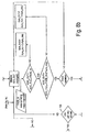
- FIG 2 is a block diagram of a radio receiver 20 with an analog-to-digital converter 22 (ADC) having dynamic range control according to the present invention. It shows a radio frequency receiver with a CDMA processing block (RAKE) 38 which is shown separately from other channel decoding functions. CDMA signal processing techniques other than RAKE can also be used in the digital architecture.
- Radio receiver 20 has one downconverting stage and can have several intermediate frequencies. It digitizes the signal received at antenna 24 from baseband, from any intermediate frequency, or directly from the incoming radio frequency of the associated radio frequency channel.
- the receiver can have in-phase and quadrature branches similar to the in-phase and quadrature branches shown in Figure 1 , which is block diagram of a conventional direct conversion receiver with associated gain control.
- ADC_ALERT alert value when RSSI is close to the ADC output value ADC_FULL full scale value or resolution of an ADC ADC_IN signal level at the input of an ADC ADC_N number of bits or resolution of an ADC ADC_OUT signal level at the output of an ADC ADC_OUT_TH threshold value of acceptable changes in ADC output value ALERT_N increase in ADC resolution when alert procedure is performed Apre_Av gain in the amplifier before an ADC (present also the total BB gain if needed) Aprev_Av_max maximum gain in the amplifier before an ADC Apre_step gain step of the amplifier before an ADC ASIC application specific integrated circuit BB baseband BER bit error rate BLER block error rate CDMA code division multiple access CPU central processing unit DECODE_DPCH dynamic range (or resolution) needed for decoding
- DPCH dedicated physical channel means unspreaded information DPCH dedicated physical channel.
- Term refers to WCDMA system terminology but here it can be considered generally as a single code channel in any CDMA system
- DSP digital signal processing FADE_M fading margin IF intermediate frequency LNA low noise amplifier
- QoS can have different meanings at different abstraction levels.
- QoS stands for the received signal quality with respect to data rate, spreading factor (only CDMA), SNR requirement and BER or BLER requirement.
- the method of the present invention is able to scale the high resolution ADC to the minimum number of bits (minimum dynamic range) required for decoding of the signal received from antenna 24 in view of the current radio receiving conditions.
- Most of the blocks shown in Figure 2 are conventional to a direct conversion receiver, including the power detector blocks 42, 48, 50 and 52, and with the exception of the control logic block 44 and the block 46 associated with target values from the digital signal processor, in addition to the high resolution ADC 22. All of the blocks are identified in Table 2.
- the block diagram of the radio receiver shown in Figure 2 does not require automatic gain control if the ADC 22 has sufficiently high resolution for receiving the desired radio channel under adverse receiving conditions. Thus a high resolution is needed for weak radio channels even in the case where no large interfering channels are present.
- the present invention can accommodate automatic gain control so as to control the gain of associated analog variable amplifiers 28 and 34 via control lines 54 and 56.
- the analog gain control scheme can be used to amplify weak signals more when relatively little power exists at other nearby radio channels so as to be able to scale down the resolution of the ADC and thus further reduce power consumption.
- Solid lines 58, 60, 62 and 64 in Figure 2 represent the repetitive control of the dynamic range of the ADC without associated automatic gain control.
- the target value from the digital signal processor represents the number of bits (or the dynamic resolution) required for decoding the radio channel at channel decoder 40 when other radio channels are filtered out (no interference) and the signal level at the input of a detector is correct.
- This target value is called TARGET_N. This number can be fixed and based upon the type of decoding to be performed or this number can be determined according to the specific mode in which the receiver is operating at some time or it can change during reception if the required value can be reevaluated according to existing conditions and service quality requirements.
- the required resolution for ADC 22 would be four to six bits.
- the received signal strength (RSSI) of the received radio channel is then measured and the required resolution calculated in a manner shown in Figure 3 with typical signal levels and required dynamic range vs. full-scale (full-resolution) of the ADC.
- Figures 4a, 4b, 4c illustrate various situations regarding ADC resolution calculation and will be described more fully below.
- the received signal strength RSSI is continuously measured by power detector 42 and if the value goes above or below a certain threshold value, the required resolution (number of bits) for the ADC is recalculated by control logic 44 and presented to the ADC via control line 64. In most situations it is necessary to average all of the measured signals so as to prevent reaction of the control to the normal ripple found in modulated signals or sources of distortion or noise. This is shown and explained in Figure 3 for the situation in which automatic gain control is not used.
- the method for continuously controlling the dynamic range of the ADC is shown in a situation where analog gain control is not used.
- the ADC is set to full-resolution and the target resolution for demodulation is received from the digital signal processor.
- quality of service QoS
- QoS quality of service
- the target resolution for the ADC (TARGET_N) is thus presented to the resolution target request step 70 and at the same time the received signal strength (RSSI) is measured (and typically averaged) at step 72.
- the results of steps 70 and 72 are presented to the actual resolution determination step 74.
- ADC_N ADC_FULL - RSSI + TARGET_N, where ADC_N represents a number of bits (or dynamic resolution) of the ADC under current operating conditions.
- ADC_N m + TARGET_N
- ADC_N (ADC_FULL - RSSI - 1.76 dB)/6.02 + TARGET_N.
- ADC_FULL and RSSI are given in decibels and ADC_N and TARGET_N in bits.
- Figure 4a shows that when the received signal strength is low, the number of bits (ADC_N) to be used by ADC 22 is relatively large and is only somewhat less than the maximum resolution of the ADC as set forth by variable ADC_FULL.
- Figure 4b shows the same situation in which the received signal strength is large, representing a good incoming signal and therefore the value of ADC_N is only slightly greater than the value of TARGET_N.
- module 76 sets the variable RSSI_TARGET to be equal to the current received signal strength RSSI. Then RSSI is again measured and averaged at step 78. Decisional block 80 determines if RSSI_TARGET minus the RSSI threshold (RSSI_TH) is less than the current measurement of RSSI as determined by step 78 and further if the current value of RSSI is less than the target value plus the RSSI threshold. If the result of the decisional block is true, the RSSI value is again measured and averaged (return to step 78), otherwise the resolution is again determined (return to step 74).
- RSSI_TARGET minus the RSSI threshold
- Measured RSSI and the predetermined target resolution (TARGET_N) are the main parameters calculated as shown in step 74, in order to determine the required resolution of the ADC.
- other parameters are used to determine the dynamic range and therefore bit resolution for the ADC, including estimating signal-to-interference ratio (SIR) and received power of the desired CDMA channel (DPCH_Ec) so as to improve the accuracy of the calculation.
- SIR signal-to-interference ratio
- DPCH_Ec received power of the desired CDMA channel
- parameters such as the power of the desired CDMA channel (DPCH_Ec) can be used to assist in the estimation of the required number of bits (TARGET_N) needed in CDMA systems for presentation to control logic. (optional line 61).
- ADC_N ADC_FULL - DPCH_Ec + DECODE_DPCH ; where DECODE_DPCH describes the required number of bits needed to decode the received information after despreading.
- TARGET_N can be defined in bits from the dynamic range as described earlier.
- This logic can be operated independently on the other algorithms and hence it can react faster to rapid changes. In most cases some averaging will be needed when DPCH_Ec or SIR_est is defined.
- Figure 5 shows a conventional analog gain control scheme which is used in many digital radio communication systems in order to optimize the level of the incoming radio frequency signal at the input of the analog-to-digital converter so as to be at a level which is best for ultimate detection.
- the methodology of Figure 5 can be applied in an embodiment of the invention for continuously controlling the dynamic range of the ADC by means of the flow chart set forth in Figure 6 .
- the signal level at the output of the ADC (ADC_OUT) is measured at step 82 such as by power detector 50 shown in Figure 2 .
- the gain in the (Aprev_Av) analog amplifier or amplifiers before the ADC is determined at step 84. This gain is then presented to the amplifier 34 as shown in Figure 2 via line 56.
- a similar amplification value can be determined for a low noise (RF) amplifier 28 by control logic 44 as presented to the LNA via control line 54. This is described more fully below with respect to Figure 8 .
- RF low noise
- Figure 6 shows that the remaining steps for performing the determination of ADC_N are similar to those in Figure 3 .
- Figure 6 represents an analog baseband gain control which is added to the resolution scaling method presented in Figure 3 .
- the overall result is seen as a reduction in the bit resolution for the ADC as seen in Figure 4d .
- the lines 71 between Figure 4c and Figure 4d qualitatively show this reduction in ADC_N for the same reception conditions.
- Figure 7 is a flow chart to define the ADC resolution with analog gain control which is more detailed than the flow chart shown in Figure 6 . Details are presented in Figure 7 for use of the fading margin (FADE_M) and the gain steps associated with amplifier 34 (Apre_step) so as to determine a new value of the amplifier gain (Apre_Av) as shown by steps 88 and 90, depending upon conditional modules 92 and 94 respectively.
- the lower portion of Figure 7 with respect to determining the current resolution to be used by the ADC (ADC_N) is basically similar to that shown in Figure 3 .
- the input level of the ADC is adjusted by adjusting the amplifier gain (Apre_Av) to an optimal level for presentation of the analog signal to the ADC.
- the fading margin (FADE_M) can be fixed or defined separately with respect to each mode of operation of the receiver. It also can be adjusted during radio channel reception.
- the resolution of the ADC is chosen based upon measured ADC_OUT and used in conjunction with the target resolution (TARGET_N) to determine an amount needed for signal detection at the channel decoder 40 (see Figure 2 ).
- the same method as shown in Figure 3 can be used. Using this method, the ADC resolution can be scaled down compared to implementations without high gain control.
- Figure 4d is an illustration when the received radio channel signal is weak and other channels are relatively weak with automatic gain control.
- a comparison of Figure 4c to Figure 4d shows that the reduction in ADC resolution as defined by ADC_N is a direct factor based upon the determined gain Apre_Av for use by amplifier 34.
- a radio frequency (RF) gain step is also used in many radio receivers.
- Figure 8 shows the flow chart associated with one embodiment of the present invention wherein the large gain step typical in RF circuitry is adopted for use by the ADC resolution control method according to the present invention. It should be noted that rather than the gain step being at the RF stage, it can also be performed at some intermediate frequency or at baseband stage and the same procedure can be applied in all these cases as well. The RF gain can be adjusted with smaller steps and all possible analog gain control schemes can be applied to the ADC resolution scaling method in a similar manner as presented here. It may be preferable to use RF gain control and eliminate analog baseband gain control as well, depending upon the particular application of the radio receiver. The same principle without baseband gain control as in Figure 8 can then be used.
- the control logic particular to the RF gain control is shown in steps 96, 98, 100, 102, 104, 106, 108, 110, 112, 114 and 116.
- the signal LNA_Av(n) is generated by control logic 44 shown in Figure 2 and presented via line 54 to the RF or low noise amplifier 28.
- the remaining flow steps shown in Figure 8 are similar to those shown in Figures 3 , 6 and 7 .
- the present invention can also generate an analog alert based upon measurements of received signal level fluctuations from an arbitrarily chosen test node.
- the overall principle of the analog alert is seen in Figure 9 .
- a specific example of an analog alert in combination with the continuous control of the dynamic range of ADC is presented in Figure 10 .
- either the resolution of the ADC as set by the method (ADC_N) or the gain of the amplifier 34 (Apre_Av), or both of these parameters can be modified based on the measurement of the test node. These values can be repetitively updated until an alert condition is not detected. Such a procedure reduces the latency associated with determination of ADC_N and gain when rapidly varying signal conditions are detected.
- the gain at the RF amplifier 28 can be modified if an analog alert is determined.
- the delay elements T1, T2, T3 and T4 seen in Figure 10 are used to unify the time difference between measured samples. Otherwise, each of the feedbacks may have different latencies which would cause non-unified measurement conditions.
- the alert process as shown in Figure 10 can be adapted to any of the previously defined algorithms such as seen in Figures 3 , 6 , 7 and 8 . The alert process thus reduces latency in the determination of ADC_N when rapidly changing signal conditions are detected.
- the implementation of the method for continuously controlling the dynamic range of the ADC can be performed with customized digital logic on the same chip in which the ADC is fabricated. This chip may be located on the same die with other RF parts or with the digital ASIC.
- the algorithms performed including those for calculating the dynamic range for the ADC, may be programmed into a digital signal processor and the measured data collected from other chips through busses connected to the DSP engine.
- a central processing unit can perform the calculations required by the method as well.
- customized digital logic would normally be the preferred method of implementation.
- a method for continuously determining the required dynamic range for an analog-to-digital converter thereby allows for a reduction in power consumption associated with the ADC, especially when the incoming signal is being received with few interfering radio channels and with a relatively high signal strength.
- the present method can be combined with analog gain control, as well as RF or IF gain control so as to further reduce the dynamic range necessary for decoding a received radio channel and thereby minimizing power consumption for these portions of a direct conversion radio receiver or any other receiver architecture.
- An alarm alert can be used to reduce the latency of ADC resolution calculation when rapidly fluctuating signal conditions are sensed. The method and apparatus for performing same are set forth and described herein above.
Claims (55)
- Steuermodul, welches umfasst:Steuerlogik (44), die konfiguriert ist, um detektierte, zu einem digitalen Ausgangssignal eines Analog-Digital-Wandlers (22) gehörige Werte zu empfangen, und konfiguriert ist, eine Arbeitsauflösung des Analog-Digital-Wandlers auf der Grundlage der detektierten Werte, eine Skalenendwertauflösung des Analog-Digital-Wandlers (22) und eine Zielauflösung zu bestimmen, die eine Auflösung angibt, die notwendig ist, um einen Funkkanal zu dekodieren, unter der Annahme, dass keine Interferenz von möglicherweise interferierenden Funkkanälen auftritt, wobei der Funkkanal ein Codemultiplexkanal ist, der eine Spreizspektrumsübertragung übermittelt;wobei die detektierten Werte einen ersten Signalparameter und einen zweiten Signalparameter umfassen;
dadurch gekennzeichnet, dass:der erste Signalparameter auf einem Signal basiert, das zum digitalen Ausgangssignal nach dem Filtern und Entspreizen gehört; undder zweite Signalparameter auf einem Signal basiert, das zu einem digitalen Ausgangssignal des Analog-Digital-Wandlers (22) vor dem Filtern gehört. - Steuermodul gemäß Anspruch 1, wobei die Steuerlogik (44) konfiguriert ist, um die detektierten Werte wiederholt zu empfangen und die Arbeitsauflösung wiederholt zu bestimmen.
- Steuermodul gemäß Anspruch 1 oder 2, wobei die Steuerlogik (44) konfiguriert ist, um ein Signal zum empfangen, das eine Ausgabe wenigstens eines Verstärkers (34), der zur Erzeugung der detektierten Werte gehört, angibt und um ein Signal zum Anpassen einer Verstärkung des wenigstens einen Verstärkers zu erzeugen.
- Steuermodul gemäß Anspruch 3, wobei die Steuerlogik (44) konfiguriert ist, um ein Signal zum Anpassen einer Verstärkung des wenigstens einen Verstärkers (34) zu erzeugen, um die Arbeitsauflösung des Analog-Digital-Wandlers (22) zu reduzieren.
- Steuermodul eines der vorhergehenden Ansprüche, wobei der erste Signalparameter ein Wert eines empfangenen Codekanals ist.
- Steuermodul eines der vorhergehenden Ansprüche, wobei die Zielauflösung eine Anzahl von Bits ist, die benötigt werden, um empfangene Information in einem empfangenen Codekanal nach einem Entspreizen der Übertragung des Funkkanals zu dekodieren.
- Steuermodul gemäß einem der Ansprüche 1 bis 4, wobei der erste Signalparameter ein Signal-zu-Interferenz Verhältnis des Funkkanals ist.
- Steuermodul gemäß Anspruch 5 oder 6, wobei der erste Signalparameter eine Leistung des Codemultiplexkanals ist.
- Vorrichtung, welche umfasst:ein Steuermodul (44) gemäß Anspruch 1 oder 2;den Analog-Digital-Wandler (22), der ausgelegt ist, um bei der Arbeitsauflösung ein zum Funkkanal gehöriges Signal in das digitale Ausgangssignal zu wandeln; undein erster und zweiter Detektor (52, 50), die ausgelegt sind, um den ersten bzw. zweiten Signalparameter zu messen.
- Vorrichtung gemäß Anspruch 9, wobei die Steuerlogik (44) konfiguriert ist, um wiederholt die Arbeitsauflösung zu bestimmen, falls der erste Signalparameter außerhalb vorbestimmter Grenzen für das Messen des ersten Signalparameters ist.
- Vorrichtung gemäß Anspruch 9, wobei die Steuerlogik (44) konfiguriert ist, um zu bestimmen, ob der zweite Signalparameter sich schneller ändert als ein vorbestimmter Betrag und, falls dem so ist, um die wiederholte Bestimmung der Betriebslösung zu modifizieren.
- Vorrichtung gemäß Anspruch 11, wobei der zweite Leistungsdetektor (50) mit dem Ausgang des Analog-Digital-Wandlers (22) verbunden ist.
- Vorrichtung gemäß Anspruch 10, 11 oder 12, wobei die Grenzen auf einem Schwellwert basieren.
- Vorrichtung gemäß Anspruch 13, wobei der Schwellwert ein vorbestimmter Schwellwert für den ersten Signalparameter ist.
- Vorrichtung gemäß Anspruch 9, wobei die Steuerlogik (44) konfiguriert ist, den ersten Signalparameter wiederholt zu aktualisieren, falls der erste Signalparameter innerhalb der Grenzen ist.
- Vorrichtung gemäß einem der Ansprüche 9 bis 15, welche ferner wenigstens einen Verstärker (28, 34) umfasst zum Verstärken des zum Funkkanal gehörigen Signals vor einem Bereitstellen des Signals einem Analog-Digital-Wandler (22).
- Vorrichtung gemäß Anspruch 16, wobei das Signal, das zu dem Funkkanal gehört, ein Signal in einem Funkfrequenzbereich ist, wobei der wenigstens eine Verstärker (28, 34) einen Funkfrequenzverstärker (28) zum Verstärken des Signals, während es in dem Funkfrequenzbereich ist, umfasst.
- Vorrichtung gemäß Anspruch 16 oder 17, wobei der wenigstens eine Verstärker (28, 34) eine anpassbare Verstärkung hat und wobei die Steuerlogik (44) konfiguriert ist, um die anpassbare Verstärkung wenigstens auf der Grundlage des digitalen Ausgangssignals des Analog-Digital-Wandlers (22) anzupassen.
- Vorrichtung gemäß Anspruch 18, wobei die Verstärkung des wenigstens einen Verstärkers (34) anpassbar ist auf der Grundlage wenigstens des Ausgangssignals des Analog-Digital-Wandlers (22), eines schwächer werdenden Rands und der Skalenendwertauflösung des Analog-Digital-Wandlers (22).
- Vorrichtung gemäß Anspruch 18, wobei die Steuerlogik (44) konfiguriert ist, um zu bestimmen, ob der zweite Signalparameter sich schneller ändert als ein vorbestimmter Betrag über eine Zeitdauer, und falls dem so ist, das Anpassen der Verstärkung des wenigstens einen Verstärkers (34) zu modifizieren.
- Vorrichtung gemäß Anspruch 18, wobei die Steuerlogik (44) konfiguriert ist, um die Verstärkung des wenigstens einen Verstärkers (34) durch Vergleich der digitalen Ausgabe mit einem Wert anzupassen, der wenigstens auf der Skalenendwertauflösung und einem weiteren Wert basiert.
- Vorrichtung gemäß Anspruch 21, wobei der weitere Wert wenigstens auf einem schwächer werdenden Rand basiert.
- Vorrichtung gemäß einem der Ansprüche 9 bis 22, wobei der erste Signalparameter auf einem Mittel von Messungen des ersten Signalparameters basiert.
- Vorrichtung gemäß einem der Ansprüche 9 bis 23, wobei der zweite Leistungsdetektor (50) konfiguriert ist, um den zweiten Signalparameter zu mitteln.
- Vorrichtung gemäß einem der Ansprüche 9 bis 24, wobei der zweite Codemultiplexkanal ein Breitband Codemultiplexkanal ist.
- Vorrichtung gemäß Anspruch 25, wobei der erste Leistungsdetektor (52) ausgelegt ist, um die Leistung eines empfangenen Codekanals zu messen.
- Vorrichtung gemäß einem der Ansprüche 9 bis 26, wobei die Zielauflösung eine Anzahl an Bits ist, die benötigt werden, um empfangene Information in einem empfangenen Codekanal nach Entspreizen der Übertragung des Funkkanals zu dekodieren.
- Vorrichtung gemäß einem der Ansprüche 9 bis 25, wobei der erste Leistungsdetektor (52) ausgelegt ist, ein Signal-zu-Interferenz-Verhältnis zu schätzen.
- Vorrichtung gemäß Anspruch 28, wobei die Steuerlogik (44) konfiguriert ist, um zu bestimmen, ob das geschätzte Signal-zu-Interferenz-Verhältnis kleiner als ein akzeptables Signal-Interferenz-Verhältnis ist und wobei die bestimmte Arbeitsauflösung eine Anzahl von Bits ist und um wenigstens ein Bit vergrößert wird, falls die Bestimmung gemacht wird.
- Vorrichtung gemäß Anspruch 29, wobei die Vergrößerung in der Arbeitsauflösung auf einer vorbestimmten Zahl basiert.
- Vorrichtung gemäß einem der Ansprüche 9 bis 16, welche ferner einen Funkfrequenzverstärker (28) umfasst zum Verstärken eines Signals, während es im Funkfrequenzbereich ist, sowie einen Mischer (30) zum Empfang der Ausgabe des Funkfrequenzverstärkers (28), um das zu einem Funkkanal gehörige Signal herzustellen.
- Vorrichtung gemäß Anspruch 31, wobei die Vorrichtung zum Messen der Ausgabe des Analog-Digital-Wandlers (22) konfiguriert ist und wobei die Steuerlogik (44) konfiguriert ist, um die Verstärkung des Funkfrequenzverstärkers (28) anzupassen, wenn die gemessene Ausgabe des Analog-Digital-Wandlers (22) größer als ein erster vorbestimmter Wert ist oder kleiner als ein zweiter Wert ist.
- Vorrichtung gemäß Anspruch 32, wobei der zweite Wert wenigstens auf einem zweiten vorbestimmten Wert basiert.
- Vorrichtung gemäß einem der Ansprüche 9 bis 25, wobei der erste Signalparameter ein Signal-zu-Interferenz-Verhältnis des Funkkanals ist.
- Vorrichtung gemäß Anspruch 9 bis 34, wobei die Zielauflösung wenigstens auf einer Codekanalleistung basiert.
- Vorrichtung gemäß einem der Ansprüche 9 bis 35, die zur Verwendung in einem zellulären Kommunikationssystem konfiguriert ist.
- Funkempfänger, welcher umfasst:eine Vorrichtung gemäß Anspruch 9; undeinen Decoder (40), der ausgelegt ist, um in Kommunikation mit dem digitalen Ausgangssignal zu sein, um den Funkkanal zu dekodieren.
- Funkempfänger gemäß Anspruch 37, wobei die Steuerlogik (44) konfiguriert ist, um zu bestimmen, ob der zweite Signalparameter sich schneller ändert als ein vorbestimmter Betrag, und falls dem so ist, konfiguriert ist, um die wiederholte Bestimmung der Arbeitsauflösung zu modifizieren.
- Funkempfänger gemäß Anspruch 37 oder 38, welcher ferner wenigstens einen Verstärker (28, 34) umfasst zum Verstärken des zu dem Funkkanal gehörigen Signals vor dem Bereitstellen des Signals dem Analog-Digital-Wandler (22).
- Funkempfänger gemäß Anspruch 39, wobei das zum Funkkanal gehörige Signal ein Signal in einem Funkfrequenzbereich ist, wobei der wenigstens eine Verstärker (28, 34) einen ersten Verstärker (34) zum Verstärken des Signals umfasst, nachdem das Signal durch einen Mischer (30) gegangen ist, sowie einen zweiten Verstärker, in der Form eines Funkfrequenzverstärker (28), zum Verstärken des Signals, während es im Funkfrequenzbereich ist, vor einem Bereitstellen des Signals dem Mischer (30).
- Verfahren, welches umfasst:Durchführen einer Analog-Digital-Wandlung bei einer Arbeitsauflösung eines zu einem Funkkanal gehörigen Signals in ein digitales Ausgangssignal, wobei der Funkkanal ein Codemultiplexkanal ist, der eine Spreizspektrumsübertragung übermittelt;Messen eines ersten Signalparameters des Funkkanals;Messen eines zweiten Signalparameters; undBestimmen der Arbeitsauflösung auf der Grundlage einer Skalenendwertauflösung, einer Zielauflösung und des ersten und zweiten Signalparameters, wobei die Zielauflösung eine Auflösung ist, die notwendig ist, um den Funkkanal zu dekodieren unter der Annahme, dass keine Interferenz aus möglicherweise interferierenden Funkkanälen auftritt;dadurch gekennzeichnet, dass:der erste Signalparameter auf einem Signal basiert, das zu dem digitalen Ausgangssignal nach dem Filtern und Entspreizen gehört; undder zweite Signalparameter auf einem Signal basiert, das zu dem digitalen Ausgangssignal vor dem Filtern gehört.
- Verfahren gemäß Anspruch 41, wobei das Bestimmen der Arbeitsauflösung wiederholt durchgeführt wird.
- Verfahren gemäß Anspruch 42, welches ferner ein Modifizieren der wiederholten Bestimmung der Arbeitsauflösung umfasst, wenn der zweite Signalparameter sich schneller als ein vorbestimmter Betrag ändert.
- Verfahren gemäß Anspruch 42, wobei das Bestimmen der Arbeitsauflösung wiederholt durchgeführt wird, falls der erste Signalparameter außerhalb von Grenzen ist, die für die Messungen des ersten Signalparameters spezifiziert sind.
- Verfahren gemäß Anspruch 44, wobei die Grenzen auf einem vorbestimmten Schwellwert des ersten Signalparameters basieren.
- Verfahren gemäß einem der Ansprüche 41 bis 45, welches ferner ein Verstärken des zu dem Funkkanal gehörigen Signals umfasst, vor einem Wandeln des Signals in ein digitales Ausgangssignal.
- Verfahren gemäß Anspruch 46, wobei das Verstärken ein Anpassen der Verstärkung des Verstärkers (28, 34) umfasst, um die Arbeitsauflösung zu reduzieren.
- Verfahren gemäß Anspruch 47, wobei die anpassbare Verstärkung durch Vergleichen des digitalen Ausgangssignals mit einem Wert angepasst wird, der wenigstens auf der Skalenendwertauflösung und einem weiteren Wert basiert.
- Verfahren gemäß Anspruch 48, wobei der weitere Wert wenigstens auf einem schwächer werdenden Rand basiert.
- Verfahren gemäß einem der Ansprüche 41 bis 45, wobei das zu dem Funkkanal gehörige Signal ein Signal in einem Funkfrequenzbereich ist, wobei das Verfahren ferner ein Verstärken des Signals umfasst, während es im Funkfrequenzbereich ist.
- Verfahren gemäß Anspruch 50, wobei das Verstärken ein Anpassen der Verstärkung eines Verstärkers (28, 34) umfasst, um die bestimmte Arbeitsauflösung zu reduzieren.
- Verfahren gemäß einem der Ansprüche 41 bis 51, wobei das Messen des ersten Signalparameters des Funkkanals auf einem Mittel von Messungen des ersten Signalparameters basiert.
- Verfahren gemäß einem der Ansprüche 41 bis 52, wobei der erste Signalparameter ein Signal-zu-Interferenz-Verhältnis des Funkkanals ist.
- Verfahren gemäß einem der Ansprüche 41 bis 52, wobei der erste Signalparameter eine empfangene Leistung eines Codemultiplexkanals umfasst.
- Verfahren gemäß einem der Ansprüche 41 bis 54, wobei die Zielauflösung wenigstens auf einer Codekanalleistung basiert.
Applications Claiming Priority (2)
| Application Number | Priority Date | Filing Date | Title |
|---|---|---|---|
| US09/977,271 US6993291B2 (en) | 2001-10-11 | 2001-10-11 | Method and apparatus for continuously controlling the dynamic range from an analog-to-digital converter |
| EP02256547A EP1303053B1 (de) | 2001-10-11 | 2002-09-20 | Verfahren und Einrichtung zur kontinuierlichen Steuerung des dynamischen Bereichs eines Analog-Digital-Wandlers |
Related Parent Applications (1)
| Application Number | Title | Priority Date | Filing Date |
|---|---|---|---|
| EP02256547A Division EP1303053B1 (de) | 2001-10-11 | 2002-09-20 | Verfahren und Einrichtung zur kontinuierlichen Steuerung des dynamischen Bereichs eines Analog-Digital-Wandlers |
Publications (2)
| Publication Number | Publication Date |
|---|---|
| EP1655848A1 EP1655848A1 (de) | 2006-05-10 |
| EP1655848B1 true EP1655848B1 (de) | 2008-11-26 |
Family
ID=25524979
Family Applications (2)
| Application Number | Title | Priority Date | Filing Date |
|---|---|---|---|
| EP02256547A Expired - Lifetime EP1303053B1 (de) | 2001-10-11 | 2002-09-20 | Verfahren und Einrichtung zur kontinuierlichen Steuerung des dynamischen Bereichs eines Analog-Digital-Wandlers |
| EP05112836A Expired - Lifetime EP1655848B1 (de) | 2001-10-11 | 2002-09-20 | Verfahren und Einrichtung zur kontinuierlichen Steuerung des dynamischen Bereichs eines Analog-Digital-Wandlers |
Family Applications Before (1)
| Application Number | Title | Priority Date | Filing Date |
|---|---|---|---|
| EP02256547A Expired - Lifetime EP1303053B1 (de) | 2001-10-11 | 2002-09-20 | Verfahren und Einrichtung zur kontinuierlichen Steuerung des dynamischen Bereichs eines Analog-Digital-Wandlers |
Country Status (3)
| Country | Link |
|---|---|
| US (2) | US6993291B2 (de) |
| EP (2) | EP1303053B1 (de) |
| DE (2) | DE60230076D1 (de) |
Cited By (2)
| Publication number | Priority date | Publication date | Assignee | Title |
|---|---|---|---|---|
| US9750947B2 (en) | 2009-10-27 | 2017-09-05 | St. Jude Medical Ab | Power saving communication method for an implantable medical device |
| US11550015B2 (en) | 2020-04-28 | 2023-01-10 | Lake Shore Cryotronics, Inc. | Ranging systems and methods for decreasing transitive effects in multi-range materials measurements |
Families Citing this family (146)
| Publication number | Priority date | Publication date | Assignee | Title |
|---|---|---|---|---|
| US7151759B1 (en) * | 2001-03-19 | 2006-12-19 | Cisco Systems Wireless Networking (Australia) Pty Limited | Automatic gain control and low power start-of-packet detection for a wireless LAN receiver |
| US6993291B2 (en) * | 2001-10-11 | 2006-01-31 | Nokia Corporation | Method and apparatus for continuously controlling the dynamic range from an analog-to-digital converter |
| US7212586B2 (en) * | 2002-01-18 | 2007-05-01 | Broadcom Corporation | Direct conversion RF transceiver for wireless communications |
| US7295645B1 (en) * | 2002-01-29 | 2007-11-13 | Ellipsis Digital Systems, Inc. | System, method and apparatus to implement low power high performance transceivers with scalable analog to digital conversion resolution and dynamic range |
| US20030162518A1 (en) * | 2002-02-22 | 2003-08-28 | Baldwin Keith R. | Rapid acquisition and tracking system for a wireless packet-based communication device |
| US7376174B2 (en) * | 2002-06-07 | 2008-05-20 | Texas Instruments Incorporated | Rake receiver architecture for an ultra-wideband (UWB) receiver |
| US7218905B1 (en) * | 2002-06-14 | 2007-05-15 | Skyworks Solutions, Inc. | Gain compensation |
| US7295812B2 (en) * | 2002-06-26 | 2007-11-13 | Nokia Corporation | Method and apparatus providing adaptable current consumption for mobile station based on macrocell/microcell determination |
| DE10241554A1 (de) * | 2002-09-05 | 2004-03-25 | Schleifring Und Apparatebau Gmbh | Empfangseinrichtung für digitale Signale |
| DE10241583B4 (de) * | 2002-09-05 | 2005-09-01 | Schleifring Und Apparatebau Gmbh | Empfangseinrichtung für digitale Signale |
| US7430406B2 (en) * | 2002-11-08 | 2008-09-30 | Qualcomm Incorporated | Gain control in a wireless device |
| KR20050074630A (ko) * | 2002-11-18 | 2005-07-18 | 코닌클리즈케 필립스 일렉트로닉스 엔.브이. | 무선 수신기 및 그 작동 방법, a/d 변환기의 포화 방지방법 |
| US6950641B2 (en) * | 2003-01-31 | 2005-09-27 | Nokia Corporation | Apparatus, and an associated method, for increasing receiver sensitivity of a direct conversion receiver |
| ATE379880T1 (de) * | 2003-02-11 | 2007-12-15 | Ericsson Telefon Ab L M | Interferenzermittlung in einem mobilkommunikationssystem |
| TWI355798B (en) * | 2003-03-12 | 2012-01-01 | St Ericsson Sa | Automatic gain control with two power detectors |
| PL359304A1 (en) * | 2003-03-24 | 2004-10-04 | Advanced Digital Broadcast Ltd. | Method for calibration of signal receiver equipped with automatic gain control circuits |
| CN1549454A (zh) * | 2003-05-16 | 2004-11-24 | 皇家飞利浦电子股份有限公司 | 具有一个有限动态范围的adc的无线通信接收机 |
| US7212798B1 (en) | 2003-07-17 | 2007-05-01 | Cisco Technology, Inc. | Adaptive AGC in a wireless network receiver |
| US8401128B2 (en) * | 2003-08-28 | 2013-03-19 | Telefonaktiebolaget L M Ericsson (Publ) | Method and system for adaptable receiver parameters |
| US7587175B2 (en) * | 2003-10-20 | 2009-09-08 | Broadcom Corporation | Radio frequency unit analog level detector and feedback control system |
| US6864817B1 (en) * | 2003-12-30 | 2005-03-08 | Freescale Semiconductor, Inc. | Signaling dependent adaptive analog-to-digital converter (ADC) system and method of using same |
| US7203476B2 (en) * | 2004-01-09 | 2007-04-10 | Motorola, Inc. | Method and apparatus for minimizing baseband offset error in a receiver |
| CA2560737A1 (en) | 2004-04-09 | 2005-10-27 | Micronas Semiconductors, Inc. | Apparatus for and method of controlling the operation of an equalizer |
| EP1605587A1 (de) * | 2004-06-07 | 2005-12-14 | Infineon Technologies AG | Ein Empfänger beinhaltet in einem Funkkommunicationssystem |
| US7372925B2 (en) * | 2004-06-09 | 2008-05-13 | Theta Microelectronics, Inc. | Wireless LAN receiver with I and Q RF and baseband AGC loops and DC offset cancellation |
| JP3887000B2 (ja) * | 2004-06-11 | 2007-02-28 | シャープ株式会社 | 電子回路装置 |
| US7274920B2 (en) * | 2004-06-30 | 2007-09-25 | Research In Motion Limited | Methods and apparatus for reducing signal interference in a wireless receiver based on signal-to-interference ratio |
| WO2006020950A1 (en) * | 2004-08-12 | 2006-02-23 | Micronas Semiconductors, Inc. | Automatic gain control unit of a receiver |
| WO2006040390A1 (en) * | 2004-10-15 | 2006-04-20 | Nokia Corporation | Reduction of power consumption in wireless communication terminals |
| KR100598696B1 (ko) * | 2004-12-17 | 2006-07-10 | 인티그런트 테크놀로지즈(주) | 전력 검출 회로를 포함하는 자동 이득 제어 회로. |
| US7769108B1 (en) * | 2004-12-17 | 2010-08-03 | The United States Of America As Represented By The Secretary Of The Air Force | Digital receiver instantaneous dynamic range enhancement |
| ATE538557T1 (de) * | 2005-03-04 | 2012-01-15 | Nokia Corp | Streckenherstellung in einer drahtlosen kommunikationsumgebung |
| GB2439685B (en) * | 2005-03-24 | 2010-04-28 | Siport Inc | Low power digital media broadcast receiver with time division |
| US7916711B2 (en) * | 2005-03-24 | 2011-03-29 | Siport, Inc. | Systems and methods for saving power in a digital broadcast receiver |
| US20060222115A1 (en) * | 2005-03-30 | 2006-10-05 | Silicon Laboratories, Inc. | Television receiver with automatic gain control (AGC) |
| US20060229025A1 (en) * | 2005-03-30 | 2006-10-12 | Lucent Technologies Inc. | Method for extracting optimal reverse link capacity by scaling reverse link Eb/No setpoint based on aggregate channel load and condition |
| US7262724B2 (en) * | 2005-03-31 | 2007-08-28 | Freescale Semiconductor, Inc. | System and method for adjusting dynamic range of analog-to-digital converter |
| CN101176260A (zh) * | 2005-04-01 | 2008-05-07 | Nxp股份有限公司 | 信号强度指示器 |
| US7945233B2 (en) * | 2005-06-16 | 2011-05-17 | Siport, Inc. | Systems and methods for dynamically controlling a tuner |
| US7426376B2 (en) * | 2005-06-30 | 2008-09-16 | Silicon Laboratories Inc. | Receiver having digital automatic gain control |
| US8335484B1 (en) * | 2005-07-29 | 2012-12-18 | Siport, Inc. | Systems and methods for dynamically controlling an analog-to-digital converter |
| WO2007022417A2 (en) * | 2005-08-18 | 2007-02-22 | Wionics Research | Automatic gain control for frequency-hopped ofdm |
| US7593484B2 (en) * | 2005-09-30 | 2009-09-22 | Skyworks Solutions, Inc. | Radio frequency (RF) receiver with double loop integrated fast response automatic gain control (AGC) |
| US7515888B2 (en) * | 2005-10-06 | 2009-04-07 | Nxp B.V. | Systems and method for a highly integrated, multi-mode tuner |
| US7664211B2 (en) | 2005-10-07 | 2010-02-16 | Starkey Laboratories, Inc. | Automatic gain control with out of band blocking signal compensation |
| US7242334B2 (en) * | 2005-12-09 | 2007-07-10 | Sirific Wireless Corporation | Wireless receiver circuit with merged ADC and filter |
| US9401843B2 (en) * | 2006-01-27 | 2016-07-26 | Telefonaktiebolaget Lm Ericsson (Publ) | Method and apparatus for reverse link control in a wireless communication network as a function of reverse link load characteristic |
| US20070223626A1 (en) * | 2006-03-21 | 2007-09-27 | Shay Waxman | Dynamic analog power management in mobile station receivers |
| US7570934B2 (en) | 2006-04-18 | 2009-08-04 | Analog Devices, Inc. | Automatic gain control circuit |
| US8045927B2 (en) * | 2006-04-27 | 2011-10-25 | Nokia Corporation | Signal detection in multicarrier communication system |
| US7853227B2 (en) * | 2006-05-26 | 2010-12-14 | Microtune (Texas), L.P. | AGC system and method for broadband tuners |
| US20110025396A1 (en) * | 2006-05-26 | 2011-02-03 | Microtune (Texas), L.P. | Digital Attenuator Circuits and Methods for Use thereof |
| US7477085B2 (en) * | 2006-05-26 | 2009-01-13 | Microtune (Texas), L.P. | Digital attenuator circuits and methods for use thereof |
| US7653368B2 (en) * | 2006-06-14 | 2010-01-26 | Intel Corporation | Radio receiver and a method thereof |
| JP2008042765A (ja) * | 2006-08-09 | 2008-02-21 | Sharp Corp | 受信システム |
| US7965208B2 (en) * | 2006-08-11 | 2011-06-21 | Entegris, Inc. | Auto ranging system and method for analog signal |
| GB2440988A (en) * | 2006-08-18 | 2008-02-20 | Iti Scotland Ltd | Wireless receiver with low resolution ADC power saving mode |
| US7656970B1 (en) * | 2006-09-01 | 2010-02-02 | Redpine Signals, Inc. | Apparatus for a wireless communications system using signal energy to control sample resolution and rate |
| KR100788637B1 (ko) * | 2006-10-02 | 2007-12-26 | (주)에프씨아이 | 이득제어 및 다중대역의 처리가 가능한 수신기 |
| US7688237B2 (en) * | 2006-12-21 | 2010-03-30 | Broadcom Corporation | Apparatus and method for analog-to-digital converter calibration |
| US7639998B1 (en) * | 2007-02-07 | 2009-12-29 | Rockwell Collins, Inc. | RF receiver utilizing dynamic power management |
| GB0703883D0 (en) * | 2007-02-28 | 2007-04-11 | Cambridge Silicon Radio Ltd | Receiver gain control |
| GB0704328D0 (en) * | 2007-03-06 | 2007-04-11 | Nokia Corp | Analogue-to-digital converter (adc) dynamic range and gain control |
| US8126101B2 (en) | 2007-03-27 | 2012-02-28 | Freescale Semiconductor, Inc. | Method and apparatus for varying a dynamic range |
| US7908082B2 (en) * | 2007-05-04 | 2011-03-15 | The Boeing Company | Methods and systems for displaying airport moving map information |
| US8199769B2 (en) | 2007-05-25 | 2012-06-12 | Siport, Inc. | Timeslot scheduling in digital audio and hybrid audio radio systems |
| US20090042527A1 (en) * | 2007-06-12 | 2009-02-12 | Hmicro Inc. | Dynamic low power receiver |
| US20090040107A1 (en) * | 2007-06-12 | 2009-02-12 | Hmicro, Inc. | Smart antenna subsystem |
| US8442476B2 (en) * | 2007-07-20 | 2013-05-14 | Cresta Technology Corporation | Mobile radio receiver power management systems and methods |
| US8577319B2 (en) * | 2007-10-10 | 2013-11-05 | Maxlinear, Inc. | Gain partitioning in a receiver |
| WO2009055714A2 (en) * | 2007-10-24 | 2009-04-30 | Hmicro, Inc. | Systems and networks for half and full duplex wireless communication using multiple radios |
| KR100916485B1 (ko) * | 2007-11-20 | 2009-09-08 | 삼성전기주식회사 | 시그마-델타 구조를 갖는 수신 장치 |
| US7965215B2 (en) * | 2007-12-12 | 2011-06-21 | Broadcom Corporation | Method and system for variable resolution data conversion in a receiver |
| US8447260B2 (en) * | 2007-12-12 | 2013-05-21 | Broadcom Corporation | Method and system for on-demand receiver supply voltage and current |
| US20090154612A1 (en) * | 2007-12-12 | 2009-06-18 | Ahmadreza Rofougaran | Method and system for dynamic filtering and data conversion resolution adjustments in a receiver |
| US8213872B2 (en) * | 2007-12-19 | 2012-07-03 | Rambus Inc. | Technique for low-power operation of a wireless device |
| WO2009100401A2 (en) | 2008-02-06 | 2009-08-13 | Hmicro, Inc. | Wireless communications systems using multiple radios |
| KR100966766B1 (ko) * | 2008-02-14 | 2010-07-01 | (주)에프씨아이 | 자동이득제어 정보를 이용한 전력소모 감소장치가 구비된수신기 및 이를 이용한 전력소모 감소방법 |
| KR100966767B1 (ko) * | 2008-02-14 | 2010-06-29 | (주)에프씨아이 | Gbw 최적화를 이용하여 전력소모를 감소시키는전류조절부가 구비된 수신기 |
| WO2009107359A1 (ja) * | 2008-02-29 | 2009-09-03 | パナソニック株式会社 | 増幅回路及びそれを用いた受信装置 |
| US7760122B1 (en) * | 2008-05-02 | 2010-07-20 | Pmc-Sierra, Inc. | Power optimized ADC for wireless transceivers |
| US8180308B1 (en) * | 2008-06-10 | 2012-05-15 | Marvell International Ltd. | Apparatus and methods for detection of interface in radio-frequency devices |
| US9219458B2 (en) * | 2008-06-12 | 2015-12-22 | Qualcomm Incorporated | Methods and systems of AGC and DC calibration for OFDM/OFDMA systems |
| US20100007355A1 (en) * | 2008-07-10 | 2010-01-14 | Litepoint Corporation | Method for testing radio frequency (rf) receiver to provide power correction data |
| US8467727B2 (en) | 2008-09-15 | 2013-06-18 | Sony Corporation | Controlling the dynamic range of a RF receiver circuit in a wireless communication terminal to reestablish a lost communication link |
| KR101544429B1 (ko) * | 2008-10-17 | 2015-08-17 | 삼성전자주식회사 | 이동통신 시스템의 이득 제어 장치 및 방법 |
| US7876251B2 (en) * | 2008-10-22 | 2011-01-25 | Siemens Medical Solutions Usa, Inc. | System for processing patient monitoring signals |
| US8731500B2 (en) * | 2009-01-29 | 2014-05-20 | Telefonaktiebolaget Lm Ericsson (Publ) | Automatic gain control based on bandwidth and delay spread |
| US8320823B2 (en) * | 2009-05-04 | 2012-11-27 | Siport, Inc. | Digital radio broadcast transmission using a table of contents |
| US8300680B2 (en) * | 2009-06-11 | 2012-10-30 | Qualcomm Incorporated | Apparatus and method for dynamic scaling of ADC sampling rate to avoid receiver interference |
| WO2011006585A2 (en) | 2009-07-16 | 2011-01-20 | Sony Corporation | Communications system using adaptive frequency notching |
| US9647623B2 (en) * | 2009-09-30 | 2017-05-09 | Silicon Laboratories Inc. | Signal processor suitable for low intermediate frequency (LIF) or zero intermediate frequency (ZIF) operation |
| WO2011053196A1 (en) * | 2009-10-27 | 2011-05-05 | St. Jude Medical Ab | Implantable medical device power saving communication |
| US8477887B2 (en) * | 2009-12-21 | 2013-07-02 | Qualcomm Incorporated | Systems and methods providing frequency-domain automatic gain control (AGC) |
| US8843094B2 (en) * | 2010-07-01 | 2014-09-23 | Broadcom Corporation | Method and system for blocker detecton and automatic gain control |
| US8587463B2 (en) * | 2010-08-16 | 2013-11-19 | The Regents Of The University Of California | Signal statistics and compression-based analog-to-digital converters |
| US8983416B1 (en) * | 2010-11-15 | 2015-03-17 | Csr Technology Inc. | Arbiter-based automatic gain control |
| US8489053B2 (en) | 2011-01-16 | 2013-07-16 | Siport, Inc. | Compensation of local oscillator phase jitter |
| US8989687B2 (en) | 2011-01-28 | 2015-03-24 | Broadcom Corporation | Communication receiver enhancements using multi-signal capture |
| JP5615203B2 (ja) * | 2011-02-24 | 2014-10-29 | パナソニック株式会社 | 自動利得制御装置 |
| US9172344B2 (en) | 2011-03-24 | 2015-10-27 | Silicon Laboratories Inc. | Statistical gain control in a receiver |
| US8891713B2 (en) | 2011-04-06 | 2014-11-18 | Siemens Medical Solutions Usa, Inc. | System for adaptive sampled medical signal interpolative reconstruction for use in patient monitoring |
| US8983418B2 (en) * | 2011-06-20 | 2015-03-17 | Broadcom Corporation | Multi-stage gain control in receivers and other circuits |
| US9059766B2 (en) * | 2011-07-15 | 2015-06-16 | Intel IP Corporation | System and method for controlling current to certain components of a wireless communication device |
| US20130044842A1 (en) * | 2011-08-19 | 2013-02-21 | Hong Kong Applied Science and Technology Research Institute Company Limited | Radio-frequency front ends with automatic gain control |
| CN106253905A (zh) * | 2011-08-19 | 2016-12-21 | 路梅戴尼科技公司 | 时域切换模拟数字转换器设备与方法 |
| EP2745409A4 (de) * | 2011-08-19 | 2015-07-15 | Lumedyne Technologies Inc | Zeitbereichsgeschaltete analog-digital-wandlervorrichtungen und -verfahren |
| TWI571064B (zh) * | 2011-08-19 | 2017-02-11 | 路梅戴尼科技公司 | 時域切換之類比至數位轉換器設備與方法 |
| US20130058439A1 (en) * | 2011-09-06 | 2013-03-07 | Ying-Yao Lin | Receiver |
| US8779961B2 (en) * | 2011-11-01 | 2014-07-15 | Marvell World Trade Ltd. | Scalable successive-approximation-register analog-to-digital converter |
| EP2608404B1 (de) | 2011-12-20 | 2016-07-27 | Telefonaktiebolaget LM Ericsson (publ) | Verfahren und Vorrichtung zur Durchführung einer automatischen Verstärkungsregelung eines empfangenen Signals |
| US9001941B2 (en) * | 2012-01-31 | 2015-04-07 | Analog Devices, Inc. | Method and apparatus to independently control front end gain and baseband gain |
| US8744390B2 (en) * | 2012-03-29 | 2014-06-03 | Adc Telecommunications, Inc. | Systems and methods for adjusting system tests based on detected interference |
| US9275690B2 (en) | 2012-05-30 | 2016-03-01 | Tahoe Rf Semiconductor, Inc. | Power management in an electronic system through reducing energy usage of a battery and/or controlling an output power of an amplifier thereof |
| US9509351B2 (en) | 2012-07-27 | 2016-11-29 | Tahoe Rf Semiconductor, Inc. | Simultaneous accommodation of a low power signal and an interfering signal in a radio frequency (RF) receiver |
| CN102821453B (zh) * | 2012-08-28 | 2018-11-20 | 中兴通讯股份有限公司 | 消除msr接收机gsm与lte干扰的自动增益调控方法及装置 |
| WO2014086021A1 (zh) * | 2012-12-06 | 2014-06-12 | 华为技术有限公司 | 一种接收信号强度指示的检测装置和方法 |
| US9184498B2 (en) | 2013-03-15 | 2015-11-10 | Gigoptix, Inc. | Extending beamforming capability of a coupled voltage controlled oscillator (VCO) array during local oscillator (LO) signal generation through fine control of a tunable frequency of a tank circuit of a VCO thereof |
| US9837714B2 (en) | 2013-03-15 | 2017-12-05 | Integrated Device Technology, Inc. | Extending beamforming capability of a coupled voltage controlled oscillator (VCO) array during local oscillator (LO) signal generation through a circular configuration thereof |
| US9780449B2 (en) | 2013-03-15 | 2017-10-03 | Integrated Device Technology, Inc. | Phase shift based improved reference input frequency signal injection into a coupled voltage controlled oscillator (VCO) array during local oscillator (LO) signal generation to reduce a phase-steering requirement during beamforming |
| US9531070B2 (en) | 2013-03-15 | 2016-12-27 | Christopher T. Schiller | Extending beamforming capability of a coupled voltage controlled oscillator (VCO) array during local oscillator (LO) signal generation through accommodating differential coupling between VCOs thereof |
| US9722310B2 (en) | 2013-03-15 | 2017-08-01 | Gigpeak, Inc. | Extending beamforming capability of a coupled voltage controlled oscillator (VCO) array during local oscillator (LO) signal generation through frequency multiplication |
| US9716315B2 (en) | 2013-03-15 | 2017-07-25 | Gigpeak, Inc. | Automatic high-resolution adaptive beam-steering |
| US9666942B2 (en) | 2013-03-15 | 2017-05-30 | Gigpeak, Inc. | Adaptive transmit array for beam-steering |
| EP3161416A2 (de) | 2014-06-26 | 2017-05-03 | Lumedyne Technologies Incorporated | Systeme und verfahren zur extraktion von systemparametern aus nichtlinearen periodischen signalen von sensoren |
| CN107636473B (zh) | 2015-05-20 | 2020-09-01 | 卢米达因科技公司 | 从非线性的周期性信号中提取惯性信息 |
| US10402251B2 (en) | 2015-07-24 | 2019-09-03 | Nxp Usa, Inc. | DMA controller for a data processing system, a data processing system and a method of operating a DMA controller |
| US10666370B2 (en) * | 2016-06-10 | 2020-05-26 | Apple Inc. | Multiple modulated spur cancellation apparatus |
| US10234477B2 (en) | 2016-07-27 | 2019-03-19 | Google Llc | Composite vibratory in-plane accelerometer |
| US10230384B2 (en) | 2016-12-09 | 2019-03-12 | Rambus Inc. | Variable resolution digital equalization |
| KR101877672B1 (ko) * | 2017-04-03 | 2018-07-11 | 엘에스산전 주식회사 | Ad컨버터 |
| US10014026B1 (en) | 2017-06-20 | 2018-07-03 | Seagate Technology Llc | Head delay calibration and tracking in MSMR systems |
| EP3477858B1 (de) | 2017-10-26 | 2022-10-05 | Nxp B.V. | Steuergerät für automatische verstärkung |
| US10297281B1 (en) | 2017-11-06 | 2019-05-21 | Seagate Technology Llc | Servo sector detection |
| CN109981066A (zh) * | 2017-12-27 | 2019-07-05 | 晨星半导体股份有限公司 | 自动增益控制装置与自动增益控制方法 |
| US11016681B1 (en) | 2018-07-31 | 2021-05-25 | Seagate Technology Llc | Multi-threshold parameter adaptation |
| US10522177B1 (en) | 2018-07-31 | 2019-12-31 | Seagate Technology Llc | Disc locked clock-based servo timing |
| US11018842B1 (en) | 2018-07-31 | 2021-05-25 | Seagate Technology Llc | Dynamic timing recovery bandwidth modulation for phase offset mitigation |
| US10727798B2 (en) | 2018-08-17 | 2020-07-28 | Invensense, Inc. | Method for improving die area and power efficiency in high dynamic range digital microphones |
| US10803902B1 (en) | 2018-08-19 | 2020-10-13 | Seagate Technology Llc | Hardware-based read sample averaging |
| US10460762B1 (en) | 2018-09-04 | 2019-10-29 | Seagate Technology Llc | Cancelling adjacent track interference signal with different data rate |
| US10468060B1 (en) | 2018-09-27 | 2019-11-05 | Seagate Technology Llc | Cancelling adjacent track interference |
| US10855308B2 (en) | 2018-11-19 | 2020-12-01 | Invensense, Inc. | Adaptive analog to digital converter (ADC) multipath digital microphones |
| US11139791B2 (en) * | 2019-09-18 | 2021-10-05 | Texas Instruments Incorporated | Integrated circuit devices with receiver chain peak detectors |
| JP7341964B2 (ja) * | 2020-09-15 | 2023-09-11 | 株式会社東芝 | 半導体装置 |
| US11888455B2 (en) | 2021-09-13 | 2024-01-30 | Invensense, Inc. | Machine learning glitch prediction |
Citations (1)
| Publication number | Priority date | Publication date | Assignee | Title |
|---|---|---|---|---|
| WO2001018970A1 (en) * | 1999-09-07 | 2001-03-15 | Telefonaktiebolaget Lm Ericsson (Publ) | Method and apparatus for adaptive bit resolution in a digital receiver and a digital transmitter |
Family Cites Families (8)
| Publication number | Priority date | Publication date | Assignee | Title |
|---|---|---|---|---|
| US4910752A (en) | 1987-06-15 | 1990-03-20 | Motorola, Inc. | Low power digital receiver |
| US5721756A (en) * | 1996-03-26 | 1998-02-24 | Sicom, Inc. | Digital receiver with tunable analog parameters and method therefor |
| US5926218A (en) * | 1996-06-04 | 1999-07-20 | Eastman Kodak Company | Electronic camera with dual resolution sensors |
| JP3186718B2 (ja) * | 1998-11-18 | 2001-07-11 | 日本電気株式会社 | キャリア検出回路 |
| GB9905997D0 (en) * | 1999-03-16 | 1999-05-12 | Koninkl Philips Electronics Nv | Radio receiver |
| US6686957B1 (en) * | 1999-03-31 | 2004-02-03 | Cirrus Logic, Inc. | Preview mode low resolution output system and method |
| US6843597B1 (en) * | 2001-05-15 | 2005-01-18 | Golden Bridge Technology Inc. | Method and apparatus of a fast two-loop automatic gain control circuit |
| US6993291B2 (en) * | 2001-10-11 | 2006-01-31 | Nokia Corporation | Method and apparatus for continuously controlling the dynamic range from an analog-to-digital converter |
-
2001
- 2001-10-11 US US09/977,271 patent/US6993291B2/en active Active
-
2002
- 2002-09-20 EP EP02256547A patent/EP1303053B1/de not_active Expired - Lifetime
- 2002-09-20 DE DE60230076T patent/DE60230076D1/de not_active Expired - Lifetime
- 2002-09-20 EP EP05112836A patent/EP1655848B1/de not_active Expired - Lifetime
- 2002-09-20 DE DE60209088T patent/DE60209088T2/de not_active Expired - Lifetime
-
2005
- 2005-11-21 US US11/285,541 patent/US7522885B2/en not_active Expired - Lifetime
Patent Citations (1)
| Publication number | Priority date | Publication date | Assignee | Title |
|---|---|---|---|---|
| WO2001018970A1 (en) * | 1999-09-07 | 2001-03-15 | Telefonaktiebolaget Lm Ericsson (Publ) | Method and apparatus for adaptive bit resolution in a digital receiver and a digital transmitter |
Cited By (4)
| Publication number | Priority date | Publication date | Assignee | Title |
|---|---|---|---|---|
| US9750947B2 (en) | 2009-10-27 | 2017-09-05 | St. Jude Medical Ab | Power saving communication method for an implantable medical device |
| US11550015B2 (en) | 2020-04-28 | 2023-01-10 | Lake Shore Cryotronics, Inc. | Ranging systems and methods for decreasing transitive effects in multi-range materials measurements |
| US11762050B2 (en) | 2020-04-28 | 2023-09-19 | Lake Shore Cryotronics, Inc. | Integrated measurement systems and methods for synchronous, accurate materials property measurement |
| US11959991B2 (en) | 2020-04-28 | 2024-04-16 | Lake Shore Cryotronics, Inc. | Hybrid digital and analog signal generation systems and methods |
Also Published As
| Publication number | Publication date |
|---|---|
| EP1303053B1 (de) | 2006-02-08 |
| DE60209088T2 (de) | 2006-08-03 |
| DE60230076D1 (de) | 2009-01-08 |
| DE60209088D1 (de) | 2006-04-20 |
| EP1303053A1 (de) | 2003-04-16 |
| US6993291B2 (en) | 2006-01-31 |
| US7522885B2 (en) | 2009-04-21 |
| US20030078007A1 (en) | 2003-04-24 |
| EP1655848A1 (de) | 2006-05-10 |
| US20060079191A1 (en) | 2006-04-13 |
Similar Documents
| Publication | Publication Date | Title |
|---|---|---|
| EP1655848B1 (de) | Verfahren und Einrichtung zur kontinuierlichen Steuerung des dynamischen Bereichs eines Analog-Digital-Wandlers | |
| CN100411302C (zh) | 直接变频接收机结构 | |
| CN101002383B (zh) | 用于多载波通信系统中接收机的增益控制的方法和装置 | |
| US7653159B2 (en) | Narrowband gain control of receiver with digital post filtering | |
| CN101160731B (zh) | 通信接收器的前摄增益控制系统 | |
| US8145167B2 (en) | Automatic gain control of radio devices | |
| EP2086269A2 (de) | Übertragungssteuerung | |
| US7460890B2 (en) | Bi-modal RF architecture for low power devices | |
| JPH08330986A (ja) | 無線受信機における受信信号の品質を最適化する装置および方法 | |
| US6667965B1 (en) | Communication method, transmission power control method and mobile station | |
| JP4706871B2 (ja) | ダイバーシティ受信装置及びその利得調整方法 | |
| US20040097209A1 (en) | Automatic gain control apparatus and methods | |
| US6775336B1 (en) | Receiver and gain control method of the same | |
| US7212795B2 (en) | Automatic gain control and antenna selection method for a radio communication system | |
| US20040162043A1 (en) | System and method for compensating receiver gain using a mixed signal technique by implementing both automatic gain control (AGC) and bit-normalization | |
| US6404757B1 (en) | Reception method and apparatus in CDMA system | |
| US7447283B2 (en) | Method for automatic gain control, for instance in a telecommunication system, device and computer program product therefor | |
| CN1909366B (zh) | 直接变频接收机结构 | |
| JP4460678B2 (ja) | 周波数分析装置 | |
| CN117607924B (zh) | 卫星定位系统接收电路、芯片和接收机 | |
| JP2008028647A (ja) | 受信装置 | |
| JP2007150949A (ja) | 受信機 |
Legal Events
| Date | Code | Title | Description |
|---|---|---|---|
| PUAI | Public reference made under article 153(3) epc to a published international application that has entered the european phase |
Free format text: ORIGINAL CODE: 0009012 |
|
| 17P | Request for examination filed |
Effective date: 20060119 |
|
| AC | Divisional application: reference to earlier application |
Ref document number: 1303053 Country of ref document: EP Kind code of ref document: P |
|
| AK | Designated contracting states |
Kind code of ref document: A1 Designated state(s): AT BE BG CH CY CZ DE DK EE ES FI FR GB GR HU IE IS IT LI LT LU LV MC NL PL PT RO SE SI SK TR |
|
| AX | Request for extension of the european patent |
Extension state: AL BA HR MK YU |
|
| 17Q | First examination report despatched |
Effective date: 20060713 |
|
| AKX | Designation fees paid |
Designated state(s): DE FR GB NL |
|
| 17Q | First examination report despatched |
Effective date: 20060713 |
|
| RTI1 | Title (correction) |
Free format text: METHOD AND APPARATUS FOR CONTINUOUSLY CONTROLLING THE DYNAMIC RANGE OF AN ANALOG-TO-DIGITAL CONVERTER |
|
| GRAP | Despatch of communication of intention to grant a patent |
Free format text: ORIGINAL CODE: EPIDOSNIGR1 |
|
| GRAS | Grant fee paid |
Free format text: ORIGINAL CODE: EPIDOSNIGR3 |
|
| GRAA | (expected) grant |
Free format text: ORIGINAL CODE: 0009210 |
|
| AC | Divisional application: reference to earlier application |
Ref document number: 1303053 Country of ref document: EP Kind code of ref document: P |
|
| AK | Designated contracting states |
Kind code of ref document: B1 Designated state(s): DE FR GB NL |
|
| REG | Reference to a national code |
Ref country code: GB Ref legal event code: FG4D |
|
| REF | Corresponds to: |
Ref document number: 60230076 Country of ref document: DE Date of ref document: 20090108 Kind code of ref document: P |
|
| PLBE | No opposition filed within time limit |
Free format text: ORIGINAL CODE: 0009261 |
|
| STAA | Information on the status of an ep patent application or granted ep patent |
Free format text: STATUS: NO OPPOSITION FILED WITHIN TIME LIMIT |
|
| 26N | No opposition filed |
Effective date: 20090827 |
|
| PGFP | Annual fee paid to national office [announced via postgrant information from national office to epo] |
Ref country code: GB Payment date: 20120919 Year of fee payment: 11 |
|
| PGFP | Annual fee paid to national office [announced via postgrant information from national office to epo] |
Ref country code: FR Payment date: 20120926 Year of fee payment: 11 |
|
| PGFP | Annual fee paid to national office [announced via postgrant information from national office to epo] |
Ref country code: NL Payment date: 20120908 Year of fee payment: 11 |
|
| REG | Reference to a national code |
Ref country code: NL Ref legal event code: V1 Effective date: 20140401 |
|
| GBPC | Gb: european patent ceased through non-payment of renewal fee |
Effective date: 20130920 |
|
| REG | Reference to a national code |
Ref country code: FR Ref legal event code: ST Effective date: 20140530 |
|
| PG25 | Lapsed in a contracting state [announced via postgrant information from national office to epo] |
Ref country code: GB Free format text: LAPSE BECAUSE OF NON-PAYMENT OF DUE FEES Effective date: 20130920 |
|
| PG25 | Lapsed in a contracting state [announced via postgrant information from national office to epo] |
Ref country code: FR Free format text: LAPSE BECAUSE OF NON-PAYMENT OF DUE FEES Effective date: 20130930 Ref country code: NL Free format text: LAPSE BECAUSE OF NON-PAYMENT OF DUE FEES Effective date: 20140401 |
|
| REG | Reference to a national code |
Ref country code: DE Ref legal event code: R082 Ref document number: 60230076 Country of ref document: DE Representative=s name: SAMSON & PARTNER PATENTANWAELTE MBB, DE Ref country code: DE Ref legal event code: R081 Ref document number: 60230076 Country of ref document: DE Owner name: NOKIA TECHNOLOGIES OY, FI Free format text: FORMER OWNER: NOKIA CORP., 02610 ESPOO, FI |
|
| REG | Reference to a national code |
Ref country code: DE Ref legal event code: R082 Ref document number: 60230076 Country of ref document: DE Representative=s name: METACOM LEGAL, DE Ref country code: DE Ref legal event code: R082 Ref document number: 60230076 Country of ref document: DE Representative=s name: BARKHOFF REIMANN VOSSIUS, DE Ref country code: DE Ref legal event code: R081 Ref document number: 60230076 Country of ref document: DE Owner name: WSOU INVESTMENTS, LLC, LOS ANGELES, US Free format text: FORMER OWNER: NOKIA TECHNOLOGIES OY, ESPOO, FI |
|
| REG | Reference to a national code |
Ref country code: DE Ref legal event code: R082 Ref document number: 60230076 Country of ref document: DE Representative=s name: METACOM LEGAL, DE |
|
| PGFP | Annual fee paid to national office [announced via postgrant information from national office to epo] |
Ref country code: DE Payment date: 20220225 Year of fee payment: 20 |
|
| REG | Reference to a national code |
Ref country code: DE Ref legal event code: R071 Ref document number: 60230076 Country of ref document: DE |