EP1653396A2 - RFID Etikette - Google Patents
RFID Etikette Download PDFInfo
- Publication number
- EP1653396A2 EP1653396A2 EP05001594A EP05001594A EP1653396A2 EP 1653396 A2 EP1653396 A2 EP 1653396A2 EP 05001594 A EP05001594 A EP 05001594A EP 05001594 A EP05001594 A EP 05001594A EP 1653396 A2 EP1653396 A2 EP 1653396A2
- Authority
- EP
- European Patent Office
- Prior art keywords
- rfid tag
- metal member
- approximately
- antenna
- dielectric substrate
- Prior art date
- Legal status (The legal status is an assumption and is not a legal conclusion. Google has not performed a legal analysis and makes no representation as to the accuracy of the status listed.)
- Granted
Links
- 239000002184 metal Substances 0.000 claims abstract description 48
- 239000000758 substrate Substances 0.000 claims abstract description 35
- 230000000694 effects Effects 0.000 abstract description 4
- 230000005855 radiation Effects 0.000 abstract description 3
- 238000010586 diagram Methods 0.000 description 13
- 230000004907 flux Effects 0.000 description 5
- 239000004065 semiconductor Substances 0.000 description 5
- 230000006866 deterioration Effects 0.000 description 2
- 238000013459 approach Methods 0.000 description 1
- 230000001419 dependent effect Effects 0.000 description 1
Images


Classifications
-
- G—PHYSICS
- G06—COMPUTING; CALCULATING OR COUNTING
- G06K—GRAPHICAL DATA READING; PRESENTATION OF DATA; RECORD CARRIERS; HANDLING RECORD CARRIERS
- G06K19/00—Record carriers for use with machines and with at least a part designed to carry digital markings
- G06K19/06—Record carriers for use with machines and with at least a part designed to carry digital markings characterised by the kind of the digital marking, e.g. shape, nature, code
- G06K19/067—Record carriers with conductive marks, printed circuits or semiconductor circuit elements, e.g. credit or identity cards also with resonating or responding marks without active components
- G06K19/07—Record carriers with conductive marks, printed circuits or semiconductor circuit elements, e.g. credit or identity cards also with resonating or responding marks without active components with integrated circuit chips
- G06K19/077—Constructional details, e.g. mounting of circuits in the carrier
- G06K19/07749—Constructional details, e.g. mounting of circuits in the carrier the record carrier being capable of non-contact communication, e.g. constructional details of the antenna of a non-contact smart card
- G06K19/07773—Antenna details
- G06K19/07777—Antenna details the antenna being of the inductive type
- G06K19/07779—Antenna details the antenna being of the inductive type the inductive antenna being a coil
-
- G—PHYSICS
- G06—COMPUTING; CALCULATING OR COUNTING
- G06K—GRAPHICAL DATA READING; PRESENTATION OF DATA; RECORD CARRIERS; HANDLING RECORD CARRIERS
- G06K19/00—Record carriers for use with machines and with at least a part designed to carry digital markings
- G06K19/06—Record carriers for use with machines and with at least a part designed to carry digital markings characterised by the kind of the digital marking, e.g. shape, nature, code
- G06K19/067—Record carriers with conductive marks, printed circuits or semiconductor circuit elements, e.g. credit or identity cards also with resonating or responding marks without active components
- G06K19/07—Record carriers with conductive marks, printed circuits or semiconductor circuit elements, e.g. credit or identity cards also with resonating or responding marks without active components with integrated circuit chips
- G06K19/077—Constructional details, e.g. mounting of circuits in the carrier
- G06K19/07749—Constructional details, e.g. mounting of circuits in the carrier the record carrier being capable of non-contact communication, e.g. constructional details of the antenna of a non-contact smart card
- G06K19/07773—Antenna details
- G06K19/07786—Antenna details the antenna being of the HF type, such as a dipole
-
- G—PHYSICS
- G06—COMPUTING; CALCULATING OR COUNTING
- G06K—GRAPHICAL DATA READING; PRESENTATION OF DATA; RECORD CARRIERS; HANDLING RECORD CARRIERS
- G06K19/00—Record carriers for use with machines and with at least a part designed to carry digital markings
- G06K19/06—Record carriers for use with machines and with at least a part designed to carry digital markings characterised by the kind of the digital marking, e.g. shape, nature, code
- G06K19/067—Record carriers with conductive marks, printed circuits or semiconductor circuit elements, e.g. credit or identity cards also with resonating or responding marks without active components
- G06K19/07—Record carriers with conductive marks, printed circuits or semiconductor circuit elements, e.g. credit or identity cards also with resonating or responding marks without active components with integrated circuit chips
- G06K19/077—Constructional details, e.g. mounting of circuits in the carrier
- G06K19/07749—Constructional details, e.g. mounting of circuits in the carrier the record carrier being capable of non-contact communication, e.g. constructional details of the antenna of a non-contact smart card
- G06K19/07796—Constructional details, e.g. mounting of circuits in the carrier the record carrier being capable of non-contact communication, e.g. constructional details of the antenna of a non-contact smart card arrangements on the record carrier to allow stacking of a plurality of similar record carriers, e.g. to avoid interference between the non-contact communication of the plurality of record carriers
-
- H—ELECTRICITY
- H01—ELECTRIC ELEMENTS
- H01Q—ANTENNAS, i.e. RADIO AERIALS
- H01Q1/00—Details of, or arrangements associated with, antennas
- H01Q1/12—Supports; Mounting means
- H01Q1/22—Supports; Mounting means by structural association with other equipment or articles
- H01Q1/2208—Supports; Mounting means by structural association with other equipment or articles associated with components used in interrogation type services, i.e. in systems for information exchange between an interrogator/reader and a tag/transponder, e.g. in Radio Frequency Identification [RFID] systems
- H01Q1/2225—Supports; Mounting means by structural association with other equipment or articles associated with components used in interrogation type services, i.e. in systems for information exchange between an interrogator/reader and a tag/transponder, e.g. in Radio Frequency Identification [RFID] systems used in active tags, i.e. provided with its own power source or in passive tags, i.e. deriving power from RF signal
-
- H—ELECTRICITY
- H01—ELECTRIC ELEMENTS
- H01Q—ANTENNAS, i.e. RADIO AERIALS
- H01Q7/00—Loop antennas with a substantially uniform current distribution around the loop and having a directional radiation pattern in a plane perpendicular to the plane of the loop
Definitions
- the present invention relates to UHF-band RFID tags, and concerns an RFID tag in which, even when a card-type 13 MHz band RFID tag is included with it, the effects on the loop antenna of the 13 MHz band RFID card are reduced, and good radiation and receiving characteristics can be obtained even when used in proximity to the human body.
- the RFID tag is explained using a conventional folded dipole antenna.
- Figure 1 shows the upper face of a thin RFID tag 500.
- a chip 510 placed on an aperture 550 is connected to contacts 525 on a flexible substrate 520, and the substrate 520 is has at least two folded dipole antennas 530 and 531 contained therein.
- Figure 2 shows the configuration of a wireless tag 1.
- Figure 2 (a) is a plan view of the wireless tag 1 and (b) is a sectional view thereof.
- the wireless tag 1 has a circular polarized wave matching form and is composed of an emitting-side conductive sheet 2 having a radio wave emitting face 2a, an earth-side conductive sheet 3, which has an earth face 3a, a semiconductor module 4 and a dielectric part 5.
- an antenna element 6 is constituted by interposing the dielectric part 5 between the emitting-side conductive sheet 2 and earth-side conductive sheet 3, and the emitting-side conductive sheet 2 is one having a circular form with a rectangular cut-out area 7 (aperture) in its center.
- One terminal 4a of the semiconductor module 4 is connected to the emitting-side conductive sheet 2 and the other terminal 4b to the earth-side conductive sheet 3.
- the impedance observed between one point of the radio wave emitting face 2a from the dielectric part 5 in the earth face 3a approaches 0 approaching the center of the radio wave emitting face 2a, and increases approaching the edge of the radio wave emitting face 2a.
- the impedance At the edge of the radio wave emitting face 2a, the impedance reaches a high level of several hundred.ohms.
- the module With respect to the position of the semiconductor module 4, the module is connected in a vicinity where the impedance observed from both terminals 4a and 4b of the semiconductor module 4 can be better adjusted to the impedance between the radio wave emitting face 2a and the earth face 3a. Adjustment is performed so as to include impedance characteristics dependent upon the length and width of the terminals 4a and 4b.
- the circularly-polarized signal emitted from the interrogator is captured by the radio wave emitting face 2a and input to the semiconductor module 4.
- tag information When tag information is read, the signal wave that has been input to the wireless tag 1 is modulated according to the information in the wireless tag 1 and, by changing the tag impedance, the input wave is reflected and returned from the radio wave emitting face 2a to the interrogator.
- a card-type 13 MHz band RFID tag uses a coiled loop antenna and, when a separate UHF band or 2.45 GHz band RFID tag is superposed so as to cover the front or back face of this coiled loop antenna, the magnetic flux passing through the interior of the coiled loop antenna is blocked by the metal of the superposed UHF band or 2.45 GHz band RFID tag, and hardly any current is produced on the loop antenna. As a result, current is not supplied to the chip on the card-type 13 MHz band RFID tag, which fails to operate, and communication cannot be achieved.
- the present invention was produced in light of the aforementioned problems and has the objective of offering an RFID tag in which, even when overlapped with a card-type 13 MHz band RFID tag, the effects of the 13 MHz band RFID card on the loop antenna are reduced, and good radiation and receiving characteristics can be obtained even when used in proximity with the human body.
- An embodiment of the present invention uses a single RFID tag which is superposed on another RFID tag having a coiled loop antenna, said RFID tag comprising an antenna formed by a plate-form metal which covers the surface of a dielectric substrate, an electronic part mounted on said plate-form metal, and a member which is provided with an overlapped coiled loop antenna of said single RFID tag housed in the end thereof so as to cover a portion of said antenna.
- An embodiment of the present invention uses a single RFID tag which is superposed on another RFID tag having a coiled loop antenna, said RFID tag comprising an antenna formed by a partially cut-out plate-form metal member which covers the surface of a dielectric substrate, an electronic part mounted on said plate-form metal member, and a member which is provided with an overlapped coiled loop antenna of said single RFID tag housed in the end thereof so as to cover a portion of said antenna.
- An embodiment of the present invention uses an RFID tag formed of an antenna and an electronic part, and comprising an antenna formed by a metal member forming a folded loop which covers the surface of a dielectric substrate, an electronic part mounted on said metal member, and a member which houses said antenna in its end.
- An embodiment of the present invention uses an RFID tag formed of an antenna and an electronic part, and comprising an antenna formed by a metal member which covers the surface of a dielectric substrate, and which forms a loop near the center portion of which both ends of the loop are folded, an electronic part mounted on said metal member, and a member which houses said antenna in its end.
- Fig. 1 is an upper plan view of a conventional thin-form tag having at least two folded dipole antennas.
- Fig. 2 is a block diagram of a conventional wireless tag 1, (a) is a plan view and (b) is a cross-section.
- Fig. 3 is a diagram showing the configuration of an exemplary embodiment of a plate-form loop antenna of the present invention.
- Fig. 4 is a diagram showing an example of the layout of the first plate form loop antenna inside the RFID tag of the present invention.
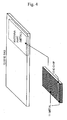
- Fig. 5 shows an example of the arrangement where the RFID tag of the present invention and a 13 MHz band RFID tag are stacked.
- Fig. 6 is a diagram showing the configuration of an exemplary embodiment of an antenna of the present invention in which the length of the loop is increased.
- Fig. 7 is a diagram showing an example of the matching characteristics of an antenna and IC chip of the present invention.
- Fig. 8 is a diagram showing an example of the direction of the electrical current flowing on the metal member in Figure 6 (b).
- Fig. 9 is a diagram showing an example of the configuration of an embodiment of an antenna which is a variation of the antenna configuration of Figure 6.
- Fig. 10 is a diagram showing an example of the matching characteristics of the third antenna and IC chip of the present invention.
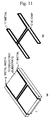
- Fig. 11 is a diagram showing an example of the configuration of a folded loop antenna which is a fourth antenna of the present invention.
- Fig. 12 is a diagram showing an example of the matching characteristics of the fourth antenna and IC chip of the present invention.
- Figure 3 shows the configurations of a plate-form loop antenna according to the present invention.
- a metal part 11 the surface of which is partially cut-out is wrapped on a dielectric substrate 10, and the power supply position and mounting position of an IC chip 12 are shown in the vicinity of the cut-out portion.
- Figure 4 shows an example of the layout of a plate-form loop antenna in an RFID tag of the present invention.
- Figure 4 the plate-form loop antenna of Figure 3 is placed inside the RFID tag 13 near the end thereof.
- Figure 5 shows an example of the arrangement whereby a 13 MHz band RFID tag is superposed on the RFID of the present invention.
- Figure 5 (a) is a block diagram showing a lateral view
- Figure 5 (b) is a block diagram showing a view from directly above.
- FIGs 5 (a) and (b) assume that a 13 MHz band RFID tag 20 and the RFID tag 13 have been stacked, and the antenna part (metal) held in the RFID tag 13 is arranged at one end thereof.
- a current is produced in the loop by passing magnetic flux produced by radio waves from the reader-writer inside the coiled loop antenna 21, and communication with the reader-writer is enabled on the basis of this current.
- the present invention is designed in such a way that, by reducing the antenna part (metal) in size and housing it inside the end part, the inside of this loop antenna 21 is not completely covered by the metal of the antenna, so as to avoid accepting the magnetic flux passing through the interior of the coiled loop antenna 21, as shown in Figures 5 (a) and (b).
- the RFID tag 13 of the present invention is constituted so that a magnetic flux region that is linked to the interior of the coiled loop antenna 21 can be secured, and the problem of failure of operation of the 13 MHz band RFID tag, as has occurred in the past, is solved.
- the reader-writer is sufficiently able to read information on the 13 MHz band RFID tag even if a 13 MHz band RFID tag and the RFID tag of the present invention are superposed.
- Figure 6 shows exemplary configurations of an antenna in which the length of the loop in the present invention is increased.
- the metal portion of the plate form loop antenna of Figure 3 is removed and the dielectric substrate exposed, so that the coiled loop antenna of the 13 MHz band RFID tag is not affected even if a 13 MHz band RFID tag is superposed thereon.
- Figure 6 (b) is a view which shows only the metallic part of the antenna configuration of Figure 6 (a).
- the antenna in Figure 6 is housed in the end part of the RFID tag in the same way as in Figure 5.
- the chip admittance is about 1 mS in the real part and 10 mS or above in the imaginary part.
- An antenna configuration and IC chip of this type have characteristics similar to those shown in Figure 7.
- the vertical axis for these characteristics is matching (VSWR), and the horizontal axis shows the frequency.
- the diagram in Figure 8 shows the direction of the electrical current passing over the metal is seen from the upper face of Figure 6 (b).
- the starting point from which the current flows is the IC chip mounting position.
- Figure 9 shows a third antenna configuration which is a variation of the antenna configuration shown in Figure 6.
- Figure 9 (a) shows the configuration in which the front and back of the dielectric substrate is covered with a cut-out metal part, and the respective metal parts form a loop as metallic wiring.
- the antenna in Figure 9 also is housed in the end part of the RFID tag as in Figure 5.
- the chip admittance is about 1 mS in the real part and 5 mS or above in the imaginary part.
- An antenna configuration and IC chip of this type have characteristics similar to those shown in Figure 10.
- Figure 11 shows the configuration of a folded loop antenna which is the fourth antenna of the present invention.
- the antenna in Figure 11 is housed in the end of the RFID tag as in Figure 5.
- the chip admittance is about 1 mS in the real part and 5 mS or above in the imaginary part.
- An antenna configuration and IC chip of this type have characteristics similar to those shown in Figure 12.
Landscapes
- Engineering & Computer Science (AREA)
- Computer Hardware Design (AREA)
- Microelectronics & Electronic Packaging (AREA)
- Physics & Mathematics (AREA)
- General Physics & Mathematics (AREA)
- Theoretical Computer Science (AREA)
- Computer Networks & Wireless Communication (AREA)
- Details Of Aerials (AREA)
- Support Of Aerials (AREA)
- Aerials With Secondary Devices (AREA)
- Near-Field Transmission Systems (AREA)
- Credit Cards Or The Like (AREA)
Applications Claiming Priority (1)
| Application Number | Priority Date | Filing Date | Title |
|---|---|---|---|
| JP2004313061A JP4333555B2 (ja) | 2004-10-27 | 2004-10-27 | Rfidタグ |
Publications (3)
| Publication Number | Publication Date |
|---|---|
| EP1653396A2 true EP1653396A2 (de) | 2006-05-03 |
| EP1653396A3 EP1653396A3 (de) | 2008-06-11 |
| EP1653396B1 EP1653396B1 (de) | 2011-08-31 |
Family
ID=35615597
Family Applications (1)
| Application Number | Title | Priority Date | Filing Date |
|---|---|---|---|
| EP05001594A Not-in-force EP1653396B1 (de) | 2004-10-27 | 2005-01-26 | RFID Etikette |
Country Status (6)
| Country | Link |
|---|---|
| US (1) | US7323994B2 (de) |
| EP (1) | EP1653396B1 (de) |
| JP (1) | JP4333555B2 (de) |
| KR (1) | KR100705524B1 (de) |
| CN (1) | CN100343870C (de) |
| TW (1) | TWI270012B (de) |
Families Citing this family (25)
| Publication number | Priority date | Publication date | Assignee | Title |
|---|---|---|---|---|
| US8436780B2 (en) * | 2010-07-12 | 2013-05-07 | Q-Track Corporation | Planar loop antenna system |
| JP4717830B2 (ja) | 2005-01-07 | 2011-07-06 | 富士通株式会社 | タグ装置 |
| WO2007000578A2 (en) | 2005-06-25 | 2007-01-04 | Omni-Id Limited | Electromagnetic radiation decoupler |
| JP4208254B2 (ja) * | 2006-05-31 | 2009-01-14 | サンコール株式会社 | アンテナユニット,無線通信構造体及びアンテナ構造 |
| US7659821B2 (en) * | 2006-09-14 | 2010-02-09 | International Business Machines Corporation | Smart radio-frequency identification (RFID) infrastructure and method |
| US20080174380A1 (en) * | 2006-10-17 | 2008-07-24 | Powerid Ltd. | Method and circuit for providing rf isolation of a power source and an rf device employing such a circuit |
| US8162230B2 (en) * | 2006-10-17 | 2012-04-24 | Powerid Ltd. | Method and circuit for providing RF isolation of a power source from an antenna and an RFID device employing such a circuit |
| JP2008113632A (ja) * | 2006-11-07 | 2008-05-22 | Hitachi Ltd | 生体植込用rfidタグおよびその挿入冶具体 |
| US20080180254A1 (en) * | 2007-01-31 | 2008-07-31 | Kajander John A | Circularly-polarized rfid tag antenna structure |
| JP4894923B2 (ja) * | 2007-06-29 | 2012-03-14 | 富士通株式会社 | ループアンテナ |
| US20100265041A1 (en) * | 2009-04-16 | 2010-10-21 | Powerid Ltd. | Rfid transponder |
| CN101853413B (zh) * | 2010-03-12 | 2014-09-17 | 北京创毅视讯科技有限公司 | 一种应用于物联网的电子标签及使用该电子标签的系统 |
| EP2372598B1 (de) * | 2010-03-15 | 2012-12-12 | Nxp B.V. | Etikettkommunikationsvorrichtungen |
| KR20140117614A (ko) * | 2012-01-23 | 2014-10-07 | 페이닉스 아마테크 테오란타 | 금속증착 스마트 카드의 차폐현상 보상 및 커플링 개선 |
| US8922443B2 (en) * | 2012-09-27 | 2014-12-30 | Apple Inc. | Distributed loop antenna with multiple subloops |
| CN103617442A (zh) * | 2013-11-21 | 2014-03-05 | 高洪强 | 一种盒体uhf-rfid电子标签 |
| CN104021416A (zh) * | 2014-06-27 | 2014-09-03 | 南通富士通微电子股份有限公司 | 电子标签 |
| KR101619322B1 (ko) * | 2015-01-05 | 2016-05-10 | 주식회사 아모텍 | 메탈 케이스를 이용한 nfc 안테나 모듈 |
| US10591592B2 (en) | 2015-06-15 | 2020-03-17 | Humatics Corporation | High-precision time of flight measurement systems |
| US9805229B2 (en) * | 2015-10-15 | 2017-10-31 | International Business Machines Corporation | Location sensing using a radio frequency tag |
| CN108701896B (zh) * | 2015-12-17 | 2021-03-12 | 修麦提克斯公司 | 用于实现射频定位的装置 |
| WO2017219233A1 (en) | 2016-06-21 | 2017-12-28 | 3M Innovative Properties Company | Self-supporting antenna |
| CN106845609A (zh) * | 2017-01-05 | 2017-06-13 | 上扬无线射频科技扬州有限公司 | 具有群读功能高频点rfid标签 |
| US12080415B2 (en) | 2020-10-09 | 2024-09-03 | Humatics Corporation | Radio-frequency systems and methods for co-localization of medical devices and patients |
| WO2024079663A1 (en) * | 2022-10-12 | 2024-04-18 | Avery Dennison Retail Information Services Llc | Wideband non-folded on-metal uhf rfid tag |
Citations (4)
| Publication number | Priority date | Publication date | Assignee | Title |
|---|---|---|---|---|
| JPH0888586A (ja) | 1994-09-09 | 1996-04-02 | Internatl Business Mach Corp <Ibm> | 薄型フレキシブル無線周波数タグ回路 |
| WO2000054216A1 (de) | 1999-03-10 | 2000-09-14 | Skidata Ag | Nichtübertragbarer berechtigungsausweis |
| JP2002353735A (ja) | 2001-05-25 | 2002-12-06 | Sharp Corp | 無線通信装置 |
| EP1298578A1 (de) | 2001-01-26 | 2003-04-02 | Sony Corporation | Kontaktlose chipkarte |
Family Cites Families (10)
| Publication number | Priority date | Publication date | Assignee | Title |
|---|---|---|---|---|
| CH684661A5 (de) * | 1992-12-11 | 1994-11-15 | Kobe Properties Ltd | Verfahren und Vorrichtung zur Diebstahlsicherung von Gegenständen. |
| US5751256A (en) * | 1994-03-04 | 1998-05-12 | Flexcon Company Inc. | Resonant tag labels and method of making same |
| US5682143A (en) * | 1994-09-09 | 1997-10-28 | International Business Machines Corporation | Radio frequency identification tag |
| US6411213B1 (en) * | 1995-10-11 | 2002-06-25 | Motorola, Inc. | Radio frequency identification tag system using tags arranged for coupling to ground |
| US6840440B2 (en) * | 1998-11-11 | 2005-01-11 | Mitsubishi Materials Corporation | Identifying system of overlapped tag |
| US6451154B1 (en) * | 2000-02-18 | 2002-09-17 | Moore North America, Inc. | RFID manufacturing concepts |
| MXPA03001220A (es) * | 2000-08-11 | 2003-05-27 | Escort Memory Systems | Conjunto y sistema de marbete de identificacion de radiofrecuencia. |
| DE10393263T5 (de) * | 2002-09-20 | 2005-09-15 | Fairchild Semiconductor Corp. | Verfahren und System für eine logarithmische Wendelantenne mit großer Bandbreite für ein Radio- frequenzidentifizierungskennzeichnungssystem |
| EP1416585B1 (de) * | 2002-10-31 | 2009-02-11 | Sony Ericsson Mobile Communications AB | Breitbandige Loop-Antenne |
| US6999028B2 (en) * | 2003-12-23 | 2006-02-14 | 3M Innovative Properties Company | Ultra high frequency radio frequency identification tag |
-
2004
- 2004-10-27 JP JP2004313061A patent/JP4333555B2/ja not_active Expired - Fee Related
-
2005
- 2005-01-18 US US11/035,734 patent/US7323994B2/en not_active Expired - Fee Related
- 2005-01-19 TW TW094101518A patent/TWI270012B/zh not_active IP Right Cessation
- 2005-01-26 EP EP05001594A patent/EP1653396B1/de not_active Not-in-force
- 2005-02-14 KR KR1020050011827A patent/KR100705524B1/ko not_active IP Right Cessation
- 2005-02-18 CN CNB2005100085138A patent/CN100343870C/zh not_active Expired - Fee Related
Patent Citations (4)
| Publication number | Priority date | Publication date | Assignee | Title |
|---|---|---|---|---|
| JPH0888586A (ja) | 1994-09-09 | 1996-04-02 | Internatl Business Mach Corp <Ibm> | 薄型フレキシブル無線周波数タグ回路 |
| WO2000054216A1 (de) | 1999-03-10 | 2000-09-14 | Skidata Ag | Nichtübertragbarer berechtigungsausweis |
| EP1298578A1 (de) | 2001-01-26 | 2003-04-02 | Sony Corporation | Kontaktlose chipkarte |
| JP2002353735A (ja) | 2001-05-25 | 2002-12-06 | Sharp Corp | 無線通信装置 |
Also Published As
| Publication number | Publication date |
|---|---|
| JP2006128953A (ja) | 2006-05-18 |
| TWI270012B (en) | 2007-01-01 |
| KR100705524B1 (ko) | 2007-04-10 |
| JP4333555B2 (ja) | 2009-09-16 |
| US7323994B2 (en) | 2008-01-29 |
| TW200614085A (en) | 2006-05-01 |
| CN1766913A (zh) | 2006-05-03 |
| EP1653396B1 (de) | 2011-08-31 |
| EP1653396A3 (de) | 2008-06-11 |
| US20060097058A1 (en) | 2006-05-11 |
| KR20060041908A (ko) | 2006-05-12 |
| CN100343870C (zh) | 2007-10-17 |
Similar Documents
| Publication | Publication Date | Title |
|---|---|---|
| US7323994B2 (en) | RFID tag | |
| US10062956B2 (en) | Antenna device and electronic apparatus | |
| JP4393228B2 (ja) | 小型アンテナ及びそれを備えた無線タグ | |
| US6970135B2 (en) | Antenna apparatus | |
| US7416135B2 (en) | IC tag and IC tag attachment structure | |
| KR100817395B1 (ko) | 절첩 다이폴 안테나 및 이것을 사용한 태그 | |
| EP2071495B1 (de) | Drahtloses gerät mit integriertem schaltkreis | |
| US20080143620A1 (en) | Increasing the bandwidth of a RFID dipole tag | |
| US20090140947A1 (en) | Antenna Device and Radio-Communication System Using the Same | |
| US8400362B2 (en) | Radio communication apparatus and method for making radio communication apparatus | |
| JP2009516413A (ja) | 無線周波数識別システムのトランスポンダ用広帯域アンテナ | |
| US20100007567A1 (en) | Antenna for an rfid transponder and rfid transponder | |
| US11625568B2 (en) | Flexible mountable L-shaped RFID tag antenna | |
| CN109219906A (zh) | 天线装置 | |
| US7378972B2 (en) | RFID tag | |
| KR101014624B1 (ko) | 다중대역에서 동작하는 안테나 모듈 및 상기 안테나 모듈을포함하는 통신 시스템 | |
| JP2011009903A (ja) | 磁性体アンテナ及びアンテナ装置 | |
| KR100848560B1 (ko) | 무접지면 평면 안테나 | |
| KR20070009892A (ko) | 등방성 복사패턴을 갖는 광대역 안테나 | |
| JP4479765B2 (ja) | Rfidタグ | |
| JP5708193B2 (ja) | アンテナ装置 | |
| KR20130065895A (ko) | 안테나 및 이를 포함하는 무선인식용 태그 | |
| JP2001168618A (ja) | 無接触形icカードシステムにおけるリードライタ用のアンテナ装置 |
Legal Events
| Date | Code | Title | Description |
|---|---|---|---|
| PUAI | Public reference made under article 153(3) epc to a published international application that has entered the european phase |
Free format text: ORIGINAL CODE: 0009012 |
|
| AK | Designated contracting states |
Kind code of ref document: A2 Designated state(s): AT BE BG CH CY CZ DE DK EE ES FI FR GB GR HU IE IS IT LI LT LU MC NL PL PT RO SE SI SK TR |
|
| AX | Request for extension of the european patent |
Extension state: AL BA HR LV MK YU |
|
| PUAL | Search report despatched |
Free format text: ORIGINAL CODE: 0009013 |
|
| AK | Designated contracting states |
Kind code of ref document: A3 Designated state(s): AT BE BG CH CY CZ DE DK EE ES FI FR GB GR HU IE IS IT LI LT LU MC NL PL PT RO SE SI SK TR |
|
| AX | Request for extension of the european patent |
Extension state: AL BA HR LV MK YU |
|
| RIC1 | Information provided on ipc code assigned before grant |
Ipc: G06K 19/077 20060101AFI20060127BHEP Ipc: H01Q 1/22 20060101ALI20080502BHEP |
|
| 17P | Request for examination filed |
Effective date: 20080709 |
|
| 17Q | First examination report despatched |
Effective date: 20081010 |
|
| AKX | Designation fees paid |
Designated state(s): DE FR GB |
|
| GRAP | Despatch of communication of intention to grant a patent |
Free format text: ORIGINAL CODE: EPIDOSNIGR1 |
|
| GRAS | Grant fee paid |
Free format text: ORIGINAL CODE: EPIDOSNIGR3 |
|
| GRAA | (expected) grant |
Free format text: ORIGINAL CODE: 0009210 |
|
| AK | Designated contracting states |
Kind code of ref document: B1 Designated state(s): DE FR GB |
|
| REG | Reference to a national code |
Ref country code: GB Ref legal event code: FG4D |
|
| REG | Reference to a national code |
Ref country code: DE Ref legal event code: R096 Ref document number: 602005029823 Country of ref document: DE Effective date: 20111124 |
|
| PLBE | No opposition filed within time limit |
Free format text: ORIGINAL CODE: 0009261 |
|
| STAA | Information on the status of an ep patent application or granted ep patent |
Free format text: STATUS: NO OPPOSITION FILED WITHIN TIME LIMIT |
|
| 26N | No opposition filed |
Effective date: 20120601 |
|
| REG | Reference to a national code |
Ref country code: DE Ref legal event code: R097 Ref document number: 602005029823 Country of ref document: DE Effective date: 20120601 |
|
| REG | Reference to a national code |
Ref country code: FR Ref legal event code: PLFP Year of fee payment: 11 |
|
| PGFP | Annual fee paid to national office [announced via postgrant information from national office to epo] |
Ref country code: DE Payment date: 20150120 Year of fee payment: 11 |
|
| PGFP | Annual fee paid to national office [announced via postgrant information from national office to epo] |
Ref country code: FR Payment date: 20150108 Year of fee payment: 11 Ref country code: GB Payment date: 20150121 Year of fee payment: 11 |
|
| REG | Reference to a national code |
Ref country code: DE Ref legal event code: R119 Ref document number: 602005029823 Country of ref document: DE |
|
| GBPC | Gb: european patent ceased through non-payment of renewal fee |
Effective date: 20160126 |
|
| REG | Reference to a national code |
Ref country code: FR Ref legal event code: ST Effective date: 20160930 |
|
| PG25 | Lapsed in a contracting state [announced via postgrant information from national office to epo] |
Ref country code: GB Free format text: LAPSE BECAUSE OF NON-PAYMENT OF DUE FEES Effective date: 20160126 Ref country code: DE Free format text: LAPSE BECAUSE OF NON-PAYMENT OF DUE FEES Effective date: 20160802 |
|
| PG25 | Lapsed in a contracting state [announced via postgrant information from national office to epo] |
Ref country code: FR Free format text: LAPSE BECAUSE OF NON-PAYMENT OF DUE FEES Effective date: 20160201 |