EP1652292B1 - Offset correction for down-conversion mixers - Google Patents
Offset correction for down-conversion mixers Download PDFInfo
- Publication number
- EP1652292B1 EP1652292B1 EP03817621A EP03817621A EP1652292B1 EP 1652292 B1 EP1652292 B1 EP 1652292B1 EP 03817621 A EP03817621 A EP 03817621A EP 03817621 A EP03817621 A EP 03817621A EP 1652292 B1 EP1652292 B1 EP 1652292B1
- Authority
- EP
- European Patent Office
- Prior art keywords
- signal
- phase
- differential
- imbalance
- peak
- Prior art date
- Legal status (The legal status is an assumption and is not a legal conclusion. Google has not performed a legal analysis and makes no representation as to the accuracy of the status listed.)
- Expired - Lifetime
Links
- 238000006243 chemical reaction Methods 0.000 title claims abstract description 25
- 238000012937 correction Methods 0.000 title claims abstract description 23
- 238000000034 method Methods 0.000 claims description 6
- 230000001419 dependent effect Effects 0.000 claims 5
- 230000000295 complement effect Effects 0.000 description 5
- 230000000875 corresponding effect Effects 0.000 description 3
- 238000004891 communication Methods 0.000 description 2
- 230000000644 propagated effect Effects 0.000 description 2
- 239000003990 capacitor Substances 0.000 description 1
- 230000001413 cellular effect Effects 0.000 description 1
- 230000002596 correlated effect Effects 0.000 description 1
- 238000010168 coupling process Methods 0.000 description 1
- 238000005859 coupling reaction Methods 0.000 description 1
- 238000013461 design Methods 0.000 description 1
- 230000000694 effects Effects 0.000 description 1
- 238000012545 processing Methods 0.000 description 1
- 230000035945 sensitivity Effects 0.000 description 1
Images
Classifications
-
- H—ELECTRICITY
- H03—ELECTRONIC CIRCUITRY
- H03D—DEMODULATION OR TRANSFERENCE OF MODULATION FROM ONE CARRIER TO ANOTHER
- H03D7/00—Transference of modulation from one carrier to another, e.g. frequency-changing
- H03D7/14—Balanced arrangements
- H03D7/1425—Balanced arrangements with transistors
- H03D7/1433—Balanced arrangements with transistors using bipolar transistors
-
- H—ELECTRICITY
- H03—ELECTRONIC CIRCUITRY
- H03D—DEMODULATION OR TRANSFERENCE OF MODULATION FROM ONE CARRIER TO ANOTHER
- H03D7/00—Transference of modulation from one carrier to another, e.g. frequency-changing
- H03D7/14—Balanced arrangements
- H03D7/1425—Balanced arrangements with transistors
-
- H—ELECTRICITY
- H03—ELECTRONIC CIRCUITRY
- H03D—DEMODULATION OR TRANSFERENCE OF MODULATION FROM ONE CARRIER TO ANOTHER
- H03D7/00—Transference of modulation from one carrier to another, e.g. frequency-changing
- H03D7/14—Balanced arrangements
- H03D7/1425—Balanced arrangements with transistors
- H03D7/1441—Balanced arrangements with transistors using field-effect transistors
-
- H—ELECTRICITY
- H03—ELECTRONIC CIRCUITRY
- H03D—DEMODULATION OR TRANSFERENCE OF MODULATION FROM ONE CARRIER TO ANOTHER
- H03D7/00—Transference of modulation from one carrier to another, e.g. frequency-changing
- H03D7/14—Balanced arrangements
- H03D7/1425—Balanced arrangements with transistors
- H03D7/1458—Double balanced arrangements, i.e. where both input signals are differential
-
- H—ELECTRICITY
- H03—ELECTRONIC CIRCUITRY
- H03D—DEMODULATION OR TRANSFERENCE OF MODULATION FROM ONE CARRIER TO ANOTHER
- H03D2200/00—Indexing scheme relating to details of demodulation or transference of modulation from one carrier to another covered by H03D
- H03D2200/0041—Functional aspects of demodulators
- H03D2200/0043—Bias and operating point
-
- H—ELECTRICITY
- H03—ELECTRONIC CIRCUITRY
- H03D—DEMODULATION OR TRANSFERENCE OF MODULATION FROM ONE CARRIER TO ANOTHER
- H03D2200/00—Indexing scheme relating to details of demodulation or transference of modulation from one carrier to another covered by H03D
- H03D2200/0041—Functional aspects of demodulators
- H03D2200/0047—Offset of DC voltage or frequency
-
- H—ELECTRICITY
- H03—ELECTRONIC CIRCUITRY
- H03D—DEMODULATION OR TRANSFERENCE OF MODULATION FROM ONE CARRIER TO ANOTHER
- H03D2200/00—Indexing scheme relating to details of demodulation or transference of modulation from one carrier to another covered by H03D
- H03D2200/0041—Functional aspects of demodulators
- H03D2200/009—Reduction of local oscillator or RF leakage
Definitions
- This invention relates to the field of communications, and in particular to a switching and bias correction system for direct conversion receivers.
- Direct conversion receivers are commonly used in wireless communication devices, such as cellular telephones.
- a particular concern in the design of such devices is the interference that each device may cause to each other device in a local environment.
- LO local oscillator
- RF radio-frequency
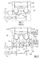
- FIG. 1 illustrates an example schematic of a prior art direct conversion receiver system 100.
- a mixer 150 demodulates an RF signal 110 via a local oscillator 120 to produce a baseband output Vout.
- the complementary outputs of the local oscillator 120 are true inversions of each other, if the transistors and load resistors are matched, and if the input transconductance is ideally balanced, there will be no leakage of the local oscillator 120 into the RF signal 110.
- differential circuits are used throughout, thereby cancelling the common-mode leakage or noise.
- the switching points of the transistors in the mixer 150 will differ, and a difference signal at the local oscillator frequency will be created.
- this difference signal is a common-mode signal
- an imbalance of the input transconductance at the tail nodes 151, 152 will transform this common-mode signal to a differential-mode signal, which will be propagated back to the RF signal 110, and possibly emanated from the RF antenna at the local oscillator frequency.
- US-A-2002/0097081 describes a circuit in which a transconductance amplifier having a programmable gain is coupled to the output of a mixer in a feedback loop for reducing DC offset.
- a direct conversion receiver that includes a detector that provides a measure of bias offset that is caused by component mismatches in the direct conversion mixer, and a corrective network that reduces the bias offset based on this measure.
- the direct conversion mixer demodulates a radio-frequency (RF) input signal via mixing with a local-oscillator (LO) signal to provide a differential baseband output signal.
- RF radio-frequency
- LO local-oscillator
- a differential peak detector compares the peak signal value at each side of the mixer's differential output, and a differential integrator averages the difference between these peak signal values to provide the measure of bias offset.
- the corrective network adds a correction offset to each of the local oscillator local oscillator paths on each of the switching pairs that provide the differential output, but opposite to the local oscillator connections.
- Fig. 2 illustrates an example schematic of a direct conversion receiver 200 with bias-offset correction in accordance with this invention.
- the receiver 200 includes a mixer 250, corresponding to the mixer 150 of the prior art Fig. 1 , with the addition of a corrective network 240 that adjusts the bias levels of the mixing transistors T1A, T1B, T2A, and T2B to minimize the effects of component variations in the mixer 250.
- the input RF signal is alternately mixed with symmetric half-cycles of the local oscillator, each half cycle being processed by alternate transistors in each differential branch of the mixer.
- each side, or phase, VoutA and VoutB, of the differential voltage output Vout will exhibit equal and opposite signal excursions about a common DC level.
- Component variations in the mixer that affect the bias of the transistors will shift the crossover points in the individual transistor pairs, and cause an imbalance within the transistor pair and/or between the transistor pairs.
- imbalance is used hereinafter to refer to responses that differ from the symmetric responses of an ideal mixer.
- This invention is premised on the observation that imbalances caused by component variations in a mixer cause an imbalance between the phases of the differential output of a direct conversion mixer, and a measure of the imbalance at the differential output can be used to correct the mixer for such imbalances.
- a bias-error detector 230 detects the imbalance within the opposing phases VoutA and VoutB of the differential output Vout.
- the detected imbalance is provided to a bias error corrector 245 in the corrective network 240, to provide correction signals CA and CB for adjusting the bias of each of the transistors T1A, T1B, T2A, and T2B.
- correction signals CA and CB are directly correlated to the imbalance of VoutA and VoutB, respectively.
- the correction signals CA, CB are applied in opposition to the local oscillator 120. That is, correction signal CA is applied to transistors T1B and T2B, to affect VoutB, and correction signal CB is applied to transistors T1A and T2A, to affect VoutA.
- correction signal CA is applied to transistors T1B and T2B, to affect VoutB
- correction signal CB is applied to transistors T1A and T2A, to affect VoutA.
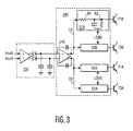
- FIG. 3 illustrates an example schematic of a bias error detector 230 and corrective network 240 in accordance with this invention, although other techniques for detecting an imbalance within and between each phase of a differential output pair, VoutA and VoutB, and for providing a correction signal CA, CB to the mixer 250 to compensate for the imbalance will be evident to one of ordinary skill in the art in view of this disclosure.
- the example bias error detector 230 comprises a differential amplifier, to eliminate the common DC potential of the differential output pair, followed by a pair of rectifier-capacitors, to form a peak-detector pair for measuring the peak excursion of each phase of the differential output pair relative to the common DC potential.
- the corrective network 240 includes a differential integrator 245 that averages the differences between the peak values to produce the correction values CA, CB.
- the summing devices S1A, S1B, S2A, and S2B add the correction values CB, CA to the opposing local oscillator signals LO(A), LO(B) to adjust the bias of the corresponding transistors T1A, T1B, S2A, and S2B, respectively.
- FIG. 3 also illustrates an example summing device S1B.
- the correction signal is applied via a large resistor R1, relative to a smaller resistor R2 in the local oscillator path.
- the resistor R2 sets the common-mode bias, while the resistor R1 modifies the bias based on the unbalance between the phases of the differential output Vout.
- the local oscillator is also capacitively coupled to the mixing transistor.
Landscapes
- Engineering & Computer Science (AREA)
- Power Engineering (AREA)
- Superheterodyne Receivers (AREA)
- Radar Systems Or Details Thereof (AREA)
Applications Claiming Priority (1)
| Application Number | Priority Date | Filing Date | Title |
|---|---|---|---|
| PCT/IB2003/003362 WO2005011103A1 (en) | 2003-07-25 | 2003-07-25 | Offset correction for down-conversion mixers |
Publications (2)
| Publication Number | Publication Date |
|---|---|
| EP1652292A1 EP1652292A1 (en) | 2006-05-03 |
| EP1652292B1 true EP1652292B1 (en) | 2008-10-15 |
Family
ID=34090440
Family Applications (1)
| Application Number | Title | Priority Date | Filing Date |
|---|---|---|---|
| EP03817621A Expired - Lifetime EP1652292B1 (en) | 2003-07-25 | 2003-07-25 | Offset correction for down-conversion mixers |
Country Status (7)
| Country | Link |
|---|---|
| EP (1) | EP1652292B1 (cg-RX-API-DMAC7.html) |
| JP (1) | JP4466870B2 (cg-RX-API-DMAC7.html) |
| CN (1) | CN100576721C (cg-RX-API-DMAC7.html) |
| AT (1) | ATE411641T1 (cg-RX-API-DMAC7.html) |
| AU (1) | AU2003255876A1 (cg-RX-API-DMAC7.html) |
| DE (1) | DE60324204D1 (cg-RX-API-DMAC7.html) |
| WO (1) | WO2005011103A1 (cg-RX-API-DMAC7.html) |
Cited By (1)
| Publication number | Priority date | Publication date | Assignee | Title |
|---|---|---|---|---|
| WO2024263382A1 (en) * | 2023-06-23 | 2024-12-26 | Qualcomm Incorporated | Active mixers with enhanced image rejection ratio (irr) |
Families Citing this family (8)
| Publication number | Priority date | Publication date | Assignee | Title |
|---|---|---|---|---|
| JP2006314029A (ja) * | 2005-05-09 | 2006-11-16 | Renesas Technology Corp | 無線通信用半導体集積回路装置 |
| DE102005028747B4 (de) | 2005-06-21 | 2010-12-16 | Infineon Technologies Ag | Mischeranordnung, Verwendung der Mischeranordnung und Verfahren zur Frequenzumsetzung |
| DE102006018309A1 (de) * | 2006-04-20 | 2007-10-25 | Hella Kgaa Hueck & Co. | Vorrichtung zum Entstören von kleinen Signalen |
| US8515362B2 (en) * | 2008-10-30 | 2013-08-20 | Qualcomm, Incorporated | Mixer architectures |
| JP5853881B2 (ja) * | 2012-06-26 | 2016-02-09 | 三菱電機株式会社 | 無線通信装置 |
| US8847662B2 (en) * | 2012-09-11 | 2014-09-30 | Mediatek Inc. | Mixer and associated signal circuit |
| US9948239B2 (en) | 2016-09-21 | 2018-04-17 | Qualcomm Incorporated | Configurable mixer |
| US10193497B2 (en) * | 2016-12-06 | 2019-01-29 | Qualcomm Incorporated | Enhanced broadband operation of an active mixer |
Family Cites Families (4)
| Publication number | Priority date | Publication date | Assignee | Title |
|---|---|---|---|---|
| US5933771A (en) * | 1997-06-20 | 1999-08-03 | Nortel Networks Corporation | Low voltage gain controlled mixer |
| JP2002111412A (ja) * | 2000-09-29 | 2002-04-12 | Toshiba Corp | 増幅回路 |
| US6509777B2 (en) * | 2001-01-23 | 2003-01-21 | Resonext Communications, Inc. | Method and apparatus for reducing DC offset |
| WO2002084859A1 (en) * | 2001-04-18 | 2002-10-24 | Nokia Corporation | Balanced circuit arrangement and method for linearizing such an arrangement |
-
2003
- 2003-07-25 DE DE60324204T patent/DE60324204D1/de not_active Expired - Lifetime
- 2003-07-25 AT AT03817621T patent/ATE411641T1/de not_active IP Right Cessation
- 2003-07-25 JP JP2005504543A patent/JP4466870B2/ja not_active Expired - Fee Related
- 2003-07-25 CN CN03826838.8A patent/CN100576721C/zh not_active Expired - Fee Related
- 2003-07-25 EP EP03817621A patent/EP1652292B1/en not_active Expired - Lifetime
- 2003-07-25 WO PCT/IB2003/003362 patent/WO2005011103A1/en not_active Ceased
- 2003-07-25 AU AU2003255876A patent/AU2003255876A1/en not_active Abandoned
Cited By (2)
| Publication number | Priority date | Publication date | Assignee | Title |
|---|---|---|---|---|
| WO2024263382A1 (en) * | 2023-06-23 | 2024-12-26 | Qualcomm Incorporated | Active mixers with enhanced image rejection ratio (irr) |
| US12463592B2 (en) | 2023-06-23 | 2025-11-04 | Qualcomm Incorporated | Active mixers with enhanced image rejection ratio (IRR) |
Also Published As
| Publication number | Publication date |
|---|---|
| ATE411641T1 (de) | 2008-10-15 |
| CN100576721C (zh) | 2009-12-30 |
| EP1652292A1 (en) | 2006-05-03 |
| JP4466870B2 (ja) | 2010-05-26 |
| DE60324204D1 (cg-RX-API-DMAC7.html) | 2008-11-27 |
| CN1802785A (zh) | 2006-07-12 |
| AU2003255876A1 (en) | 2005-02-14 |
| WO2005011103A1 (en) | 2005-02-03 |
| JP2007516624A (ja) | 2007-06-21 |
Similar Documents
| Publication | Publication Date | Title |
|---|---|---|
| US8676145B2 (en) | Mixer circuits for second order intercept point calibration | |
| US7536165B2 (en) | Offset correction for down-conversion mixers | |
| CN1728694B (zh) | Rf接收机失配校准系统和方法 | |
| US7236761B2 (en) | Balanced circuit arrangement and method for linearizing such an arrangement | |
| JP3721144B2 (ja) | 周波数変換器、直交復調器及び直交変調器 | |
| CN1639992B (zh) | 降低失真的校准的装置和方法 | |
| CN108540240B (zh) | 用于校准射频发射器以补偿共模本地振荡器泄漏的装置和方法 | |
| EP1560326A1 (en) | Mixer circuit for direct conversion transceiver with improved second intermodulation product | |
| WO2003005562A2 (en) | Radio receiver using a feedback loop to compensate i/q amplitude errors, and method | |
| Kivekas et al. | Calibration techniques of active BiCMOS mixers | |
| CN111404489B (zh) | 混频器偏压电路 | |
| US7266357B2 (en) | Reduced local oscillator feedthrough quadrature image reject mixer | |
| EP1652292B1 (en) | Offset correction for down-conversion mixers | |
| US20120243641A1 (en) | Quadrature signal phase controller for controlling phase | |
| US7949324B2 (en) | Method for compensating transmission carrier leakage and transceiving circuit embodying the same | |
| JP4826960B2 (ja) | 負荷インピーダンスの較正手段を備えた平衡形ミクサ | |
| JP5429191B2 (ja) | 受信装置、イメージ信号の減衰方法及びミスマッチ補償方法 | |
| US12463592B2 (en) | Active mixers with enhanced image rejection ratio (IRR) | |
| US12273132B2 (en) | Spurious emissions detection and calibration using envelope detector | |
| JP3545615B2 (ja) | 無線受信装置 | |
| JP2025017743A (ja) | Rf送信機 | |
| JP2001223535A (ja) | 半導体装置およびその検査方法 |
Legal Events
| Date | Code | Title | Description |
|---|---|---|---|
| PUAI | Public reference made under article 153(3) epc to a published international application that has entered the european phase |
Free format text: ORIGINAL CODE: 0009012 |
|
| 17P | Request for examination filed |
Effective date: 20060227 |
|
| AK | Designated contracting states |
Kind code of ref document: A1 Designated state(s): AT BE BG CH CY CZ DE DK EE ES FI FR GB GR HU IE IT LI LU MC NL PT RO SE SI SK TR |
|
| 17Q | First examination report despatched |
Effective date: 20060906 |
|
| DAX | Request for extension of the european patent (deleted) | ||
| GRAP | Despatch of communication of intention to grant a patent |
Free format text: ORIGINAL CODE: EPIDOSNIGR1 |
|
| GRAS | Grant fee paid |
Free format text: ORIGINAL CODE: EPIDOSNIGR3 |
|
| GRAA | (expected) grant |
Free format text: ORIGINAL CODE: 0009210 |
|
| AK | Designated contracting states |
Kind code of ref document: B1 Designated state(s): AT BE BG CH CY CZ DE DK EE ES FI FR GB GR HU IE IT LI LU MC NL PT RO SE SI SK TR |
|
| REG | Reference to a national code |
Ref country code: GB Ref legal event code: FG4D Ref country code: CH Ref legal event code: EP |
|
| RAP2 | Party data changed (patent owner data changed or rights of a patent transferred) |
Owner name: NXP B.V. |
|
| REG | Reference to a national code |
Ref country code: IE Ref legal event code: FG4D |
|
| REF | Corresponds to: |
Ref document number: 60324204 Country of ref document: DE Date of ref document: 20081127 Kind code of ref document: P |
|
| NLT2 | Nl: modifications (of names), taken from the european patent patent bulletin |
Owner name: NXP B.V. Effective date: 20081105 |
|
| NLV1 | Nl: lapsed or annulled due to failure to fulfill the requirements of art. 29p and 29m of the patents act | ||
| PG25 | Lapsed in a contracting state [announced via postgrant information from national office to epo] |
Ref country code: ES Free format text: LAPSE BECAUSE OF FAILURE TO SUBMIT A TRANSLATION OF THE DESCRIPTION OR TO PAY THE FEE WITHIN THE PRESCRIBED TIME-LIMIT Effective date: 20090126 Ref country code: BG Free format text: LAPSE BECAUSE OF FAILURE TO SUBMIT A TRANSLATION OF THE DESCRIPTION OR TO PAY THE FEE WITHIN THE PRESCRIBED TIME-LIMIT Effective date: 20090115 Ref country code: AT Free format text: LAPSE BECAUSE OF FAILURE TO SUBMIT A TRANSLATION OF THE DESCRIPTION OR TO PAY THE FEE WITHIN THE PRESCRIBED TIME-LIMIT Effective date: 20081015 |
|
| PG25 | Lapsed in a contracting state [announced via postgrant information from national office to epo] |
Ref country code: SI Free format text: LAPSE BECAUSE OF FAILURE TO SUBMIT A TRANSLATION OF THE DESCRIPTION OR TO PAY THE FEE WITHIN THE PRESCRIBED TIME-LIMIT Effective date: 20081015 Ref country code: PT Free format text: LAPSE BECAUSE OF FAILURE TO SUBMIT A TRANSLATION OF THE DESCRIPTION OR TO PAY THE FEE WITHIN THE PRESCRIBED TIME-LIMIT Effective date: 20090316 Ref country code: FI Free format text: LAPSE BECAUSE OF FAILURE TO SUBMIT A TRANSLATION OF THE DESCRIPTION OR TO PAY THE FEE WITHIN THE PRESCRIBED TIME-LIMIT Effective date: 20081015 Ref country code: NL Free format text: LAPSE BECAUSE OF FAILURE TO SUBMIT A TRANSLATION OF THE DESCRIPTION OR TO PAY THE FEE WITHIN THE PRESCRIBED TIME-LIMIT Effective date: 20081015 |
|
| PG25 | Lapsed in a contracting state [announced via postgrant information from national office to epo] |
Ref country code: BE Free format text: LAPSE BECAUSE OF FAILURE TO SUBMIT A TRANSLATION OF THE DESCRIPTION OR TO PAY THE FEE WITHIN THE PRESCRIBED TIME-LIMIT Effective date: 20081015 Ref country code: EE Free format text: LAPSE BECAUSE OF FAILURE TO SUBMIT A TRANSLATION OF THE DESCRIPTION OR TO PAY THE FEE WITHIN THE PRESCRIBED TIME-LIMIT Effective date: 20081015 Ref country code: DK Free format text: LAPSE BECAUSE OF FAILURE TO SUBMIT A TRANSLATION OF THE DESCRIPTION OR TO PAY THE FEE WITHIN THE PRESCRIBED TIME-LIMIT Effective date: 20081015 Ref country code: RO Free format text: LAPSE BECAUSE OF FAILURE TO SUBMIT A TRANSLATION OF THE DESCRIPTION OR TO PAY THE FEE WITHIN THE PRESCRIBED TIME-LIMIT Effective date: 20081015 |
|
| PLBE | No opposition filed within time limit |
Free format text: ORIGINAL CODE: 0009261 |
|
| STAA | Information on the status of an ep patent application or granted ep patent |
Free format text: STATUS: NO OPPOSITION FILED WITHIN TIME LIMIT |
|
| PG25 | Lapsed in a contracting state [announced via postgrant information from national office to epo] |
Ref country code: SE Free format text: LAPSE BECAUSE OF FAILURE TO SUBMIT A TRANSLATION OF THE DESCRIPTION OR TO PAY THE FEE WITHIN THE PRESCRIBED TIME-LIMIT Effective date: 20090115 Ref country code: IT Free format text: LAPSE BECAUSE OF FAILURE TO SUBMIT A TRANSLATION OF THE DESCRIPTION OR TO PAY THE FEE WITHIN THE PRESCRIBED TIME-LIMIT Effective date: 20081015 Ref country code: CZ Free format text: LAPSE BECAUSE OF FAILURE TO SUBMIT A TRANSLATION OF THE DESCRIPTION OR TO PAY THE FEE WITHIN THE PRESCRIBED TIME-LIMIT Effective date: 20081015 |
|
| 26N | No opposition filed |
Effective date: 20090716 |
|
| PG25 | Lapsed in a contracting state [announced via postgrant information from national office to epo] |
Ref country code: SK Free format text: LAPSE BECAUSE OF FAILURE TO SUBMIT A TRANSLATION OF THE DESCRIPTION OR TO PAY THE FEE WITHIN THE PRESCRIBED TIME-LIMIT Effective date: 20081015 |
|
| PG25 | Lapsed in a contracting state [announced via postgrant information from national office to epo] |
Ref country code: MC Free format text: LAPSE BECAUSE OF NON-PAYMENT OF DUE FEES Effective date: 20090731 |
|
| REG | Reference to a national code |
Ref country code: CH Ref legal event code: PL |
|
| GBPC | Gb: european patent ceased through non-payment of renewal fee |
Effective date: 20090725 |
|
| PG25 | Lapsed in a contracting state [announced via postgrant information from national office to epo] |
Ref country code: LI Free format text: LAPSE BECAUSE OF NON-PAYMENT OF DUE FEES Effective date: 20090731 Ref country code: CH Free format text: LAPSE BECAUSE OF NON-PAYMENT OF DUE FEES Effective date: 20090731 |
|
| PG25 | Lapsed in a contracting state [announced via postgrant information from national office to epo] |
Ref country code: GB Free format text: LAPSE BECAUSE OF NON-PAYMENT OF DUE FEES Effective date: 20090725 |
|
| PG25 | Lapsed in a contracting state [announced via postgrant information from national office to epo] |
Ref country code: IE Free format text: LAPSE BECAUSE OF NON-PAYMENT OF DUE FEES Effective date: 20090725 |
|
| PG25 | Lapsed in a contracting state [announced via postgrant information from national office to epo] |
Ref country code: GR Free format text: LAPSE BECAUSE OF FAILURE TO SUBMIT A TRANSLATION OF THE DESCRIPTION OR TO PAY THE FEE WITHIN THE PRESCRIBED TIME-LIMIT Effective date: 20090116 |
|
| PG25 | Lapsed in a contracting state [announced via postgrant information from national office to epo] |
Ref country code: LU Free format text: LAPSE BECAUSE OF NON-PAYMENT OF DUE FEES Effective date: 20090725 |
|
| PG25 | Lapsed in a contracting state [announced via postgrant information from national office to epo] |
Ref country code: HU Free format text: LAPSE BECAUSE OF FAILURE TO SUBMIT A TRANSLATION OF THE DESCRIPTION OR TO PAY THE FEE WITHIN THE PRESCRIBED TIME-LIMIT Effective date: 20090416 |
|
| PG25 | Lapsed in a contracting state [announced via postgrant information from national office to epo] |
Ref country code: TR Free format text: LAPSE BECAUSE OF FAILURE TO SUBMIT A TRANSLATION OF THE DESCRIPTION OR TO PAY THE FEE WITHIN THE PRESCRIBED TIME-LIMIT Effective date: 20081015 |
|
| PG25 | Lapsed in a contracting state [announced via postgrant information from national office to epo] |
Ref country code: CY Free format text: LAPSE BECAUSE OF FAILURE TO SUBMIT A TRANSLATION OF THE DESCRIPTION OR TO PAY THE FEE WITHIN THE PRESCRIBED TIME-LIMIT Effective date: 20081015 |
|
| PGFP | Annual fee paid to national office [announced via postgrant information from national office to epo] |
Ref country code: FR Payment date: 20110810 Year of fee payment: 9 |
|
| REG | Reference to a national code |
Ref country code: FR Ref legal event code: ST Effective date: 20130329 |
|
| PG25 | Lapsed in a contracting state [announced via postgrant information from national office to epo] |
Ref country code: FR Free format text: LAPSE BECAUSE OF NON-PAYMENT OF DUE FEES Effective date: 20120731 |
|
| PGFP | Annual fee paid to national office [announced via postgrant information from national office to epo] |
Ref country code: DE Payment date: 20190620 Year of fee payment: 17 |
|
| REG | Reference to a national code |
Ref country code: DE Ref legal event code: R119 Ref document number: 60324204 Country of ref document: DE |
|
| PG25 | Lapsed in a contracting state [announced via postgrant information from national office to epo] |
Ref country code: DE Free format text: LAPSE BECAUSE OF NON-PAYMENT OF DUE FEES Effective date: 20210202 |