EP1650806B1 - Vorbespielte flüchtige Speicherzelle - Google Patents
Vorbespielte flüchtige Speicherzelle Download PDFInfo
- Publication number
- EP1650806B1 EP1650806B1 EP05292134A EP05292134A EP1650806B1 EP 1650806 B1 EP1650806 B1 EP 1650806B1 EP 05292134 A EP05292134 A EP 05292134A EP 05292134 A EP05292134 A EP 05292134A EP 1650806 B1 EP1650806 B1 EP 1650806B1
- Authority
- EP
- European Patent Office
- Prior art keywords
- transistors
- voltage
- type
- transistor
- cells
- Prior art date
- Legal status (The legal status is an assumption and is not a legal conclusion. Google has not performed a legal analysis and makes no representation as to the accuracy of the status listed.)
- Not-in-force
Links
- 230000015654 memory Effects 0.000 title claims description 55
- 239000000969 carrier Substances 0.000 claims description 3
- 210000004027 cell Anatomy 0.000 claims 9
- 239000004065 semiconductor Substances 0.000 claims 1
- 210000000352 storage cell Anatomy 0.000 claims 1
- 238000004519 manufacturing process Methods 0.000 description 9
- 238000002513 implantation Methods 0.000 description 5
- 238000005516 engineering process Methods 0.000 description 4
- 230000007704 transition Effects 0.000 description 4
- 238000004458 analytical method Methods 0.000 description 2
- 239000002019 doping agent Substances 0.000 description 2
- 230000000694 effects Effects 0.000 description 2
- 238000010894 electron beam technology Methods 0.000 description 2
- 238000000034 method Methods 0.000 description 2
- 230000002441 reversible effect Effects 0.000 description 2
- 230000003068 static effect Effects 0.000 description 2
- 238000003860 storage Methods 0.000 description 2
- 230000015556 catabolic process Effects 0.000 description 1
- 238000005520 cutting process Methods 0.000 description 1
- 238000006731 degradation reaction Methods 0.000 description 1
- 238000010586 diagram Methods 0.000 description 1
- 230000002427 irreversible effect Effects 0.000 description 1
- 239000011159 matrix material Substances 0.000 description 1
- 230000003071 parasitic effect Effects 0.000 description 1
- 230000002028 premature Effects 0.000 description 1
- 230000000750 progressive effect Effects 0.000 description 1
- 239000000758 substrate Substances 0.000 description 1
- 230000001052 transient effect Effects 0.000 description 1
Images


Classifications
-
- G—PHYSICS
- G11—INFORMATION STORAGE
- G11C—STATIC STORES
- G11C11/00—Digital stores characterised by the use of particular electric or magnetic storage elements; Storage elements therefor
- G11C11/21—Digital stores characterised by the use of particular electric or magnetic storage elements; Storage elements therefor using electric elements
- G11C11/34—Digital stores characterised by the use of particular electric or magnetic storage elements; Storage elements therefor using electric elements using semiconductor devices
- G11C11/40—Digital stores characterised by the use of particular electric or magnetic storage elements; Storage elements therefor using electric elements using semiconductor devices using transistors
- G11C11/41—Digital stores characterised by the use of particular electric or magnetic storage elements; Storage elements therefor using electric elements using semiconductor devices using transistors forming static cells with positive feedback, i.e. cells not needing refreshing or charge regeneration, e.g. bistable multivibrator or Schmitt trigger
- G11C11/412—Digital stores characterised by the use of particular electric or magnetic storage elements; Storage elements therefor using electric elements using semiconductor devices using transistors forming static cells with positive feedback, i.e. cells not needing refreshing or charge regeneration, e.g. bistable multivibrator or Schmitt trigger using field-effect transistors only
Definitions
- the invention relates to static random access memories (SRAMs) made in MOS technology and for which an initialization value is prerecorded.
- SRAMs static random access memories
- SRAMs generally use cells having two inverters mounted upside-down to store a data bit.
- the cell When powering up such an SRAM memory cell, the cell is randomly positioned at either the value 0 or the value 1.
- To use these SRAM memory cells it is necessary to perform a data write beforehand. reading this data. Similarly, when there is a power failure, any data stored in the memory is permanently lost.
- ROM read-only
- non-volatile memory is used to memorize in circuits specific information, including identification.
- identification In the case of a circuit serial number which is common to many circuits, it is possible to use ROM type memory cells.
- ROM type memory cells On the other hand, when it is desired to have individually identified circuits, for example circuits of mobile phones, SIM cards or bank cards, it is necessary to use programmable ROM type memories.
- programmable ROM type memories are programmed with the identification number specific to the output circuit of the production line.
- a disadvantage of this type of programmable ROM usage from a point of view security is that malicious people may very well obtain unscheduled circuits, or may reprogram reprogrammable circuits for fraudulent purposes.
- EP-A-1434237 discloses a nonvolatile SRAM memory cell which includes means for indelibly storing data.
- Such a memory cell can be programmed once indelibly by causing irreversible degradation of the gate oxide layers of at least a portion of the transistors.
- this memory it is possible to use this memory as a conventional RAM memory, the indelibly stored data can be read when powering the memory.
- This makes it possible to have a fast-access volatile memory while having a non-volatile memory capacity.
- this cell is unreliable in the long run. Indeed, the overall wear of all the transistors of the cell reduces the effect produced by the premature wear of a portion of transistors.
- this cell If this cell is strongly solicited for reading and writing, the global wear of the cell tends to erase the contents of the memory cell. Thus, the information does not have good reliability over time for some intensive applications.
- this memory cell requires additional transistors, and this memory remains programmable at the output of the production line.
- the object of the invention is to propose an SRAM memory cell capable of storing data in a non-volatile manner. Storage of the data is done by means of a doping difference on at least one of the transistors of the cell. Thus, the pre-registration of the cell or the cells of a circuit which comprises several cells is done during a manufacturing technology phase, and not by programming at the end of the chain.
- the document JP-A-63 081974 discloses a memory cell of this type, in which the PMOS transistor of one of the two CMOS inverters of the cell is a depleted transistor. Compared to the prior art according to this document, the invention achieves this result even for low supply voltage.
- a first aspect of the invention is a memory cell according to claim 1.
- a second aspect of the invention is an integrated circuit according to claim 3.
- the integrated circuit comprises control means for switching on or off the supply circuit which supplies said cells, said control circuit being able to turn on the supply circuit only to read the contents of said cells.
- Yet another aspect of the invention is an electronic memory circuit according to claim 6.
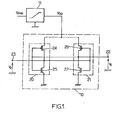
- the figure 1 represents a memory cell 10 of the SRAM type.
- This memory cell 10 is powered by a supply circuit 11.
- the supply circuit 11 is used to perform a progressive voltage rise of the supply voltage V DD of the cell.
- the memory cell 10 comprises two inverters 20 and 21 mounted head to tail, that is to say that each inverter has its output connected to the input of the other inverter.
- the output of the inverter 21 corresponds to an output terminal 22 of the memory cell 10, where a voltage V1 can be read.
- the output of the inverter 20 corresponds to an output terminal 23 of the memory cell 10 where a voltage V2 can be read.
- the inverter 20 comprises a PMOS transistor 24 and an NMOS transistor 25.
- the drains of the transistors 24 and 25 are connected together to form the output of the inverter 20.
- the gates of the transistors 24 and 25 are connected. together to form the input of the inverter 20 which is connected to the output of the inverter 21.
- the source of the transistor 25 is connected to the ground while the source of the transistor 24 receives the supply voltage V DD of the memory cell 10.
- the inverter 21 comprises a PMOS transistor 26 and an NMOS transistor 27. The drains of the transistors 26 and 27 are connected together and form the output of the inverter 21. The gates of transistors 26 and 27 are connected together and form the output of the inverter 21. The gates of transistors 26 and 27 are connected together and form the input of the inverter 21 which is connected to the output of the inverter 20. The source of the transistor 27 is connected to ground while the transistor source 26 receives the supply voltage of the memory cell 10.
- the output terminals of the inverters 22 and 23 are connected according to the type of application either directly to read amplifiers or to bit lines via link transistors, a bit line being common to a plurality of cells of memory.
- the bit lines are furthermore linked on the one hand to reading amplifiers, and on the other hand to writing amplifiers.
- the PMOS transistor when the input voltage of an inverter is at a low level, the PMOS transistor conducts and pulls the output to a high level. Conversely, when the input voltage is at a high level, the NMOS transistor drives and pulls the output voltage to a low level. In transient mode, the input voltage goes from a high level to a low level or goes from a low level to a high level. During this transition, the output of the inverter will switch when the voltage has reached a threshold voltage of the inverter.
- the threshold voltage of the inverter corresponds to an average of the intrinsic threshold voltages of the two transistors forming the inverter. Conventionally, the threshold voltages of each transistor are approximately the same in absolute value and the threshold voltage of the inverter corresponds to about half of the supply voltage.
- the supply voltage When establishing the supply voltage, the supply voltage itself has a transition.
- the input voltages of the inverters are determined by the ratio of the capacitances of the gates of the transistors of the inverters, which classically corresponds to about half of the supply voltage.
- this supply voltage exceeds twice the conduction threshold voltage of the NMOS transistor which is generally lower in absolute value than the threshold voltage of the PMOS transistor, the inverter starts to switch freely and its output is positioned at a low state.
- the input voltages of the two inverters correspond to half of the supply voltage until one of the inverters has not switched. And the positioning of the memory cell is done when the first of the two inverters starts to switch to print a low level on its output, which automatically causes the switchover of the other inverter to a high level.
- the determination of the inverter which topples first is very random, because it depends on minute differences related to manufacturing or parasitic phenomena.
- the principle implemented in the invention consists in having, in a given cell, two asymmetric inverters so that their threshold voltages are different. Asymmetry is obtained by performing an additional manufacturing step on only one of the transistors of the cell. Thus, one of the transistors will be depleted at its conduction channel.
- a supply circuit 11 provides a gentle slope on the growth of the supply voltage during power-up to ensure a slow tilting of the two cells. Indeed, if the voltage varies too abruptly, the phenomenon is more difficult to control. However, if it is a large memory, that is to say having a very large number of memory cells, the equivalent capacity corresponding to the matrix of cells may be sufficient to cause a smooth growth. of the supply voltage at power up and the circuit 11 is not necessary.
- the memory cell is for storing a unique code for each circuit
- the depletion step is still done but selectively.
- a photosensitive layer is produced which is selectively insolated with an electron beam (EBEAM) or with the aid of a laser.
- EBEAM electron beam
- the photosensitive layer is then developed and then proceeded to the implantation.
- Selective implantation is done during manufacture.
- the cells are programmed permanently and it is not possible to reprogram the cell.
- Depletion is achieved because the lowering of the threshold voltage makes it possible to react with a lower supply voltage than an enhanced threshold.
- the voltage V DD corresponds to the supply voltage of the memory cell 10. This supply voltage is initially at 0 volts and has a transition to arrive at a voltage V max corresponding to the supply voltage. This transition is represented with a steeper slope in order to better explain the operation.
- the voltage V1 represented on the figure 2 corresponds to the output voltage of the inverter 21 but also to the gate voltage / transistor source 25. On the timing diagram, there is shown a voltage level V T1 which corresponds to the threshold voltage of the NMOS transistor 25. This threshold voltage 21 is a little less than half the maximum voltage d supply V max .
- the voltage V1 - V DD shown corresponds to the gate / source voltage of the transistor 24 on which is represented the threshold voltage V T2 which is well below half the maximum supply voltage because this transistor is depleted. It should be noted that this voltage is negative because it is a PMOS transistor.
- the voltage V2 corresponds to the output voltage of the inverter 20 and the input voltage of the inverter 21. This voltage V2 also corresponds to the gate / source voltage of the transistor 27, the voltage V T3 corresponding to its voltage threshold.
- the voltage V1-V DD corresponds to the gate / source voltage of the transistor 26 on which is represented the threshold voltage V T4 corresponding to said transistor 26.
- the voltages V T1 , V T3 and V T4 in absolute values are practically equal. Strictly, the voltage V T4 is in absolute value slightly higher than the voltages V T1 and V T3 . On the other hand, the voltage V T2 is found to be much smaller, in absolute value, than all the other threshold voltages V T1 , V T3 and V T4 .
- this is a standard memory cell where the transistors are of the same size.
- the memory cell When powering up, the memory cell is in an undetermined state, all transistors being blocked.
- the input voltage of each of the inverters corresponds to a voltage defined by a voltage divider capacitive bridge which corresponds to the equivalent capacitances between gate and substrate of the transistors forming the cell. Since the transistors 24 to 27 have the same dimensions in terms of length and channel width, the capacitive bridge formed by each inverter makes it possible to have a gate voltage equal to half of the supply voltage as long as no transistor was made passing.
- the supply voltage V DD begins to grow in a gentle slope
- the V1 and V2 voltages grow but with a slope divided by two compared to the slope of the supply voltage V DD and, conversely, the voltages V1 - V DD and V2 - V DD decrease with a slope two times lower at the slope of the supply voltage V DD .
- the voltage V1 - V DD reaches the threshold voltage V T2 of the transistor 24. The transistor 24 then turns on and the voltage V2 begins to quickly reach the supply voltage V DD .
- the switching of the transistor 24 causes a faster slope than the growth slope of the supply voltage and, at a time t3, the voltage V2 reaches the threshold voltage V T3 of the transistor 27. This transistor 27 then begins to drive and returns the voltage V1 to the ground voltage (0 volts).
- the conduction of the transistor 24 returning the voltage V2 to the supply voltage also reduces the voltage V2 - V DD to a zero voltage.
- the transistor 26 remains always blocked.
- the conduction of the transistor 27 causes the voltage V1 to return to zero and thus keeps the transistor 25 blocked.
- This evolution of the voltage V1 brings the voltage V1 - V DD back to a voltage close to the voltage V DD which keeps the transistor 24 passing.
- the voltage V DD continues to settle until reaching a voltage V max and the cell is positioned in a predefined state by the depletion of the transistor 24.
- the level 0 or 1 of a cell is arbitrarily defined according to whether it is decided that the level 1 corresponds to a high voltage for V1 and a low voltage for V2 or vice versa.
- the programming of a cell will consist in the example described to deplete either transistor 24 or transistor 26 following the state 0 or 1 that it is desired to pre-register.
- the maximum supply voltage V max was at least twice greater than a threshold voltage in absolute value.
- the technology is evolving to use lower and higher supply voltages. This evolution of the technology means that the threshold voltages of the transistors tend to be greater in absolute value than half of the supply voltage. In such a case, high depletion is required to achieve the desired effect.
- it is possible to avoid excessive depletion it is possible to use a different dimensioning of the gate surfaces between the NMOS transistors and the PMOS transistors.
- an oversizing of the gate capacitances of the transistors opposite to the depleted transistor makes it possible to reach more rapidly the threshold voltage of the depleted transistor.
- the figure 3 corresponds to an embodiment where the threshold voltages V T1 , V T3 and V T4 are in absolute values, for example equal to two thirds of the maximum supply voltage V max .
- Transistor 24 is always a depleted transistor but with a threshold voltage reduced, for example, to about V max / 2.
- the NMOS transistors 25 and 27 have dimensions with respect to the PMOS transistors 24 and 26, in terms of the gate surface, such as the capacitive ratio created by the capacitance bridge.
- the voltages V1 and V2 evolve with a slope equal to one third of the slope of the voltage V DD until they are controlled by the conduction of one of the transistors 24 to 27.
- the gate voltages / source of the PMOS transistors 24 and 25 evolve with a slope equal to two-thirds of the slope of the voltage V DD .
- the voltage V1 - V DD may arrive at a time t2 at a voltage equal to the voltage V T2 , although it is equal to half the threshold voltage, and cause the same phenomenon of successive conductions of the transistor 24 then transistor 27.
- the transistors even if it is not possible to reach the threshold voltage of the transistors during power up, the positioning of the cell 10 in the desired level is achieved. For example, if the transistors have the same gate area with threshold voltages greater than half the maximum supply voltage V MAX , they will remain in a locked state after the voltage is set. power. However, even in the off state, the transistors pass a leakage current. The gates of an inverter are then charged or discharged by the difference of the leakage currents existing between the NMOS transistor and the PMOS transistor of the other inverter. In the case where the inverters are asymmetrical, the one which will have a threshold voltage far from V MAX / 2 will change the gate voltage of the other inverter which will then be unbalanced and amplify the tilt accordingly.
- An advantage of such a cell 10 is also to allow a circuit to have a stealth identification. Indeed, it is possible to access non-volatile information after power on and before writing it. So we can erase the non-volatile content after using it while keeping it hidden.
- the stealthiness can be increased in some cases by cutting off the power of the cells.
- Such a use allows a circuit to memorize a secret identification number and to be able to access it only if one feeds the cells to read it.
- the power supply of the cells can then be conditional, which reinforces the confidential nature of their content.
- control means can be provided for switching on or off the supply circuit which supplies the memory cells only for reading the contents of said cells.
- the memory cells may be dispersed among the logic circuits constituting the integrated circuit where they are placed.
Landscapes
- Engineering & Computer Science (AREA)
- Microelectronics & Electronic Packaging (AREA)
- Computer Hardware Design (AREA)
- Static Random-Access Memory (AREA)
- Semiconductor Memories (AREA)
Claims (7)
- Speicherzelle (10), umfassend zwei Inverter (20, 21), die entgegengesetzt angebracht sind, um ein Bit zu speichern, wobei jeder Inverter einen Transistor (24 oder 26) von einem ersten Typ und einen Transistor (25 oder 27) von einem zweiten Typ umfasst, wobei die Ladungsträger-Konzentration im Leitungskanal des Transistors (24) vom ersten Typ des einen der Inverter (20) verschieden von der Ladungsträger-Konzentration im Leitungskanal des Transistors (26) vom ersten Typ des anderen der Inverter (21) ist,
dadurch gekennzeichnet, dass der Transistor (24) vom ersten Typ von einem einzigen der Inverter ein Verarmungstransistor ist, so dass die Inverter unterschiedliche Schwellenspannungen haben, und dadurch, dass die Transistoren (25, 27) vom zweiten Typ eine in Bezug auf die Gate-Fläche der Transistoren (24, 26) vom ersten Typ verschiedene Gate-Fläche aufweisen, und dass die Gate-Kapazitäten der Transistoren vom zweiten Typ in Bezug auf die Gate-Kapazitäten der Transistoren vom ersten Typ überdimensioniert sind. - Speicherzelle nach Anspruch 1, wobei die Transistoren (24, 26) vom ersten Typ PMOS-Transistoren sind, und wobei die Transistoren (25, 27) vom zweiten Typ NMOS-Transistoren sind.
- Integrierter Schaltkreis, umfassend Zellen nach einem der Ansprüche 1 und 2 und einen Schaltkreis (11), der dazu geeignet ist, den Zellen beim Anlegen von Spannung eine Versorgungsspannung mit einem sanften Gefälle zu liefern.
- Integrierter Schaltkreis nach Anspruch 3, umfassend weiter Steuer-/Regel-Mittel, um an den Versorgungs-Schaltkreis, der die Zellen versorgt, eine Spannung anzulegen oder ihn von der Spannung zu trennen, wobei der Steuer-/Regel-Schaltkreis dazu geeignet ist, an den Versorgungs-Schaltkreis eine Spannung anzulegen, nur um den Inhalt der Zellen auszulesen.
- Integrierter Schaltkreis nach einem der Ansprüche 3 und 4, wobei die Zellen unter den Logik-Schaltkreisen, die den integrierten Schaltkreis bilden, verteilt sind.
- Elektronischer Speicher-Schaltkreis, verwirklicht auf einem Halbleiter-Chip, wobei der Schaltkreis eine Mehrzahl von elementaren Zellen zur Speicherung umfasst, wobei jede elementare Zelle ein Bit mittels zwei entgegengesetzt angebrachten Inverter speichern kann, dadurch gekennzeichnet, dass er weiter wenigstens eine Zelle (10) nach Anspruch 1 umfasst.
- Speicher-Schaltkreis nach Anspruch 6, wobei die Transistoren vom ersten Typ PMOS-Transistoren sind und wobei die Transistoren vom zweiten Typ NMOS-Transistoren sind.
Applications Claiming Priority (1)
| Application Number | Priority Date | Filing Date | Title |
|---|---|---|---|
| FR0411360A FR2877143A1 (fr) | 2004-10-25 | 2004-10-25 | Cellule de memoire volatile preenregistree |
Publications (2)
| Publication Number | Publication Date |
|---|---|
| EP1650806A1 EP1650806A1 (de) | 2006-04-26 |
| EP1650806B1 true EP1650806B1 (de) | 2010-05-12 |
Family
ID=34952238
Family Applications (1)
| Application Number | Title | Priority Date | Filing Date |
|---|---|---|---|
| EP05292134A Not-in-force EP1650806B1 (de) | 2004-10-25 | 2005-10-12 | Vorbespielte flüchtige Speicherzelle |
Country Status (4)
| Country | Link |
|---|---|
| US (1) | US7289355B2 (de) |
| EP (1) | EP1650806B1 (de) |
| DE (1) | DE602005021192D1 (de) |
| FR (1) | FR2877143A1 (de) |
Families Citing this family (3)
| Publication number | Priority date | Publication date | Assignee | Title |
|---|---|---|---|---|
| PL1670433T3 (pl) * | 2003-10-10 | 2013-03-29 | Ferring Bv | Przezskórna formulacja farmaceutyczna do zmniejszania pozostałości na skórze |
| US8690065B2 (en) | 2007-08-15 | 2014-04-08 | Nxp B.V. | Secure storage of a codeword within an integrated circuit |
| TW201023341A (en) * | 2008-12-12 | 2010-06-16 | Ind Tech Res Inst | Integrated circuit structure |
Family Cites Families (8)
| Publication number | Priority date | Publication date | Assignee | Title |
|---|---|---|---|---|
| US4821233A (en) * | 1985-09-19 | 1989-04-11 | Xilinx, Incorporated | 5-transistor memory cell with known state on power-up |
| JPS6381974A (ja) * | 1986-09-26 | 1988-04-12 | Hitachi Ltd | 半導体集積回路装置の製造方法 |
| JP2550207B2 (ja) * | 1990-06-08 | 1996-11-06 | 株式会社東芝 | 半導体メモリセル |
| US5239510A (en) * | 1991-11-25 | 1993-08-24 | At&T Bell Laboratories | Multiple voltage supplies for field programmable gate arrays and the like |
| JP3637299B2 (ja) * | 2001-10-05 | 2005-04-13 | 松下電器産業株式会社 | 半導体記憶装置 |
| US20030218218A1 (en) * | 2002-05-21 | 2003-11-27 | Samir Chaudhry | SRAM cell with reduced standby leakage current and method for forming the same |
| JP4162076B2 (ja) * | 2002-05-30 | 2008-10-08 | 株式会社ルネサステクノロジ | 半導体記憶装置 |
| FR2849260B1 (fr) | 2002-12-23 | 2005-03-11 | St Microelectronics Sa | Cellule de memoire sram non volatile. |
-
2004
- 2004-10-25 FR FR0411360A patent/FR2877143A1/fr active Pending
-
2005
- 2005-10-12 DE DE602005021192T patent/DE602005021192D1/de active Active
- 2005-10-12 EP EP05292134A patent/EP1650806B1/de not_active Not-in-force
- 2005-10-25 US US11/261,396 patent/US7289355B2/en active Active
Also Published As
| Publication number | Publication date |
|---|---|
| US20060139990A1 (en) | 2006-06-29 |
| EP1650806A1 (de) | 2006-04-26 |
| FR2877143A1 (fr) | 2006-04-28 |
| US7289355B2 (en) | 2007-10-30 |
| DE602005021192D1 (de) | 2010-06-24 |
Similar Documents
| Publication | Publication Date | Title |
|---|---|---|
| EP0080394B1 (de) | Bistabile Kippschaltung mit energieunabhängiger Haltbarkeit und statischer Rücksetzung | |
| EP1833090B1 (de) | Speicherzellen der CMOS-Technologie mit Doppel-Gate, die mit Transistoren mit zwei unabhängigen Gates ausgestattet sind | |
| EP1434237B1 (de) | Nichtflüchtige SRAM Speicherzelle | |
| FR2787922A1 (fr) | Cellule memoire a programmation unique en technologie cmos | |
| FR2610135A1 (fr) | Memoire a semiconducteurs a lignes de donnees differentielles | |
| EP3010022B1 (de) | Speicherzelle mit lese-transistoren vom typ tfet und mosfet | |
| FR2957449A1 (fr) | Micro-amplificateur de lecture pour memoire | |
| EP0080395B1 (de) | Bistabile Kippschaltung mit energieunabhängiger Haltbarkeit und dynamischer Rücksetzung | |
| EP1650806B1 (de) | Vorbespielte flüchtige Speicherzelle | |
| EP0121464B1 (de) | Nichtflüchtige RAM Speicherzelle mit CMOS Transistoren mit gemeinsamem schwebendem Gate | |
| FR2871282A1 (fr) | Dispositif memoire programmable une seule fois | |
| EP2286450B1 (de) | Schreibgeschützter speicher mit eeprom-struktur | |
| FR2751778A1 (fr) | Memoire accessible en lecture seulement | |
| FR2921508A1 (fr) | Memoire sram a cellule de reference de polarisation | |
| EP2003650B1 (de) | Asymmetrische SRAM-Speicherzelle mit 4 Doppelgate-Transistoren | |
| EP0915480B1 (de) | Nichtflüchtiger MOS-Speicher | |
| FR2955195A1 (fr) | Dispositif de comparaison de donnees dans une memoire adressable par contenu sur seoi | |
| FR2844090A1 (fr) | Cellule memoire pour registre non volatile a lecture rapide | |
| EP1818942A1 (de) | Nichtflüchtige Speichervorrichtung | |
| FR2878068A1 (fr) | Memoire a cellule de memorisation polarisee par groupe | |
| EP2977988B1 (de) | Nicht-flüchtiger speicher mit programmierbarem widerstand | |
| FR2929751A1 (fr) | Procede de programmation d'un dispositif de memoire du type programmable une fois et circuit integre incorporant un tel dispositif de memoire | |
| EP1624460B1 (de) | Speicher mit einem Speicherpunkt vom SRAM-Typ, dazugehörige Lese-und Schreibverfahren | |
| EP1158408A1 (de) | EEPROM Speicher mit Fehlerkorrekturvorrichtung | |
| EP0996064B1 (de) | Einmalig programmierbare Speicherzelle |
Legal Events
| Date | Code | Title | Description |
|---|---|---|---|
| PUAI | Public reference made under article 153(3) epc to a published international application that has entered the european phase |
Free format text: ORIGINAL CODE: 0009012 |
|
| AK | Designated contracting states |
Kind code of ref document: A1 Designated state(s): AT BE BG CH CY CZ DE DK EE ES FI FR GB GR HU IE IS IT LI LT LU LV MC NL PL PT RO SE SI SK TR |
|
| AX | Request for extension of the european patent |
Extension state: AL BA HR MK YU |
|
| 17P | Request for examination filed |
Effective date: 20061017 |
|
| AKX | Designation fees paid |
Designated state(s): DE FR GB IT |
|
| 17Q | First examination report despatched |
Effective date: 20061227 |
|
| GRAP | Despatch of communication of intention to grant a patent |
Free format text: ORIGINAL CODE: EPIDOSNIGR1 |
|
| GRAS | Grant fee paid |
Free format text: ORIGINAL CODE: EPIDOSNIGR3 |
|
| GRAA | (expected) grant |
Free format text: ORIGINAL CODE: 0009210 |
|
| AK | Designated contracting states |
Kind code of ref document: B1 Designated state(s): DE FR GB IT |
|
| REG | Reference to a national code |
Ref country code: GB Ref legal event code: FG4D Free format text: NOT ENGLISH |
|
| REF | Corresponds to: |
Ref document number: 602005021192 Country of ref document: DE Date of ref document: 20100624 Kind code of ref document: P |
|
| PGFP | Annual fee paid to national office [announced via postgrant information from national office to epo] |
Ref country code: IT Payment date: 20100925 Year of fee payment: 6 |
|
| PGFP | Annual fee paid to national office [announced via postgrant information from national office to epo] |
Ref country code: GB Payment date: 20100928 Year of fee payment: 6 |
|
| PGFP | Annual fee paid to national office [announced via postgrant information from national office to epo] |
Ref country code: DE Payment date: 20100930 Year of fee payment: 6 |
|
| PLBE | No opposition filed within time limit |
Free format text: ORIGINAL CODE: 0009261 |
|
| STAA | Information on the status of an ep patent application or granted ep patent |
Free format text: STATUS: NO OPPOSITION FILED WITHIN TIME LIMIT |
|
| 26N | No opposition filed |
Effective date: 20110215 |
|
| REG | Reference to a national code |
Ref country code: DE Ref legal event code: R097 Ref document number: 602005021192 Country of ref document: DE Effective date: 20110214 |
|
| PGFP | Annual fee paid to national office [announced via postgrant information from national office to epo] |
Ref country code: FR Payment date: 20111205 Year of fee payment: 7 |
|
| GBPC | Gb: european patent ceased through non-payment of renewal fee |
Effective date: 20111012 |
|
| PG25 | Lapsed in a contracting state [announced via postgrant information from national office to epo] |
Ref country code: DE Free format text: LAPSE BECAUSE OF NON-PAYMENT OF DUE FEES Effective date: 20120501 |
|
| REG | Reference to a national code |
Ref country code: DE Ref legal event code: R119 Ref document number: 602005021192 Country of ref document: DE Effective date: 20120501 |
|
| PG25 | Lapsed in a contracting state [announced via postgrant information from national office to epo] |
Ref country code: GB Free format text: LAPSE BECAUSE OF NON-PAYMENT OF DUE FEES Effective date: 20111012 Ref country code: IT Free format text: LAPSE BECAUSE OF NON-PAYMENT OF DUE FEES Effective date: 20111012 |
|
| REG | Reference to a national code |
Ref country code: FR Ref legal event code: ST Effective date: 20130628 |
|
| PG25 | Lapsed in a contracting state [announced via postgrant information from national office to epo] |
Ref country code: FR Free format text: LAPSE BECAUSE OF NON-PAYMENT OF DUE FEES Effective date: 20121031 |