EP1648060B1 - Oberflächenemittierender Laser mit externem vertikalem Resonator (VECSEL) und mit stromführender Struktur - Google Patents
Oberflächenemittierender Laser mit externem vertikalem Resonator (VECSEL) und mit stromführender Struktur Download PDFInfo
- Publication number
- EP1648060B1 EP1648060B1 EP20050256393 EP05256393A EP1648060B1 EP 1648060 B1 EP1648060 B1 EP 1648060B1 EP 20050256393 EP20050256393 EP 20050256393 EP 05256393 A EP05256393 A EP 05256393A EP 1648060 B1 EP1648060 B1 EP 1648060B1
- Authority
- EP
- European Patent Office
- Prior art keywords
- layer
- gaas
- reflective layer
- substrate
- semiconductor layer
- Prior art date
- Legal status (The legal status is an assumption and is not a legal conclusion. Google has not performed a legal analysis and makes no representation as to the accuracy of the status listed.)
- Expired - Lifetime
Links
Images


Classifications
-
- H—ELECTRICITY
- H01—ELECTRIC ELEMENTS
- H01S—DEVICES USING THE PROCESS OF LIGHT AMPLIFICATION BY STIMULATED EMISSION OF RADIATION [LASER] TO AMPLIFY OR GENERATE LIGHT; DEVICES USING STIMULATED EMISSION OF ELECTROMAGNETIC RADIATION IN WAVE RANGES OTHER THAN OPTICAL
- H01S5/00—Semiconductor lasers
- H01S5/10—Construction or shape of the optical resonator, e.g. extended or external cavity, coupled cavities, bent-guide, varying width, thickness or composition of the active region
- H01S5/18—Surface-emitting [SE] lasers, e.g. having both horizontal and vertical cavities
- H01S5/183—Surface-emitting [SE] lasers, e.g. having both horizontal and vertical cavities having only vertical cavities, e.g. vertical cavity surface-emitting lasers [VCSEL]
- H01S5/18308—Surface-emitting [SE] lasers, e.g. having both horizontal and vertical cavities having only vertical cavities, e.g. vertical cavity surface-emitting lasers [VCSEL] having a special structure for lateral current or light confinement
- H01S5/18322—Position of the structure
- H01S5/1833—Position of the structure with more than one structure
- H01S5/18333—Position of the structure with more than one structure only above the active layer
-
- H—ELECTRICITY
- H01—ELECTRIC ELEMENTS
- H01S—DEVICES USING THE PROCESS OF LIGHT AMPLIFICATION BY STIMULATED EMISSION OF RADIATION [LASER] TO AMPLIFY OR GENERATE LIGHT; DEVICES USING STIMULATED EMISSION OF ELECTROMAGNETIC RADIATION IN WAVE RANGES OTHER THAN OPTICAL
- H01S3/00—Lasers, i.e. devices using stimulated emission of electromagnetic radiation in the infrared, visible or ultraviolet wave range
- H01S3/10—Controlling the intensity, frequency, phase, polarisation or direction of the emitted radiation, e.g. switching, gating, modulating or demodulating
- H01S3/106—Controlling the intensity, frequency, phase, polarisation or direction of the emitted radiation, e.g. switching, gating, modulating or demodulating by controlling devices placed within the cavity
- H01S3/108—Controlling the intensity, frequency, phase, polarisation or direction of the emitted radiation, e.g. switching, gating, modulating or demodulating by controlling devices placed within the cavity using non-linear optical devices, e.g. exhibiting Brillouin or Raman scattering
- H01S3/109—Frequency multiplication, e.g. harmonic generation
-
- H—ELECTRICITY
- H01—ELECTRIC ELEMENTS
- H01S—DEVICES USING THE PROCESS OF LIGHT AMPLIFICATION BY STIMULATED EMISSION OF RADIATION [LASER] TO AMPLIFY OR GENERATE LIGHT; DEVICES USING STIMULATED EMISSION OF ELECTROMAGNETIC RADIATION IN WAVE RANGES OTHER THAN OPTICAL
- H01S5/00—Semiconductor lasers
- H01S5/10—Construction or shape of the optical resonator, e.g. extended or external cavity, coupled cavities, bent-guide, varying width, thickness or composition of the active region
- H01S5/14—External cavity lasers
- H01S5/141—External cavity lasers using a wavelength selective device, e.g. a grating or etalon
-
- H—ELECTRICITY
- H01—ELECTRIC ELEMENTS
- H01S—DEVICES USING THE PROCESS OF LIGHT AMPLIFICATION BY STIMULATED EMISSION OF RADIATION [LASER] TO AMPLIFY OR GENERATE LIGHT; DEVICES USING STIMULATED EMISSION OF ELECTROMAGNETIC RADIATION IN WAVE RANGES OTHER THAN OPTICAL
- H01S5/00—Semiconductor lasers
- H01S5/10—Construction or shape of the optical resonator, e.g. extended or external cavity, coupled cavities, bent-guide, varying width, thickness or composition of the active region
- H01S5/18—Surface-emitting [SE] lasers, e.g. having both horizontal and vertical cavities
- H01S5/183—Surface-emitting [SE] lasers, e.g. having both horizontal and vertical cavities having only vertical cavities, e.g. vertical cavity surface-emitting lasers [VCSEL]
- H01S5/18308—Surface-emitting [SE] lasers, e.g. having both horizontal and vertical cavities having only vertical cavities, e.g. vertical cavity surface-emitting lasers [VCSEL] having a special structure for lateral current or light confinement
- H01S5/18311—Surface-emitting [SE] lasers, e.g. having both horizontal and vertical cavities having only vertical cavities, e.g. vertical cavity surface-emitting lasers [VCSEL] having a special structure for lateral current or light confinement using selective oxidation
-
- H—ELECTRICITY
- H01—ELECTRIC ELEMENTS
- H01S—DEVICES USING THE PROCESS OF LIGHT AMPLIFICATION BY STIMULATED EMISSION OF RADIATION [LASER] TO AMPLIFY OR GENERATE LIGHT; DEVICES USING STIMULATED EMISSION OF ELECTROMAGNETIC RADIATION IN WAVE RANGES OTHER THAN OPTICAL
- H01S5/00—Semiconductor lasers
- H01S5/20—Structure or shape of the semiconductor body to guide the optical wave ; Confining structures perpendicular to the optical axis, e.g. index or gain guiding, stripe geometry, broad area lasers, gain tailoring, transverse or lateral reflectors, special cladding structures, MQW barrier reflection layers
- H01S5/2054—Methods of obtaining the confinement
- H01S5/2059—Methods of obtaining the confinement by means of particular conductivity zones, e.g. obtained by particle bombardment or diffusion
- H01S5/2063—Methods of obtaining the confinement by means of particular conductivity zones, e.g. obtained by particle bombardment or diffusion obtained by particle bombardment
-
- H—ELECTRICITY
- H01—ELECTRIC ELEMENTS
- H01S—DEVICES USING THE PROCESS OF LIGHT AMPLIFICATION BY STIMULATED EMISSION OF RADIATION [LASER] TO AMPLIFY OR GENERATE LIGHT; DEVICES USING STIMULATED EMISSION OF ELECTROMAGNETIC RADIATION IN WAVE RANGES OTHER THAN OPTICAL
- H01S5/00—Semiconductor lasers
- H01S5/30—Structure or shape of the active region; Materials used for the active region
- H01S5/305—Structure or shape of the active region; Materials used for the active region characterised by the doping materials used in the laser structure
- H01S5/3054—Structure or shape of the active region; Materials used for the active region characterised by the doping materials used in the laser structure p-doping
-
- H—ELECTRICITY
- H01—ELECTRIC ELEMENTS
- H01S—DEVICES USING THE PROCESS OF LIGHT AMPLIFICATION BY STIMULATED EMISSION OF RADIATION [LASER] TO AMPLIFY OR GENERATE LIGHT; DEVICES USING STIMULATED EMISSION OF ELECTROMAGNETIC RADIATION IN WAVE RANGES OTHER THAN OPTICAL
- H01S5/00—Semiconductor lasers
- H01S5/30—Structure or shape of the active region; Materials used for the active region
- H01S5/305—Structure or shape of the active region; Materials used for the active region characterised by the doping materials used in the laser structure
- H01S5/3095—Tunnel junction
Definitions
- the present invention is related to a semiconductor laser, and more particularly to surface emitting lasers and vertical external cavity surface emitting lasers (VECSEL).
- VECSEL vertical external cavity surface emitting lasers
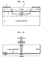
- a conventional vertical cavity surface emitting laser is illustrated in a cross-sectional view.
- the various layers of the VCSEL include an n-GaAs (Gallium Arsenide) substrate 2, an active layer 6 between an n-DBR (distributed Bragg reflector) layer 4 and a p-DBR (distributed Bragg reflector) layer 8, and a top conductive layer 10.
- the (optical) cavity 12 is perpendicular to the layers, which allows for the optical beam to be emitted in the vertical direction. In the configuration illustrated the aperture is approximately 20 ⁇ m.
- the conventional VCSEL design is limited in its fundamental transverse operation mode. For example, it is difficult to achieve designs that generate a single mode signal with greater than 7-8 ⁇ m apertures, which limits the fundamental transverse power mode in the conventional VCSEL.
- Fig. 1B illustrates a related art Novalux Extended Cavity Surface Emitting Laser (NECSEL) as discloses in U.S. Patent No. 6,243,407 .
- the NECSEL laser's emitting area is said to be tens of times larger than conventional VCSELs, thereby allowing scaling to high power levels.
- the larger emitting area was designed to address the current crowding problems with the conventional VCSEL designs.
- the substrate thick it is said to provide enough distance from the active region such that the carriers can diffuse laterally and thereby provide a more uniform carrier distribution in the active region.
- the NECSEL uses an extremely thick GaAs substrate 20 (e.g. >100um)
- US 5,493,577 describes a number of VCSEL structures.
- an aperture is provided above an active region, an upper mirror above the aperture, and an electrode with an opening above the lower aperture.
- the current path is narrower through the aperture.
- a surface emitting laser apparatus includes a first substrate disposed between a first electrode layer and a first reflective layer.
- An active region is disposed between the first reflective layer and a second reflective layer.
- a current blocking layer is disposed between the active region and a second electrode layer to form an aperture.
- a first semiconductor layer can be disposed between the second electrode layer and the second reflective layer.
- the second electrode layer can have an opening substantially aligned with the aperture.
- a current funnel region can be located in a cavity formed between the aperture and the opening of the second electrode. The current funnel region can be configured to facilitate conduction through the cavity.
- Fig. 2A illustrates at least one exemplary embodiment of the invention.
- an undoped or n-doped Gallium Arsenide (n-GaAs) layer 210 and a p-GaAs layer 212 can be grown on p-DBR layer 208.
- the reflectivity of the p-DBR layer can vary (e.g., in a range from about 30% to 90%).
- the carriers are prevented from passing through the undoped or n-doped GaAs because of the p-n-p structure, but without substantially attenuating the light generated in the active region 206.
- a funnel like current pass region 220 can be formed toward the center of the vertical cavity.
- Zn zinc
- a funnel like current pass region 220 can be formed toward the center of the vertical cavity.
- more than one region can be formed in the vertical cavity and multiple regions of uniform or varying dimensions can be used to further adjust or optimize the carrier profile.
- the base substructure is similar to the conventional VCSEL construction. Accordingly, a detailed explanation of the layers and operation will not be provided.
- the p-n-p structure described above is located on the conventional VCSEL construction. Specifically, the n-GaAs substrate 202, n-DBR layer 204, active region 206, insulator (e.g., oxide) layer 207 and p-DBR layer 208 form the base structure.
- the un-doped or n-doped (n-GaAs) layer 210 and a p-GaAs layer 212 are located above the p-DBR layer 208, which forms the p-n-p structure that generally prevents carrier conduction between the layers.
- the current funnel region 220 formed across the p-n-p structure facilitates carrier conduction (e.g., as illustrated by arrows 218) in the cavity. As illustrated, the current funnel region 220 is generally aligned with the cavity formed by the top electrode 214 and aperture 216.
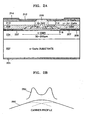
- the carrier profile of the embodiment of Fig. 2A is illustrated.
- the carrier profile is determined by two-step diffusion through the current funnel region and the active region.
- the carrier profile through the current funnel region (e.g., Zn diffusion) 250 and active region 260 is illustrated.
- a uniform carrier distribution 260 can be obtained at the active region when compared to the conventional carrier profile 14 of Fig. 1A .
- the uniform active region size can be controlled by, the thickness of top GaAs layer, undoped or n-doped GaAs layer, p-DBR layer and the size of the funnel. For example, a narrower width of the funnel promotes a uniform carrier profile at the active region.
- the thickness of the p-DBR layer is increased.
- the p-DBR layer thickness can be increased by various techniques, such as using 3/4 lambda layers instead of 1/4 lambda layers and /or inserting a p-GaAs dummy layer on the top of the DBR.
- the embodiment of Fig. 2A can be generally considered to be a hole carrier configuration.
- the Zn is used as an acceptor dopant to form the current funnel region; however, other types of acceptor dopants can be used as will be appreciated by those skilled in the art.
- the embodiment illustrated in Fig. 3 is an electron carrier configuration and has a n-p-n structure and uses a donor type dopant (e.g., Si). Further, those skilled in the art will appreciate that the voltage bias will be reversed from the hole carrier configuration (e.g., the top electrode is the ground electrode).
- the base structure is formed by a p-GaAs substrate 302, p-DBR layer 304, active region 306, insulator (e.g., oxide) layer 307 and n-DBR layer 408.
- a p-GaAs layer 310 and n-GaAs layer 312 are located above the n-DBR layer 308, which forms the n-p-n structure that generally prevents carrier conduction between the layers.
- the current funnel region 320 formed across the n-p-n structure in the cavity is a silicon (Si) diffusion region. As illustrated, the current funnel region 320 is generally aligned with the cavity formed by the top electrode 314 and aperture 316. Generally, the electron carrier configuration of Fig. 3 has a flatter carrier profile in the active region than the hole carrier configuration of Fig. 2A .
- FIG. 4 another alternative embodiment of the invention is illustrated.
- This configuration can be also referred to as an electron carrier configuration and generally has a donor dopant type.
- the base structure includes a tunnel junction 425 and has similar type reflective layers 404 and 408.
- the base structure is formed by a n-GaAs substrate 402, a first n-DBR layer 304, active region 406, insulator (e.g., oxide) layer 407 and a second n-DBR layer 408.
- a tunnel junction is located between the active region 406 and the second n-DBR layer 408.
- the tunnel junction 425 is formed of a highly doped n + /p + junction as is known in the art.
- a p-GaAs layer 410 and n-GaAs layer 412 are located above the n-DBR layer 408, which forms the n-p-n structure that generally prevents carrier conduction between the layers.
- the current funnel region 420 formed across the n-p-n structure in the cavity is a silicon (Si) diffusion region. As illustrated, the current funnel region 420 is generally aligned with the cavity formed by the top electrode 414 and aperture 416. Incorporating the tunnel junction 425 allows the for the n-p-n structure to be used with the n-GaAs base substrate configuration. As discussed above, because electron diffusion (as opposed to hole diffusion) is used this configuration has a flatter carrier profile in the active region 406 and faster carrier mobility than the configuration of Fig. 2A .
- an embodiment of the invention can include a surface emitting laser apparatus comprising a first substrate (e.g., 202, 302, 402) disposed between a first electrode layer (e.g., 201, 301, 401) and a first reflective layer (e.g., 204, 304, 404).
- An active region e.g., 206, 306, 406 can be disposed between the first reflective layer and a second reflective layer (e.g., 208, 308, 408).
- a current blocking layer (e.g., 207, 307, 407) can be disposed above the active region to form an aperture (e.g., 216, 316, 416).
- a first semiconductor layer e.g., 210, 310, 410
- a second semiconductor layer e.g., 212, 312, 412
- the second electrode layer can have an opening substantially aligned with the aperture.
- a current funnel region (e.g., 220, 320, 420) can be located in a cavity formed between the aperture and the opening of the second electrode. The current funnel region can be configured to facilitate conduction across the second semiconductor layer, the first semiconductor layer, and second reflective layer.
- the first substrate and the first reflective layer can be of the same doping (e.g., n-type or p-type).
- the second reflective layer is of an opposite doping.
- the first semiconductor layer is of opposite doping from the second semiconductor layer.
- the first substrate is an n-GaAs substrate
- the first reflective layer is an n-DBR layer
- the second reflective layer is a p-DBR layer
- the first and second semiconductor layers are n-GaAs and p-GaAs, respectively.
- Fig. 2A the first substrate is an n-GaAs substrate
- the first reflective layer is an n-DBR layer
- the second reflective layer is a p-DBR layer
- the first and second semiconductor layers are n-GaAs and p-GaAs, respectively.
- first substrate is a p-GaAs substrate
- the first reflective layer is a p-DBR layer
- the second reflective layer is a n-DBR layer
- the first and second semiconductor layers are p-GaAs and n-GaAs, respectively.
- a tunnel junction layer can be disposed between the active region and the second reflective layer.
- the first substrate and the first and second reflective layers are of the same doping.
- the first semiconductor layer is still of opposite doping from the second semiconductor layer.
- the first substrate can be an n-GaAs substrate
- the first reflective and second reflective layers are n-DBR
- the first and second semiconductor layers are p-GaAs and n-GaAs, respectively.
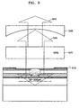
- a surface emitting laser apparatus 510 such as those discussed above can further include an output coupler 530 and a non-linear optical element 520.
- the non-linear optical element 520 is disposed between the second conductor 515 and the output coupler 530.
- the non-linear optical element 520 and output coupler 530 are substantially aligned with the cavity formed between the aperture and the opening of the second electrode 515.
- the non-linear optical element 520 can be a frequency doubling element such as a second-harmonic-generation (SHG) crystal to double an output frequency the surface emitting laser.
- SHG second-harmonic-generation
- the infrared laser beam 525 is converted to visible light laser beam 535 and propagated from the output coupler 530.
- non-linear optical element 520 and output coupler 530 are located external to the surface emitting laser apparatus 510, thus forming a VECSEL.
- the DBR layers can be formed of 4 ⁇ 40 pairs of AlAs / GaAs or AI(Ga)As/(AI)GaAs to provide high reflectivity for the laser cavity and prevent carrier diffusion.
- the active region can include 1 ⁇ 3 quantum wells (QW) as pump absorption and gain regions.
- QW quantum wells
- InGaAs QWs or InGaAs Quantum dot, or InAs(N) QD, or GaInNAs QW or QD
- GaAsP layers can provide strain relief.
- zinc (Zn) other acceptors such as Mg or C can be used to form the current funnel region.
- the current blocking layer 607 can be disposed on the second reflective layer 608.
- alternate embodiments of the invention can include the alternate location of the current blocking layer as illustrated in Fig. 6 .
- the active region 606 can be disposed between the first reflective layer 604 and the second reflective layer 608.
- a current blocking layer 607 can be disposed on the second reflective layer 608 to form an aperture.
- a first semiconductor layer 610 and a second semiconductor layer 612 can be disposed between a second electrode layer 614 and the second reflective layer 608.
- the second electrode layer 614 can have an opening substantially aligned with the aperture.
- a current funnel region 620 can be located in a cavity formed between the aperture and the opening of the second electrode.
- the current funnel region can be configured to facilitate conduction across the second semiconductor layer, the first semiconductor layer, and second reflective layer, as in the previously illustrated embodiments. All layers have not been illustrated in Fig. 6 to emphasize that the embodiments of Figs. 2A , 3 and 4 can be modified to correspond to the configuration illustrated in Fig. 6 . Accordingly, these and other modifications to the illustrated embodiments are considered to be within the scope of the present invention and the present invention is not limited to the arrangements illustrated herein.
- embodiments of the present invention achieve low free carrier absorption, without resorting to the thick n-GaAs substrate of the NECSEL design.
- embodiments of the invention allow for simple processing (i.e., no back side processing is required). Further, efficient frequency doubling can be achieved and a compact array is possible due to smaller size, when compared to the NECSEL design.
- conventional techniques can be used in forming the present invention.
- Fig. 7 Another example is illustrated in Fig. 7 , but not necessarily according to the present invention.
- an ion or proton implantation technique can be used to define a funnel structure as illustrated in Fig. 7 .
- the n-p-n or p-n-p current blocking structures previously discussed is not used in this embodiment.
- an electrode layer 701, an n-GaAs substrate 702, n-DBR layer 704, active region 706, insulator (e.g., oxide) layer 707 and p-DBR layer 708 form the base structure.
- a p-GaAs layer 710 is located between the p-DBR layer 708 and a second electrode layer 714.
- the current funnel region 720 is defined by a high resistivity region 712 (e.g., formed by proton implantation in p-GaAs layer 710) that is generally aligned with the cavity formed by the top electrode 714 and aperture 716.
- an example can include a surface emitting laser apparatus having a first substrate (e.g., 702) disposed between a first electrode layer (e.g., 701) and a first reflective layer (e.g., 704).
- An active region e.g., 706) can be disposed between the first reflective layer and a second reflective layer (e.g., 708).
- a current blocking layer e.g., 707 can be disposed between the active region and a second electrode layer (e.g., 708) to form an aperture.
- a first semiconductor layer e.g., 710 can be disposed between the second electrode layer and the second reflective layer.
- the second electrode layer has an opening substantially aligned with the aperture.
- a current funnel region (e.g., 720) can be located in a cavity between the aperture and the opening of the second electrode and is configured to facilitate conduction in the cavity. Additionally, the current funnel region can be defined by a high resistivity region (e.g., 712) disposed about the cavity in the first semiconductor layer. The high resistivity region can be formed by at least one of proton implantation and ion implantation.
- the first substrate can be an n-GaAs substrate, the first reflective layer an n-DBR layer, the second reflective layer a p-DBR layer, and the first semiconductor layer a p-GaAs layer.
- the first substrate can be a p-GaAs substrate, the first reflective layer a p-DBR layer, the second reflective layer an n-DBR layer, and the first semiconductor layer an n-GaAs layer.
- the active region can be formed of multiple quantum wells, as previously discussed.
- an output coupler and a non-linear optical element can be disposed between the second electrode and the output coupler,
- the non-linear optical element and the output coupler are substantially aligned with the cavity formed between the aperture and the opening of the second electrode external to the second electrode layer to form a vertical external cavity surface emitting laser (VECSEL), such as illustrated in Fig. 5 .
- VECSEL vertical external cavity surface emitting laser
Landscapes
- Physics & Mathematics (AREA)
- Condensed Matter Physics & Semiconductors (AREA)
- General Physics & Mathematics (AREA)
- Electromagnetism (AREA)
- Optics & Photonics (AREA)
- Semiconductor Lasers (AREA)
- Optical Modulation, Optical Deflection, Nonlinear Optics, Optical Demodulation, Optical Logic Elements (AREA)
Claims (24)
- Oberflächenemittierende Laservorrichtung umfassend:ein erstes Substrat (202, 302, 402, 702), das zwischen einer ersten Elektrodenschicht (201) und einer ersten Reflexionsschicht (204, 304, 404, 604, 704) angeordnet ist,eine zweite Elektrodenschicht (214, 314, 414, 614, 714) mit einer Öffnung,eine aktive Region (206, 306, 406, 606, 706), die zwischen der ersten Reflexionsschicht und einer zweiten Reflexionsschicht (208, 308, 408, 608, 708) angeordnet ist,eine Stromsperrschicht (207, 307, 407, 607, 707), die zwischen der aktiven Region (206, 306, 406, 606, 706) und der zweiten Elektrodenschicht (214, 314, 414, 614, 714) so angeordnet ist, dass sie eine Apertur (216, 316, 416, 616, 716) bildet, die mit der Öffnung fluchtet, undeine erste Halbleiterschicht (210, 310, 410, 610, 710), die zwischen der zweiten Elektrodenschicht (214, 314, 414, 614, 714) und der zweiten Reflexionsschicht (208, 308, 408, 608, 708) angeordnet ist,gekennzeichnet durch eine Stromführungsregion, die eine dotierte Region mit erhöhter Leitfähigkeit aufweist, die sich durch die erste Halbleiterschicht (210, 310, 410, 610, 710) erstreckt, wobei die Stromführungsregion eine Region mit höherer Leitfähigkeit als die sie seitlich umgebende Region ist, so dass Strom geführt wird.
- Vorrichtung nach Anspruch 1, wobei die Stromführungsregion in einer Kavität liegt und so konfiguriert ist, dass sie Leitung in der Kavität erleichtert.
- Vorrichtung nach Anspruch 1, ferner umfassend:eine zweite Halbleiterschicht (212, 312, 412, 612, 712), die zwischen der ersten Halbleiterschicht (210, 310, 410, 610, 710) und der zweiten Elektrode (214, 314, 414, 614, 714) angeordnet ist, wobei die zweite Reflexionsschicht (208, 308, 408, 608, 708), die erste Halbleiterschicht (210, 310, 410, 610, 710) und die zweite Halbleiterschicht (212, 312, 412, 612, 712) eine p-n-p-Struktur bilden und wobei die Stromführungsregion durch Zink(Zn)-Diffusion und/oder Zink(Zn)-Implantation in der Kavität gebildet ist.
- Vorrichtung nach Anspruch 3, wobei das erste Substrat (202, 302, 402, 702) ein n-GaAs-Substrat ist, die erste Reflexionsschicht (204, 304, 404, 604, 704) eine n-DBR-Schicht ist, die zweite Reflexionsschicht (208, 308, 408, 608, 708) eine p-DBR-Schicht ist und die erste (210, 310, 410, 610, 710) und zweite (212, 312, 412, 612, 712) Halbleiterschicht n-GaAs bzw. p-GaAs sind.
- Vorrichtung nach Anspruch 1, ferner umfassend:eine zweite Halbleiterschicht (212, 312, 412, 612, 712), die zwischen der ersten Halbleiterschicht (210, 310, 410, 610, 710) und der zweiten Elektrode (214, 314, 414, 614, 714) angeordnet ist, wobei die zweite Reflexionsschicht (208, 308, 408, 608, 708), die erste Halbleiterschicht (210, 310, 410, 610, 710) und die zweite Halbleiterschicht (212, 312, 412, 612, 712) eine n-p-n-Struktur bilden und wobei die Stromführungsregion durch Silicium(Si)-Diffusion und/oder Silicium(Si)-Implantation in der Kavität gebildet ist.
- Vorrichtung nach Anspruch 5, wobei das erste Substrat (302) ein p-GaAs-Substrat ist, die erste Reflexionsschicht (304) eine p-DBR-Schicht ist, die zweite Reflexionsschicht (308) eine n-DBR-Schicht ist und die erste und zweite Halbleiterschicht (310, 312) p-GaAs bzw. n-GaAs sind.
- Vorrichtung nach Anspruch 1, wobei das erste Substrat (202, 302, 402, 702) ein n-GaAs-Substrat ist, die erste Reflexionsschicht (204, 304, 404, 604, 704) eine n-DBR-Schicht ist, die zweite Reflexionsschicht (208, 308, 408, 608, 708) eine p-DBR-Schicht ist und die erste Halbleiterschicht (210, 310, 410, 610, 710) eine p-GaAs-Schicht ist.
- Vorrichtung nach Anspruch 1, wobei das erste Substrat (202, 302, 402, 702) ein p-GaAs-Substrat ist, die erste Reflexionsschicht (204, 304, 404, 604, 704) eine p-DBR-Schicht ist, die zweite Reflexionsschicht (208, 308, 408, 608, 708) eine n-DBR-Schicht ist und die erste Halbleiterschicht (210, 310, 410, 610, 710) eine n-GaAs-Schicht ist.
- Vorrichtung nach einem der vorhergehenden Ansprüche, wobei die aktive Region (206, 306, 406, 606, 706) aus mehreren Quantentöpfen gebildet ist.
- Vorrichtung nach Anspruch 1, ferner umfassend eine zweite Halbleiterschicht (212, 312, 412, 612, 712) zwischen der ersten Halbleiterschicht (210, 310, 410, 610, 710) und der zweiten Elektrode (214, 314, 414, 614, 714).
- Vorrichtung nach Anspruch 10, wobei die Stromführungsregion (220) in der Laserkavität liegt und so konfiguriert ist, dass Leitung durch die zweite Reflexionsschicht, die erste Halbleiterschicht (210, 310, 410, 610, 710) und die zweite Halbleiterschicht (212, 312, 412, 612, 712) erleichtert ist.
- Vorrichtung nach Anspruch 11, wobei die Stromführungsregion (220) durch Zink(Zn)-Diffusion und/oder Zink(Zn)-Implantation gebildet ist.
- Vorrichtung nach Anspruch 11, wobei die Stromführungsregion (220) durch Silicium(Si)-Diffusion und/oder Silicium(Si)-Implantation gebildet ist.
- Vorrichtung nach Anspruch 10, wobei das erste Substrat (202, 302, 402, 702) und die erste Reflexionsschicht (204, 304, 404, 604, 704) die gleiche Dotierung aufweisen, wobei die zweite Reflexionsschicht (208, 308, 408, 608, 708) eine entgegengesetzte Dotierung aufweist und wobei die erste Halbleiterschicht (210, 310, 410, 610, 710) eine zur zweiten Halbleiterschicht (212, 312, 412, 612, 712) entgegengesetzte Dotierung aufweist.
- Vorrichtung nach einem der Ansprüche 11 bis 14, ferner umfassend:eine Tunnelübergangsschicht, die zwischen der aktiven Region und der zweiten Reflexionsschicht angeordnet ist.
- Vorrichtung nach Anspruch 15, wobei das erste Substrat (202, 302, 402, 702) und die erste und zweite Reflexionsschicht (204, 208) die gleiche Dotierung aufweisen und wobei die erste und zweite Halbleiterschicht (210, 212) entgegengesetzte Dotierung aufweisen.
- Vorrichtung nach Anspruch 16, wobei das erste Substrat (202, 302, 402, 702) ein n-GaAs-Substrat ist, die erste Reflexionsschicht (204, 304, 404, 604, 704) und die zweite Reflexionsschicht (208, 308, 408, 608, 708) n-DBR-Schichten sind und die erste und zweite Halbleiterschicht (210, 212) p-GaAs bzw. n-GaAs sind.
- Vorrichtung nach einem der vorhergehenden Ansprüche, ferner umfassend:einen Ausgangskoppler undein nichtlineares optisches Element, das zwischen der zweiten Elektrode und dem Ausgangskoppler angeordnet ist, wobei das nichtlineare optische Element und der Ausgangskoppler im Wesentlichen zu der Kavität ausgerichtet sind, die zwischen der Apertur und der Öffnung der zweiten Elektrode ausgebildet ist.
- Vorrichtung nach Anspruch 18, wobei das nichtlineare optische Element ein SHG-Kristall zur Erzeugung einer zweiten Harmonischen ist.
- Vorrichtung nach Anspruch 19, wobei das nichtlineare optische Element so konfiguriert ist, dass es eine Ausgangsfrequenz des oberflächenemittierenden Lasers verdoppelt.
- Vorrichtung nach Anspruch 18, 19 oder 20, wobei das nichtlineare optische Element und der Ausgangskoppler außerhalb der zweiten Elektrodenschicht liegen und einen oberflächenemittierenden Laser mit externer vertikaler Kavität (VECSEL) bilden.
- Vorrichtung nach Anspruch 18, 19, 20 oder 21, wobei der Ausgangskoppler ein Spiegel ist.
- Vorrichtung nach einem der vorhergehenden Ansprüche, wobei die Stromsperrschicht auf der aktiven Region angeordnet ist.
- Vorrichtung nach einem der vorhergehenden Ansprüche, wobei die Stromsperrschicht auf der zweiten Reflexionsschicht angeordnet ist.
Applications Claiming Priority (2)
| Application Number | Priority Date | Filing Date | Title |
|---|---|---|---|
| KR1020040082075A KR100982421B1 (ko) | 2004-10-14 | 2004-10-14 | 깔대기 형태의 전류주입영역을 구비하는 면발광 고출력레이저 소자 |
| US11/224,144 US20060104326A1 (en) | 2004-10-14 | 2005-09-13 | Funnel structure vecsel |
Publications (2)
| Publication Number | Publication Date |
|---|---|
| EP1648060A1 EP1648060A1 (de) | 2006-04-19 |
| EP1648060B1 true EP1648060B1 (de) | 2008-07-23 |
Family
ID=35506679
Family Applications (1)
| Application Number | Title | Priority Date | Filing Date |
|---|---|---|---|
| EP20050256393 Expired - Lifetime EP1648060B1 (de) | 2004-10-14 | 2005-10-14 | Oberflächenemittierender Laser mit externem vertikalem Resonator (VECSEL) und mit stromführender Struktur |
Country Status (2)
| Country | Link |
|---|---|
| EP (1) | EP1648060B1 (de) |
| JP (1) | JP4855038B2 (de) |
Cited By (1)
| Publication number | Priority date | Publication date | Assignee | Title |
|---|---|---|---|---|
| US10153616B2 (en) | 2012-06-14 | 2018-12-11 | Palo Alto Research Center Incorporated | Electron beam pumped vertical cavity surface emitting laser |
Families Citing this family (9)
| Publication number | Priority date | Publication date | Assignee | Title |
|---|---|---|---|---|
| JP5000277B2 (ja) * | 2006-11-27 | 2012-08-15 | 浜松ホトニクス株式会社 | テラヘルツ電磁波発生装置およびテラヘルツ電磁波検出装置 |
| JP2009010248A (ja) * | 2007-06-29 | 2009-01-15 | Canon Inc | 面発光レーザおよびその製造方法 |
| JP4502223B2 (ja) | 2007-12-05 | 2010-07-14 | 株式会社エスグランツ | ビット列のマージソート装置、方法及びプログラム |
| JP5355276B2 (ja) | 2009-07-28 | 2013-11-27 | キヤノン株式会社 | 面発光レーザ |
| US9124062B2 (en) | 2012-03-22 | 2015-09-01 | Palo Alto Research Center Incorporated | Optically pumped surface emitting lasers incorporating high reflectivity/bandwidth limited reflector |
| US9112331B2 (en) | 2012-03-22 | 2015-08-18 | Palo Alto Research Center Incorporated | Surface emitting laser incorporating third reflector |
| DE112018006117T5 (de) | 2017-11-30 | 2020-08-13 | Sony Semiconductor Solutions Corporation | Oberflächenemittierender halbleiterlaser |
| JP2023099435A (ja) * | 2022-01-01 | 2023-07-13 | キヤノン株式会社 | 半導体発光素子、発光装置、及び測距装置 |
| KR20230104519A (ko) | 2022-01-01 | 2023-07-10 | 캐논 가부시끼가이샤 | 반도체 발광 소자, 발광장치, 및 측거장치 |
Family Cites Families (9)
| Publication number | Priority date | Publication date | Assignee | Title |
|---|---|---|---|---|
| US5493577A (en) * | 1994-12-21 | 1996-02-20 | Sandia Corporation | Efficient semiconductor light-emitting device and method |
| JPH10178235A (ja) * | 1996-12-17 | 1998-06-30 | Nec Corp | 半導体面発光レーザ及びその製造方法 |
| US6243407B1 (en) * | 1997-03-21 | 2001-06-05 | Novalux, Inc. | High power laser devices |
| JP2000277852A (ja) * | 1999-03-24 | 2000-10-06 | Fuji Xerox Co Ltd | 表面発光型半導体レーザ、及びその製造方法 |
| EP1303796B1 (de) * | 2000-07-10 | 2005-04-27 | Corporation For Laser Optics Research | Vorrichtung und methode zur reduzierung von specklesmustern durch erhöhung der bandbreite |
| US6905900B1 (en) * | 2000-11-28 | 2005-06-14 | Finisar Corporation | Versatile method and system for single mode VCSELs |
| DE10105722B4 (de) * | 2001-02-08 | 2006-12-14 | Osram Opto Semiconductors Gmbh | Halbleiter-Laser mit Vertikalresonator und modenselektiven Gebieten |
| JP2003069151A (ja) * | 2001-06-12 | 2003-03-07 | Furukawa Electric Co Ltd:The | 面発光型半導体レーザ素子 |
| JP4184769B2 (ja) * | 2002-11-26 | 2008-11-19 | 株式会社東芝 | 面発光型半導体レーザ及びその製造方法 |
-
2005
- 2005-10-14 EP EP20050256393 patent/EP1648060B1/de not_active Expired - Lifetime
- 2005-10-14 JP JP2005300330A patent/JP4855038B2/ja not_active Expired - Fee Related
Cited By (1)
| Publication number | Priority date | Publication date | Assignee | Title |
|---|---|---|---|---|
| US10153616B2 (en) | 2012-06-14 | 2018-12-11 | Palo Alto Research Center Incorporated | Electron beam pumped vertical cavity surface emitting laser |
Also Published As
| Publication number | Publication date |
|---|---|
| JP2006114915A (ja) | 2006-04-27 |
| EP1648060A1 (de) | 2006-04-19 |
| JP4855038B2 (ja) | 2012-01-18 |
Similar Documents
| Publication | Publication Date | Title |
|---|---|---|
| US5881085A (en) | Lens comprising at least one oxidized layer and method for forming same | |
| EP0907994B1 (de) | Oberflächenemittierender Laser | |
| US6795478B2 (en) | VCSEL with antiguide current confinement layer | |
| US6751245B1 (en) | Single mode vertical cavity surface emitting laser | |
| US6534331B2 (en) | Method for making a vertical-cavity surface emitting laser with improved current confinement | |
| US6680963B2 (en) | Vertical-cavity surface emitting laser utilizing a reversed biased diode for improved current confinement | |
| JP2005129960A (ja) | シングルモード垂直共振器表面発光レーザー及びその製造方法 | |
| US6904072B2 (en) | Vertical cavity surface emitting laser having a gain guide aperture interior to an oxide confinement layer | |
| US6021146A (en) | Vertical cavity surface emitting laser for high power single mode operation and method of fabrication | |
| US7816163B2 (en) | Radiation-emitting semiconductor body for a vertically emitting laser and method for producing same | |
| US7920612B2 (en) | Light emitting semiconductor device having an electrical confinement barrier near the active region | |
| EP1648060B1 (de) | Oberflächenemittierender Laser mit externem vertikalem Resonator (VECSEL) und mit stromführender Struktur | |
| US20020126720A1 (en) | Device structure and method for fabricating semiconductor lasers | |
| US20030053503A1 (en) | Device structure for semiconductor lasers | |
| US7095771B2 (en) | Implant damaged oxide insulating region in vertical cavity surface emitting laser | |
| US20060104326A1 (en) | Funnel structure vecsel | |
| US6738409B2 (en) | Current confinement, capacitance reduction and isolation of VCSELs using deep elemental traps | |
| JP2003124570A (ja) | 面発光半導体レーザ装置、及びその製造方法 | |
| US20040086013A1 (en) | Selectively etchable heterogeneous composite distributed bragg reflector | |
| US20030021318A1 (en) | Vertical-cavity surface emitting laser utilizing a high resistivity buried implant for improved current confinement | |
| US20240348016A1 (en) | Vertical-cavity surface-emitting laser with asymmetric aperture for improved polarization stability | |
| US20250174965A1 (en) | Vertical-cavity surface-emitting laser that provides polarization mode control | |
| US6977424B1 (en) | Electrically pumped semiconductor active region with a backward diode, for enhancing optical signals | |
| KR20050090468A (ko) | 표면 발광 반도체 레이저와 표면 발광 반도체 레이저에서도파관 구조의 제조 방법 |
Legal Events
| Date | Code | Title | Description |
|---|---|---|---|
| PUAI | Public reference made under article 153(3) epc to a published international application that has entered the european phase |
Free format text: ORIGINAL CODE: 0009012 |
|
| AK | Designated contracting states |
Kind code of ref document: A1 Designated state(s): AT BE BG CH CY CZ DE DK EE ES FI FR GB GR HU IE IS IT LI LT LU LV MC NL PL PT RO SE SI SK TR |
|
| AX | Request for extension of the european patent |
Extension state: AL BA HR MK YU |
|
| 17P | Request for examination filed |
Effective date: 20060628 |
|
| AKX | Designation fees paid |
Designated state(s): DE FR GB |
|
| RTI1 | Title (correction) |
Free format text: FUNNEL STRUCTURE VERTICAL EXTERNAL CAVITY SURFACE-EMITTING LASER (VECSEL) |
|
| GRAP | Despatch of communication of intention to grant a patent |
Free format text: ORIGINAL CODE: EPIDOSNIGR1 |
|
| GRAS | Grant fee paid |
Free format text: ORIGINAL CODE: EPIDOSNIGR3 |
|
| GRAA | (expected) grant |
Free format text: ORIGINAL CODE: 0009210 |
|
| AK | Designated contracting states |
Kind code of ref document: B1 Designated state(s): DE FR GB |
|
| REG | Reference to a national code |
Ref country code: GB Ref legal event code: FG4D |
|
| REF | Corresponds to: |
Ref document number: 602005008330 Country of ref document: DE Date of ref document: 20080904 Kind code of ref document: P |
|
| PLBE | No opposition filed within time limit |
Free format text: ORIGINAL CODE: 0009261 |
|
| STAA | Information on the status of an ep patent application or granted ep patent |
Free format text: STATUS: NO OPPOSITION FILED WITHIN TIME LIMIT |
|
| 26N | No opposition filed |
Effective date: 20090424 |
|
| PGFP | Annual fee paid to national office [announced via postgrant information from national office to epo] |
Ref country code: GB Payment date: 20140915 Year of fee payment: 10 |
|
| PGFP | Annual fee paid to national office [announced via postgrant information from national office to epo] |
Ref country code: DE Payment date: 20140915 Year of fee payment: 10 Ref country code: FR Payment date: 20140917 Year of fee payment: 10 |
|
| REG | Reference to a national code |
Ref country code: DE Ref legal event code: R119 Ref document number: 602005008330 Country of ref document: DE |
|
| GBPC | Gb: european patent ceased through non-payment of renewal fee |
Effective date: 20151014 |
|
| PG25 | Lapsed in a contracting state [announced via postgrant information from national office to epo] |
Ref country code: DE Free format text: LAPSE BECAUSE OF NON-PAYMENT OF DUE FEES Effective date: 20160503 Ref country code: GB Free format text: LAPSE BECAUSE OF NON-PAYMENT OF DUE FEES Effective date: 20151014 |
|
| REG | Reference to a national code |
Ref country code: FR Ref legal event code: ST Effective date: 20160630 |
|
| PG25 | Lapsed in a contracting state [announced via postgrant information from national office to epo] |
Ref country code: FR Free format text: LAPSE BECAUSE OF NON-PAYMENT OF DUE FEES Effective date: 20151102 |