EP1641044A1 - Organic light emitting display and method of fabricating the same - Google Patents
Organic light emitting display and method of fabricating the same Download PDFInfo
- Publication number
- EP1641044A1 EP1641044A1 EP04090511A EP04090511A EP1641044A1 EP 1641044 A1 EP1641044 A1 EP 1641044A1 EP 04090511 A EP04090511 A EP 04090511A EP 04090511 A EP04090511 A EP 04090511A EP 1641044 A1 EP1641044 A1 EP 1641044A1
- Authority
- EP
- European Patent Office
- Prior art keywords
- layer
- pixel defining
- electrode
- defining layer
- inorganic pixel
- Prior art date
- Legal status (The legal status is an assumption and is not a legal conclusion. Google has not performed a legal analysis and makes no representation as to the accuracy of the status listed.)
- Ceased
Links
Images

Classifications
-
- H—ELECTRICITY
- H10—SEMICONDUCTOR DEVICES; ELECTRIC SOLID-STATE DEVICES NOT OTHERWISE PROVIDED FOR
- H10K—ORGANIC ELECTRIC SOLID-STATE DEVICES
- H10K59/00—Integrated devices, or assemblies of multiple devices, comprising at least one organic light-emitting element covered by group H10K50/00
- H10K59/10—OLED displays
- H10K59/12—Active-matrix OLED [AMOLED] displays
- H10K59/122—Pixel-defining structures or layers, e.g. banks
-
- H—ELECTRICITY
- H05—ELECTRIC TECHNIQUES NOT OTHERWISE PROVIDED FOR
- H05B—ELECTRIC HEATING; ELECTRIC LIGHT SOURCES NOT OTHERWISE PROVIDED FOR; CIRCUIT ARRANGEMENTS FOR ELECTRIC LIGHT SOURCES, IN GENERAL
- H05B33/00—Electroluminescent light sources
- H05B33/12—Light sources with substantially two-dimensional [2D] radiating surfaces
- H05B33/22—Light sources with substantially two-dimensional [2D] radiating surfaces characterised by the chemical or physical composition or the arrangement of auxiliary dielectric or reflective layers
-
- H—ELECTRICITY
- H05—ELECTRIC TECHNIQUES NOT OTHERWISE PROVIDED FOR
- H05B—ELECTRIC HEATING; ELECTRIC LIGHT SOURCES NOT OTHERWISE PROVIDED FOR; CIRCUIT ARRANGEMENTS FOR ELECTRIC LIGHT SOURCES, IN GENERAL
- H05B33/00—Electroluminescent light sources
- H05B33/10—Apparatus or processes specially adapted to the manufacture of electroluminescent light sources
-
- H—ELECTRICITY
- H10—SEMICONDUCTOR DEVICES; ELECTRIC SOLID-STATE DEVICES NOT OTHERWISE PROVIDED FOR
- H10K—ORGANIC ELECTRIC SOLID-STATE DEVICES
- H10K71/00—Manufacture or treatment specially adapted for the organic devices covered by this subclass
- H10K71/10—Deposition of organic active material
- H10K71/18—Deposition of organic active material using non-liquid printing techniques, e.g. thermal transfer printing from a donor sheet
Definitions
- the present invention relates to an organic light emitting display and method of fabricating the same and, more particularly, to an organic light emitting display including an inorganic pixel defining layer formed using a deposition method and method of fabricating the same.
- OLED organic light emitting display
- LCD liquid crystal display
- the OLED may be fabricated in a lightweight and thin type and by simple processes.
- the OLED since the OLED may be fabricated at a low temperature and has characteristics of a fast response speed less than 1 ms, low power consumption, a wide viewing angle due to the emissive display, and high contrast, the OLED is attracting public attention as a next generation flat panel display.
- the OLED includes an organic emission layer between an anode and a cathode so that holes supplied from the anode and electrons supplied from the cathode are recombined in the organic emission layer to create an exciton being a hole-electron pair, and the exciton is returned to a ground state to generate energy, thereby emitting light.
- FIG. 1 is a cross-sectional view of a conventional OLED.
- a patterned anode 120 is formed on a substrate 110 having a predetermined element.
- An organic pixel defining layer 130 for defining a pixel and made of an insulating material for insulation between organic emission layers is formed on the anode 120.
- the organic pixel defining layer 130 is made of any one material selected from a group consisting of polyimid (PI), polyamide (PA), acryl resin, benzocyclobuthene (BCB), and phenol resin.
- the organic pixel defining layer 130 may be deposited on the substrate using a spin coating method.
- the organic pixel defining layer 130 formed by the spin coating method has a thickness of about 1 ⁇ m - 2 ⁇ m.
- the organic pixel defining layer 130 is patterned to form an opening, and an organic layer pattern 140 including an organic emission layer is formed on the organic pixel defining layer 130 in addition to the exposed anode.
- a cathode 150 is formed on the entire surface of the organic layer pattern 140.
- an organic material as the organic pixel defining layer 130 has been formed by a spin coating method.
- the organic pixel defining layer 130 is formed to a large thickness of about 1 ⁇ m - 2 ⁇ m, a problem may occur that the organic layer pattern formed by the following process is cut due to a large step of the anode and the organic pixel defining layer 130. Dotted lines designate a portion where the organic layer pattern may be cut.
- the organic pixel defining layer 130 is thick, it is difficult to closely adhere the anode to the organic layer on a donor substrate to thereby require a laser beam having high energy during a transfer process. Therefore, there are problems of degrading transfer efficiency, lowering luminous efficiency of the OLED, and reducing lifetime of the OLED.
- the present invention therefore, solves aforementioned problems associated with conventional devices by providing an organic light emitting display (OLED) and method of fabricating the same capable of improving transfer efficiency, improving luminous efficiency of the OLED, increasing lifetime of the OLED, and preventing an organic layer pattern to be formed from being cut, by forming an inorganic material as a pixel defining layer to a small thickness using a deposition method.
- OLED organic light emitting display
- an organic light emitting display includes: a substrate; a first electrode formed on the substrate; an inorganic pixel defining layer formed on the first electrode and having an opening for exposing at least a portion of the first electrode; an organic layer pattern located on the first electrode and both ends of the inorganic pixel defining layer having the opening, and having at least an emission layer; and a second electrode formed on the organic layer pattern, wherein the inorganic pixel defining layer is formed by a deposition method.
- the present invention is capable of improving transfer efficiency, improving luminous efficiency of the OLED, increasing lifetime of the OLED, and preventing an organic layer pattern to be formed from being cut.
- a method of fabricating an OLED includes: providing a substrate; forming a first electrode on the substrate; forming an inorganic pixel defining layer on the substrate having the first electrode using a deposition method; patterning the inorganic pixel defining layer to form an opening for exposing at least a portion of the first electrode; forming an organic layer pattern having at least an emission layer on the first electrode and both ends of the inorganic pixel defining layer having the opening; and forming a second electrode on the organic layer pattern.
- the inorganic pixel defining layer may be patterned by a dry or wet etching method.
- the inorganic pixel defining layer may be formed by a chemical vapor deposition (CVD) method or a physical vapor deposition (PVD) method.
- the PVD method may employ a sputtering method.
- the inorganic pixel defining layer may be formed to a thickness of 100 - 3000 ⁇ , preferably, 100 ⁇ 1000 ⁇ .
- the inorganic pixel defining layer may be made of any one material selected from a group consisting of an amorphous silicon layer, a silicon oxide layer, a silicon nitride layer, and a silicon oxynitride layer.
- the first electrode may be an anode, and the second electrode may be a cathode, on the contrary, the first electrode may be a cathode, and the second electrode may be an anode.
- the organic layer pattern can be formed by LITI method.
- FIG. 2 is a cross-sectional view of an OLED in accordance with the present invention.
- a predetermined element is formed in a substrate 110, and a first electrode 220 is patterned and formed on the substrate 110.
- the substrate 110 may use a transparent insulating substrate such as glass, plastic or quartz.
- the first electrode When the first electrode is an anode, the first electrode may be a transparent electrode made of ITO or IZO having a high work function, or a reflection electrode having at least two layers including transparent layer and reflection layer on the transparent layer, wherein the reflection layer is made of metal having high reflection characteristics such as aluminum, aluminum alloy or the like.
- the first electrode When the first electrode is a cathode, the first electrode may be a thin transparent electrode or a thick reflection electrode made of one material selected from a group consisting of Mg, Ca, Al, Ag and an alloy thereof, which are conductive metal having a low work function.
- An inorganic pixel defining layer 230 is formed on the entire surface of the substrate including the first electrode 220, and includes an opening for exposing at least a portion of the first electrode 220.
- the inorganic pixel defining layer 230 may be made of one material selected from a group consisting of inorganic materials such as an amorphous silicon layer, a silicon oxide layer, a silicon nitride layer, a silicon oxynitride layer, and so on.
- the inorganic pixel defining layer 230 is formed by a deposition method, for example, a chemical vapor deposition (CVD) method, a physical vapor deposition (PVD) method or the like.
- the PVD method preferably employs a sputtering method.
- the inorganic pixel defining layer 230 may be formed to a small thickness of 100 - 3000 ⁇ using the deposition method.
- the inorganic pixel defining layer 230 has a thickness of 3000 ⁇ or less.
- problems may occur that an organic layer pattern to be formed is cut, or transfer efficiency is lowered. More preferably, the inorganic pixel defining layer 230 is formed to a thin thickness of 100 - 1000 ⁇ .
- An organic layer pattern 240 including at least an emission layer is formed on the first electrode 220 and both ends of the inorganic pixel defining layer having the opening. While the organic layer pattern 240 is transferred onto the first electrode 220 and the inorganic pixel defining layer 230 by irradiating a laser beam, since the inorganic pixel defining layer has a small thickness of 100 - 1000 ⁇ , the first electrode and the donor substrate having the organic layer are more closely adhered during the transfer process, thereby preventing the organic layer pattern from being cut. In addition, since the transfer may be performed using the laser beam having low energy, transfer efficiency is also improved. Detailed description will be explained in conjunction with FIGS. 3A to 3D.
- the organic layer pattern 240 may include at least one layer selected from a hole injection layer, a hole transport layer, a hole blocking layer, an electron transport layer, and an electron injection layer in addition to the emission layer.
- a second electrode 250 is formed on the organic layer pattern 240.
- the second electrode 250 may be formed of a reflection electrode, i.e., a cathode made of one selected from a group consisting of Mg, Ca, Al, Ag and an alloy thereof as conductive metal having a low work function, and when the first electrode 220 is a cathode, the second electrode 250 may be formed of a transparent electrode, i.e., an anode made of ITO or IZO.
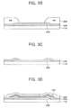
- FIGS. 3A to 3D are cross-sectional views of sequential processes for explaining a method of fabricating an OLED in accordance with the present invention.
- the substrate 110 may use a transparent insulating substrate such as glass, plastic, and quartz.
- a first electrode 320 is formed on the substrate 110.
- the first electrode 320 may be a reflection electrode having at least two layers including transparent layer and reflection layer on the transparent layer, wherein the reflection layer is made of metal having high reflection characteristics.
- the first electrode 320 may be formed of a thin transparent electrode or a thick reflection electrode made of one material selected from a group consisting of Mg, Ca, Al, Ag and an alloy thereof as conductive material having a low work function.
- the first electrode 320 may be deposited by a sputtering method or an ion plating method. More preferably, the first electrode 320 may be deposited by the sputtering method, and then may be formed by selectively patterning using a photoresist (PR) as a mask through a wet etching method, wherein the photoresist (PR) is patterned in a photolithography process.
- PR photoresist
- an inorganic pixel defining layer 330 is formed on the substrate including the first electrode 320.
- the inorganic pixel defining layer 330 functions to define a unit pixel region.
- the present invention uses an inorganic material to form the inorganic pixel defining layer 330.
- the inorganic material for forming the inorganic pixel defining layer 330 may use one selected from an amorphous silicon layer, a silicon oxide layer, a silicon nitride layer, and a silicon oxynitride layer.
- the inorganic pixel defining layer 330 is formed by a deposition method.
- the deposition method for forming a thin layer generally uses a CVD or PVD method.
- the CVD method is a method of obtaining a thin layer made of a desired material through chemical reaction, which may be used to from the inorganic pixel defining layer.
- ambient temperature reaction gas is introduced into a reaction chamber.
- the reaction gas is heated until it arrives to a deposition surface, and heat is continuously supplied to the reaction gas by convection or heating of the deposition surface.
- the reaction gas may generate regular reaction in vapor before it arrives to the deposition surface. Since a gas flow is heated, speed is lowered due to viscosity.
- interface layers of heat, momentum, and chemical composition are formed.
- the introduced gas or reaction intermediate (generated due to vapor thermal decomposition) generates irregular reaction at the deposition surface, thereby forming a thin layer.
- vapor byproducts are discharged from the reaction chamber.
- the inorganic pixel defining layer 330 may be formed using the CVD method.
- the CVD method may be classified into various methods, i.e., atmospheric pressure CVD (APCVD) and low pressure CVD (LPCVD) depending on pressure in the reaction chamber, and the APCVD may be classified into low temperature CVD (LTCVD) and high temperature CVD (HTCVD) depending on performed temperature regions. And otherwise, plasma CVD (PECVD), photo CVD (PHCVD) and so on may be used.
- the PVD method is a method of applying energy to a substrate or a gob made of thin material to physically separate a corresponding material having kinetic energy so that the separated material is deposited on another substrate to form a thin layer, which may be classified into sputtering and vacuum deposition.
- the sputtering method is a method of colliding high-energy particles to a substrate made of the same material as a desired thin layer to separate an atom and a molecule, thereby forming a thin layer.
- the vacuum deposition method is a method of heating a material, which is to be deposited, in a vacuum vessel to increase vapor pressure to thereby deposit the material on a substrate.
- the inorganic pixel defining layer 330 may be formed by the PVD method.
- the present invention is characterized in that the inorganic pixel defining layer 330 is formed by the deposition method.
- the inorganic pixel defining layer 330 formed by the deposition method may be formed to a thickness of 100 - 3000 ⁇ .
- the inorganic pixel defining layer 330 is formed to a small thickness of 100 - 1000 ⁇ , and may be formed to a thickness of 100 ⁇ .
- the inorganic pixel defining layer 330 is patterned to form an opening for exposing at least a portion of the first electrode 320.
- the inorganic pixel defining layer 330 may be patterned by a dry or wet etching method.
- the dry etching method is a method of etching using a physical method by ion impact, or a method applied a chemical action of reaction materials generated in plasma, or a method simultaneously applied a chemical and a physical phenomenon as a chemical action made by ions, electrons and photons.
- the inorganic pixel defining layer 330 is selectively removed by an etching process using a photoresist pattern 340 formed in a photolithography process to be transferred and formed on the substrate in a pattern designed in a reticle.
- the dry etching method is performed by a plasma etching method of plasma discharging the reaction gas in a certain pressure of chamber to decompose into ions, radicals, and electrons, and of causing the radicals generated at this time to generate chemical reaction and the resulting etching action.
- the wet etching method is a method of removing the inorganic pixel defining layer 330 corresponding to the photoresist pattern 340 using a chemical solution, which may use a dipping method, a spray method, and a composite method.
- an organic layer pattern 340 including at least an emission layer is formed on the first electrode 320 and both ends of the inorganic pixel defining layer 330 having an opening.
- the organic layer pattern 340 may be formed using various methods such as inkjet printing, LITI (laser induced thermal imaging), spin coating, deposition, and so on.
- the organic layer pattern 340 is formed using the LITI method.
- a donor substrate (not shown) having an organic layer is laminated on the entire surface of the substrate, and then the laser beam is irradiated on a predetermined region of the donor substrate to form the organic layer pattern 340 on the first electrode 320 and both ends of the inorganic pixel defining layer 330 having the opening.
- the inorganic pixel defining layer 330 is formed to a small thickness of 100 - 3000 ⁇ , preferably, 100 - 1000 ⁇ , a step between the first electrode 320 and the inorganic pixel defining layer 330 is formed at a small height to improve transfer efficiency during the process of forming the organic layer pattern 340. That is, since the transfer may be performed using the laser beam having low energy, luminous efficiency and lifetime of the OLED may be increased. In addition, it is possible to prevent the organic layer pattern to be formed from being cut.
- the organic layer pattern 340 includes at least an emission layer, and may further include at least one layer selected from a hole injection layer, a hole transport layer, a hole blocking layer, an electron transport layer, and an electron injection layer in addition to the emission layer.
- a second electrode 350 is formed on the entire surface of the organic layer pattern 340.
- the second electrode 350 may be formed by a vacuum deposition method.
- the first electrode 320 is a transparent electrode as an anode or a reflection electrode having at least two layers including transparent layer and reflection layer on the transparent layer
- the second electrode is a reflection electrode, i.e., a cathode formed on one material selected from a group consisting of Mg, Ca, Al, Ag and an alloy thereof as conductive metal having a low work function
- the first electrode 320 is a cathode
- the second electrode 350 is a transparent electrode, i.e., an anode formed of ITO or IZO.
- an OLED and method of fabricating the same in accordance with the present invention is capable of improving transfer efficiency, improving luminous efficiency of the OLED, and increasing lifetime of the OLED, by forming an inorganic material as a pixel defining layer to a small thickness using a deposition method to closely adhere the first electrode to the organic layer on the donor substrate during the transfer process to thereby enable the transfer process using a laser beam having low energy.
- an advantage of preventing the organic layer pattern from being cut due to the step between the first electrode and the inorganic pixel defining layer is an advantage of preventing the organic layer pattern from being cut due to the step between the first electrode and the inorganic pixel defining layer.
Landscapes
- Engineering & Computer Science (AREA)
- Microelectronics & Electronic Packaging (AREA)
- Manufacturing & Machinery (AREA)
- Electroluminescent Light Sources (AREA)
Abstract
Description
- This application claims priority to and the benefit of Korean Patent Application No. 2004-0076667, filed September 23, 2004, the disclosure of which is incorporated herein by reference in its entirety.
- The present invention relates to an organic light emitting display and method of fabricating the same and, more particularly, to an organic light emitting display including an inorganic pixel defining layer formed using a deposition method and method of fabricating the same.
- An organic light emitting display (OLED) among flat panel displays is an emissive display of electrically exciting organic compound to emit light so that it does not require a backlight unit, unlike LCD. Therefore, the OLED may be fabricated in a lightweight and thin type and by simple processes. In addition, since the OLED may be fabricated at a low temperature and has characteristics of a fast response speed less than 1 ms, low power consumption, a wide viewing angle due to the emissive display, and high contrast, the OLED is attracting public attention as a next generation flat panel display.
- Generally, the OLED includes an organic emission layer between an anode and a cathode so that holes supplied from the anode and electrons supplied from the cathode are recombined in the organic emission layer to create an exciton being a hole-electron pair, and the exciton is returned to a ground state to generate energy, thereby emitting light.
- FIG. 1 is a cross-sectional view of a conventional OLED.
- Referring to FIG. 1, a patterned
anode 120 is formed on asubstrate 110 having a predetermined element. - An organic
pixel defining layer 130 for defining a pixel and made of an insulating material for insulation between organic emission layers is formed on theanode 120. The organicpixel defining layer 130 is made of any one material selected from a group consisting of polyimid (PI), polyamide (PA), acryl resin, benzocyclobuthene (BCB), and phenol resin. - The organic
pixel defining layer 130 may be deposited on the substrate using a spin coating method. The organicpixel defining layer 130 formed by the spin coating method has a thickness of about 1 µm - 2 µm. The organicpixel defining layer 130 is patterned to form an opening, and anorganic layer pattern 140 including an organic emission layer is formed on the organicpixel defining layer 130 in addition to the exposed anode. - A
cathode 150 is formed on the entire surface of theorganic layer pattern 140. - As described above, in the conventional OLED, an organic material as the organic
pixel defining layer 130 has been formed by a spin coating method. In this case, since the organicpixel defining layer 130 is formed to a large thickness of about 1 µm - 2 µm, a problem may occur that the organic layer pattern formed by the following process is cut due to a large step of the anode and the organicpixel defining layer 130. Dotted lines designate a portion where the organic layer pattern may be cut. In addition, since the organicpixel defining layer 130 is thick, it is difficult to closely adhere the anode to the organic layer on a donor substrate to thereby require a laser beam having high energy during a transfer process. Therefore, there are problems of degrading transfer efficiency, lowering luminous efficiency of the OLED, and reducing lifetime of the OLED. - The present invention, therefore, solves aforementioned problems associated with conventional devices by providing an organic light emitting display (OLED) and method of fabricating the same capable of improving transfer efficiency, improving luminous efficiency of the OLED, increasing lifetime of the OLED, and preventing an organic layer pattern to be formed from being cut, by forming an inorganic material as a pixel defining layer to a small thickness using a deposition method.
- In an exemplary embodiment of the present invention, an organic light emitting display includes: a substrate; a first electrode formed on the substrate; an inorganic pixel defining layer formed on the first electrode and having an opening for exposing at least a portion of the first electrode; an organic layer pattern located on the first electrode and both ends of the inorganic pixel defining layer having the opening, and having at least an emission layer; and a second electrode formed on the organic layer pattern, wherein the inorganic pixel defining layer is formed by a deposition method. As a result, the present invention is capable of improving transfer efficiency, improving luminous efficiency of the OLED, increasing lifetime of the OLED, and preventing an organic layer pattern to be formed from being cut.
- In another exemplary embodiment according to the present invention, a method of fabricating an OLED includes: providing a substrate; forming a first electrode on the substrate; forming an inorganic pixel defining layer on the substrate having the first electrode using a deposition method; patterning the inorganic pixel defining layer to form an opening for exposing at least a portion of the first electrode; forming an organic layer pattern having at least an emission layer on the first electrode and both ends of the inorganic pixel defining layer having the opening; and forming a second electrode on the organic layer pattern. The inorganic pixel defining layer may be patterned by a dry or wet etching method.
- The inorganic pixel defining layer may be formed by a chemical vapor deposition (CVD) method or a physical vapor deposition (PVD) method. In addition, the PVD method may employ a sputtering method.
- The inorganic pixel defining layer may be formed to a thickness of 100 - 3000 Å, preferably, 100 ~ 1000 Å. In addition, the inorganic pixel defining layer may be made of any one material selected from a group consisting of an amorphous silicon layer, a silicon oxide layer, a silicon nitride layer, and a silicon oxynitride layer.
- The first electrode may be an anode, and the second electrode may be a cathode, on the contrary, the first electrode may be a cathode, and the second electrode may be an anode.
- The organic layer pattern can be formed by LITI method.
- The above and other features of the present invention will be described in reference to certain exemplary embodiments thereof with reference to the attached drawings in which:
- FIG. 1 is a cross-sectional view of a conventional organic light emitting display (OLED);
- FIG. 2 is a cross-sectional view of an OLED in accordance with the present invention; and
- FIGS. 3A to 3D are cross-sectional views of sequential processes for explaining a method of fabricating an OLED in accordance with the present invention.
- The present invention will now be described more fully hereinafter with reference to the accompanying drawings, in which preferred embodiments of the invention are shown. This invention may, however, be embodied in different forms and should not be construed as limited to the embodiments set forth herein. Like reference numerals designate like elements throughout the specification.
- FIG. 2 is a cross-sectional view of an OLED in accordance with the present invention.
- Referring to FIG. 2, a predetermined element is formed in a
substrate 110, and afirst electrode 220 is patterned and formed on thesubstrate 110. Thesubstrate 110 may use a transparent insulating substrate such as glass, plastic or quartz. - When the first electrode is an anode, the first electrode may be a transparent electrode made of ITO or IZO having a high work function, or a reflection electrode having at least two layers including transparent layer and reflection layer on the transparent layer, wherein the reflection layer is made of metal having high reflection characteristics such as aluminum, aluminum alloy or the like. When the first electrode is a cathode, the first electrode may be a thin transparent electrode or a thick reflection electrode made of one material selected from a group consisting of Mg, Ca, Al, Ag and an alloy thereof, which are conductive metal having a low work function.
- An inorganic
pixel defining layer 230 is formed on the entire surface of the substrate including thefirst electrode 220, and includes an opening for exposing at least a portion of thefirst electrode 220. - The inorganic
pixel defining layer 230 may be made of one material selected from a group consisting of inorganic materials such as an amorphous silicon layer, a silicon oxide layer, a silicon nitride layer, a silicon oxynitride layer, and so on. - At this time, the inorganic
pixel defining layer 230 is formed by a deposition method, for example, a chemical vapor deposition (CVD) method, a physical vapor deposition (PVD) method or the like. In particular, the PVD method preferably employs a sputtering method. The inorganicpixel defining layer 230 may be formed to a small thickness of 100 - 3000 Å using the deposition method. In order to effectively perform the following transfer process, preferably, the inorganicpixel defining layer 230 has a thickness of 3000 Å or less. When the inorganicpixel defining layer 230 has a thickness of 3000 Å or more, problems may occur that an organic layer pattern to be formed is cut, or transfer efficiency is lowered. More preferably, the inorganicpixel defining layer 230 is formed to a thin thickness of 100 - 1000 Å. - An
organic layer pattern 240 including at least an emission layer is formed on thefirst electrode 220 and both ends of the inorganic pixel defining layer having the opening. While theorganic layer pattern 240 is transferred onto thefirst electrode 220 and the inorganicpixel defining layer 230 by irradiating a laser beam, since the inorganic pixel defining layer has a small thickness of 100 - 1000 Å, the first electrode and the donor substrate having the organic layer are more closely adhered during the transfer process, thereby preventing the organic layer pattern from being cut. In addition, since the transfer may be performed using the laser beam having low energy, transfer efficiency is also improved. Detailed description will be explained in conjunction with FIGS. 3A to 3D. - The
organic layer pattern 240 may include at least one layer selected from a hole injection layer, a hole transport layer, a hole blocking layer, an electron transport layer, and an electron injection layer in addition to the emission layer. - A
second electrode 250 is formed on theorganic layer pattern 240. - When the
first electrode 220 is an anode, i.e., a transparent electrode or a reflection electrode having at least two layers including transparent layer and reflection layer on the transparent layer, , thesecond electrode 250 may be formed of a reflection electrode, i.e., a cathode made of one selected from a group consisting of Mg, Ca, Al, Ag and an alloy thereof as conductive metal having a low work function, and when thefirst electrode 220 is a cathode, thesecond electrode 250 may be formed of a transparent electrode, i.e., an anode made of ITO or IZO. - FIGS. 3A to 3D are cross-sectional views of sequential processes for explaining a method of fabricating an OLED in accordance with the present invention.
- Referring to 3A, a
substrate 110 is provided. Thesubstrate 110 may use a transparent insulating substrate such as glass, plastic, and quartz. - Next, a
first electrode 320 is formed on thesubstrate 110. When thefirst electrode 320 is an anode, thefirst electrode 320 may be a reflection electrode having at least two layers including transparent layer and reflection layer on the transparent layer, wherein the reflection layer is made of metal having high reflection characteristics. When thefirst electrode 320 is a cathode, thefirst electrode 320 may be formed of a thin transparent electrode or a thick reflection electrode made of one material selected from a group consisting of Mg, Ca, Al, Ag and an alloy thereof as conductive material having a low work function. - The
first electrode 320 may be deposited by a sputtering method or an ion plating method. More preferably, thefirst electrode 320 may be deposited by the sputtering method, and then may be formed by selectively patterning using a photoresist (PR) as a mask through a wet etching method, wherein the photoresist (PR) is patterned in a photolithography process. - Next, an inorganic
pixel defining layer 330 is formed on the substrate including thefirst electrode 320. The inorganicpixel defining layer 330 functions to define a unit pixel region. - While the conventional art uses an organic material as a pixel defining layer, the present invention uses an inorganic material to form the inorganic
pixel defining layer 330. The inorganic material for forming the inorganicpixel defining layer 330 may use one selected from an amorphous silicon layer, a silicon oxide layer, a silicon nitride layer, and a silicon oxynitride layer. - The inorganic
pixel defining layer 330 is formed by a deposition method. The deposition method for forming a thin layer generally uses a CVD or PVD method. - The CVD method is a method of obtaining a thin layer made of a desired material through chemical reaction, which may be used to from the inorganic pixel defining layer. In the conventional CVD process, ambient temperature reaction gas is introduced into a reaction chamber. The reaction gas is heated until it arrives to a deposition surface, and heat is continuously supplied to the reaction gas by convection or heating of the deposition surface. According to various process conditions, the reaction gas may generate regular reaction in vapor before it arrives to the deposition surface. Since a gas flow is heated, speed is lowered due to viscosity. In addition, by a change of the gas composition, interface layers of heat, momentum, and chemical composition are formed. The introduced gas or reaction intermediate (generated due to vapor thermal decomposition) generates irregular reaction at the deposition surface, thereby forming a thin layer. Next, vapor byproducts are discharged from the reaction chamber. The inorganic
pixel defining layer 330 may be formed using the CVD method. The CVD method may be classified into various methods, i.e., atmospheric pressure CVD (APCVD) and low pressure CVD (LPCVD) depending on pressure in the reaction chamber, and the APCVD may be classified into low temperature CVD (LTCVD) and high temperature CVD (HTCVD) depending on performed temperature regions. And otherwise, plasma CVD (PECVD), photo CVD (PHCVD) and so on may be used. - The PVD method is a method of applying energy to a substrate or a gob made of thin material to physically separate a corresponding material having kinetic energy so that the separated material is deposited on another substrate to form a thin layer, which may be classified into sputtering and vacuum deposition.
- The sputtering method is a method of colliding high-energy particles to a substrate made of the same material as a desired thin layer to separate an atom and a molecule, thereby forming a thin layer. The vacuum deposition method is a method of heating a material, which is to be deposited, in a vacuum vessel to increase vapor pressure to thereby deposit the material on a substrate. The inorganic
pixel defining layer 330 may be formed by the PVD method. - As described above, the present invention is characterized in that the inorganic
pixel defining layer 330 is formed by the deposition method. The inorganicpixel defining layer 330 formed by the deposition method may be formed to a thickness of 100 - 3000 Å. In addition, preferably, the inorganicpixel defining layer 330 is formed to a small thickness of 100 - 1000 Å, and may be formed to a thickness of 100 Å. - Referring to FIGS. 3B and 3C, the inorganic
pixel defining layer 330 is patterned to form an opening for exposing at least a portion of thefirst electrode 320. The inorganicpixel defining layer 330 may be patterned by a dry or wet etching method. - The dry etching method is a method of etching using a physical method by ion impact, or a method applied a chemical action of reaction materials generated in plasma, or a method simultaneously applied a chemical and a physical phenomenon as a chemical action made by ions, electrons and photons.
- The inorganic
pixel defining layer 330 is selectively removed by an etching process using aphotoresist pattern 340 formed in a photolithography process to be transferred and formed on the substrate in a pattern designed in a reticle. Preferably, the dry etching method is performed by a plasma etching method of plasma discharging the reaction gas in a certain pressure of chamber to decompose into ions, radicals, and electrons, and of causing the radicals generated at this time to generate chemical reaction and the resulting etching action. - The wet etching method is a method of removing the inorganic
pixel defining layer 330 corresponding to thephotoresist pattern 340 using a chemical solution, which may use a dipping method, a spray method, and a composite method. - Referring to FIG. 3D, an
organic layer pattern 340 including at least an emission layer is formed on thefirst electrode 320 and both ends of the inorganicpixel defining layer 330 having an opening. Theorganic layer pattern 340 may be formed using various methods such as inkjet printing, LITI (laser induced thermal imaging), spin coating, deposition, and so on. Preferably, theorganic layer pattern 340 is formed using the LITI method. A donor substrate (not shown) having an organic layer is laminated on the entire surface of the substrate, and then the laser beam is irradiated on a predetermined region of the donor substrate to form theorganic layer pattern 340 on thefirst electrode 320 and both ends of the inorganicpixel defining layer 330 having the opening. - At this time, as described above, since the inorganic
pixel defining layer 330 is formed to a small thickness of 100 - 3000 Å, preferably, 100 - 1000 Å, a step between thefirst electrode 320 and the inorganicpixel defining layer 330 is formed at a small height to improve transfer efficiency during the process of forming theorganic layer pattern 340. That is, since the transfer may be performed using the laser beam having low energy, luminous efficiency and lifetime of the OLED may be increased. In addition, it is possible to prevent the organic layer pattern to be formed from being cut. - The
organic layer pattern 340 includes at least an emission layer, and may further include at least one layer selected from a hole injection layer, a hole transport layer, a hole blocking layer, an electron transport layer, and an electron injection layer in addition to the emission layer. - Continuously, a
second electrode 350 is formed on the entire surface of theorganic layer pattern 340. Thesecond electrode 350 may be formed by a vacuum deposition method. When thefirst electrode 320 is a transparent electrode as an anode or a reflection electrode having at least two layers including transparent layer and reflection layer on the transparent layer, , the second electrode is a reflection electrode, i.e., a cathode formed on one material selected from a group consisting of Mg, Ca, Al, Ag and an alloy thereof as conductive metal having a low work function, and when thefirst electrode 320 is a cathode, thesecond electrode 350 is a transparent electrode, i.e., an anode formed of ITO or IZO. - As can be seen from the foregoing, an OLED and method of fabricating the same in accordance with the present invention is capable of improving transfer efficiency, improving luminous efficiency of the OLED, and increasing lifetime of the OLED, by forming an inorganic material as a pixel defining layer to a small thickness using a deposition method to closely adhere the first electrode to the organic layer on the donor substrate during the transfer process to thereby enable the transfer process using a laser beam having low energy. In addition, there is an advantage of preventing the organic layer pattern from being cut due to the step between the first electrode and the inorganic pixel defining layer.
- Although the present invention has been described with reference to certain exemplary embodiments thereof, it will be understood by those skilled in the art that a variety of modifications and variations may be made to the present invention without departing from the spirit or scope of the present invention defined in the appended claims, and their equivalents.
Claims (15)
- An organic light emitting display comprising:a substrate;a first electrode formed on the substrate;an inorganic pixel defining layer formed on the first electrode and having an opening for exposing at least a portion on the first electrode;an organic layer pattern located on the first electrode and both ends of the inorganic pixel defining layer having the opening, and having at least an emission layer; anda second electrode formed on the organic layer pattern,wherein the inorganic pixel defining layer is formed by a deposition method.
- The organic light emitting display according to claim 1, wherein the inorganic pixel defining layer is formed by any one of a chemical vapor deposition (CVD) method and a physical vapor deposition (PVD) method.
- The organic light emitting display according to claim 2, wherein the inorganic pixel defining layer is formed by a sputtering method.
- The organic light emitting display according to claim 1, wherein the inorganic pixel defining layer is formed to a thickness of 100 - 3000 Å.
- The organic light emitting display according to claim 4, wherein the inorganic pixel defining layer is formed to a thickness of 100 - 1000 Å.
- The organic light emitting display according to claim 1, wherein the inorganic pixel defining layer may be made of one material selected from a group consisting of an amorphous silicon layer, a silicon oxide layer, a silicon nitride layer, and a silicon oxynitride layer.
- A method of fabricating an organic light emitting display, comprising:providing a substrate;forming a first electrode on the substrate;forming an inorganic pixel defining layer on the substrate having the first electrode using a deposition method;patterning the inorganic pixel defining layer to form an opening for exposing at least a portion of the first electrode;forming an organic layer pattern having at least an emission layer on the first electrode and both ends of the inorganic pixel defining layer having the opening; andforming a second electrode on the organic layer pattern.
- The method according to claim 7, wherein the inorganic pixel defining layer is formed by any one of a chemical vapor deposition (CVD) method and a physical vapor deposition (PVD) method.
- The method according to claim 8, wherein the inorganic pixel defining layer is formed by a sputtering method.
- The method according to claim 7, wherein the inorganic pixel defining layer is formed to a thickness of 100 - 3000 Å.
- The method according to claim 10, wherein the inorganic pixel defining layer is formed to a thickness of 100 - 1000 Å.
- The method according to claim 7, wherein the inorganic pixel defining layer is made of one material selected from a group consisting of an amorphous silicon layer, a silicon oxide layer, a silicon nitride layer, and a silicon oxynitride layer.
- The method according to claim 7, wherein the inorganic pixel defining layer is patterned by a dry etching method.
- The method according to claim 7, wherein the inorganic pixel defining layer is patterned by a wet etching method.
- The method according to claim 7, the organic layer pattern is formed by LITI method.
Applications Claiming Priority (1)
| Application Number | Priority Date | Filing Date | Title |
|---|---|---|---|
| KR1020040076667A KR100699998B1 (en) | 2004-09-23 | 2004-09-23 | Organic electroluminescent device and manufacturing method thereof |
Publications (1)
| Publication Number | Publication Date |
|---|---|
| EP1641044A1 true EP1641044A1 (en) | 2006-03-29 |
Family
ID=36072985
Family Applications (1)
| Application Number | Title | Priority Date | Filing Date |
|---|---|---|---|
| EP04090511A Ceased EP1641044A1 (en) | 2004-09-23 | 2004-12-23 | Organic light emitting display and method of fabricating the same |
Country Status (5)
| Country | Link |
|---|---|
| US (1) | US7573070B2 (en) |
| EP (1) | EP1641044A1 (en) |
| JP (1) | JP2006093079A (en) |
| KR (1) | KR100699998B1 (en) |
| CN (1) | CN100556222C (en) |
Families Citing this family (25)
| Publication number | Priority date | Publication date | Assignee | Title |
|---|---|---|---|---|
| KR100659757B1 (en) * | 2004-08-25 | 2006-12-19 | 삼성에스디아이 주식회사 | Organic electroluminescent device and manufacturing method thereof |
| KR20060026776A (en) * | 2004-09-21 | 2006-03-24 | 삼성에스디아이 주식회사 | Organic electroluminescent device and manufacturing method thereof |
| US20060197441A1 (en) * | 2005-03-03 | 2006-09-07 | Yaw-Ming Tsai | Array substrates for electroluminescent displays and methods of forming the same |
| KR100700659B1 (en) * | 2005-03-29 | 2007-03-27 | 삼성에스디아이 주식회사 | Organic light emitting display device and manufacturing method |
| KR102381391B1 (en) * | 2015-04-16 | 2022-03-31 | 삼성디스플레이 주식회사 | Display device |
| GB0510282D0 (en) * | 2005-05-20 | 2005-06-29 | Cambridge Display Tech Ltd | Top-electroluminescent devices comprising cathode bus bars |
| EP2044637B1 (en) * | 2006-07-25 | 2015-09-16 | LG Chem, Ltd. | Method of manufacturing organic light emitting device and organic light emitting device manufactured by using the method |
| KR101431466B1 (en) * | 2008-07-30 | 2014-08-22 | 삼성디스플레이 주식회사 | Method for manufacturing organic light emitting device |
| KR100971751B1 (en) * | 2008-10-23 | 2010-07-21 | 삼성모바일디스플레이주식회사 | Organic light emitting display device and manufacturing method |
| KR20110057985A (en) * | 2009-11-25 | 2011-06-01 | 삼성모바일디스플레이주식회사 | Flexible display device and manufacturing method thereof |
| US8922463B2 (en) | 2010-04-26 | 2014-12-30 | Samsung Display Co., Ltd. | Organic light-emitting display apparatus |
| KR101182447B1 (en) * | 2010-06-16 | 2012-09-12 | 삼성디스플레이 주식회사 | Organic light emitting device and manufacturing method thereof |
| KR101193196B1 (en) | 2010-07-07 | 2012-10-19 | 삼성디스플레이 주식회사 | Organic light emitting display apparatus and the manufacturing method thereof |
| KR101923172B1 (en) * | 2011-05-16 | 2018-11-29 | 삼성디스플레이 주식회사 | Organic light emitting display apparatus and the method for manufacturing of the same |
| KR101848883B1 (en) * | 2011-06-28 | 2018-04-16 | 삼성디스플레이 주식회사 | Organic light emitting device and the manufacturing method of thereof |
| KR101941178B1 (en) * | 2012-09-28 | 2019-01-23 | 삼성디스플레이 주식회사 | Organic light emitting display device and method of manufacturing an organic light emitting display device |
| KR20140058745A (en) | 2012-11-05 | 2014-05-15 | 삼성디스플레이 주식회사 | Organic light emitting diode display and manufacturing method thereof |
| CN104742551B (en) * | 2013-12-27 | 2017-08-04 | 昆山维信诺显示技术有限公司 | A kind of organic material printing transferring method in OLED |
| CN106449718B (en) * | 2016-11-15 | 2019-10-18 | 武汉华星光电技术有限公司 | OLED substrate and manufacturing method thereof |
| CN111969121B (en) | 2019-05-20 | 2024-06-25 | 乐金显示有限公司 | Light-emitting display device |
| KR102894202B1 (en) | 2019-08-19 | 2025-12-02 | 삼성디스플레이 주식회사 | Organic light emitting diode display device and manufacturing method thereof |
| CN112542485A (en) * | 2019-09-23 | 2021-03-23 | 台湾积体电路制造股份有限公司 | Display device and manufacturing method thereof |
| DE102020120751A1 (en) * | 2019-09-23 | 2021-03-25 | Taiwan Semiconductor Manufacturing Co., Ltd. | DISPLAY DEVICE AND METHOD OF MANUFACTURING IT |
| KR102975223B1 (en) | 2020-12-02 | 2026-06-09 | 삼성디스플레이 주식회사 | Display device and Method of manufacturing of the display device |
| CN113161499B (en) * | 2021-04-13 | 2022-06-17 | 浙江大学 | Photoelectric device and manufacturing method thereof |
Citations (11)
| Publication number | Priority date | Publication date | Assignee | Title |
|---|---|---|---|---|
| US20020047567A1 (en) * | 2000-09-06 | 2002-04-25 | Yoshimasa Fujita | Organic led display device of active matrix drive type and fabrication method therefor |
| US6506616B1 (en) * | 1999-11-18 | 2003-01-14 | Texas Instruments Incorporated | Photolithographic method for fabricating organic light-emitting diodes |
| US20030080338A1 (en) * | 2001-10-26 | 2003-05-01 | Semiconductor Energy Laboratory Co., Ltd. | Light emitting device |
| US20030094894A1 (en) * | 2001-11-20 | 2003-05-22 | International Business Machines Corporation | Yield enhancement pixel structure for active matrix organic light-emitting diode displays |
| EP1315209A2 (en) * | 2001-11-26 | 2003-05-28 | Samsung SDI Co. Ltd. | Organic EL display device and method of manufacturing the same |
| US20030169242A1 (en) * | 2002-01-24 | 2003-09-11 | Seiko Epson Corporation | Luminous device and electronic appliances |
| US20030234608A1 (en) * | 2002-06-22 | 2003-12-25 | Samsung Sdi Co., Ltd. | Organic electroluminescent device employing multi-layered anode |
| EP1385209A2 (en) * | 2002-07-25 | 2004-01-28 | Semiconductor Energy Laboratory Co., Ltd. | Method of fabricating an organic light emitting device |
| WO2004026002A1 (en) * | 2002-09-11 | 2004-03-25 | Semiconductor Energy Laboratory Co., Ltd. | Light-emitting apparatus and fabrication method of the same |
| WO2004026003A1 (en) * | 2002-09-12 | 2004-03-25 | Toshiba Matsushita Display Technology Co., Ltd. | Organic el display |
| US20040119419A1 (en) * | 2002-12-11 | 2004-06-24 | Kazuhiko Kai | Organic EL display device |
Family Cites Families (14)
| Publication number | Priority date | Publication date | Assignee | Title |
|---|---|---|---|---|
| JP3670923B2 (en) | 1999-02-26 | 2005-07-13 | 三洋電機株式会社 | Color organic EL display device |
| JP3608613B2 (en) | 2001-03-28 | 2005-01-12 | 株式会社日立製作所 | Display device |
| US6686605B2 (en) * | 2001-07-27 | 2004-02-03 | Semiconductor Energy Laboratory Co., Ltd. | Semiconductor device, display device, and method of manufacturing the same |
| US6822264B2 (en) * | 2001-11-16 | 2004-11-23 | Semiconductor Energy Laboratory Co., Ltd. | Light emitting device |
| JP4101511B2 (en) * | 2001-12-27 | 2008-06-18 | 株式会社半導体エネルギー研究所 | Light emitting device and manufacturing method thereof |
| KR100834344B1 (en) * | 2001-12-29 | 2008-06-02 | 엘지디스플레이 주식회사 | Active matrix organic electroluminescent device and manufacturing method thereof |
| US6810919B2 (en) | 2002-01-11 | 2004-11-02 | Seiko Epson Corporation | Manufacturing method for display device, display device, manufacturing method for electronic apparatus, and electronic apparatus |
| JP2003288983A (en) | 2002-01-24 | 2003-10-10 | Semiconductor Energy Lab Co Ltd | Light emitting device, manufacturing method thereof, and manufacturing device |
| JP2003217855A (en) | 2002-01-28 | 2003-07-31 | Matsushita Electric Ind Co Ltd | Electroluminescence display device and method of manufacturing the same |
| KR20020025917A (en) * | 2002-02-15 | 2002-04-04 | 박병주 | Method of Fabricating Organic Electroluminescent Devices |
| KR100968496B1 (en) | 2002-04-15 | 2010-07-07 | 가부시키가이샤 한도오따이 에네루기 켄큐쇼 | Display device and manufacturing method |
| US7109650B2 (en) * | 2002-07-08 | 2006-09-19 | Lg.Philips Lcd Co., Ltd. | Active matrix organic electroluminescent display device and method of fabricating the same |
| US7893438B2 (en) * | 2003-10-16 | 2011-02-22 | Samsung Mobile Display Co., Ltd. | Organic light-emitting display device including a planarization pattern and method for manufacturing the same |
| JP2005134755A (en) * | 2003-10-31 | 2005-05-26 | Seiko Epson Corp | ELECTRO-OPTICAL DEVICE, MANUFACTURING METHOD THEREOF, AND ELECTRONIC DEVICE |
-
2004
- 2004-09-23 KR KR1020040076667A patent/KR100699998B1/en not_active Expired - Lifetime
- 2004-12-22 US US11/017,648 patent/US7573070B2/en not_active Expired - Lifetime
- 2004-12-23 EP EP04090511A patent/EP1641044A1/en not_active Ceased
- 2004-12-27 JP JP2004377994A patent/JP2006093079A/en active Pending
- 2004-12-31 CN CNB2004100104539A patent/CN100556222C/en not_active Expired - Lifetime
Patent Citations (12)
| Publication number | Priority date | Publication date | Assignee | Title |
|---|---|---|---|---|
| US6506616B1 (en) * | 1999-11-18 | 2003-01-14 | Texas Instruments Incorporated | Photolithographic method for fabricating organic light-emitting diodes |
| US20020047567A1 (en) * | 2000-09-06 | 2002-04-25 | Yoshimasa Fujita | Organic led display device of active matrix drive type and fabrication method therefor |
| US20030080338A1 (en) * | 2001-10-26 | 2003-05-01 | Semiconductor Energy Laboratory Co., Ltd. | Light emitting device |
| US20030094894A1 (en) * | 2001-11-20 | 2003-05-22 | International Business Machines Corporation | Yield enhancement pixel structure for active matrix organic light-emitting diode displays |
| EP1315209A2 (en) * | 2001-11-26 | 2003-05-28 | Samsung SDI Co. Ltd. | Organic EL display device and method of manufacturing the same |
| US20030169242A1 (en) * | 2002-01-24 | 2003-09-11 | Seiko Epson Corporation | Luminous device and electronic appliances |
| US20030234608A1 (en) * | 2002-06-22 | 2003-12-25 | Samsung Sdi Co., Ltd. | Organic electroluminescent device employing multi-layered anode |
| EP1385209A2 (en) * | 2002-07-25 | 2004-01-28 | Semiconductor Energy Laboratory Co., Ltd. | Method of fabricating an organic light emitting device |
| WO2004026002A1 (en) * | 2002-09-11 | 2004-03-25 | Semiconductor Energy Laboratory Co., Ltd. | Light-emitting apparatus and fabrication method of the same |
| WO2004026003A1 (en) * | 2002-09-12 | 2004-03-25 | Toshiba Matsushita Display Technology Co., Ltd. | Organic el display |
| US20050023969A1 (en) * | 2002-09-12 | 2005-02-03 | Kazuyoshi Omata | Organic EL display |
| US20040119419A1 (en) * | 2002-12-11 | 2004-06-24 | Kazuhiko Kai | Organic EL display device |
Also Published As
| Publication number | Publication date |
|---|---|
| US7573070B2 (en) | 2009-08-11 |
| KR100699998B1 (en) | 2007-03-26 |
| KR20060027743A (en) | 2006-03-28 |
| CN100556222C (en) | 2009-10-28 |
| JP2006093079A (en) | 2006-04-06 |
| CN1753589A (en) | 2006-03-29 |
| US20060060838A1 (en) | 2006-03-23 |
Similar Documents
| Publication | Publication Date | Title |
|---|---|---|
| US7573070B2 (en) | Organic light emitting display and method of fabricating the same | |
| EP1638154A1 (en) | Organic light emitting display and method of fabricating the same | |
| US12302694B2 (en) | Organic electroluminescent devices | |
| JP3626736B2 (en) | Method for evaporating thin films used in organic electroluminescent displays | |
| EP2251906B1 (en) | Method of fabricating organic light emitting diode display | |
| US20080128686A1 (en) | Organic light emitting display (OLED) and its method of fabrication | |
| KR100659757B1 (en) | Organic electroluminescent device and manufacturing method thereof | |
| US7148624B2 (en) | Uniform deposition of organic layer | |
| WO2018090444A1 (en) | Oled substrate and manufacturing method thereof | |
| EP1544319A2 (en) | Deposition mask | |
| JP2002252082A (en) | Display device and method of manufacturing display device | |
| US20080268567A1 (en) | Method for fabricating organic light emitting display | |
| KR20090065825A (en) | Shadow mask and manufacturing method | |
| CN100546417C (en) | Organic light emitting display and manufacturing method thereof | |
| KR100570998B1 (en) | Organic EL device and method of forming the same | |
| JP2015088604A (en) | Method for manufacturing bored dielectric layer, and method for manufacturing device including bored dielectric layer | |
| TW444235B (en) | Method of fabricating and patterning oleds | |
| WO2012017486A1 (en) | Method for producing light-emitting elements | |
| KR100666565B1 (en) | Organic light emitting display device and manufacturing method thereof | |
| KR100847220B1 (en) | Organic light emitting device having a surface-treated lower electrode | |
| KR100369575B1 (en) | Method of fabricating organic electroluminescent display | |
| Chang et al. | 38.1: Invited Paper: Manufacturing of Passive Matrix OLED‐Organic Light Emitting Display | |
| KR100711877B1 (en) | Light-emitting display device and manufacturing method | |
| KR100700007B1 (en) | Organic light emitting display device with protective film | |
| WO2007142603A1 (en) | An integrated shadow mask and method of fabrication thereof |
Legal Events
| Date | Code | Title | Description |
|---|---|---|---|
| PUAI | Public reference made under article 153(3) epc to a published international application that has entered the european phase |
Free format text: ORIGINAL CODE: 0009012 |
|
| 17P | Request for examination filed |
Effective date: 20050120 |
|
| AK | Designated contracting states |
Kind code of ref document: A1 Designated state(s): AT BE BG CH CY CZ DE DK EE ES FI FR GB GR HU IE IS IT LI LT LU MC NL PL PT RO SE SI SK TR |
|
| AX | Request for extension of the european patent |
Extension state: AL BA HR LV MK YU |
|
| AKX | Designation fees paid |
Designated state(s): DE FR GB |
|
| 17Q | First examination report despatched |
Effective date: 20061130 |
|
| RAP1 | Party data changed (applicant data changed or rights of an application transferred) |
Owner name: SAMSUNG MOBILE DISPLAY CO., LTD. |
|
| RAP1 | Party data changed (applicant data changed or rights of an application transferred) |
Owner name: SAMSUNG DISPLAY CO., LTD. |
|
| RAP1 | Party data changed (applicant data changed or rights of an application transferred) |
Owner name: SAMSUNG DISPLAY CO., LTD. |
|
| STAA | Information on the status of an ep patent application or granted ep patent |
Free format text: STATUS: THE APPLICATION HAS BEEN REFUSED |
|
| 18R | Application refused |
Effective date: 20161112 |