JP4101511B2 - Light emitting device and manufacturing method thereof - Google Patents
Light emitting device and manufacturing method thereof Download PDFInfo
- Publication number
- JP4101511B2 JP4101511B2 JP2001398624A JP2001398624A JP4101511B2 JP 4101511 B2 JP4101511 B2 JP 4101511B2 JP 2001398624 A JP2001398624 A JP 2001398624A JP 2001398624 A JP2001398624 A JP 2001398624A JP 4101511 B2 JP4101511 B2 JP 4101511B2
- Authority
- JP
- Japan
- Prior art keywords
- insulating film
- electrode
- tft
- light
- film
- Prior art date
- Legal status (The legal status is an assumption and is not a legal conclusion. Google has not performed a legal analysis and makes no representation as to the accuracy of the status listed.)
- Expired - Lifetime
Links
- 238000004519 manufacturing process Methods 0.000 title claims description 12
- 150000002894 organic compounds Chemical class 0.000 claims description 72
- 238000000034 method Methods 0.000 claims description 55
- 238000005530 etching Methods 0.000 claims description 47
- 229910010272 inorganic material Inorganic materials 0.000 claims description 37
- 239000011147 inorganic material Substances 0.000 claims description 37
- 239000007789 gas Substances 0.000 claims description 34
- XUIMIQQOPSSXEZ-UHFFFAOYSA-N Silicon Chemical compound [Si] XUIMIQQOPSSXEZ-UHFFFAOYSA-N 0.000 claims description 33
- 229910052710 silicon Inorganic materials 0.000 claims description 33
- 239000010703 silicon Substances 0.000 claims description 33
- 239000011368 organic material Substances 0.000 claims description 32
- IJGRMHOSHXDMSA-UHFFFAOYSA-N Atomic nitrogen Chemical compound N#N IJGRMHOSHXDMSA-UHFFFAOYSA-N 0.000 claims description 30
- 229910052581 Si3N4 Inorganic materials 0.000 claims description 25
- HQVNEWCFYHHQES-UHFFFAOYSA-N silicon nitride Chemical compound N12[Si]34N5[Si]62N3[Si]51N64 HQVNEWCFYHHQES-UHFFFAOYSA-N 0.000 claims description 25
- 238000004544 sputter deposition Methods 0.000 claims description 19
- 229910052757 nitrogen Inorganic materials 0.000 claims description 15
- NIXOWILDQLNWCW-UHFFFAOYSA-N acrylic acid group Chemical group C(C=C)(=O)O NIXOWILDQLNWCW-UHFFFAOYSA-N 0.000 claims description 13
- 239000004642 Polyimide Substances 0.000 claims description 11
- UMIVXZPTRXBADB-UHFFFAOYSA-N benzocyclobutene Chemical compound C1=CC=C2CCC2=C1 UMIVXZPTRXBADB-UHFFFAOYSA-N 0.000 claims description 11
- 229920001721 polyimide Polymers 0.000 claims description 11
- 239000004952 Polyamide Substances 0.000 claims description 7
- 229920002647 polyamide Polymers 0.000 claims description 7
- 238000000576 coating method Methods 0.000 claims description 6
- 238000001312 dry etching Methods 0.000 claims description 6
- 238000001039 wet etching Methods 0.000 claims description 5
- 150000001408 amides Chemical class 0.000 claims description 3
- 239000010408 film Substances 0.000 description 286
- 239000010410 layer Substances 0.000 description 129
- 239000011229 interlayer Substances 0.000 description 60
- 239000012535 impurity Substances 0.000 description 49
- 239000000758 substrate Substances 0.000 description 47
- 239000000463 material Substances 0.000 description 40
- 239000004065 semiconductor Substances 0.000 description 26
- 230000015572 biosynthetic process Effects 0.000 description 22
- VYPSYNLAJGMNEJ-UHFFFAOYSA-N Silicium dioxide Chemical compound O=[Si]=O VYPSYNLAJGMNEJ-UHFFFAOYSA-N 0.000 description 18
- QVGXLLKOCUKJST-UHFFFAOYSA-N atomic oxygen Chemical compound [O] QVGXLLKOCUKJST-UHFFFAOYSA-N 0.000 description 17
- 239000001301 oxygen Substances 0.000 description 17
- 229910052760 oxygen Inorganic materials 0.000 description 17
- 230000008569 process Effects 0.000 description 13
- 229910052814 silicon oxide Inorganic materials 0.000 description 13
- PXHVJJICTQNCMI-UHFFFAOYSA-N Nickel Chemical compound [Ni] PXHVJJICTQNCMI-UHFFFAOYSA-N 0.000 description 10
- 238000007789 sealing Methods 0.000 description 10
- 239000000872 buffer Substances 0.000 description 9
- 230000000903 blocking effect Effects 0.000 description 8
- 238000002425 crystallisation Methods 0.000 description 7
- BASFCYQUMIYNBI-UHFFFAOYSA-N platinum Chemical compound [Pt] BASFCYQUMIYNBI-UHFFFAOYSA-N 0.000 description 7
- 229910052782 aluminium Inorganic materials 0.000 description 6
- 239000003990 capacitor Substances 0.000 description 6
- 230000008025 crystallization Effects 0.000 description 6
- 230000006866 deterioration Effects 0.000 description 6
- 238000005268 plasma chemical vapour deposition Methods 0.000 description 6
- 239000010936 titanium Substances 0.000 description 6
- OAICVXFJPJFONN-UHFFFAOYSA-N Phosphorus Chemical compound [P] OAICVXFJPJFONN-UHFFFAOYSA-N 0.000 description 5
- WUKWITHWXAAZEY-UHFFFAOYSA-L calcium difluoride Chemical compound [F-].[F-].[Ca+2] WUKWITHWXAAZEY-UHFFFAOYSA-L 0.000 description 5
- 229910001634 calcium fluoride Inorganic materials 0.000 description 5
- 239000000460 chlorine Substances 0.000 description 5
- 239000011521 glass Substances 0.000 description 5
- 238000009616 inductively coupled plasma Methods 0.000 description 5
- 239000011159 matrix material Substances 0.000 description 5
- 229910052698 phosphorus Inorganic materials 0.000 description 5
- 239000011574 phosphorus Substances 0.000 description 5
- 229920005989 resin Polymers 0.000 description 5
- 239000011347 resin Substances 0.000 description 5
- 239000000565 sealant Substances 0.000 description 5
- 229910052721 tungsten Inorganic materials 0.000 description 5
- OYLGJCQECKOTOL-UHFFFAOYSA-L barium fluoride Chemical compound [F-].[F-].[Ba+2] OYLGJCQECKOTOL-UHFFFAOYSA-L 0.000 description 4
- 229910001632 barium fluoride Inorganic materials 0.000 description 4
- 239000002585 base Substances 0.000 description 4
- XJHCXCQVJFPJIK-UHFFFAOYSA-M caesium fluoride Chemical compound [F-].[Cs+] XJHCXCQVJFPJIK-UHFFFAOYSA-M 0.000 description 4
- PCHJSUWPFVWCPO-UHFFFAOYSA-N gold Chemical compound [Au] PCHJSUWPFVWCPO-UHFFFAOYSA-N 0.000 description 4
- 239000010931 gold Substances 0.000 description 4
- 239000011810 insulating material Substances 0.000 description 4
- 150000002500 ions Chemical class 0.000 description 4
- 229910052759 nickel Inorganic materials 0.000 description 4
- 230000000737 periodic effect Effects 0.000 description 4
- 238000000206 photolithography Methods 0.000 description 4
- 229910052719 titanium Inorganic materials 0.000 description 4
- MWUXSHHQAYIFBG-UHFFFAOYSA-N Nitric oxide Chemical compound O=[N] MWUXSHHQAYIFBG-UHFFFAOYSA-N 0.000 description 3
- 239000000956 alloy Substances 0.000 description 3
- XAGFODPZIPBFFR-UHFFFAOYSA-N aluminium Chemical compound [Al] XAGFODPZIPBFFR-UHFFFAOYSA-N 0.000 description 3
- 229910021417 amorphous silicon Inorganic materials 0.000 description 3
- 239000003795 chemical substances by application Substances 0.000 description 3
- 150000001875 compounds Chemical class 0.000 description 3
- 238000010586 diagram Methods 0.000 description 3
- 230000000694 effects Effects 0.000 description 3
- 230000001747 exhibiting effect Effects 0.000 description 3
- 238000010438 heat treatment Methods 0.000 description 3
- 238000009413 insulation Methods 0.000 description 3
- 239000004973 liquid crystal related substance Substances 0.000 description 3
- 239000000203 mixture Substances 0.000 description 3
- IBHBKWKFFTZAHE-UHFFFAOYSA-N n-[4-[4-(n-naphthalen-1-ylanilino)phenyl]phenyl]-n-phenylnaphthalen-1-amine Chemical compound C1=CC=CC=C1N(C=1C2=CC=CC=C2C=CC=1)C1=CC=C(C=2C=CC(=CC=2)N(C=2C=CC=CC=2)C=2C3=CC=CC=C3C=CC=2)C=C1 IBHBKWKFFTZAHE-UHFFFAOYSA-N 0.000 description 3
- 238000000059 patterning Methods 0.000 description 3
- 239000004033 plastic Substances 0.000 description 3
- 229920003023 plastic Polymers 0.000 description 3
- 229910052697 platinum Inorganic materials 0.000 description 3
- 229910021420 polycrystalline silicon Inorganic materials 0.000 description 3
- 239000010453 quartz Substances 0.000 description 3
- 230000009467 reduction Effects 0.000 description 3
- 239000002356 single layer Substances 0.000 description 3
- 238000003860 storage Methods 0.000 description 3
- WFKWXMTUELFFGS-UHFFFAOYSA-N tungsten Chemical compound [W] WFKWXMTUELFFGS-UHFFFAOYSA-N 0.000 description 3
- 239000010937 tungsten Substances 0.000 description 3
- XLYOFNOQVPJJNP-UHFFFAOYSA-N water Substances O XLYOFNOQVPJJNP-UHFFFAOYSA-N 0.000 description 3
- XKRFYHLGVUSROY-UHFFFAOYSA-N Argon Chemical compound [Ar] XKRFYHLGVUSROY-UHFFFAOYSA-N 0.000 description 2
- RTAQQCXQSZGOHL-UHFFFAOYSA-N Titanium Chemical compound [Ti] RTAQQCXQSZGOHL-UHFFFAOYSA-N 0.000 description 2
- XLOMVQKBTHCTTD-UHFFFAOYSA-N Zinc monoxide Chemical compound [Zn]=O XLOMVQKBTHCTTD-UHFFFAOYSA-N 0.000 description 2
- 230000001133 acceleration Effects 0.000 description 2
- 229910052783 alkali metal Inorganic materials 0.000 description 2
- 150000001340 alkali metals Chemical class 0.000 description 2
- 229910045601 alloy Inorganic materials 0.000 description 2
- 229910052785 arsenic Inorganic materials 0.000 description 2
- RQNWIZPPADIBDY-UHFFFAOYSA-N arsenic atom Chemical compound [As] RQNWIZPPADIBDY-UHFFFAOYSA-N 0.000 description 2
- 230000008901 benefit Effects 0.000 description 2
- 239000004305 biphenyl Substances 0.000 description 2
- 239000011575 calcium Substances 0.000 description 2
- 239000000969 carrier Substances 0.000 description 2
- 239000011248 coating agent Substances 0.000 description 2
- 239000004020 conductor Substances 0.000 description 2
- 239000013078 crystal Substances 0.000 description 2
- 230000005684 electric field Effects 0.000 description 2
- 230000005281 excited state Effects 0.000 description 2
- 238000000605 extraction Methods 0.000 description 2
- 239000011152 fibreglass Substances 0.000 description 2
- 229910052737 gold Inorganic materials 0.000 description 2
- 230000005525 hole transport Effects 0.000 description 2
- 229910003437 indium oxide Inorganic materials 0.000 description 2
- PJXISJQVUVHSOJ-UHFFFAOYSA-N indium(iii) oxide Chemical compound [O-2].[O-2].[O-2].[In+3].[In+3] PJXISJQVUVHSOJ-UHFFFAOYSA-N 0.000 description 2
- AMGQUBHHOARCQH-UHFFFAOYSA-N indium;oxotin Chemical compound [In].[Sn]=O AMGQUBHHOARCQH-UHFFFAOYSA-N 0.000 description 2
- 238000010030 laminating Methods 0.000 description 2
- 238000005499 laser crystallization Methods 0.000 description 2
- 229910052750 molybdenum Inorganic materials 0.000 description 2
- 229920005591 polysilicon Polymers 0.000 description 2
- 229920002620 polyvinyl fluoride Polymers 0.000 description 2
- 230000004044 response Effects 0.000 description 2
- 238000004528 spin coating Methods 0.000 description 2
- 239000000126 substance Substances 0.000 description 2
- 239000010409 thin film Substances 0.000 description 2
- 238000002834 transmittance Methods 0.000 description 2
- 238000007740 vapor deposition Methods 0.000 description 2
- 125000001637 1-naphthyl group Chemical group [H]C1=C([H])C([H])=C2C(*)=C([H])C([H])=C([H])C2=C1[H] 0.000 description 1
- STTGYIUESPWXOW-UHFFFAOYSA-N 2,9-dimethyl-4,7-diphenyl-1,10-phenanthroline Chemical compound C=12C=CC3=C(C=4C=CC=CC=4)C=C(C)N=C3C2=NC(C)=CC=1C1=CC=CC=C1 STTGYIUESPWXOW-UHFFFAOYSA-N 0.000 description 1
- 229920002799 BoPET Polymers 0.000 description 1
- ZOXJGFHDIHLPTG-UHFFFAOYSA-N Boron Chemical compound [B] ZOXJGFHDIHLPTG-UHFFFAOYSA-N 0.000 description 1
- OYPRJOBELJOOCE-UHFFFAOYSA-N Calcium Chemical compound [Ca] OYPRJOBELJOOCE-UHFFFAOYSA-N 0.000 description 1
- ZAMOUSCENKQFHK-UHFFFAOYSA-N Chlorine atom Chemical compound [Cl] ZAMOUSCENKQFHK-UHFFFAOYSA-N 0.000 description 1
- 229910000881 Cu alloy Inorganic materials 0.000 description 1
- YCKRFDGAMUMZLT-UHFFFAOYSA-N Fluorine atom Chemical compound [F] YCKRFDGAMUMZLT-UHFFFAOYSA-N 0.000 description 1
- GYHNNYVSQQEPJS-UHFFFAOYSA-N Gallium Chemical compound [Ga] GYHNNYVSQQEPJS-UHFFFAOYSA-N 0.000 description 1
- UFHFLCQGNIYNRP-UHFFFAOYSA-N Hydrogen Chemical compound [H][H] UFHFLCQGNIYNRP-UHFFFAOYSA-N 0.000 description 1
- 229910000861 Mg alloy Inorganic materials 0.000 description 1
- 239000005041 Mylar™ Substances 0.000 description 1
- 229910000577 Silicon-germanium Inorganic materials 0.000 description 1
- LEVVHYCKPQWKOP-UHFFFAOYSA-N [Si].[Ge] Chemical compound [Si].[Ge] LEVVHYCKPQWKOP-UHFFFAOYSA-N 0.000 description 1
- 239000002253 acid Substances 0.000 description 1
- 230000003213 activating effect Effects 0.000 description 1
- 230000004913 activation Effects 0.000 description 1
- 229910052784 alkaline earth metal Inorganic materials 0.000 description 1
- 150000001342 alkaline earth metals Chemical class 0.000 description 1
- 239000010405 anode material Substances 0.000 description 1
- 229910052786 argon Inorganic materials 0.000 description 1
- 229910052788 barium Inorganic materials 0.000 description 1
- DSAJWYNOEDNPEQ-UHFFFAOYSA-N barium atom Chemical compound [Ba] DSAJWYNOEDNPEQ-UHFFFAOYSA-N 0.000 description 1
- 229910052796 boron Inorganic materials 0.000 description 1
- 229910052795 boron group element Inorganic materials 0.000 description 1
- 229910052792 caesium Inorganic materials 0.000 description 1
- TVFDJXOCXUVLDH-UHFFFAOYSA-N caesium atom Chemical compound [Cs] TVFDJXOCXUVLDH-UHFFFAOYSA-N 0.000 description 1
- 229910052791 calcium Inorganic materials 0.000 description 1
- 230000003197 catalytic effect Effects 0.000 description 1
- 239000010406 cathode material Substances 0.000 description 1
- 239000000919 ceramic Substances 0.000 description 1
- 229910052801 chlorine Inorganic materials 0.000 description 1
- 239000003086 colorant Substances 0.000 description 1
- 238000004891 communication Methods 0.000 description 1
- 229910052802 copper Inorganic materials 0.000 description 1
- 238000005336 cracking Methods 0.000 description 1
- 238000006356 dehydrogenation reaction Methods 0.000 description 1
- 238000000151 deposition Methods 0.000 description 1
- 230000008021 deposition Effects 0.000 description 1
- 238000005516 engineering process Methods 0.000 description 1
- 239000003822 epoxy resin Substances 0.000 description 1
- 238000001704 evaporation Methods 0.000 description 1
- 230000002349 favourable effect Effects 0.000 description 1
- 230000005669 field effect Effects 0.000 description 1
- 229910052731 fluorine Inorganic materials 0.000 description 1
- 239000011737 fluorine Substances 0.000 description 1
- 229910052733 gallium Inorganic materials 0.000 description 1
- 230000005283 ground state Effects 0.000 description 1
- 239000001257 hydrogen Substances 0.000 description 1
- 229910052739 hydrogen Inorganic materials 0.000 description 1
- 239000011261 inert gas Substances 0.000 description 1
- 238000005468 ion implantation Methods 0.000 description 1
- 238000001659 ion-beam spectroscopy Methods 0.000 description 1
- UEEXRMUCXBPYOV-UHFFFAOYSA-N iridium;2-phenylpyridine Chemical compound [Ir].C1=CC=CC=C1C1=CC=CC=N1.C1=CC=CC=C1C1=CC=CC=N1.C1=CC=CC=C1C1=CC=CC=N1 UEEXRMUCXBPYOV-UHFFFAOYSA-N 0.000 description 1
- 230000001678 irradiating effect Effects 0.000 description 1
- 229910052747 lanthanoid Inorganic materials 0.000 description 1
- 150000002602 lanthanoids Chemical class 0.000 description 1
- 238000004518 low pressure chemical vapour deposition Methods 0.000 description 1
- 239000011777 magnesium Substances 0.000 description 1
- 230000007246 mechanism Effects 0.000 description 1
- 229910052751 metal Inorganic materials 0.000 description 1
- 239000002184 metal Substances 0.000 description 1
- 230000003287 optical effect Effects 0.000 description 1
- 230000003071 parasitic effect Effects 0.000 description 1
- 230000002093 peripheral effect Effects 0.000 description 1
- 239000012466 permeate Substances 0.000 description 1
- 229920000647 polyepoxide Polymers 0.000 description 1
- 229920000728 polyester Polymers 0.000 description 1
- 229920000642 polymer Polymers 0.000 description 1
- 230000001681 protective effect Effects 0.000 description 1
- 238000004151 rapid thermal annealing Methods 0.000 description 1
- 229910052761 rare earth metal Inorganic materials 0.000 description 1
- 150000002910 rare earth metals Chemical class 0.000 description 1
- 238000005546 reactive sputtering Methods 0.000 description 1
- 230000006798 recombination Effects 0.000 description 1
- 238000005215 recombination Methods 0.000 description 1
- 238000002310 reflectometry Methods 0.000 description 1
- SBEQWOXEGHQIMW-UHFFFAOYSA-N silicon Chemical compound [Si].[Si] SBEQWOXEGHQIMW-UHFFFAOYSA-N 0.000 description 1
- 239000000377 silicon dioxide Substances 0.000 description 1
- 229910052709 silver Inorganic materials 0.000 description 1
- 239000007790 solid phase Substances 0.000 description 1
- 239000000243 solution Substances 0.000 description 1
- 125000006850 spacer group Chemical group 0.000 description 1
- 208000024891 symptom Diseases 0.000 description 1
- 229910052715 tantalum Inorganic materials 0.000 description 1
- MZLGASXMSKOWSE-UHFFFAOYSA-N tantalum nitride Chemical compound [Ta]#N MZLGASXMSKOWSE-UHFFFAOYSA-N 0.000 description 1
- 229920001187 thermosetting polymer Polymers 0.000 description 1
- 229910052723 transition metal Inorganic materials 0.000 description 1
- 150000003624 transition metals Chemical class 0.000 description 1
- TVIVIEFSHFOWTE-UHFFFAOYSA-K tri(quinolin-8-yloxy)alumane Chemical compound [Al+3].C1=CN=C2C([O-])=CC=CC2=C1.C1=CN=C2C([O-])=CC=CC2=C1.C1=CN=C2C([O-])=CC=CC2=C1 TVIVIEFSHFOWTE-UHFFFAOYSA-K 0.000 description 1
- 239000012808 vapor phase Substances 0.000 description 1
- YVTHLONGBIQYBO-UHFFFAOYSA-N zinc indium(3+) oxygen(2-) Chemical compound [O--].[Zn++].[In+3] YVTHLONGBIQYBO-UHFFFAOYSA-N 0.000 description 1
Images


Classifications
-
- H—ELECTRICITY
- H05—ELECTRIC TECHNIQUES NOT OTHERWISE PROVIDED FOR
- H05B—ELECTRIC HEATING; ELECTRIC LIGHT SOURCES NOT OTHERWISE PROVIDED FOR; CIRCUIT ARRANGEMENTS FOR ELECTRIC LIGHT SOURCES, IN GENERAL
- H05B33/00—Electroluminescent light sources
- H05B33/12—Light sources with substantially two-dimensional radiating surfaces
- H05B33/22—Light sources with substantially two-dimensional radiating surfaces characterised by the chemical or physical composition or the arrangement of auxiliary dielectric or reflective layers
-
- H—ELECTRICITY
- H01—ELECTRIC ELEMENTS
- H01L—SEMICONDUCTOR DEVICES NOT COVERED BY CLASS H10
- H01L27/00—Devices consisting of a plurality of semiconductor or other solid-state components formed in or on a common substrate
- H01L27/02—Devices consisting of a plurality of semiconductor or other solid-state components formed in or on a common substrate including semiconductor components specially adapted for rectifying, oscillating, amplifying or switching and having at least one potential-jump barrier or surface barrier; including integrated passive circuit elements with at least one potential-jump barrier or surface barrier
- H01L27/12—Devices consisting of a plurality of semiconductor or other solid-state components formed in or on a common substrate including semiconductor components specially adapted for rectifying, oscillating, amplifying or switching and having at least one potential-jump barrier or surface barrier; including integrated passive circuit elements with at least one potential-jump barrier or surface barrier the substrate being other than a semiconductor body, e.g. an insulating body
- H01L27/1214—Devices consisting of a plurality of semiconductor or other solid-state components formed in or on a common substrate including semiconductor components specially adapted for rectifying, oscillating, amplifying or switching and having at least one potential-jump barrier or surface barrier; including integrated passive circuit elements with at least one potential-jump barrier or surface barrier the substrate being other than a semiconductor body, e.g. an insulating body comprising a plurality of TFTs formed on a non-semiconducting substrate, e.g. driving circuits for AMLCDs
- H01L27/124—Devices consisting of a plurality of semiconductor or other solid-state components formed in or on a common substrate including semiconductor components specially adapted for rectifying, oscillating, amplifying or switching and having at least one potential-jump barrier or surface barrier; including integrated passive circuit elements with at least one potential-jump barrier or surface barrier the substrate being other than a semiconductor body, e.g. an insulating body comprising a plurality of TFTs formed on a non-semiconducting substrate, e.g. driving circuits for AMLCDs with a particular composition, shape or layout of the wiring layers specially adapted to the circuit arrangement, e.g. scanning lines in LCD pixel circuits
-
- H—ELECTRICITY
- H10—SEMICONDUCTOR DEVICES; ELECTRIC SOLID-STATE DEVICES NOT OTHERWISE PROVIDED FOR
- H10K—ORGANIC ELECTRIC SOLID-STATE DEVICES
- H10K59/00—Integrated devices, or assemblies of multiple devices, comprising at least one organic light-emitting element covered by group H10K50/00
- H10K59/10—OLED displays
- H10K59/12—Active-matrix OLED [AMOLED] displays
- H10K59/123—Connection of the pixel electrodes to the thin film transistors [TFT]
-
- H—ELECTRICITY
- H10—SEMICONDUCTOR DEVICES; ELECTRIC SOLID-STATE DEVICES NOT OTHERWISE PROVIDED FOR
- H10K—ORGANIC ELECTRIC SOLID-STATE DEVICES
- H10K59/00—Integrated devices, or assemblies of multiple devices, comprising at least one organic light-emitting element covered by group H10K50/00
- H10K59/10—OLED displays
- H10K59/12—Active-matrix OLED [AMOLED] displays
- H10K59/124—Insulating layers formed between TFT elements and OLED elements
-
- H—ELECTRICITY
- H10—SEMICONDUCTOR DEVICES; ELECTRIC SOLID-STATE DEVICES NOT OTHERWISE PROVIDED FOR
- H10K—ORGANIC ELECTRIC SOLID-STATE DEVICES
- H10K59/00—Integrated devices, or assemblies of multiple devices, comprising at least one organic light-emitting element covered by group H10K50/00
- H10K59/80—Constructional details
- H10K59/87—Passivation; Containers; Encapsulations
- H10K59/873—Encapsulations
- H10K59/8731—Encapsulations multilayered coatings having a repetitive structure, e.g. having multiple organic-inorganic bilayers
-
- H—ELECTRICITY
- H10—SEMICONDUCTOR DEVICES; ELECTRIC SOLID-STATE DEVICES NOT OTHERWISE PROVIDED FOR
- H10K—ORGANIC ELECTRIC SOLID-STATE DEVICES
- H10K50/00—Organic light-emitting devices
- H10K50/80—Constructional details
- H10K50/84—Passivation; Containers; Encapsulations
- H10K50/844—Encapsulations
Description
【0001】
【発明の属する技術分野】
本発明は、一対の電極間に有機化合物を含む膜(以下、「有機化合物層」と記す)を設けた素子に電界を加えることで、蛍光又は燐光が得られる発光素子を用いた発光装置及びその作製方法に関する。なお、本明細書中における発光装置とは、画像表示デバイス、発光デバイス、もしくは光源を指す。また、発光装置にコネクター、例えばFPC(Flexible printed circuit)もしくはTAB(Tape Automated Bonding)テープもしくはTCP(Tape Carrier Package)が取り付けられたモジュール、TABテープやTCPの先にプリント配線板が設けられたモジュール、または発光素子にCOG(Chip On Glass)方式によりIC(集積回路)が直接実装されたモジュールも全て発光装置に含むものとする。
【0002】
【従来の技術】
近年、基板上にTFTを形成する技術が大幅に進歩し、アクティブマトリクス型表示装置への応用開発が進められている。特に、ポリシリコン膜を用いたTFTは、従来のアモルファスシリコン膜を用いたTFTよりも電界効果移動度(モビリティともいう)が高いため高速動作が可能である。
【0003】
このようなアクティブマトリクス型表示装置は、同一基板上に様々な回路や素子を作り込むことで製造コストの低減、表示装置の小型化、歩留まりの上昇、スループットの低減など、様々な利点が得られるとして注目されている。
【0004】
中でも、陽極と有機化合物層と陰極とからなる発光素子をマトリクス状に配置した表示装置(以下、アクティブマトリクス型発光装置と呼ぶ)は、各画素のそれぞれにTFTからなるスイッチング素子(以下、スイッチング用TFTという)を設け、そのスイッチング用TFTによって電流制御を行う駆動素子(以下、電流制御用TFTという)を動作させて発光素子を発光させるというものである。
【0005】
なお、発光素子は、電界を加えることにより発光する素子である。その発光機構は、電極間に有機化合物層を挟んで電圧を印加することにより、陰極から注入された電子および陽極から注入された正孔が有機化合物層中で再結合して、励起状態の分子(以下、分子励起子という)を形成し、その分子励起子が基底状態に戻る際にエネルギーを放出して発光すると言われている。
【0006】
このような発光素子において、通常、有機化合物層は1μmを下回るほどの薄膜で形成される。また、発光素子は、有機化合物層そのものが光を放出する自発光型の素子であるため、従来の液晶ディスプレイに用いられているようなバックライトも必要ない。したがって、発光素子は極めて薄型軽量に作製できることが大きな利点である。
【0007】
こういった薄型軽量・高速応答性・直流低電圧駆動などの特性から、発光素子は次世代のフラットパネルディスプレイ素子として注目されている。また、自発光型であり視野角が広いことから、視認性も比較的良好であり、電気器具の表示画面に用いる素子として有効と考えられているが、以下の点が問題になっていた。
【0008】
通常、基板上にTFTが画素1つに対して少なくとも1つ又は2つ設けられ、さらにTFTを選択して、ONするためにソース信号線およびゲート信号線が形成されている。そして、TFTと、発光素子とを絶縁するためにTFT上に酸化珪素や、窒化珪素などの絶縁材料からなる層間絶縁膜が形成されるが、TFTの厚さは、0.2〜1μmと凹凸があるので、これを避けて画素電極を形成しなければならなかった。なお、このような場合には、実質的に画素電極を形成する領域が小さくなるために画素部の開口率が低下するという問題があった。
【0009】
これに対して、特開平10−189252号公報では、スピンコーティング法により成膜したポリイミドコーティング膜や、シリカにポリマーコーティングを行った後、エッチバック法を用いて形成した膜を用いてTFT上に層間絶縁膜を形成することにより平坦化を行い、さらにその上に発光素子を形成することにより発光装置の開口率を向上させる技術が開示されている。
【0010】
【発明が解決しようとする課題】
ところで、このような発光装置は、基板上に形成されたTFTと層間絶縁膜を介して電気的に接続される構造を有する。なお、層間絶縁膜を形成する材料としては、酸化珪素、窒化珪素、酸化窒化珪素といった珪素を含む無機材料や、ポリイミド、ポリアミド、アクリルといった有機樹脂等の有機材料により形成される。
【0011】
無機材料は、酸素や水分を透過させないという特性を持つが、膜厚が厚くなるとクラックを生じる等の欠点を有する。
【0012】
これに対して、有機材料は、膜厚を厚く形成することができるとともに平坦性に優れていることからTFT上を平坦化するための膜としては非常に適しているが、酸素を透過し、水分を透過もしくは吸収するという欠点を有している。
【0013】
なお、発光素子を形成する有機化合物層は、酸素や水分にきわめて弱いため、すぐに劣化してしまうという欠点を有している。すなわち、酸素や水は発光素子の劣化の原因となり、ダークスポット等の劣化の原因となる。
【0014】
さらに、有機材料からなる第2の層間絶縁膜と、無機材料からなる第3の層間絶縁膜とを積層した場合において、積層膜のパターニングを良好に行うために技術的な困難を生じる。具体的には、上記積層膜を成膜した後で、TFTと発光素子の電極を接続する配線形成のためのコンタクトホールを形成すると、コンタクトホールの端部であり、第1の層間絶縁膜と第2の層間絶縁膜とが積層されている断面が露出している部分で、第3の層間絶縁膜が膜剥がれ(もしくは、ピーリング)を起こすといった問題がある。
【0015】
そこで本発明では、TFTと発光素子の間に形成される層間絶縁膜に含まれる水や酸素により発光素子が劣化するのを防ぐ構造を提供すると共に、無機材料からなる絶縁膜と有機材料からなる絶縁膜とを積層した際に生じる問題を解決することを目的とする。
【0016】
【課題を解決するための手段】
本発明では、基板上に形成されたTFTの上に無機材料からなる無機絶縁膜で第1の絶縁膜を形成し、第1の絶縁膜上に有機材料からなる有機絶縁膜で第2の絶縁膜を形成し、第2の絶縁膜上に無機材料からなる無機絶縁膜で第3の絶縁膜を積層し、第3の絶縁膜上に陽極、有機化合物層、および陰極からなる発光素子を形成することを特徴とする。
【0017】
さらに、本発明では第2の絶縁膜と第3の絶縁膜とを積層して、第2の絶縁膜からの水分及び酸素の放出を防ぐ構造とするだけでなく、コンタクトホールが形成される部分には、第3の絶縁膜が積層されないような構造とすることを特徴とする。
【0018】
具体的には、第1の絶縁膜と第2の絶縁膜と第3の絶縁膜とを積層して形成した後、発光素子の第1の電極となる導電膜を成膜し、第1の電極を形成するパターニングの際に、第3の絶縁膜も部分的にエッチングし、エッチングにより表面が露呈している第2の絶縁膜、第1の絶縁膜およびゲート絶縁膜にコンタクトホールが形成される。
【0019】
本発明において開示する発明の構成は、絶縁表面上に形成されたTFTと、前記TFT上に形成された無機材料からなる第1の絶縁膜と、前記第1の絶縁膜上に形成された有機材料からなる第2の絶縁膜と、第1の電極、有機化合物層、および第2の電極からなる発光素子とを有する発光装置であって、前記第1の電極と重なる位置に無機材料からなる第3の絶縁膜を有することを特徴とする発光装置である。
【0020】
また、他の発明の構成は、絶縁表面上に形成されたTFTと、前記TFT上に形成された無機材料からなる第1の絶縁膜と、前記第1の絶縁膜上に形成された有機材料からなる第2の絶縁膜と、前記第1の絶縁膜及び前記第2の絶縁膜において形成されたコンタクトホールと、第1の電極、有機化合物層、および第2の電極からなる発光素子と、前記第2の絶縁膜および前記第1の電極に挟まれ、かつ前記第1の電極と重なる位置に形成された無機材料からなる第3の絶縁膜とを有する発光装置であって、前記TFTは、前記コンタクトホールに形成された配線を介して前記第1の電極と電気的に接続されることを特徴とする発光装置である。
【0021】
また、他の発明の構成は、絶縁表面上に形成されたTFTと、前記TFT上に形成された無機材料からなる第1の絶縁膜と、前記第1の絶縁膜上に形成された有機材料からなる第2の絶縁膜と、前記TFTが有するゲート絶縁膜、前記第1の絶縁膜、および前記第2の絶縁膜において形成されたコンタクトホールと、第1の電極、有機化合物層、および第2の電極からなる発光素子と、前記第2の絶縁膜および前記第1の電極に挟まれ、かつ前記第1の電極と重なる位置に形成された無機材料からなる第3の絶縁膜とを有する発光装置であって、前記コンタクトホールにおいて、前記第1の絶縁膜、前記第2の絶縁膜およびゲート絶縁膜と接して形成された配線を有し、前記配線は、前記TFTと前記第1の電極とを電気的に接続することを特徴とする発光装置である。
【0022】
なお、上記各構成において、無機材料としては、窒化酸化珪素膜、窒化珪素膜を用いることができ、珪素の含有比率が25.0atomic%以上35.0atomic%以下であり、窒素の含有比率が35.0atomic%以上65.0atomic%以下であることが望ましい。なお、酸化珪素膜を用いることもできるが、アルカリ金属などのブロッキング性の面を考慮すると窒化酸化珪素膜又は窒化珪素膜を用いるのが好ましい。
【0023】
なお、上記各構成において、有機材料としては、熱硬化型又は光硬化型の有機樹脂材料を用いることができ、アクリル、ポリイミド、ポリアミド、ポリイミドアミド、BCB(ベンゾシクロブテン)等を用いることができる。
【0024】
また、本発明における他の構成は、絶縁表面上にTFTを形成し、前記TFT上にスパッタリング法により無機材料からなる第1の絶縁膜を形成し、前記第1の絶縁膜上に塗布法により有機材料からなる第2の絶縁膜を形成し、前記第2の絶縁膜上にスパッタリング法により無機材料からなる第3の絶縁膜を形成し、前記第3の絶縁膜上に発光素子の第1の電極となる導電膜を形成し、マスクを用いた第1のエッチングにより、前記導電膜から第1の電極を形成し、第2のエッチングにより前記第1の電極と重なる部分を残して前記第3の絶縁膜を除去することを特徴とする発光装置の作製方法である。
【0025】
さらに、本発明における他の構成は、絶縁表面上にTFTを形成し、前記TFT上にスパッタリング法により無機材料からなる第1の絶縁膜を形成し、前記第1の絶縁膜上に塗布法により有機材料からなる第2の絶縁膜を形成し、前記第2の絶縁膜上にスパッタリング法により無機材料からなる第3の絶縁膜を形成し、前記第3の絶縁膜上に発光素子の第1の電極となる導電膜を形成し、マスクを用いた第1のエッチングにより、前記導電膜から第1の電極を形成し、第2のエッチングにより前記第1の電極と重なる部分を残して前記第3の絶縁膜を除去し、前記第1の絶縁膜、前記第2の絶縁膜および前記TFTが有するゲート絶縁膜において、コンタクトホールを形成し、前記コンタクトホールに配線を形成し、前記配線を前記TFTおよび前記第1の電極と接して形成し、前記第1の電極上に有機化合物層を形成し、前記有機化合物層上に発光素子の第2の電極を形成することを特徴とする発光装置の作製方法である。
【0026】
上記各構成において、無機材料の成膜法として、スパッタリング法、反応性スパッタリング法、イオンビームスパッタリング法、ECR(電子サイクロトロン共鳴)スパッタリング法、イオン化蒸着法等の気相成膜法を用いることができる。なお、これらの成膜方法は、いずれも物理的に原子又は分子を基板上に被着させる方法なので、先に形成されている有機材料からなる層間絶縁膜と殆ど反応せず、化学的に変質させてしまう恐れがない。また、室温〜300℃の温度範囲であっても緻密な膜を形成できるという特徴がある。そして、酸素や水分の透過を阻止する特性を有している。
【0027】
なお、上記スパッタリング法を用いる場合には、室温〜300℃の基板温度において、光透過率の良好な珪素及び窒素を主成分とする無機絶縁膜を形成することができる。この無機絶縁膜を有機材料からなる層間絶縁膜と、陽極、陰極及び有機化合物層からなる発光素子との間に設けることにより、有機材料からなる層間絶縁膜から酸素や水分が放出されるのを遮蔽することができるので発光素子の劣化を防止することができる。
【0028】
なお、前記珪素及び窒素を主成分とする無機絶縁膜をスパッタリング法により成膜する場合には、珪素を主成分とするターゲットを用い、スパッタガスとして、アルゴン、窒素、酸素、窒素酸化物、を使用して形成する。なお、前記珪素及び窒素を主成分とする無機絶縁膜は、成膜時のガス流量により、窒素と、酸素との組成比が変わる。そこで、本明細書中では、前記組成比において、珪素以外の主成分が窒素である膜を、窒化珪素膜とよび、また、前記組成比において、珪素以外の主成分が酸素および窒素である膜を、酸化窒化珪素膜とよぶことにする。
【0029】
また、前記珪素及び窒素を主成分とする無機絶縁膜を前記スパッタリング法により成膜する場合には、珪素をターゲットとして、希ガスと窒素を含有するガスを用いて成膜を行うことで珪素の含有比率が25.0atomic%以上35.0atomic%以下であり、窒素の含有比率が35.0atomic%以上65.0atomic%以下である膜を形成することができる。
【0030】
以上の工程では、基板を300℃以上に加熱することがないため、樹脂基板、またはフレキシブルな基板材料(プラスチック)上にTFTを形成する場合にも同様に適用することができる。
【0031】
また、上記各構成において、無機材料からなる無機絶縁膜を形成した後、無機絶縁膜上に透明導電膜を形成し、これをフォトリソグラフィーによりマスクを形成し、第1のエッチングを行うことにより第1の電極が形成される。さらに、マスクを除去せずに第2のエッチングを行うことによりマスクと重ならない位置にある無機絶縁膜がエッチングされる。なお、エッチング方法としては、ウエットエッチング法とドライエッチング法があるが、本発明においては、第1のエッチングにはウエットエッチング法を用い、第2のエッチングには、ドライエッチング法を用いる。
【0032】
なお、本発明の発光装置から得られる発光は、一重項励起状態又は三重項励起状態のいずれか一方、またはその両者による発光を含むものとする。
【0033】
【発明の実施の形態】
[実施の形態1]
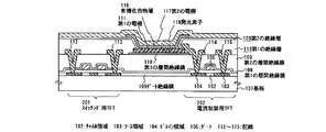
本発明の実施の形態について、図1を用いて説明する。なお、図1には、本発明において、発光装置の画素部に形成される発光素子の断面構造を示す。また、ここで示す発光素子は、有機化合物層で生じた光を基板側(以下に示す、第1の電極側)から取り出す構造(いわゆる、下方出射型)の場合について説明する。
【0034】
図1において、基板101上に薄膜トランジスタ(TFT)が形成されている。なお、ここでは、発光素子118の第1の電極111と電気的に接続され、発光素子118に供給される電流を制御する機能を有する電流制御用TFT202と、電流制御用TFT202のゲート電極106に印加されるビデオ信号を制御するためのスイッチング用TFT201を示している。本実施の形態の場合には、電流制御用TFT202は、pチャネル型TFTで形成され、スイッチング用TFT201は、nチャネル型TFTで形成されている。
【0035】
基板101としては、透光性を有する基板としてガラス基板を用いるが、石英基板や樹脂基板、またはフレキシブルな基板材料(プラスチック)を用いても良い。また、各TFTの活性層は、少なくともチャネル形成領域102、ソース領域103、ドレイン領域104を備えている。
【0036】
また、各TFTの活性層は、ゲート絶縁膜105で覆われ、ゲート絶縁膜105を介してチャネル形成領域102と重なるゲート電極106が形成されている。また、ゲート電極106を覆う第1の層間絶縁膜108が設けられ、その第1の層間絶縁膜108上に第2の層間絶縁膜109が形成され、さらに、第2の層間絶縁膜109上に第3の層間絶縁膜110が形成されている。
【0037】
なお、第1の層間絶縁膜108は、酸化珪素、窒化珪素、窒化酸化珪素および塗布シリコン酸化膜(SOG:Spin On Glass)等の珪素を含む無機材料により形成され、第2の層間絶縁膜109は、ポリイミド、ポリアミド、アクリル(感光性アクリルを含む)、BCB(ベンゾシクロブテン)といった有機材料を用いて形成される。また、第3の層間絶縁膜110は、酸化珪素、窒化珪素、窒化酸化珪素およびSOG等の珪素を含む無機材料により形成される。
【0038】
そして、第3の層間絶縁膜110を形成した後、透明導電膜を形成し、これをパターニングすることにより光取り出し電極である第1の電極111が形成される。
【0039】
なお、本実施の形態においては第1の電極111を陽極として機能する電極とすることから、ここで用いる透明導電膜としては、仕事関数が4.5eV以上の仕事関数の大きい材料を用いる。具体的には、酸化インジウム・スズ(ITO: indium tin oxide)膜、酸化インジウムに2〜20[%]の酸化亜鉛(ZnO)を混合した(IZO:indium zinc oxide)膜、といった透光性の導電膜の他、金(Au)、白金(Pt)、ニッケル(Ni)、タングステン(W)、チタン(Ti)等の長周期型の周期表における3〜11族に属する元素を導電性材料として用いることができる。
【0040】
一方、後から形成される第2の電極が光取り出し電極となる場合には、第1の電極111を透光性の陽極材料により形成する。なお、この場合には、金(Au)、白金(Pt)、ニッケル(Ni)、タングステン(W)、チタン(Ti)等の長周期型の周期表における3〜11族に属する元素を可視光に対する透過率が10%未満となるような膜厚で形成することにより用いることができる。
【0041】
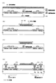
なお、第3の層間絶縁膜110および透明導電膜120が成膜された状態を図2(A)に示す。また、図1と同じものに関しては、共通の記号を用いるものとする。
【0042】
次に、透明導電膜120上にフォトリソグラフィーによりマスク121を形成し、透明導電膜120のエッチングを行う。なお、透明導電膜120のエッチングには、ウエットエッチング法を用いる。これにより第1の電極111がパターン形成される(図2(B))。
【0043】
さらに、マスク121を除去せずにドライエッチング法により、第3の層間絶縁膜110をエッチングする。この時、マスク121で覆われ、第1の電極111と重なる位置に形成されている第3の層間絶縁膜110はエッチングされずに残り、それ以外の部分がエッチングされる(図2(C))。
【0044】
マスク121を除去した後で、第2の層間絶縁膜109、第1の層間絶縁膜108およびゲート絶縁膜105に各TFTのソースまたはドレインに到達するコンタクトホールを形成する。そして、コンタクトホール形成後に各TFTのソース領域またはドレイン領域とを電気的に接続する配線112〜115が形成される(図2(D))。
【0045】
このような工程を経て、図1に示すような構造の第3の層間絶縁膜110を第2の層間絶縁膜109と第1の電極111との間に形成することで、有機材料からなる第2の層間絶縁膜109からの水分や酸素が発光素子118側に放出されるのを無機材料からなる第3の層間絶縁膜110により防ぐことができると共に、第3の層間絶縁膜が除去された第1の層間絶縁膜および第2の層間絶縁膜において、各TFTのソース領域又はドレイン領域に到達するコンタクトホールが形成されるため、第2の層間絶縁膜と第3の層間絶縁膜とが積層部分にコンタクトホールが形成された場合に問題となる膜剥がれを防ぐことができる。
【0046】
なお、第1の電極111は、配線114を介して電流制御用TFT202のドレイン領域104と接続されており、電流制御用TFT202から第1の電極111に供給される電流値により発光素子118における発光輝度が制御される。
【0047】
また、図1に示すように第1の電極111の端部、及び配線(112〜115)は第1の絶縁層119、第2の絶縁層120により覆われている。なお、第1の絶縁層119、第2の絶縁層120を形成する材料としては、酸化珪素、窒化珪素、窒化酸化珪素および塗布シリコン酸化膜(SOG:Spin On Glass)等の珪素を含む無機材料の他、ポリイミド、ポリアミド、アクリル(感光性アクリルを含む)、BCB(ベンゾシクロブテン)といった有機材料からなる絶縁膜を用いる。なお、膜厚は、0.1〜2μmで形成することができるが、特に酸化珪素、窒化珪素および窒化酸化珪素等の珪素を含む材料を用いる場合には0.1〜0.3μmの膜厚で形成することが望ましい。
【0048】
第1の絶縁層119は第1の電極111と重なる位置に開口部を有している。また、第1の絶縁層119上に第2の絶縁層120が形成される。なお、第2の絶縁層120も第1の電極111と重なる位置に開口部を有している。
【0049】
また、第1の電極111(陽極)上には有機化合物層116が形成されており、有機化合物層116上に形成された第2の電極(陰極)117とにより発光素子118が形成される。なお、有機化合物層116を形成する材料としては、低分子系の材料であっても良いし、高分子系の材料であっても良い。また、第2の電極(陰極)117に用いる仕事関数の小さい(具体的には、仕事関数が3.8eV以下)材料としては、元素周期律の1族または2族に属する元素、すなわちアルカリ金属及びアルカリ土類金属、およびこれらを含む合金や化合物の他、希土類金属を含む遷移金属を用いることができる。第2の電極(陰極)117は、蒸着法又はスパッタリング法により形成することができる。
【0050】
本実施の形態1において、第1の電極111に陽極となる透明導電膜を用いることから有機化合物層116におけるキャリアの再結合により生じた光が、第1の電極111側から出射される構造となる。なお、第2の電極117は、遮光性の材料により形成されることが望ましい。
【0051】
また、本実施の形態においては、有機化合物層116と第2の電極117との界面にバッファー層(図示せず)を設ける構造とする。なお、バッファー層を形成する材料としては、フッ化バリウム(BaF2)、フッ化カルシウム(CaF2)、フッ化セシウム(CsF)等を用いることができるが、膜厚を1nm程度で形成する必要がある。その他にもセシウム(Cs)、バリウム(Ba)、カルシウム(Ca)、マグネシウム合金(Mg:Ag)およびランタノイド系の材料を用いることができる。ここでは、フッ化バリウム(BaF2)を1nmの膜厚で成膜してバッファー層を形成する。そして、バッファー層の上に第2の電極117となるAlを100nmの膜厚で成膜する。なお、本実施の形態では、バッファー層を第2の電極117に含めるものとする。
【0052】
以上により、第1の電極111、有機化合物層116、および第2の電極117とからなる発光素子118を有する発光装置を形成することができる。
【0053】
[実施の形態2]
次に、本実施の形態2では、図3〜図6を用いて同一基板上に画素部と、画素部の周辺に設ける駆動回路のTFT(nチャネル型TFT及びpチャネル型TFT)を同時に作製する方法について詳細に説明する。
【0054】
まず、基板600上に下地絶縁膜601を形成し、結晶構造を有する第1の半導体膜を得た後、所望の形状にエッチング処理して島状に分離された半導体層602〜605を形成する。
【0055】
基板600としては、ガラス基板、石英基板、セラミック基板などを用いることができる。また、下地絶縁膜601としては、プラズマCVD法で成膜温度400℃、原料ガスSiH4、NH3、N2Oから作製される酸化窒化珪素膜601aを50nm(好ましくは10〜200nm)形成する。次いで、プラズマCVD法で成膜温度400℃、原料ガスSiH4、N2Oから作製される酸化窒化珪素膜601bを100nm(好ましくは50〜200nm)の厚さに積層形成し、さらにプラズマCVD法で成膜温度300℃、成膜ガスSiH4で非晶質構造を有する半導体膜(ここではアモルファスシリコン膜)を54nmの厚さ(好ましくは25〜80nm)で形成する。
【0056】
本実施の形態では下地膜601を2層構造として示したが、前記絶縁膜の単層膜または2層以上積層させた構造として形成しても良い。また、半導体膜の材料に限定はないが、好ましくはシリコン(珪素)またはシリコンゲルマニウム(SiXGe1-X(X=0.0001〜0.02))合金などを用い、公知の手段(スパッタ法、LPCVD法、またはプラズマCVD法等)により形成すればよい。
【0057】
次いで、非晶質構造を有する半導体膜を結晶化させて結晶構造を有する半導体膜を形成する。なお、ここでの結晶化としては、公知の結晶化技術、例えば固相成長法やレーザー結晶化法を用いることができる。
【0058】
なお、レーザー結晶化を行う場合には、パルス発振型または連続発振型のエキシマレーザーやYAGレーザー、YVO4レーザー、YLFレーザーを用いることができる。YAGレーザー、YVO4レーザー、YLFレーザーを用いる場合には、その第2高調波〜第4高調波を利用する。これらのレーザーを用いる場合には、レーザー発振器から放出されたレーザー光を光学系で線状に集光し半導体膜に照射する方法を用いると良い。結晶化の条件は、実施者が適宜選択すればよい。
【0059】
その他の結晶化法として、ニッケルなどの半導体の結晶化に対し触媒作用のある金属元素を添加して結晶化させても良い。例えば、ニッケルを含有する溶液を非晶質珪素膜上に保持させた後、脱水素化(500℃、1時間)続けて熱結晶化(550℃、4時間)を行い、更に結晶性を向上させるためYAGレーザー、YVO4レーザー、YLFレーザーから選ばれた連続発振レーザー光の第2高調波を照射する。
【0060】
次いで、得られた結晶構造を有する珪素膜(ポリシリコン膜とも呼ばれる)の表面にレジストからなるマスクを形成し、所望の形状にエッチング処理して島状に分離された半導体層602〜605を形成する。半導体層を形成した後、レジストからなるマスクを除去する。
【0061】
また、半導体層を形成した後、TFTのしきい値(Vth)を制御するためにp型あるいはn型を付与する不純物元素を添加してもよい。なお、半導体に対してp型を付与する不純物元素には、ボロン(B)、アルミニウム(Al)、ガリウム(Ga)など周期律第13族元素が知られている。なお、半導体に対してn型を付与する不純物元素としては周期律15族に属する元素、典型的にはリン(P)または砒素(As)が知られている。
【0062】
次いで、半導体層602〜605を覆うゲート絶縁膜607を形成する。ゲート絶縁膜607はプラズマCVD法やスパッタ法で、酸化珪素又は酸化窒化珪素などの無機絶縁体材料を用いて形成し、その厚さを40〜150nmとして珪素を含む絶縁膜で形成する。勿論、このゲート絶縁膜は、珪素を含む絶縁膜を単層或いは積層構造として用いることができる。
【0063】
次いで、図3(A)に示すように、ゲート絶縁膜607上に膜厚20〜100nmの第1の導電膜608と、膜厚100〜400nmの第2の導電膜609とを積層形成する。本実施の形態では、ゲート絶縁膜607上に膜厚30nmの窒化タンタル膜、膜厚370nmのタングステン膜を順次積層する。
【0064】
第1の導電膜及び第2の導電膜を形成する導電性材料としてはTa、W、Ti、Mo、Al、Cuから選ばれた元素、または前記元素を主成分とする合金材料もしくは化合物材料で形成する。なお、第1の導電膜及び第2の導電膜としてリン等の不純物元素をドーピングした多結晶珪素膜に代表される半導体膜や、Ag:Pd:Cu合金を用いてもよい。
【0065】
次に、図3(B)に示すように光露光工程によりレジストからなるマスク610〜613を形成し、ゲート電極及び配線を形成するための第1のエッチング処理を行う。第1のエッチング処理では第1及び第2のエッチング条件で行う。エッチングにはICP(Inductively Coupled Plasma:誘導結合型プラズマ)エッチング法を用いると良い。ICPエッチング法を用い、エッチング条件(コイル型の電極に印加される電力量、基板側の電極に印加される電力量、基板側の電極温度等)を適宜調節することによって所望のテーパー形状に膜をエッチングすることができる。なお、エッチング用ガスとしては、Cl2、BCl3、SiCl4、CCl4などを代表とする塩素系ガスまたはCF4、SF6、NF3などを代表とするフッ素系ガス、またはO2を適宜用いることができる。
【0066】
本実施の形態では、基板側(試料ステージ)にも150WのRF(13.56MHz)電力を投入し、実質的に負の自己バイアス電圧を印加する。なお、基板側の電極面積サイズは、12.5cm×12.5cmであり、コイル型の電極面積サイズ(ここではコイルの設けられた石英円板)は、直径25cmの円板である。
【0067】
本実施例では第1のエッチング条件として、ICP(Inductively Coupled Plasma:誘導結合型プラズマ)エッチング法を用い、エッチング用ガスにCF4とCl2とO2とを用い、それぞれのガス流量比を25/25/10(sccm)とし、1Paの圧力でコイル型の電極に500WのRF(13.56MHz)電力を投入してプラズマを生成してエッチングを行う。基板側(試料ステージ)にも150WのRF(13.56MHz)電力を投入し、実質的に負の自己バイアス電圧を印加する。この第1のエッチング条件によりW膜をエッチングして第1の導電層の端部をテーパー形状とする。
【0068】
この後、レジストからなるマスク610〜613を除去せずに第2のエッチング条件に変え、エッチング用ガスにCF4とCl2とを用い、それぞれのガス流量比を30/30(sccm)とし、1Paの圧力でコイル型の電極に500WのRF(13.56MHz)電力を投入してプラズマを生成して約30秒程度のエッチングを行った。基板側(試料ステージ)にも20WのRF(13.56MHz)電力を投入し、実質的に負の自己バイアス電圧を印加する。CF4とCl2を混合した第2のエッチング条件ではW膜及びTaN膜とも同程度にエッチングされる。
【0069】
こうして、第1のエッチング処理により第1の導電層と第2の導電層から成る第1の形状の導電層615〜618(第1の導電層615a〜618aと第2の導電層615b〜618b)を形成する。ゲート絶縁膜となる絶縁膜607は、10〜20nm程度エッチングされ、第1の形状の導電層615〜618で覆われない領域が薄くなったゲート絶縁膜620となる。
【0070】
次いで、レジストからなるマスクを除去せずに第2のエッチング処理を行う。ここでは、エッチング用ガスにSF6とCl2とO2とを用い、それぞれのガス流量比を24/12/24(sccm)とし、1.3Paの圧力でコイル型の電極に700WのRF(13.56MHz)電力を投入してプラズマを生成してエッチングを行う。基板側(試料ステージ)にも10WのRF(13.56MHz)電力を投入し、実質的に負の自己バイアス電圧を印加する。
【0071】
この第2のエッチング処理により第2の導電層621b〜624bを形成する。一方、第1の導電層は、ほとんどエッチングされず、第1の導電層621a〜624aとなる。なお、第1の導電層621a〜624aは、第1の導電層615a〜618aとほぼ同一サイズである。
【0072】
次いで、レジストからなるマスクを除去した後、第1のドーピング処理を行って図4(A)の状態を得る。ドーピング処理はイオンドープ法、もしくはイオン注入法で行えば良い。イオンドープ法の条件はドーズ量を6.0×10¹³atoms/cm2とし、加速電圧を60〜100keVとして行う。n型を付与する不純物元素として、典型的にはリン(P)または砒素(As)を用いる。この場合、第1の導電層及び第2の導電層621〜624がn型を付与する不純物元素に対するマスクとなり、自己整合的に第1の不純物領域626〜629が形成される。第1の不純物領域626〜629には1×1016〜1×1017/cm3の濃度範囲でn型を付与する不純物元素を添加する。ここでは、第1の不純物領域と同じ濃度範囲の領域をn--領域とも呼ぶ。
【0073】
次いで、図4(B)に示すようにレジストからなるマスク631〜633を形成し第2のドーピング処理を行う。マスク631は駆動回路のpチャネル型TFTを形成する半導体層のチャネル形成領域及びその周辺の領域を保護するマスクであり、マスク632は画素部のTFTを形成する半導体層のチャネル形成領域及びその周辺の領域とを保護するマスクである。
【0074】
第2のドーピング処理におけるイオンドープ法の条件はドーズ量を3.0×10¹⁵atoms/cm2とし、加速電圧を60〜100keVとしてリン(P)をドーピングする。ここでは、第2の導電層621bをマスクとして各半導体層に不純物領域が自己整合的に形成される。勿論、マスク631〜633で覆われた領域には添加されない。こうして、第2の不純物領域634、635と、第3の不純物領域637が形成される。第2の不純物領域634、635には1×1020〜1×1021/cm3の濃度範囲でn型を付与する不純物元素を添加されている。ここでは、第2の不純物領域と同じ濃度範囲の領域をn+領域とも呼ぶ。
【0075】
また、第3の不純物領域は第1の導電層により第2の不純物領域よりも低濃度に形成され、1×10¹⁸〜1×10¹⁹/cm3の濃度範囲でn型を付与する不純物元素を添加されることになる。なお、第3の不純物領域は、テーパー形状である第1の導電層の部分を通過させてドーピングを行うため、テーパ−部の端部に向かって不純物濃度が増加する濃度勾配を有している。ここでは、第3の不純物領域と同じ濃度範囲の領域をn-領域とも呼ぶ。また、マスク632で覆われた領域は、第2のドーピング処理で不純物元素が添加されず、第1の不純物領域638となる。
【0076】
次いで、レジストからなるマスク631〜633を除去した後、新たにレジストからなるマスク639、640を形成して図4(C)に示すように第3のドーピング処理を行う。
【0077】
駆動回路において、上記第3のドーピング処理により、pチャネル型TFTを形成する半導体層および保持容量を形成する半導体層にp型の導電型を付与する不純物元素が添加された第4の不純物領域641、642及び第5の不純物領域643、644を形成する。
【0078】
また、第4の不純物領域641、642には1×10²⁰〜1×10²¹/cm3の濃度範囲でp型を付与する不純物元素が添加されるようにする。尚、第4の不純物領域641、642には先の工程でリン(P)が添加された領域(n--領域)であるが、p型を付与する不純物元素の濃度がその1.5〜3倍添加されていて導電型はp型となっている。ここでは、第4の不純物領域と同じ濃度範囲の領域をp+領域とも呼ぶ。
【0079】
また、第5の不純物領域643、644は第2の導電層125aのテーパー部と重なる領域に形成されるものであり、1×10¹⁸〜1×10²⁰/cm3の濃度範囲でp型を付与する不純物元素が添加されるようにする。ここでは、第5の不純物領域と同じ濃度範囲の領域をp-領域とも呼ぶ。
【0080】
以上までの工程でそれぞれの半導体層にn型またはp型の導電型を有する不純物領域が形成される。導電層621〜624はTFTのゲート電極となる。
【0081】
次いで、ほぼ全面を覆う絶縁膜を形成する。本実施の形態では、無機材料からなる絶縁膜を形成し、これを第1の層間絶縁膜645とよぶ。具体的には、プラズマCVD法により膜厚100nmの窒化珪素膜を形成する。勿論、この絶縁膜は窒化珪素膜に限定されるものでなく、他の珪素を含む絶縁膜を単層または積層構造として用いても良い。
【0082】
次いで、それぞれの半導体層に添加された不純物元素を活性化処理する工程を行う。この活性化工程は、ランプ光源を用いたラピッドサーマルアニール法(RTA法)、或いはYAGレーザーまたはエキシマレーザーを裏面から照射する方法、或いは炉を用いた熱処理、或いはこれらの方法のうち、いずれかと組み合わせた方法によって行う。
【0083】
次いで、熱処理(300〜550℃で1〜12時間の熱処理)を行い、半導体層を水素化する工程を行う(図5(A))。この工程は第1の層間絶縁膜645に含まれる水素により半導体層のダングリングボンドを終端する工程である。酸化珪素膜からなるゲート絶縁膜620の存在に関係なく半導体層を水素化することができる。
【0084】
次いで、第1の層間絶縁膜645上に有機絶縁材料からなる第2の層間絶縁膜646を形成する。本実施の形態では、塗布法によりアクリルからなる膜を1.0〜2.0μmの膜厚に形成する。有機絶縁材料としてはアクリル、ポリイミド、ポリアミド、ポリイミドアミド、BCB(ベンゾシクロブテン)等を用いることができる。
【0085】
このように、第2の層間絶縁膜646を有機材料で形成することにより、表面を良好に平坦化させることができる。また、有機材料646は一般に誘電率が低いので、寄生容量を低減することができる。しかし、吸湿性があり保護膜としては適さないので、本実施の形態のように、第1の層間絶縁膜645として形成した酸化珪素膜、酸化窒化珪素膜、窒化珪素膜などと組み合わせて用いると良い。
【0086】
さらに、第2の層間絶縁膜646上に無機材料からなる第3の層間絶縁膜647を形成する。
【0087】
その後、スパッタリング法により、窒化珪素膜もしくは酸化窒化珪素膜を成膜し、第3の層間絶縁膜647を形成する。本実施例では、窒化珪素膜を膜厚を100nmで形成している。ターゲットは珪素を用い、スパッタガスにN2およびArとを用い、それぞれのガスの流量比を20/20(sccm)とする。また、成膜時の圧力は0.4Pa、成膜電力は800Wで、半径6inchの円型ターゲットを用いる。なお、成膜温度は、室温〜200℃程度で行うことができるが、本実施の形態では.200℃で成膜を行う。
【0088】
次に、第3の層間絶縁膜647上に透光性の透明導電膜648が形成される。透明導電膜648を形成する材料としては、酸化インジウム・スズ(ITO)膜や酸化インジウムに2〜20[%]の酸化亜鉛(ZnO)を混合した透明導電膜を用い、スパッタリング法により110nmの膜厚で形成される。
【0089】
そして、透明導電膜648上にレジストからなるマスクを形成した後、これを酸系のエッチャントを用いたウエットエッチング法によりエッチングして第1の電極649を形成する。
【0090】
さらに、マスクを除去しない状態で、ドライエッチング法により第3の層間絶縁膜647をエッチングする。この場合のエッチング条件としては、CF4とO2とHeとを原料ガスに用い、それぞれのガス流量比を60/40/35(sccm)とし、基板側(試料ステージ)に400WのRF(13.56MHz)電力を投入し、53.2Paの圧力でコイル型の電極に450WのRF(13.56MHz)電力を投入してプラズマを生成して第3の層間絶縁膜647のエッチングを行う。
【0091】
以上により、第1の電極649と重なっている部分を残して第3の層間絶縁膜647をエッチングすることができるので、図5(C)に示すように、第1の電極649と重なっている部分にのみ第3の層間絶縁膜647を有する構造を形成することができる。
【0092】
その後、それぞれのTFTが有するソース領域またはドレイン領域に達するコンタクトホールを形成する。なお、コンタクトホールの形成にはドライエッチング法を用い、以下に示す条件で第2の層間絶縁膜646、第1の層間絶縁膜645およびゲート絶縁膜620をエッチングすることにより形成する。
【0093】
初めに第2の層間絶縁膜646のエッチングを行う。この場合のエッチング条件としては、CF4とO2とHeとを原料ガスに用い、それぞれのガス流量比を5/95/40(sccm)とし、基板側(試料ステージ)に500WのRF(13.56MHz)電力を投入し、66.5Paの圧力でコイル型の電極に450WのRF(13.56MHz)電力を投入してプラズマを生成して第2の層間絶縁膜646のエッチングを行う。
【0094】
次いで、第1の層間絶縁膜645のエッチングを行う。この場合のエッチング条件としては、CF4とO2とHeとを原料ガスに用い、それぞれのガス流量比を40/60/35(sccm)とし、基板側(試料ステージ)に400WのRF(13.56MHz)電力を投入し、40Paの圧力でコイル型の電極に450WのRF(13.56MHz)電力を投入してプラズマを生成して第1の層間絶縁膜645のエッチングを行う。
【0095】
さらに、ゲート絶縁膜620のエッチングを行う。この場合のエッチング条件としては、CHF3を原料ガスに用い、それぞれのガス流量を35(sccm)として、ゲート絶縁膜620のエッチングを行う。
【0096】
その後、Al、Ti、Mo、Wなどを用いて配線を形成する。これらの電極及び画素電極の材料は、AlまたはAgを主成分とする膜、またはそれらの積層膜等の反射性の優れた材料を用いることが望ましい。こうして、配線651〜658が形成される(図6(A))。
【0097】
次に有機材料からなる第1の絶縁層670を成膜する。なお、ここでは第1の絶縁層670を形成する材料として感光性アクリルからなる膜を用いているが、ポリイミド、ポリアミド、アクリル、BCB(ベンゾシクロブテン)といった材料を用いることもできる。
【0098】
具体的には、感光性アクリルを用いてスピンコーティング法により膜厚1.45μmで成膜した後、フォトリソグラフィ−法によりパターニングを行った後で、第1の電極(陽極)649と重なる位置に開口部を形成するようにエッチング処理を行うことにより第1の絶縁層670を形成する(図6(B))。
【0099】
なお、この場合のエッチング条件としては、CF4とO2とHeとを原料ガスに用い、それぞれのガス流量比を10/90/40(sccm)とし、66.5Paの圧力下でエッチングを行う。
【0100】
次に無機材料からなる第2の絶縁膜671を成膜する。なお、ここでは第2の絶縁膜671を形成する材料として窒化珪素からなる膜を用いているが、酸化珪素、酸化窒化珪素およびSOGといった珪素を含む材料を用いることもできる。
【0101】
具体的には、スパッタリング法により、窒化珪素膜を膜厚100nmで形成する。ターゲットには珪素を用い、成膜ガスにN2およびArとを原料ガスに用い、それぞれのガスの流量比を20/20(sccm)とする。また、成膜時の圧力は0.4Pa、成膜電力は800Wで、半径6inchの円型ターゲットを用いる。なお、成膜温度は、室温〜200℃程度で行うことができるが、本実施の形態では.200℃で成膜を行う。そして、成膜した窒化珪素をフォトリソグラフィ−法によりパターニングを行った後で、第1の電極(陽極)649と重なる位置に開口部を形成するようにエッチング処理を行うことにより第2の絶縁層671を形成する(図6(B))。
【0102】
なお、この場合のエッチング条件としては、CF4とO2とHeとを原料ガスに用い、それぞれのガス流量比を60/40/35(sccm)として、53.2Paの圧力下でエッチングを行う。
【0103】
次に、第2の絶縁層671の開口部において露出している第1の電極(陽極)649上に有機化合物層672を蒸着法により形成する(図6(B))。
【0104】
ここでは、1画素しか示していないが、本実施の形態において画素部に複数形成される各画素には赤、緑、青の3種類の発光を示す有機化合物層のうちのいずれかが形成され、フルカラー化が可能となることから、3種類の発光色を示す有機化合物層を形成する有機化合物の組み合わせについて、図7により説明する。
【0105】
なお、図7(A)に示す発光素子は、第1の電極(陽極)701、有機化合物層702、及び第2の電極(陰極)703からなり、有機化合物層702は、正孔輸送層704、発光層705、ブロッキング層706、および電子輸送層707の積層構造を有しており、また、第2の電極703は、有機化合物層702(ここでは、電子輸送層707)と接して形成された陰極バッファー層708を有している。なお、赤色発光を示す発光素子を構成する材料及び膜厚について図7(B)に示し、緑色発光を示す発光素子を構成する材料及び膜厚について図7(C)に示し、青色発光を示す発光素子を構成する材料及び膜厚について図7(D)にそれぞれ示す。
【0106】
はじめに、赤色発光を示す有機化合物層を形成する。具体的には、先に形成された第1の電極(陽極)701上に正孔輸送層704として、正孔輸送性の有機化合物である、4,4'−ビス[N−(1−ナフチル)−N−フェニル−アミノ]−ビフェニル(以下、α−NPDと示す)を40nmの膜厚に成膜し、発光層705として、発光性の有機化合物である、2,3,7,8,12,13,17,18−オクタエチル−21H、23H−ポルフィリン−白金(以下、PtOEPと示す)をホストとなる有機化合物(以下、ホスト材料と示す)である4,4’−ジカルバゾール−ビフェニル(以下、CBPと示す)と共に共蒸着させて30nmの膜厚に成膜し、ブロッキング層706として、ブロッキング性の有機化合物である、バソキュプロイン(以下、BCPと示す)を10nmの膜厚に成膜し、電子輸送層707として、電子輸送性の有機化合物である、トリス(8−キノリノラト)アルミニウム(以下、Alq3と示す)を40nmの膜厚に成膜することにより赤色発光の有機化合物層を形成する。
【0107】
なお、ここでは赤色発光の有機化合物層として、5種類の機能の異なる有機化合物を用いて形成する場合について説明したが、本発明は、これに限られることはなく、赤色発光を示す有機化合物として公知の材料を用いることができる。
【0108】
次に、緑色発光を示す有機化合物層を形成する。具体的には、先に形成された第1の電極(陽極)701上に正孔輸送層704として、正孔輸送性の有機化合物である、α−NPDを40nmの膜厚で成膜し、発光層705として、正孔輸送性のホスト材料としてCBPを用い、発光性の有機化合物であるトリス(2−フェニルピリジン)イリジウム(以下、Ir(ppy)3と示す)と共に共蒸着することにより30nmの膜厚で成膜し、ブロッキング層706として、ブロッキング性の有機化合物であるBCPを10nmの膜厚で成膜し、電子輸送層707として、電子輸送性の有機化合物である、Alq3を40nmの膜厚で成膜することにより緑色発光の有機化合物を形成することができる。
【0109】
なお、ここでは緑色発光の有機化合物層として、4種類の機能の異なる有機化合物を用いて形成する場合について説明したが、本発明はこれに限られることはなく、緑色発光を示す有機化合物として公知の材料を用いることができる。
【0110】
次に、青色発光を示す有機化合物層を形成する。具体的には、先に形成された第1の電極(陽極)701上に発光層705として、発光性および正孔輸送性の有機化合物である、α−NPDを40nmの膜厚で成膜し、ブロッキング層706として、ブロッキング性の有機化合物である、BCPを10nmの膜厚に成膜し、電子輸送層707として、電子輸送性の有機化合物である、Alq3を40nmの膜厚で成膜することにより青色発光の有機化合物層を形成することができる。
【0111】
なお、ここでは青色発光の有機化合物層として、3種類の機能の異なる有機化合物を用いて形成する場合について説明したが、本発明はこれに限られることはなく、青色発光を示す有機化合物として公知の材料を用いることができる。
【0112】
以上に示した有機化合物を第1の電極(陽極)上に形成することにより画素部において、赤色発光、緑色発光及び青色発光を示す有機化合物層を形成することができる。
【0113】
次に、図6(C)に示すように有機化合物層672及び第2の絶縁層671を覆って、第2の電極(陰極)673を形成する。なお、本実施の形態において第2の電極673は、電子の注入性を向上させるために仕事関数の小さい材料で形成することが望ましい。なお、本実施の形態において、有機化合物層672と接して形成されるフッ化カルシウム(CaF2)もしくはフッ化バリウム(BaF2)からなる陰極バッファー層(図示せず)とアルミニウムからなる導電膜を積層することにより第2の電極(陰極)672を形成する。なお、本実施の形態においては、陰極バッファー層としてフッ化カルシウムからなる膜を1nmの膜厚で形成し、アルミニウムを100nmの膜厚で形成することにより、第2の電極(陰極)672を形成することができる。
【0114】
なお、第2の電極673を形成するための陰極材料としては、仕事関数の小さい導電膜であれば、公知の他の材料を用いることもできる。
【0115】
以上の様にして、nチャネル型TFT701、pチャネル型TFT702を有する駆動回路705と、nチャネル型TFTからなるスイッチング用TFT703、pチャネル型TFTからなる電流制御用TFT704とを有する画素部706を同一基板上に形成することができる(図6(C))。
【0116】
なお、図1に示した発光装置の画素部は、図6(C)に示す画素部706に該当しており、ここで同時に形成されている。
【0117】
画素部706において、スイッチング用TFT703(nチャネル型TFT)にはチャネル形成領域503、ゲート電極を形成する導電層623の外側に形成される第1の不純物領域(n--領域)638とソース領域、またはドレイン領域として機能する第2の不純物領域(n+領域)635を有している。
【0118】
また、画素部706において、電流制御用TFT704(pチャネル型TFT)にはチャネル形成領域504、ゲート電極を形成する導電層624の外側に形成される第4の不純物領域(n--領域)644とソース領域、またはドレイン領域として機能する第5の不純物領域(n+領域)642を有している。なお、本発明においては、第5の不純物領域(n+領域)642と電気的に接続された配線656を介して、発光素子の電極と接続される。本実施の形態の場合においては、電流制御用TFT704がpチャネル型TFTで形成されているため、発光素子の陽極が形成されるのが好ましい。
【0119】
また、駆動回路705において、nチャネル型TFT701はチャネル形成領域501、ゲート電極を形成する導電層621の一部と絶縁膜を介して重なる第3の不純物領域(n-領域)637とソース領域、またはドレイン領域として機能する第2の不純物領域(n+領域)634を有している。
【0120】
また、駆動回路705において、pチャネル型TFT702にはチャネル形成領域502、ゲート電極を形成する導電層622の一部と絶縁膜を介して重なる第5不純物領域(p-領域)643と、ソース領域またはドレイン領域として機能する第4の不純物領域(p+領域)641を有している。
【0121】
これらのTFT701、702を適宜組み合わせてシフトレジスタ回路、バッファ回路、レベルシフタ回路、ラッチ回路などを形成し、駆動回路705を形成すればよい。例えば、CMOS回路を形成する場合には、nチャネル型TFT701とpチャネル型TFT702を相補的に接続して形成すればよい。
【0122】
なお、信頼性が最優先とされる回路には、ゲート絶縁膜を介してLDD(LDD:Lightly Doped Drain)領域をゲート電極と重ねて配置させた、いわゆるGOLD(Gate-drain Overlapped LDD)構造であるnチャネル型TFT701の構造が適している。
【0123】
なお、駆動回路705におけるTFT(nチャネル型TFT、pチャネル型TFT)は、高い駆動能力(オン電流:Ion)およびホットキャリア効果による劣化を防ぎ信頼性を向上させることが要求されていることから本実施の形態では、ホットキャリアによるオン電流値の劣化を防ぐのに有効である構造として、ゲート電極がゲート絶縁膜を介して低濃度不純物領域と重なる領域(GOLD領域)を有するTFTを用いている。
【0124】
これに対して、画素部706におけるスイッチング用TFT703は、低いオフ電流(Ioff)が要求されていることから、本実施の形態ではオフ電流を低減するためのTFT構造として、ゲート電極がゲート絶縁膜を介して低濃度不純物領域と重ならない領域(LDD領域)を有するTFTを用いている。
【0125】
なお、本実施の形態における発光装置の作製工程においては、回路の構成および工程の関係上、ゲート電極を形成している材料を用いてソース信号線を形成し、ソース、ドレイン電極を形成している配線材料を用いてゲート信号線を形成しているが、それぞれ異なる材料を用いることは可能である。
【0126】
ここで、本実施の形態において説明した発光装置の画素部の詳細な上面構造を図8(A)に示し、回路図を図8(B)に示す。図8(A)及び図8(B)は共通の符号を用いるので互いに参照すればよい。
【0127】
図8において、基板上に設けられたスイッチング用TFT800は図6のスイッチング用(nチャネル型)TFT703を用いて形成される。従って、構造の説明はスイッチング用(nチャネル型)TFT703の説明を参照すれば良い。また、802で示される配線は、スイッチング用TFT800のゲート電極801(801a、801b)を電気的に接続するゲート配線である。
【0128】
なお、本実施の形態ではチャネル形成領域が二つ形成されるダブルゲート構造としているが、チャネル形成領域が一つ形成されるシングルゲート構造もしくは三つ形成されるトリプルゲート構造であっても良い。
【0129】
また、スイッチング用TFT800のソースはソース配線803に接続され、ドレインはドレイン配線804に接続される。また、ドレイン配線804は電流制御用TFT805のゲート電極806に電気的に接続される。なお、電流制御用TFT805は図6の電流制御用(pチャネル型)TFT704を用いて形成される。従って、構造の説明は電流制御用(pチャネル型)TFT704の説明を参照すれば良い。なお、本実施の形態ではシングルゲート構造としているが、ダブルゲート構造もしくはトリプルゲート構造であっても良い。
【0130】
また、電流制御用TFT805のソースは電流供給線807に電気的に接続され、ドレインはドレイン配線808に電気的に接続される。また、ドレイン配線808は点線で示される第1の電極(陽極)809に電気的に接続される。
【0131】
また、810で示される配線は、消去用TFT811のゲート電極812と電気的に接続するゲート配線である。なお、消去用TFT811のソースは、電流供給線807に電気的に接続され、ドレインはドレイン配線804に電気的に接続される。
【0132】
なお、消去用TFT811は、図6の電流制御用(pチャネル型)TFT704と同様にして形成される。従って、構造の説明は電流制御用(pチャネル型)TFT704の説明を参照すれば良い。なお、本実施の形態ではシングルゲート構造としているが、ダブルゲート構造もしくはトリプルゲート構造であっても良い。
【0133】
また、813で示される領域には保持容量(コンデンサ)が形成される。コンデンサ813は、電流供給線807と電気的に接続された半導体膜814、ゲート絶縁膜と同一層の絶縁膜(図示せず)及びゲート電極806との間で形成される。また、ゲート電極806、第1層間絶縁膜および第2層間絶縁膜と同一の層(図示せず)及び電流供給線807で形成される容量も保持容量として用いることが可能である。
【0134】
なお、図8(B)の回路図で示す発光素子815は、第1の電極(陽極)809と、第1の電極(陽極)809上に形成される有機化合物層(図示せず)と有機化合物層上に形成される第2の電極(陰極)(図示せず)からなる。本発明において、第1の電極(陽極)809は、電流制御用TFT805のソース領域またはドレイン領域と接続している。
【0135】
発光素子815の第2の電極(陰極)には対向電位が与えられている。また電流供給線Vは電源電位が与えられている。そして対向電位と電源電位の電位差は、電源電位が陽極に与えられたときに発光素子が発光する程度の電位差に常に保たれている。電源電位と対向電位は、本発明の発光装置に、外付けのIC等により設けられた電源によって与えられる。なお対向電位を与える電源を、本明細書では特に対向電源816と呼ぶ。
【0136】
なお、本実施の形態において、TFTの駆動電圧は、1.2〜10Vであり、好ましくは、2.5〜5.5Vである。
【0137】
また、画素部の表示が動作しているとき(動画表示の場合)には、発光素子が発光している画素により背景の表示を行い、発光素子が非発光となる画素により文字表示を行えばよいが、画素部の動画表示がある一定期間以上静止している場合(本明細書中では、スタンバイ時と呼ぶ)には、電力を節約するために表示方法が切り替わる(反転する)ようにしておくと良い。具体的には、発光素子が発光している画素により文字を表示し(文字表示ともいう)、発光素子が非発光となる画素により背景を表示(背景表示ともいう)するようにする。
【0138】
[実施の形態3]
本実施の形態では、本発明のアクティブマトリクス型発光装置の外観図について図9を用いて説明する。なお、図9(A)は、発光装置を示す上面図、図9(B)は図9(A)をA−A’で切断した断面図である。点線で示された901はソース信号線駆動回路、902は画素部、903はゲート信号線駆動回路である。また、904は封止基板、905はシール剤であり、シール剤905で囲まれた内側は、空間907になっている。
【0139】
なお、908はソース信号線駆動回路901及びゲート信号線駆動回路903に入力される信号を伝送するための配線であり、外部入力端子となるFPC(フレキシブルプリントサーキット)909からビデオ信号やクロック信号を受け取る。なお、ここではFPCしか図示されていないが、このFPCにはプリント配線基盤(PWB)が取り付けられていても良い。本明細書における発光装置には、発光装置本体だけでなく、それにFPCもしくはPWBが取り付けられた状態をも含むものとする。
【0140】
次に、断面構造について図9(B)を用いて説明する。基板910上には駆動回路及び画素部が形成されているが、ここでは、駆動回路としてソース信号線駆動回路901と画素部902が示されている。
【0141】
なお、ソース信号線駆動回路901はnチャネル型TFT913とpチャネル型TFT914とを組み合わせたCMOS回路が形成される。また、駆動回路を形成するTFTは、公知のCMOS回路、PMOS回路もしくはNMOS回路で形成しても良い。また、本実施の形態では、基板上に駆動回路を形成したドライバー一体型を示すが、必ずしもその必要はなく、基板上ではなく外部に形成することもできる。
【0142】
また、画素部902は電流制御用TFT911とそのドレインに電気的に接続された第1の電極(陽極)912を含む複数の画素により形成される。
【0143】
また、第1の電極(陽極)912の両端には絶縁層913が形成され、第1の電極(陽極)912上には有機化合物層914が形成される。さらに、有機化合物層914上には第2の電極(陰極)916が形成される。これにより、第1の電極(陽極)912、有機化合物層914、及び第2の電極(陰極)916からなる発光素子918が形成される。
【0144】
第2の電極(陰極)916は全画素に共通の配線としても機能し、接続配線908を経由してFPC909に電気的に接続されている。
【0145】
また、基板910上に形成された発光素子918を封止するためにシール剤905により封止基板904を貼り合わせる。なお、封止基板904と発光素子918との間隔を確保するために樹脂膜からなるスペーサを設けても良い。そして、シール剤905の内側の空間907には窒素等の不活性気体が充填されている。なお、シール剤905としてはエポキシ系樹脂を用いるのが好ましい。また、シール剤905はできるだけ水分や酸素を透過しない材料であることが望ましい。さらに、空間907の内部に酸素や水を吸収する効果をもつ物質を含有させても良い。
【0146】
また、本実施の形態では封止基板904を構成する材料としてガラス基板や石英基板の他、FRP(Fiberglass-Reinforced Plastics)、PVF(ポリビニルフロライド)、マイラー、ポリエステルまたはアクリル等からなるプラスチック基板を用いることができる。また、シール剤905を用いて封止基板904を接着した後、さらに側面(露呈面)を覆うようにシール剤で封止することも可能である。
【0147】
以上のようにして発光素子を空間907に封入することにより、発光素子を外部から完全に遮断することができ、外部から水分や酸素といった有機化合物層の劣化を促す物質が侵入することを防ぐことができる。従って、信頼性の高い発光装置を得ることができる。
【0148】
なお、本実施の形態の構成は、実施の形態1または、実施の形態2に示したいずれの構成と自由に組み合わせて実施することが可能である。
【0149】
[実施の形態4]
発光素子を用いた発光装置は自発光型であるため、液晶表示装置に比べ、明るい場所での視認性に優れ、視野角が広い。従って、本発明の発光装置を用いて様々な電気器具を完成させることができる。
【0150】
本発明により作製した発光装置を用いて作製された電気器具として、ビデオカメラ、デジタルカメラ、ゴーグル型ディスプレイ(ヘッドマウントディスプレイ)、ナビゲーションシステム、音響再生装置(カーオーディオ、オーディオコンポ等)、ノート型パーソナルコンピュータ、ゲーム機器、携帯情報端末(モバイルコンピュータ、携帯電話、携帯型ゲーム機または電子書籍等)、記録媒体を備えた画像再生装置(具体的にはデジタルビデオディスク(DVD)等の記録媒体を再生し、その画像を表示しうる表示装置を備えた装置)などが挙げられる。特に、斜め方向から画面を見る機会が多い携帯情報端末は、視野角の広さが重要視されるため、発光素子を有する発光装置を用いることが好ましい。それら電気器具の具体例を図10に示す。
【0151】
図10(A)は表示装置であり、筐体2001、支持台2002、表示部2003、スピーカー部2004、ビデオ入力端子2005等を含む。本発明により作製した発光装置をその表示部2003に用いることにより作製される。発光素子を有する発光装置は自発光型であるためバックライトが必要なく、液晶表示装置よりも薄い表示部とすることができる。なお、表示装置は、パソコン用、TV放送受信用、広告表示用などの全ての情報表示用表示装置が含まれる。
【0152】
図10(B)はデジタルスチルカメラであり、本体2101、表示部2102、受像部2103、操作キー2104、外部接続ポート2105、シャッター2106等を含む。本発明により作製した発光装置をその表示部2102に用いることにより作製される。
【0153】
図10(C)はノート型パーソナルコンピュータであり、本体2201、筐体2202、表示部2203、キーボード2204、外部接続ポート2205、ポインティングマウス2206等を含む。本発明により作製した発光装置をその表示部2203に用いることにより作製される。
【0154】
図10(D)はモバイルコンピュータであり、本体2301、表示部2302、スイッチ2303、操作キー2304、赤外線ポート2305等を含む。本発明により作製した発光装置をその表示部2302に用いることにより作製される。
【0155】
図10(E)は記録媒体を備えた携帯型の画像再生装置(具体的にはDVD再生装置)であり、本体2401、筐体2402、表示部A2403、表示部B2404、記録媒体(DVD等)読み込み部2405、操作キー2406、スピーカー部2407等を含む。表示部A2403は主として画像情報を表示し、表示部B2404は主として文字情報を表示するが、本発明により作製した発光装置をこれら表示部A、B2403、2404に用いることにより作製される。なお、記録媒体を備えた画像再生装置には家庭用ゲーム機器なども含まれる。
【0156】
図10(F)はゴーグル型ディスプレイ(ヘッドマウントディスプレイ)であり、本体2501、表示部2502、アーム部2503を含む。本発明により作製した発光装置をその表示部2502に用いることにより作製される。
【0157】
図10(G)はビデオカメラであり、本体2601、表示部2602、筐体2603、外部接続ポート2604、リモコン受信部2605、受像部2606、バッテリー2607、音声入力部2608、操作キー2609、接眼部2610等を含む。本発明により作製した発光装置をその表示部2602に用いることにより作製される。
【0158】
ここで図10(H)は携帯電話であり、本体2701、筐体2702、表示部2703、音声入力部2704、音声出力部2705、操作キー2706、外部接続ポート2707、アンテナ2708等を含む。本発明により作製した発光装置をその表示部2703に用いることにより作製される。なお、表示部2703は黒色の背景に白色の文字を表示することで携帯電話の消費電力を抑えることができる。
【0159】
なお、将来的に有機材料の発光輝度が高くなれば、出力した画像情報を含む光をレンズ等で拡大投影してフロント型若しくはリア型のプロジェクターに用いることも可能となる。
【0160】
また、上記電気器具はインターネットやCATV(ケーブルテレビ)などの電子通信回線を通じて配信された情報を表示することが多くなり、特に動画情報を表示する機会が増してきている。有機材料の応答速度は非常に高いため、発光装置は動画表示に好ましい。
【0161】
また、発光装置は発光している部分が電力を消費するため、発光部分が極力少なくなるように情報を表示することが好ましい。従って、携帯情報端末、特に携帯電話や音響再生装置のような文字情報を主とする表示部に発光装置を用いる場合には、非発光部分を背景として文字情報を発光部分で形成するように駆動することが好ましい。
【0162】
以上の様に、本発明の作製方法を用いて作製された発光装置の適用範囲は極めて広く、本発明の発光装置を用いてあらゆる分野の電気器具を作製することが可能である。また、本実施の形態の電気器具は実施の形態1〜実施の形態3を実施することにより作製された発光装置を用いることにより完成させることができる。
【0163】
【発明の効果】
本発明において、有機材料からなる膜に、無機材料からなる膜を積層させて層間絶縁膜を形成することにより、無機材料が有する酸素や水分を透過させないという特性と、有機材料が有する厚膜化が可能であり、かつ平坦性に優れているという両者の特性を併せ持つ層間絶縁膜を形成することができる。これにより発光素子を酸素や水分から防ぐことができるため、発光素子の劣化を防止することができる。
また、本発明の発光装置は、有機材料からなる膜が除去された箇所にコンタクトホールが形成されるという構造を有するため、有機材料からなる膜が存在する箇所にコンタクトホールを形成した場合に生じる問題を解決することができる。
【図面の簡単な説明】
【図1】 本発明の発光装置の素子構造を説明する図。
【図2】 本発明の発光装置の素子構造を説明する図。
【図3】 本発明の発光装置の素子構造を説明する図。
【図4】 本発明の発光装置の素子構造を説明する図。
【図5】 本発明の発光装置の作製工程を説明する図。
【図6】 本発明の発光装置の作製工程を説明する図。
【図7】 本発明の発光装置の素子構造を説明する図。
【図8】 本発明に用いることのできる画素部の構成を説明する図。
【図9】 本発明の発光装置の外観を説明する図。
【図10】 電気器具の一例を示す図。[0001]
BACKGROUND OF THE INVENTION
The present invention relates to a light-emitting device using a light-emitting element in which fluorescence or phosphorescence is obtained by applying an electric field to an element in which a film containing an organic compound (hereinafter referred to as an “organic compound layer”) is provided between a pair of electrodes. It relates to a manufacturing method thereof. Note that the light-emitting device in this specification refers to an image display device, a light-emitting device, or a light source. Also, a module in which a connector such as an FPC (Flexible printed circuit) or TAB (Tape Automated Bonding) tape or TCP (Tape Carrier Package) is attached to the light emitting device, or a module in which a printed wiring board is provided at the end of TAB tape or TCP Alternatively, all modules in which an IC (integrated circuit) is directly mounted on a light emitting element by a COG (Chip On Glass) method are included in the light emitting device.
[0002]
[Prior art]
In recent years, a technology for forming a TFT on a substrate has greatly advanced, and application development to an active matrix display device has been advanced. In particular, a TFT using a polysilicon film has a higher field effect mobility (also referred to as mobility) than a TFT using a conventional amorphous silicon film, and can operate at high speed.
[0003]
Such an active matrix display device has various advantages such as a reduction in manufacturing cost, a reduction in size of the display device, an increase in yield, and a reduction in throughput by forming various circuits and elements on the same substrate. It is attracting attention as.
[0004]
In particular, a display device (hereinafter referred to as an active matrix light-emitting device) in which light-emitting elements including an anode, an organic compound layer, and a cathode are arranged in a matrix form a switching element (hereinafter referred to as a switching element) including a TFT in each pixel. TFT), and a light emitting element is caused to emit light by operating a driving element (hereinafter referred to as a current control TFT) that performs current control by the switching TFT.
[0005]
Note that the light-emitting element is an element that emits light when an electric field is applied. The light emission mechanism is such that when a voltage is applied with an organic compound layer sandwiched between electrodes, electrons injected from the cathode and holes injected from the anode recombine in the organic compound layer, and excited molecules (Hereinafter referred to as molecular excitons), and when the molecular excitons return to the ground state, they are said to emit energy and emit light.
[0006]
In such a light emitting device, the organic compound layer is usually formed as a thin film having a thickness of less than 1 μm. Further, since the light emitting element is a self-luminous element in which the organic compound layer itself emits light, a backlight as used in a conventional liquid crystal display is not necessary. Therefore, it is a great advantage that the light-emitting element can be manufactured to be extremely thin and light.
[0007]
Due to these characteristics such as thin and light weight, high-speed response, and direct current low voltage drive, the light emitting element is attracting attention as a next-generation flat panel display element. Further, since it is a self-luminous type and has a wide viewing angle, visibility is relatively good, and it is considered to be effective as an element used for a display screen of an appliance, but the following points have been problematic.
[0008]
Usually, at least one or two TFTs are provided on a substrate for one pixel, and further, a source signal line and a gate signal line are formed to select and turn on the TFT. In order to insulate the TFT from the light emitting element, an interlayer insulating film made of an insulating material such as silicon oxide or silicon nitride is formed on the TFT. The thickness of the TFT is 0.2 to 1 μm. Therefore, it was necessary to avoid this and form the pixel electrode. In such a case, there is a problem that the aperture ratio of the pixel portion is lowered because the region where the pixel electrode is formed is substantially reduced.
[0009]
On the other hand, in Japanese Patent Laid-Open No. 10-189252, a polyimide coating film formed by a spin coating method or a film formed by using an etch back method after polymer coating on silica is used to form a TFT. A technique is disclosed in which planarization is performed by forming an interlayer insulating film, and a light emitting element is further formed thereon to improve the aperture ratio of the light emitting device.
[0010]
[Problems to be solved by the invention]
By the way, such a light emitting device has a structure in which the TFT formed on the substrate is electrically connected via an interlayer insulating film. Note that the material for forming the interlayer insulating film is formed of an inorganic material containing silicon such as silicon oxide, silicon nitride, or silicon oxynitride, or an organic material such as an organic resin such as polyimide, polyamide, or acrylic.
[0011]
Inorganic materials have the property of not allowing oxygen and moisture to permeate, but have drawbacks such as cracking when the film thickness increases.
[0012]
On the other hand, the organic material can be formed thick and is excellent in flatness, so it is very suitable as a film for flattening on the TFT, but transmits oxygen, It has the disadvantage of permeating or absorbing moisture.
[0013]
Note that the organic compound layer forming the light-emitting element has a disadvantage that it is easily deteriorated because it is extremely weak against oxygen and moisture. That is, oxygen and water cause deterioration of the light emitting element and cause deterioration of dark spots and the like.
[0014]
Furthermore, in the case where the second interlayer insulating film made of an organic material and the third interlayer insulating film made of an inorganic material are stacked, a technical difficulty arises in order to satisfactorily pattern the stacked film. Specifically, when the contact hole for forming the wiring connecting the TFT and the electrode of the light emitting element is formed after forming the laminated film, the contact hole is formed at the end of the contact hole, and the first interlayer insulating film and There is a problem that the third interlayer insulating film peels off (or peels) at a portion where the cross section where the second interlayer insulating film is laminated is exposed.
[0015]
Accordingly, the present invention provides a structure for preventing the light emitting element from being deteriorated by water or oxygen contained in an interlayer insulating film formed between the TFT and the light emitting element, and is composed of an insulating film made of an inorganic material and an organic material. It aims at solving the problem which arises when laminating | stacking with an insulating film.
[0016]
[Means for Solving the Problems]
In the present invention, a first insulating film is formed of an inorganic insulating film made of an inorganic material on a TFT formed on a substrate, and a second insulating film is formed of an organic insulating film made of an organic material on the first insulating film. A film is formed, a third insulating film is laminated on the second insulating film with an inorganic insulating film made of an inorganic material, and a light emitting element including an anode, an organic compound layer, and a cathode is formed on the third insulating film. It is characterized by doing.
[0017]
Furthermore, in the present invention, the second insulating film and the third insulating film are stacked to prevent the release of moisture and oxygen from the second insulating film, and the portion where the contact hole is formed Is characterized in that the third insulating film is not stacked.
[0018]
Specifically, after a first insulating film, a second insulating film, and a third insulating film are stacked, a conductive film to be a first electrode of the light-emitting element is formed, and the first insulating film is formed. During the patterning for forming the electrodes, the third insulating film is also partially etched, and contact holes are formed in the second insulating film, the first insulating film, and the gate insulating film whose surfaces are exposed by the etching. The
[0019]
The structure of the invention disclosed in the present invention includes a TFT formed on an insulating surface, a first insulating film made of an inorganic material formed on the TFT, and an organic formed on the first insulating film. A light-emitting device having a second insulating film made of a material and a light-emitting element made of a first electrode, an organic compound layer, and a second electrode, made of an inorganic material at a position overlapping the first electrode A light-emitting device having a third insulating film.
[0020]
According to another aspect of the invention, there are a TFT formed on an insulating surface, a first insulating film made of an inorganic material formed on the TFT, and an organic material formed on the first insulating film. A light emitting element comprising: a second insulating film comprising: a contact hole formed in the first insulating film and the second insulating film; a first electrode; an organic compound layer; and a second electrode; A light emitting device having a third insulating film made of an inorganic material sandwiched between the second insulating film and the first electrode and formed at a position overlapping with the first electrode; The light emitting device is electrically connected to the first electrode through a wiring formed in the contact hole.
[0021]
According to another aspect of the invention, there are a TFT formed on an insulating surface, a first insulating film made of an inorganic material formed on the TFT, and an organic material formed on the first insulating film. A second insulating film comprising: a gate insulating film of the TFT; a contact hole formed in the first insulating film; and the second insulating film; a first electrode; an organic compound layer; And a third insulating film made of an inorganic material sandwiched between the second insulating film and the first electrode and overlapping the first electrode. In the light emitting device, the contact hole includes a wiring formed in contact with the first insulating film, the second insulating film, and the gate insulating film, and the wiring includes the TFT and the first insulating film. To electrically connect the electrodes. A light emitting device according to symptoms.
[0022]
Note that in each of the above structures, a silicon nitride oxide film or a silicon nitride film can be used as the inorganic material, the silicon content ratio is 25.0 atomic% or more and 35.0 atomic% or less, and the nitrogen content ratio is 35. It is desirable that it is 0.0 atomic% or more and 65.0 atomic% or less. Note that although a silicon oxide film can be used, a silicon nitride oxide film or a silicon nitride film is preferably used in consideration of a blocking property of an alkali metal or the like.
[0023]
Note that in each of the above structures, a thermosetting or photocurable organic resin material can be used as the organic material, and acrylic, polyimide, polyamide, polyimide amide, BCB (benzocyclobutene), or the like can be used. .
[0024]
In another structure of the present invention, a TFT is formed on an insulating surface, a first insulating film made of an inorganic material is formed on the TFT by a sputtering method, and a coating method is formed on the first insulating film. A second insulating film made of an organic material is formed, a third insulating film made of an inorganic material is formed on the second insulating film by a sputtering method, and a first light-emitting element first is formed on the third insulating film. The first electrode is formed from the conductive film by first etching using a mask, and the second etching is performed to leave the portion overlapping the first electrode. 3 is a method for manufacturing a light-emitting device.
[0025]
Furthermore, in another configuration of the present invention, a TFT is formed on an insulating surface, a first insulating film made of an inorganic material is formed on the TFT by a sputtering method, and a coating method is formed on the first insulating film. A second insulating film made of an organic material is formed, a third insulating film made of an inorganic material is formed on the second insulating film by a sputtering method, and a first light-emitting element first is formed on the third insulating film. The first electrode is formed from the conductive film by first etching using a mask, and the second etching is performed to leave the portion overlapping the first electrode. 3 is removed, contact holes are formed in the first insulating film, the second insulating film, and the gate insulating film of the TFT, wiring is formed in the contact holes, and the wiring is TFT And an organic compound layer formed on the first electrode, and a second electrode of a light-emitting element is formed on the organic compound layer. This is a manufacturing method.
[0026]
In each of the above structures, a vapor phase film formation method such as a sputtering method, a reactive sputtering method, an ion beam sputtering method, an ECR (electron cyclotron resonance) sputtering method, or an ionized vapor deposition method can be used as a film formation method for the inorganic material. . These film forming methods are methods in which atoms or molecules are physically deposited on the substrate, so that they hardly react with an interlayer insulating film made of an organic material previously formed and are chemically altered. There is no fear of letting you. Further, there is a feature that a dense film can be formed even in a temperature range of room temperature to 300 ° C. And it has the characteristic of preventing permeation of oxygen and moisture.
[0027]
Note that in the case where the above sputtering method is used, an inorganic insulating film mainly containing silicon and nitrogen with favorable light transmittance can be formed at a substrate temperature of room temperature to 300 ° C. By providing this inorganic insulating film between an interlayer insulating film made of an organic material and a light emitting element made of an anode, a cathode and an organic compound layer, oxygen and moisture are released from the interlayer insulating film made of an organic material. Since it can shield, deterioration of a light emitting element can be prevented.
[0028]
Note that in the case where the inorganic insulating film mainly containing silicon and nitrogen is formed by a sputtering method, a target mainly containing silicon is used, and argon, nitrogen, oxygen, and nitrogen oxide are used as sputtering gases. Use to form. Note that the inorganic insulating film containing silicon and nitrogen as main components changes the composition ratio of nitrogen and oxygen depending on the gas flow rate during film formation. Therefore, in this specification, a film in which the main component other than silicon is nitrogen in the composition ratio is referred to as a silicon nitride film, and a film in which the main component other than silicon is oxygen and nitrogen in the composition ratio. Is referred to as a silicon oxynitride film.
[0029]
In the case where the inorganic insulating film mainly containing silicon and nitrogen is formed by the sputtering method, silicon is formed by using silicon as a target and a gas containing a rare gas and nitrogen. A film having a content ratio of 25.0 atomic% to 35.0 atomic% and a nitrogen content ratio of 35.0 atomic% to 65.0 atomic% can be formed.
[0030]
In the above steps, since the substrate is not heated to 300 ° C. or higher, the present invention can be similarly applied to the case where a TFT is formed on a resin substrate or a flexible substrate material (plastic).
[0031]
In each of the above structures, after forming an inorganic insulating film made of an inorganic material, a transparent conductive film is formed on the inorganic insulating film, a mask is formed by photolithography, and a first etching is performed. 1 electrode is formed. Further, by performing the second etching without removing the mask, the inorganic insulating film in a position not overlapping with the mask is etched. As the etching method, there are a wet etching method and a dry etching method. In the present invention, a wet etching method is used for the first etching, and a dry etching method is used for the second etching.
[0032]
Note that light emission obtained from the light-emitting device of the present invention includes light emission from either a singlet excited state or a triplet excited state, or both.
[0033]
DETAILED DESCRIPTION OF THE INVENTION
[Embodiment 1]
An embodiment of the present invention will be described with reference to FIG. FIG. 1 shows a cross-sectional structure of a light emitting element formed in a pixel portion of a light emitting device in the present invention. In addition, the light-emitting element described here will be described in the case of a structure (so-called downward emission type) in which light generated in the organic compound layer is extracted from the substrate side (the first electrode side described below).
[0034]
In FIG. 1, a thin film transistor (TFT) is formed on a
[0035]
As the
[0036]
The active layer of each TFT is covered with a gate insulating film 105, and a
[0037]
Note that the first
[0038]
Then, after forming the third
[0039]
Note that in this embodiment mode, the first electrode 111 is an electrode functioning as an anode; therefore, a material having a high work function with a work function of 4.5 eV or more is used as the transparent conductive film used here. Specifically, an indium tin oxide (ITO) film, an indium oxide mixed with 2 to 20% zinc oxide (ZnO) (IZO: indium zinc oxide) film, and the like. In addition to the conductive film, elements belonging to
[0040]
On the other hand, in the case where the second electrode formed later is a light extraction electrode, the first electrode 111 is formed using a light-transmitting anode material. In this case, an element belonging to the
[0041]
Note that FIG. 2A shows a state where the third
[0042]
Next, a mask 121 is formed on the transparent conductive film 120 by photolithography, and the transparent conductive film 120 is etched. Note that a wet etching method is used for etching the transparent conductive film 120. Thus, the first electrode 111 is patterned (FIG. 2B).
[0043]
Further, the third
[0044]
After removing the mask 121, contact holes reaching the source or drain of each TFT are formed in the second
[0045]
Through these steps, a third
[0046]
Note that the first electrode 111 is connected to the
[0047]
In addition, as shown in FIG. 1, the end portion of the first electrode 111 and the wiring (112 to 115) areFirstInsulation layer119, second insulating layer 120Covered by. In addition,FirstInsulation layer119, second insulating layer 120Examples of the material for forming silicon oxide, silicon nitride, and silicon nitride oxideElementaryIn addition to an inorganic material containing silicon such as a coated silicon oxide film (SOG: Spin On Glass), an insulating film made of an organic material such as polyimide, polyamide, acrylic (including photosensitive acrylic), or BCB (benzocyclobutene) is used. . The film thickness can be 0.1 to 2 μm. In particular, when a material containing silicon such as silicon oxide, silicon nitride, and silicon nitride oxide is used, the film thickness is 0.1 to 0.3 μm. It is desirable to form with.
[0048]
The first insulating layer 119 isAn opening is formed at a position overlapping the first electrode 111.Have. Also, the firstInsulation layerA second insulating layer 120 is formed on 119. Note that the second insulating layer 120 also has an opening at a position overlapping with the first electrode 111.
[0049]
An
[0050]
In
[0051]
In this embodiment mode, a buffer layer (not shown) is provided at the interface between the
[0052]
As described above, a light-emitting device including the light-emitting element 118 including the first electrode 111, the
[0053]
[Embodiment 2]
Next, in Embodiment Mode 2, a pixel portion and TFTs (n-channel TFT and p-channel TFT) of a driver circuit provided around the pixel portion on the same substrate are manufactured at the same time with reference to FIGS. The method of performing will be described in detail.
[0054]
First, a
[0055]
As the
[0056]
Although the
[0057]
Next, the semiconductor film having an amorphous structure is crystallized to form a semiconductor film having a crystalline structure. As the crystallization here, a known crystallization technique such as a solid phase growth method or a laser crystallization method can be used.
[0058]
When laser crystallization is performed, a pulsed or continuous wave excimer laser, YAG laser, YVOFourLasers and YLF lasers can be used. YAG laser, YVOFourWhen using a laser or YLF laser, the second to fourth harmonics are used. In the case of using these lasers, it is preferable to use a method in which laser light emitted from a laser oscillator is linearly collected by an optical system and irradiated onto a semiconductor film. The practitioner may select the crystallization conditions as appropriate.
[0059]
As another crystallization method, a metal element having a catalytic action for crystallization of a semiconductor such as nickel may be added for crystallization. For example, after holding a nickel-containing solution on an amorphous silicon film, dehydrogenation (500 ° C., 1 hour) is followed by thermal crystallization (550 ° C., 4 hours) to further improve crystallinity. YAG laser, YVOFourA second harmonic of continuous wave laser light selected from a laser and a YLF laser is irradiated.
[0060]
Next, a mask made of resist is formed on the surface of the obtained silicon film having a crystal structure (also referred to as a polysilicon film), and etched into a desired shape to form semiconductor layers 602 to 605 separated into island shapes. To do. After the semiconductor layer is formed, the resist mask is removed.
[0061]
Further, after forming the semiconductor layer, an impurity element imparting p-type or n-type conductivity may be added in order to control the threshold value (Vth) of the TFT. As impurity elements imparting p-type to a semiconductor, periodic group 13 elements such as boron (B), aluminum (Al), and gallium (Ga) are known. Note that as an impurity element imparting n-type conductivity to a semiconductor, an element belonging to Group 15 of the periodic table, typically phosphorus (P) or arsenic (As) is known.
[0062]
Next, a
[0063]
Next, as illustrated in FIG. 3A, a first
[0064]
The conductive material for forming the first conductive film and the second conductive film is an element selected from Ta, W, Ti, Mo, Al, and Cu, or an alloy material or a compound material containing the element as a main component. Form. Note that a semiconductor film typified by a polycrystalline silicon film doped with an impurity element such as phosphorus, or an Ag: Pd: Cu alloy may be used as the first conductive film and the second conductive film.
[0065]
Next, as shown in FIG. 3B, resist
[0066]
In this embodiment, 150 W of RF (13.56 MHz) power is also applied to the substrate side (sample stage), and a substantially negative self-bias voltage is applied. The electrode area size on the substrate side is 12.5 cm × 12.5 cm, and the coil-type electrode area size (here, the quartz disk provided with the coil) is a disk having a diameter of 25 cm.
[0067]
In this embodiment, an ICP (Inductively Coupled Plasma) etching method is used as the first etching condition, and CF is used as an etching gas.FourAnd Cl2And O2Each gas flow rate ratio is 25/25/10 (sccm), 500 W of RF (13.56 MHz) power is applied to the coil-type electrode at a pressure of 1 Pa, and plasma is generated to perform etching. . 150 W RF (13.56 MHz) power is also applied to the substrate side (sample stage), and a substantially negative self-bias voltage is applied. The W film is etched under this first etching condition so that the end portion of the first conductive layer is tapered.
[0068]
Thereafter, the resist
[0069]
Thus, the first shape
[0070]
Next, a second etching process is performed without removing the resist mask. Here, SF is used as the etching gas.6And Cl2And O2Each gas flow rate ratio is 24/12/24 (sccm), 700 W RF (13.56 MHz) power is applied to the coil type electrode at a pressure of 1.3 Pa, plasma is generated, and etching is performed. I do. 10 W RF (13.56 MHz) power is also applied to the substrate side (sample stage), and a substantially negative self-bias voltage is applied.
[0071]
Second
[0072]
Next, after removing the resist mask, a first doping process is performed to obtain the state of FIG. The doping process may be performed by ion doping or ion implantation. The condition of the ion doping method is a dose amount of 6.0 × 10¹³atoms / cm2The acceleration voltage is set to 60 to 100 keV. Typically, phosphorus (P) or arsenic (As) is used as the impurity element imparting n-type conductivity. In this case, the first conductive layer and the second
[0073]
Next, as shown in FIG. 4B, resist
[0074]
The condition of the ion doping method in the second doping process is a dose amount of 3.0 × 10 6.15atoms / cm2Then, phosphorus (P) is doped with an acceleration voltage of 60 to 100 keV. Here, impurity regions are formed in a self-aligned manner in each semiconductor layer using the second
[0075]
The third impurity region is formed at a lower concentration than the second impurity region by the first conductive layer, and is 1 × 10 6.18~ 1x10¹⁹/cmThreeAn impurity element imparting n-type is added in a concentration range of. Note that the third impurity region has a concentration gradient in which the impurity concentration increases toward the end of the tapered portion because doping is performed by passing the portion of the first conductive layer having a tapered shape. . Here, a region having the same concentration range as the third impurity region is n-Also called a region. Further, the region covered with the
[0076]
Next, after removing the resist
[0077]
In the driver circuit, a
[0078]
The
[0079]
The
[0080]
Through the above steps, impurity regions having n-type or p-type conductivity are formed in each semiconductor layer. The
[0081]
Next, an insulating film covering almost the entire surface is formed. In this embodiment mode, an insulating film made of an inorganic material is formed, and this is called a first
[0082]
Next, a step of activating the impurity element added to each semiconductor layer is performed. This activation step may be a rapid thermal annealing method (RTA method) using a lamp light source, a method of irradiating a YAG laser or an excimer laser from the back surface, a heat treatment using a furnace, or a combination thereof. By different methods.
[0083]
Next, heat treatment (heat treatment at 300 to 550 ° C. for 1 to 12 hours) is performed, and a step of hydrogenating the semiconductor layer is performed (FIG. 5A). This step is a step of terminating dangling bonds in the semiconductor layer with hydrogen contained in the first
[0084]
Next, a second
[0085]
Thus, the surface can be satisfactorily planarized by forming the second
[0086]
Further, a third
[0087]
After that, a silicon nitride film or a silicon oxynitride film is formed by a sputtering method, and a third
[0088]
Next, a light-transmitting transparent
[0089]
Then, a resist mask is formed over the transparent
[0090]
Further, the third
[0091]
Through the above steps, the third
[0092]
Thereafter, contact holes reaching the source region or the drain region of each TFT are formed. Note that the contact hole is formed by a dry etching method by etching the second
[0093]
First, the second
[0094]
Next, the first
[0095]
Further, the
[0096]
Thereafter, wiring is formed using Al, Ti, Mo, W, or the like. As materials for these electrodes and pixel electrodes, it is desirable to use a material having excellent reflectivity such as a film mainly composed of Al or Ag, or a laminated film thereof. Thus, wirings 651 to 658 are formed (FIG. 6A).
[0097]
Next, a first insulating
[0098]
Specifically, after film formation with a thickness of 1.45 μm by spin coating using photosensitive acrylic, patterning by photolithography, and the position overlapping with the first electrode (anode) 649. The first insulating
[0099]
The etching conditions in this case are CFFourAnd O2Etching is carried out under a pressure of 66.5 Pa with a gas flow ratio of 10/90/40 (sccm).
[0100]
Next, a second insulating film 671 made of an inorganic material is formed. Note that although a film made of silicon nitride is used here as a material for forming the second insulating film 671, a material containing silicon such as silicon oxide, silicon oxynitride, and SOG can also be used.
[0101]
Specifically, a silicon nitride film is formed with a thickness of 100 nm by a sputtering method. Silicon is used as the target, and N is used as the deposition gas.2And Ar are used as source gases, and the flow ratio of each gas is set to 20/20 (sccm). Further, a circular target having a pressure of 0.4 Pa, a film forming power of 800 W, and a radius of 6 inches is used. Note that the film formation temperature can be about room temperature to about 200 ° C .; Film formation is performed at 200 ° C. Then, after patterning the formed silicon nitride by photolithography, an etching process is performed so as to form an opening in a position overlapping with the first electrode (anode) 649, whereby the second insulating layer is formed. 671 is formed (FIG. 6B).
[0102]
The etching conditions in this case are CFFourAnd O2Etching is performed under a pressure of 53.2 Pa, using He and He as source gases, with the respective gas flow ratios being 60/40/35 (sccm).
[0103]
Next, an
[0104]
Although only one pixel is shown here, in the present embodiment, each of a plurality of pixels formed in the pixel portion is formed with one of organic compound layers exhibiting three types of light emission of red, green, and blue. Since a full color can be realized, a combination of organic compounds forming an organic compound layer showing three kinds of emission colors will be described with reference to FIG.
[0105]
Note that the light-emitting element illustrated in FIG. 7A includes a first electrode (anode) 701, an
[0106]
First, an organic compound layer that emits red light is formed. Specifically, 4,4′-bis [N- (1-naphthyl), which is a hole-transporting organic compound, is formed as the hole-transport layer 704 over the first electrode (anode) 701 formed in advance. ) -N-phenyl-amino] -biphenyl (hereinafter referred to as α-NPD) is formed to a thickness of 40 nm, and the light-emitting layer 705 is a light-emitting organic compound such as 2, 3, 7, 8, 4,4′-dicarbazole-biphenyl (12,13,17,18-octaethyl-21H, 23H-porphyrin-platinum (hereinafter referred to as PtOEP), which is an organic compound (hereinafter referred to as host material). (Hereinafter referred to as CBP) and co-evaporated to form a film having a thickness of 30 nm. As the blocking layer 706, bathocuproine (hereinafter referred to as BCP), which is a blocking organic compound, was formed to a thickness of 10 nm. And, as an electron transport layer 707, an electron transporting organic compound, tris (8-quinolinolato) aluminum (hereinafter, AlqThreeIs formed to a film thickness of 40 nm to form a red light-emitting organic compound layer.
[0107]
Here, the case where the organic compound layer for red light emission is formed using five kinds of organic compounds having different functions has been described. However, the present invention is not limited to this, and the organic compound layer for emitting red light is used. Known materials can be used.
[0108]
Next, an organic compound layer that emits green light is formed. Specifically, a hole transporting organic compound, α-NPD, having a thickness of 40 nm is formed as a hole transporting layer 704 on the first electrode (anode) 701 formed in advance. As the light-emitting layer 705, CBP is used as a hole-transporting host material, and tris (2-phenylpyridine) iridium (hereinafter, Ir (ppy)) which is a light-emitting organic compound is used.ThreeAnd a film having a thickness of 30 nm as a blocking layer 706, BCP, which is a blocking organic compound, having a thickness of 10 nm, and an electron transporting property as an electron transporting layer 707. Alq which is an organic compound ofThreeBy forming a film with a thickness of 40 nm, a green light-emitting organic compound can be formed.
[0109]
Here, the case where the organic compound layer that emits green light is formed using four types of organic compounds having different functions has been described, but the present invention is not limited to this, and is known as an organic compound that emits green light. These materials can be used.
[0110]
Next, an organic compound layer that emits blue light is formed. Specifically, an α-NPD that is a light-emitting and hole-transporting organic compound with a thickness of 40 nm is formed as the light-emitting layer 705 over the first electrode (anode) 701 formed in advance. As a blocking layer 706, BCP, which is a blocking organic compound, is formed to a thickness of 10 nm, and as an electron transporting layer 707, Alq is an electron transporting organic compound.ThreeIs formed to a thickness of 40 nm to form a blue light-emitting organic compound layer.
[0111]
Here, the case where the organic compound layer for blue light emission is formed using three types of organic compounds having different functions has been described, but the present invention is not limited to this, and is known as an organic compound exhibiting blue light emission. These materials can be used.
[0112]
By forming the organic compound shown above on the first electrode (anode), an organic compound layer exhibiting red light emission, green light emission, and blue light emission can be formed in the pixel portion.
[0113]
Next, as shown in FIG. 6C, a second electrode (cathode) 673 is formed so as to cover the
[0114]
Note that as the cathode material for forming the
[0115]
As described above, the pixel circuit 706 including the driving circuit 705 including the n-channel TFT 701 and the p-
[0116]
Note that the pixel portion of the light-emitting device illustrated in FIG. 1 corresponds to the pixel portion 706 illustrated in FIG. 6C and is formed at the same time here.
[0117]
In the pixel portion 706, the switching TFT 703 (n-channel TFT) has a
[0118]
In the pixel portion 706, the current control TFT 704 (p-channel TFT) has a
[0119]
In the driver circuit 705, the n-channel TFT 701 includes a third impurity region (n that overlaps with the
[0120]
In the driver circuit 705, the p-
[0121]
A driving circuit 705 may be formed by appropriately combining these
[0122]
The circuit in which reliability is given top priority is a so-called GOLD (Gate-drain Overlapped LDD) structure in which an LDD (LDD: Lightly Doped Drain) region is overlapped with a gate electrode through a gate insulating film. A certain n-channel TFT 701 structure is suitable.
[0123]
Note that TFTs (n-channel TFTs and p-channel TFTs) in the driver circuit 705 are required to have high driving ability (on current: Ion) and to prevent deterioration due to the hot carrier effect and to improve reliability. In this embodiment mode, a TFT having a region (GOLD region) in which a gate electrode overlaps with a low-concentration impurity region through a gate insulating film is used as a structure effective for preventing deterioration of an on-current value due to hot carriers. Yes.
[0124]
On the other hand, since the switching TFT 703 in the pixel portion 706 is required to have a low off-state current (Ioff), in this embodiment mode, the gate electrode is a gate insulating film as a TFT structure for reducing off-state current. A TFT having a region that does not overlap with the low-concentration impurity region (LDD region) is used.
[0125]
Note that in the manufacturing process of the light-emitting device in this embodiment, a source signal line is formed using a material forming a gate electrode and a source and a drain electrode are formed because of a circuit configuration and a process. The gate signal lines are formed using the same wiring material, but it is possible to use different materials.
[0126]
Here, FIG. 8A illustrates a detailed top structure of the pixel portion of the light-emitting device described in this embodiment, and FIG. 8B illustrates a circuit diagram thereof. 8A and 8B use the same reference numerals, and may be referred to each other.
[0127]
In FIG. 8, the switching
[0128]
Note that although a double gate structure in which two channel formation regions are formed is used in this embodiment mode, a single gate structure in which one channel formation region is formed or a triple gate structure in which three channel formation regions are formed may be used.
[0129]
The source of the switching
[0130]
The source of the
[0131]
A wiring denoted by 810 is a gate wiring that is electrically connected to the
[0132]
Note that the erasing
[0133]
Further, a storage capacitor (capacitor) is formed in a region indicated by 813. The
[0134]
Note that the light-emitting
[0135]
A counter potential is applied to the second electrode (cathode) of the light-emitting
[0136]
Note that in this embodiment mode, the driving voltage of the TFT is 1.2 to 10 V, preferably 2.5 to 5.5 V.
[0137]
Further, when the display of the pixel portion is in operation (in the case of moving image display), the background is displayed by the pixel emitting light, and the character display is performed by the pixel where the light emitting element does not emit light. However, when the video display of the pixel portion is stationary for a certain period or longer (referred to as standby in this specification), the display method is switched (reversed) to save power. It is good to leave. Specifically, a character is displayed by a pixel from which the light emitting element emits light (also referred to as character display), and a background is displayed by a pixel from which the light emitting element does not emit light (also referred to as background display).
[0138]
[Embodiment 3]
In this embodiment mode, an external view of an active matrix light-emitting device of the present invention will be described with reference to FIGS. 9A is a top view illustrating the light-emitting device, and FIG. 9B is a cross-sectional view taken along line A-A ′ in FIG. 9A. Reference numeral 901 indicated by a dotted line denotes a source signal line driver circuit, 902 denotes a pixel portion, and 903 denotes a gate signal line driver circuit. Reference numeral 904 denotes a sealing substrate, reference numeral 905 denotes a sealant, and the inside surrounded by the sealant 905 is a space 907.
[0139]
Note that reference numeral 908 denotes a wiring for transmitting signals input to the source signal line driver circuit 901 and the gate signal line driver circuit 903. receive. Although only the FPC is shown here, a printed wiring board (PWB) may be attached to the FPC. The light-emitting device in this specification includes not only a light-emitting device body but also a state in which an FPC or a PWB is attached thereto.
[0140]
Next, a cross-sectional structure is described with reference to FIG. A driver circuit and a pixel portion are formed over the substrate 910. Here, a source signal line driver circuit 901 and a pixel portion 902 are shown as the driver circuits.
[0141]
Note that as the source signal line driver circuit 901, a CMOS circuit in which an n-
[0142]
The pixel portion 902 is formed of a plurality of pixels including a current control TFT 911 and a first electrode (anode) 912 electrically connected to the drain thereof.
[0143]
In addition, insulating
[0144]
The second electrode (cathode) 916 also functions as a wiring common to all pixels, and is electrically connected to the
[0145]
In addition, in order to seal the light emitting element 918 formed over the substrate 910, the sealing substrate 904 is attached with a sealant 905. Note that a spacer made of a resin film may be provided in order to secure a space between the sealing substrate 904 and the light-emitting element 918. A space 907 inside the sealing agent 905 is filled with an inert gas such as nitrogen. Note that an epoxy resin is preferably used as the sealant 905. In addition, the sealant 905 is desirably a material that does not transmit moisture and oxygen as much as possible. Furthermore, a substance having an effect of absorbing oxygen and water may be contained in the space 907.
[0146]
In this embodiment mode, a plastic substrate made of FRP (Fiberglass-Reinforced Plastics), PVF (polyvinyl fluoride), Mylar, polyester, acrylic, or the like is used as a material constituting the sealing substrate 904 as a material constituting the sealing substrate 904. Can be used. In addition, after the sealing substrate 904 is bonded using the sealing agent 905, the sealing substrate 904 can be further sealed with a sealing agent so as to cover the side surface (exposed surface).
[0147]
By encapsulating the light emitting element in the space 907 as described above, the light emitting element can be completely blocked from the outside, and a substance that promotes deterioration of the organic compound layer such as moisture and oxygen can be prevented from entering from the outside. Can do. Therefore, a highly reliable light-emitting device can be obtained.
[0148]
Note that the structure of this embodiment can be implemented by being freely combined with any structure described in
[0149]
[Embodiment 4]
Since a light-emitting device using a light-emitting element is a self-luminous type, it is superior in visibility in a bright place and has a wide viewing angle as compared with a liquid crystal display device. Therefore, various electric appliances can be completed using the light-emitting device of the present invention.
[0150]
As an electric appliance manufactured using the light emitting device manufactured according to the present invention, a video camera, a digital camera, a goggle type display (head mounted display), a navigation system, a sound reproducing device (car audio, audio component, etc.), a notebook type personal computer Computers, game machines, portable information terminals (mobile computers, mobile phones, portable game machines, electronic books, etc.), image playback devices equipped with recording media (specifically, playback of recording media such as digital video discs (DVDs)) And a device provided with a display device capable of displaying the image). In particular, a portable information terminal that frequently sees a screen from an oblique direction emphasizes the wide viewing angle, and thus a light emitting device having a light emitting element is preferably used. Specific examples of these electric appliances are shown in FIG.
[0151]
FIG. 10A illustrates a display device, which includes a
[0152]
FIG. 10B shows a digital still camera, which includes a
[0153]
FIG. 10C illustrates a laptop personal computer, which includes a
[0154]
FIG. 10D illustrates a mobile computer, which includes a
[0155]
FIG. 10E illustrates a portable image reproducing device (specifically, a DVD reproducing device) provided with a recording medium, which includes a
[0156]
FIG. 10F illustrates a goggle type display (head mounted display), which includes a
[0157]
FIG. 10G illustrates a video camera, which includes a main body 2601, a
[0158]
Here, FIG. 10H shows a mobile phone, which includes a
[0159]
If the emission luminance of the organic material is increased in the future, the light including the output image information can be enlarged and projected by a lens or the like and used for a front type or rear type projector.
[0160]
In addition, the electric appliances often display information distributed through electronic communication lines such as the Internet or CATV (cable television), and in particular, opportunities to display moving image information are increasing. Since the response speed of the organic material is very high, the light-emitting device is preferable for displaying moving images.
[0161]
In addition, since the light emitting portion of the light emitting device consumes power, it is preferable to display information so that the light emitting portion is minimized. Therefore, when a light emitting device is used for a display unit mainly including character information, such as a portable information terminal, particularly a mobile phone or a sound reproduction device, it is driven so that character information is formed by the light emitting part with the non-light emitting part as the background. It is preferable to do.
[0162]
As described above, the applicable range of a light-emitting device manufactured using the manufacturing method of the present invention is so wide that electric appliances in various fields can be manufactured using the light-emitting device of the present invention. In addition, the electric appliance of this embodiment can be completed by using a light-emitting device manufactured by implementing
[0163]
【The invention's effect】
In the present invention, a film made of an organic material is laminated on a film made of an organic material to form an interlayer insulating film, thereby preventing the oxygen and moisture of the inorganic material from permeating and increasing the thickness of the organic material. It is possible to form an interlayer insulating film having both characteristics of being excellent in flatness. Accordingly, the light emitting element can be prevented from oxygen and moisture, so that the light emitting element can be prevented from being deteriorated.
In addition, since the light emitting device of the present invention has a structure in which a contact hole is formed at a place where a film made of an organic material is removed, it occurs when a contact hole is formed at a place where a film made of an organic material exists. The problem can be solved.
[Brief description of the drawings]
1A and 1B illustrate an element structure of a light-emitting device of the present invention.
FIG. 2 illustrates an element structure of a light-emitting device of the present invention.
FIG. 3 illustrates an element structure of a light-emitting device of the present invention.
4A and 4B illustrate an element structure of a light-emitting device of the present invention.
FIGS. 5A and 5B illustrate a manufacturing process of a light-emitting device of the present invention. FIGS.
6A and 6B illustrate a manufacturing process of a light-emitting device of the present invention.
7A and 7B illustrate an element structure of a light-emitting device of the present invention.
FIG. 8 illustrates a structure of a pixel portion that can be used in the present invention.
FIG. 9 illustrates an appearance of a light-emitting device of the present invention.
FIG. 10 is a diagram showing an example of an electric appliance.
Claims (9)
前記TFT上に形成された無機材料からなる第1の絶縁膜と、
前記第1の絶縁膜上に形成された有機材料からなる第2の絶縁膜と、
前記第1の絶縁膜及び前記第2の絶縁膜に形成されたコンタクトホールと、
前記第2の絶縁膜上に形成された無機材料からなる第3の絶縁膜と、
前記第3の絶縁膜に全体が重なって形成された第1の電極と、
前記第1の電極と、有機化合物層と、第2の電極とを有する発光素子と、
を有し、
前記第2の絶縁膜の前記コンタクトホールが形成されている部分には、前記第3の絶縁膜が形成されていないことを特徴とする発光装置。A TFT formed on an insulating surface;
A first insulating film made of an inorganic material formed on the TFT;
A second insulating film made of an organic material formed on the first insulating film;
Contact holes formed in the first insulating film and the second insulating film;
A third insulating film made of an inorganic material formed on the second insulating film;
A first electrode formed entirely on the third insulating film;
A light-emitting element having the first electrode, an organic compound layer, and a second electrode;
Have
The light emitting device according to claim 1, wherein the third insulating film is not formed in a portion of the second insulating film where the contact hole is formed.
前記TFT上に形成された無機材料からなる第1の絶縁膜と、
前記第1の絶縁膜上に形成された有機材料からなる第2の絶縁膜と、
前記第1の絶縁膜及び前記第2の絶縁膜に形成されたコンタクトホールと、
前記第2の絶縁膜上に形成された無機材料からなる第3の絶縁膜と、
前記第3の絶縁膜に全体が重なって形成された第1の電極と、
前記第1の電極と、有機化合物層と、第2の電極とを有する発光素子と、
を有し、
前記TFTは、前記コンタクトホールに形成された配線を介して前記第1の電極と電気的に接続されており、
前記第2の絶縁膜の前記コンタクトホールが形成されている部分には、前記第3の絶縁膜が形成されていないことを特徴とする発光装置。A TFT formed on an insulating surface;
A first insulating film made of an inorganic material formed on the TFT;
A second insulating film made of an organic material formed on the first insulating film;
Contact holes formed in the first insulating film and the second insulating film;
A third insulating film made of an inorganic material formed on the second insulating film;
A first electrode formed entirely on the third insulating film;
A light-emitting element having the first electrode, an organic compound layer, and a second electrode;
Have
The TFT is electrically connected to the first electrode through a wiring formed in the contact hole,
The light emitting device according to claim 1, wherein the third insulating film is not formed in a portion of the second insulating film where the contact hole is formed.
前記TFT上に形成された無機材料からなる第1の絶縁膜と、
前記第1の絶縁膜上に形成された有機材料からなる第2の絶縁膜と、
前記TFTが有するゲート絶縁膜、前記第1の絶縁膜、および前記第2の絶縁膜に形成されたコンタクトホールと、
前記第2の絶縁膜上に形成された無機材料からなる第3の絶縁膜と、
前記第3の絶縁膜に全体が重なって形成された第1の電極と、
前記第1の電極と、有機化合物層と、第2の電極とを有する発光素子と、
を有し、
前記TFTは、前記コンタクトホールにおいて、前記第1の絶縁膜、前記第2の絶縁膜および前記ゲート絶縁膜と接して形成された配線を介して前記第1の電極と電気的に接続されており、
前記第2の絶縁膜の前記コンタクトホールが形成されている部分には、前記第3の絶縁膜が形成されていないことを特徴とする発光装置。A TFT formed on an insulating surface;
A first insulating film made of an inorganic material formed on the TFT;
A second insulating film made of an organic material formed on the first insulating film;
Contact holes formed in the gate insulating film, the first insulating film, and the second insulating film of the TFT;
A third insulating film made of an inorganic material formed on the second insulating film;
A first electrode formed entirely on the third insulating film;
A light-emitting element having the first electrode, an organic compound layer, and a second electrode;
Have
In the contact hole, the TFT is electrically connected to the first electrode through a wiring formed in contact with the first insulating film, the second insulating film, and the gate insulating film. ,
The light emitting device according to claim 1, wherein the third insulating film is not formed in a portion of the second insulating film where the contact hole is formed.
前記第1の絶縁膜及び前記第3の絶縁膜は、窒化酸化珪素膜または窒化珪素膜であり、珪素の含有比率が25.0atomic%以上35.0atomic%以下であり、かつ窒素の含有比率が35.0atomic%以上65.0atomic%以下であることを特徴とする発光装置。In any one of Claim 1 thru | or 3,
The first insulating film and the third insulating film are a silicon nitride oxide film or a silicon nitride film, a silicon content ratio is 25.0 atomic% or more and 35.0 atomic% or less, and a nitrogen content ratio is 35.0 atomic% or more and 65.0 atomic% or less.
前記有機材料は、アクリル、ポリイミド、ポリアミド、ポリイミドアミドまたはベンゾシクロブテンであることを特徴とする発光装置。In any one of Claims 1 thru | or 4,
The light-emitting device, wherein the organic material is acrylic, polyimide, polyamide, polyimide amide, or benzocyclobutene.
前記TFT上に無機材料からなる第1の絶縁膜を形成し、
前記第1の絶縁膜上に有機材料からなる第2の絶縁膜を形成し、
前記第2の絶縁膜上に無機材料からなる第3の絶縁膜を形成し、
前記第3の絶縁膜上に導電膜を形成し、
マスクを用いた第1のエッチングにより、前記導電膜から第1の電極を形成し、
前記マスクを用いた第2のエッチングにより前記第1の電極と重なる部分を残して前記第3の絶縁膜を除去し、
前記第1の絶縁膜、前記第2の絶縁膜および前記TFTのゲート絶縁膜にコンタクトホールを形成し、
前記コンタクトホールに配線を前記TFTおよび前記第1の電極と接して形成し、
前記第1の電極上に有機化合物層を形成し、
前記有機化合物層上に第2の電極を形成することを特徴とする発光装置の作製方法。 TFT is formed on the insulating surface,
Forming a first insulating film made of an inorganic material on the TFT;
Forming a second insulating film made of an organic material on the first insulating film;
Forming a third insulating film made of an inorganic material on the second insulating film;
Forming a conductive film on the third insulating film;
Forming a first electrode from the conductive film by first etching using a mask;
Removing the third insulating film leaving a portion overlapping the first electrode by the second etching using the mask ;
Forming a contact hole in the first insulating film, the second insulating film and the gate insulating film of the TFT;
Forming a wiring in the contact hole in contact with the TFT and the first electrode;
Forming an organic compound layer on the first electrode;
A method for manufacturing a light-emitting device, wherein a second electrode is formed over the organic compound layer.
前記TFT上にスパッタリング法により無機材料からなる第1の絶縁膜を形成し、
前記第1の絶縁膜上に塗布法により有機材料からなる第2の絶縁膜を形成し、
前記第2の絶縁膜上にスパッタリング法により無機材料からなる第3の絶縁膜を形成し、
前記第3の絶縁膜上に導電膜を形成し、
マスクを用いたウエットエッチング法により、前記導電膜から第1の電極を形成し、
前記マスクを用いたドライエッチング法により前記第1の電極と重なる部分を残して前記第3の絶縁膜を除去し、
前記第1の絶縁膜、前記第2の絶縁膜および前記TFTのゲート絶縁膜にコンタクトホールを形成し、
前記コンタクトホールに配線を前記TFTおよび前記第1の電極と接して形成し、
前記第1の電極上に有機化合物層を形成し、
前記有機化合物層上に第2の電極を形成することを特徴とする発光装置の作製方法。TFT is formed on the insulating surface,
A first insulating film made of an inorganic material is formed on the TFT by a sputtering method,
Forming a second insulating film made of an organic material by a coating method on the first insulating film;
Forming a third insulating film made of an inorganic material on the second insulating film by a sputtering method;
Forming a conductive film on the third insulating film;
A first electrode is formed from the conductive film by a wet etching method using a mask,
Removing the third insulating film by a dry etching method using the mask, leaving a portion overlapping the first electrode;
Forming a contact hole in the first insulating film, the second insulating film and the gate insulating film of the TFT ;
Forming a wiring in the contact hole in contact with the TFT and the first electrode;
Forming an organic compound layer on the first electrode;
A method for manufacturing a light-emitting device, wherein a second electrode is formed over the organic compound layer.
前記第1の絶縁膜及び前記第3の絶縁膜は、珪素をターゲットとし、希ガスと窒素を含有するガスを用いて、珪素の含有比率が25.0atomic%以上35.0atomic%以下であり、かつ窒素の含有比率が35.0atomic%以上65.0atomic%以下である膜となるように形成することを特徴とする発光装置の作製方法。In claim 7 or 8 ,
The first insulating film and said third insulating film, silicon was used as a target and using a gas containing a rare gas and nitrogen, not more than 35.0Atomic% content ratio than 25.0Atomic% of silicon, And a method for manufacturing a light-emitting device, wherein the film is formed so as to be a film having a nitrogen content of 35.0 atomic% or more and 65.0 atomic% or less.
Priority Applications (5)
| Application Number | Priority Date | Filing Date | Title |
|---|---|---|---|
| JP2001398624A JP4101511B2 (en) | 2001-12-27 | 2001-12-27 | Light emitting device and manufacturing method thereof |
| KR1020020084828A KR100945468B1 (en) | 2001-12-27 | 2002-12-27 | Light emitting device and method of manufacturing the same |
| US10/329,953 US6861710B2 (en) | 2001-12-27 | 2002-12-27 | Light emitting device and method of manufacturing the same |
| US11/060,763 US7033848B2 (en) | 2001-12-27 | 2005-02-18 | Light emitting device and method of manufacturing the same |
| US11/276,651 US7492012B2 (en) | 2001-12-27 | 2006-03-09 | Light emitting device and method of manufacturing the same |
Applications Claiming Priority (1)
| Application Number | Priority Date | Filing Date | Title |
|---|---|---|---|
| JP2001398624A JP4101511B2 (en) | 2001-12-27 | 2001-12-27 | Light emitting device and manufacturing method thereof |
Publications (3)
| Publication Number | Publication Date |
|---|---|
| JP2003197367A JP2003197367A (en) | 2003-07-11 |
| JP2003197367A5 JP2003197367A5 (en) | 2005-07-14 |
| JP4101511B2 true JP4101511B2 (en) | 2008-06-18 |
Family
ID=19189371
Family Applications (1)
| Application Number | Title | Priority Date | Filing Date |
|---|---|---|---|
| JP2001398624A Expired - Lifetime JP4101511B2 (en) | 2001-12-27 | 2001-12-27 | Light emitting device and manufacturing method thereof |
Country Status (3)
| Country | Link |
|---|---|
| US (3) | US6861710B2 (en) |
| JP (1) | JP4101511B2 (en) |
| KR (1) | KR100945468B1 (en) |
Families Citing this family (65)
| Publication number | Priority date | Publication date | Assignee | Title |
|---|---|---|---|---|
| US7038377B2 (en) * | 2002-01-16 | 2006-05-02 | Seiko Epson Corporation | Display device with a narrow frame |
| JP2003317971A (en) | 2002-04-26 | 2003-11-07 | Semiconductor Energy Lab Co Ltd | Light emitting device and its producing method |
| JP4373331B2 (en) * | 2002-11-27 | 2009-11-25 | 株式会社半導体エネルギー研究所 | Display device |
| KR100503129B1 (en) * | 2002-12-28 | 2005-07-22 | 엘지.필립스 엘시디 주식회사 | Dual Panel Type Electroluminescent Device and Method for Fabricating the same |
| US20050037240A1 (en) * | 2003-03-31 | 2005-02-17 | Daisaku Haoto | Protective coat and method for manufacturing thereof |
| US7557779B2 (en) | 2003-06-13 | 2009-07-07 | Semiconductor Energy Laboratory Co., Ltd. | Display device |
| US7161185B2 (en) * | 2003-06-27 | 2007-01-09 | Semiconductor Energy Laboratory Co., Ltd. | Display device and electronic device |
| KR100544123B1 (en) * | 2003-07-29 | 2006-01-23 | 삼성에스디아이 주식회사 | Flat panel display |
| US20050057154A1 (en) * | 2003-07-30 | 2005-03-17 | Optrex Corporation | Organic EL display device and method for fabricating the same |
| US8937580B2 (en) * | 2003-08-08 | 2015-01-20 | Semiconductor Energy Laboratory Co., Ltd. | Driving method of light emitting device and light emitting device |
| US7291967B2 (en) * | 2003-08-29 | 2007-11-06 | Semiconductor Energy Laboratory Co., Ltd. | Light emitting element including a barrier layer and a manufacturing method thereof |
| JP4683883B2 (en) * | 2003-08-29 | 2011-05-18 | 株式会社半導体エネルギー研究所 | Light emitting device |
| US7928654B2 (en) * | 2003-08-29 | 2011-04-19 | Semiconductor Energy Laboratory Co., Ltd. | Display device and method for manufacturing the same |
| CN1875663B (en) | 2003-08-29 | 2011-03-23 | 株式会社半导体能源研究所 | Display device and its method of manufacturing the display device |
| JP4741177B2 (en) * | 2003-08-29 | 2011-08-03 | 株式会社半導体エネルギー研究所 | Method for manufacturing display device |
| JP4754795B2 (en) * | 2003-09-19 | 2011-08-24 | 株式会社半導体エネルギー研究所 | Display device and method for manufacturing display device |
| US7520790B2 (en) | 2003-09-19 | 2009-04-21 | Semiconductor Energy Laboratory Co., Ltd. | Display device and manufacturing method of display device |
| CN100499035C (en) * | 2003-10-03 | 2009-06-10 | 株式会社半导体能源研究所 | Method for manufacturing semiconductor device |
| US7205716B2 (en) * | 2003-10-20 | 2007-04-17 | Semiconductor Energy Laboratory Co., Ltd. | Light-emitting device |
| US7902747B2 (en) | 2003-10-21 | 2011-03-08 | Semiconductor Energy Laboratory Co., Ltd. | Light-emitting device having a thin insulating film made of nitrogen and silicon and an electrode made of conductive transparent oxide and silicon dioxide |
| JP4785339B2 (en) * | 2003-10-24 | 2011-10-05 | 株式会社半導体エネルギー研究所 | Method for manufacturing display device |
| US7495257B2 (en) | 2003-12-26 | 2009-02-24 | Semiconductor Energy Laboratory Co., Ltd. | Light emitting device |
| US7274044B2 (en) * | 2004-01-26 | 2007-09-25 | Semiconductor Energy Laboratory Co., Ltd. | Light emitting device |
| US7315047B2 (en) | 2004-01-26 | 2008-01-01 | Semiconductor Energy Laboratory Co., Ltd. | Light-emitting device |
| JP2005216745A (en) * | 2004-01-30 | 2005-08-11 | Seiko Epson Corp | Organic el display device, its manufacturing method, and electronic equipment |
| JP2007526601A (en) * | 2004-02-20 | 2007-09-13 | オー・ツェー・エリコン・バルザース・アクチェンゲゼルシャフト | Diffusion barrier layer and method for producing diffusion barrier layer |
| US6956272B2 (en) * | 2004-03-10 | 2005-10-18 | Micron Technology, Inc. | Support frame for semiconductor packages |
| US7423373B2 (en) * | 2004-03-26 | 2008-09-09 | Semiconductor Energy Laboratory Co., Ltd. | Light emitting device and manufacturing method thereof |
| KR100616708B1 (en) * | 2004-04-12 | 2006-08-28 | 엘지.필립스 엘시디 주식회사 | array board of liquid crystal display and fabrication method thereof |
| US7504663B2 (en) * | 2004-05-28 | 2009-03-17 | Semiconductor Energy Laboratory Co., Ltd. | Semiconductor device with a floating gate electrode that includes a plurality of particles |
| US8278818B2 (en) * | 2004-06-04 | 2012-10-02 | Samsung Mobile Display Co., Ltd. | Electroluminescent display device and method of fabricating the same |
| KR100667064B1 (en) * | 2004-06-30 | 2007-01-10 | 삼성에스디아이 주식회사 | Method for fabricating organic electroluminescence device |
| KR101080353B1 (en) | 2004-07-02 | 2011-11-07 | 삼성전자주식회사 | Thin film transistor array panel |
| US20060024870A1 (en) * | 2004-07-27 | 2006-02-02 | Wen-Chun Wang | Manufacturing method for low temperature polycrystalline silicon cell |
| JP2006054111A (en) | 2004-08-12 | 2006-02-23 | Sony Corp | Display device |
| US7791270B2 (en) * | 2004-09-17 | 2010-09-07 | Semiconductor Energy Laboratory Co., Ltd | Light-emitting device with reduced deterioration of periphery |
| KR100699998B1 (en) * | 2004-09-23 | 2007-03-26 | 삼성에스디아이 주식회사 | Organic electroluminescence display device and fabrication method of the same |
| US7753751B2 (en) | 2004-09-29 | 2010-07-13 | Semiconductor Energy Laboratory Co., Ltd. | Method of fabricating the display device |
| US8148895B2 (en) * | 2004-10-01 | 2012-04-03 | Semiconductor Energy Laboratory Co., Ltd. | Display device and manufacturing method of the same |
| KR100611768B1 (en) * | 2004-10-11 | 2006-08-10 | 삼성에스디아이 주식회사 | OLED and fabricating method of the same |
| KR100683684B1 (en) * | 2004-10-28 | 2007-02-20 | 삼성에스디아이 주식회사 | OLED with OTFT |
| KR100683685B1 (en) | 2004-10-28 | 2007-02-15 | 삼성에스디아이 주식회사 | TFT and Method for fabricating the same |
| US8319714B2 (en) * | 2004-12-22 | 2012-11-27 | Semiconductor Energy Laboratory Co., Ltd. | Display device, and method of operation thereof |
| US7948171B2 (en) | 2005-02-18 | 2011-05-24 | Semiconductor Energy Laboratory Co., Ltd. | Light emitting device |
| TWI517378B (en) | 2005-10-17 | 2016-01-11 | 半導體能源研究所股份有限公司 | Semiconductor device and manufacturing method thereof |
| JP4655942B2 (en) * | 2006-01-16 | 2011-03-23 | セイコーエプソン株式会社 | LIGHT EMITTING DEVICE, LIGHT EMITTING DEVICE MANUFACTURING METHOD, AND ELECTRONIC DEVICE |
| US20070170846A1 (en) * | 2006-01-23 | 2007-07-26 | Choi Dong-Soo | Organic light emitting display and method of fabricating the same |
| JP5160754B2 (en) * | 2006-01-31 | 2013-03-13 | エルジー ディスプレイ カンパニー リミテッド | EL device |
| KR100745760B1 (en) * | 2006-02-02 | 2007-08-02 | 삼성전자주식회사 | Organic electro-luminescent display and fabrication method thereof |
| JP2007273446A (en) | 2006-03-06 | 2007-10-18 | Seiko Epson Corp | Electroluminescent device |
| JP4809087B2 (en) | 2006-03-14 | 2011-11-02 | セイコーエプソン株式会社 | ELECTROLUMINESCENT DEVICE, ELECTRONIC DEVICE, AND METHOD FOR MANUFACTURING ELECTROLUMINESCENT DEVICE |
| TWI358964B (en) * | 2006-04-12 | 2012-02-21 | Au Optronics Corp | Electroluminescence display element and method for |
| JP5172178B2 (en) * | 2007-03-15 | 2013-03-27 | 三菱電機株式会社 | Thin film transistor, display device using the same, and manufacturing method thereof |
| JP5359003B2 (en) * | 2008-04-04 | 2013-12-04 | コニカミノルタ株式会社 | Organic thin film transistor device and manufacturing method thereof |
| JP5478954B2 (en) * | 2008-07-11 | 2014-04-23 | キヤノン株式会社 | Organic electroluminescence display device |
| KR100964230B1 (en) * | 2008-08-27 | 2010-06-17 | 삼성모바일디스플레이주식회사 | Flat panel display device and manufacturing method thereof |
| KR101233348B1 (en) | 2010-06-09 | 2013-02-14 | 삼성디스플레이 주식회사 | Display device and method for manufacturing the same |
| KR101193199B1 (en) | 2010-07-13 | 2012-10-19 | 삼성디스플레이 주식회사 | Organic light emitting display apparatus |
| KR101339000B1 (en) | 2011-12-14 | 2013-12-09 | 엘지디스플레이 주식회사 | Organic light emitting display device and method of fabricating thereof |
| KR102093060B1 (en) * | 2012-07-20 | 2020-03-24 | 가부시키가이샤 한도오따이 에네루기 켄큐쇼 | Display device and electronic device including the display device |
| KR102266448B1 (en) * | 2014-07-29 | 2021-06-16 | 엘지디스플레이 주식회사 | Organic light emitting diode display and manufacturing method of the same |
| KR102326313B1 (en) * | 2014-11-20 | 2021-11-15 | 삼성디스플레이 주식회사 | Organic light emitting diode display device |
| CN105633304B (en) * | 2016-03-23 | 2018-03-06 | 深圳市华星光电技术有限公司 | The method for packing of oled substrate and OLED encapsulating structures |
| KR102343573B1 (en) * | 2017-05-26 | 2021-12-28 | 삼성디스플레이 주식회사 | Flexible display device |
| KR20200082753A (en) | 2018-12-31 | 2020-07-08 | 엘지디스플레이 주식회사 | Organic Light Emitting Display Device |
Family Cites Families (44)
| Publication number | Priority date | Publication date | Assignee | Title |
|---|---|---|---|---|
| US48829A (en) * | 1865-07-18 | Carpet-stretcher | ||
| US1847573A (en) * | 1930-03-12 | 1932-03-01 | Commercial Iron Works | Platen for presses with heating coils |
| US4647756A (en) * | 1983-07-05 | 1987-03-03 | E. I. Du Pont De Nemours And Company | Electrical resistance heating element with signal means to indicate first use |
| JPH06101524B2 (en) * | 1985-09-18 | 1994-12-12 | 株式会社東芝 | Cooling element for semiconductor element |
| US4808159A (en) * | 1987-03-16 | 1989-02-28 | Minnesota Mining And Manufacturing Company | Apparatus and method for admixture blood warming |
| US4883117A (en) * | 1988-07-20 | 1989-11-28 | Sundstrand Corporation | Swirl flow heat exchanger with reverse spiral configuration |
| US4994021A (en) * | 1988-11-15 | 1991-02-19 | Baxter International Inc. | Apparatus and method for collecting and freezing blood plasma |
| US5153827A (en) * | 1989-01-30 | 1992-10-06 | Omni-Flow, Inc. | An infusion management and pumping system having an alarm handling system |
| US5604360A (en) * | 1992-12-04 | 1997-02-18 | Semiconductor Energy Laboratory Co., Ltd. | Semiconductor device including a plurality of thin film transistors at least some of which have a crystalline silicon film crystal-grown substantially in parallel to the surface of a substrate for the transistor |
| US5550066A (en) * | 1994-12-14 | 1996-08-27 | Eastman Kodak Company | Method of fabricating a TFT-EL pixel |
| TW384412B (en) | 1995-11-17 | 2000-03-11 | Semiconductor Energy Lab | Display device |
| US5815226A (en) * | 1996-02-29 | 1998-09-29 | Semiconductor Energy Laboratory Co., Ltd. | Electro-optical device and method of fabricating same |
| JPH10154816A (en) | 1996-11-21 | 1998-06-09 | Semiconductor Energy Lab Co Ltd | Semiconductor device |
| JP3463971B2 (en) | 1996-12-26 | 2003-11-05 | 出光興産株式会社 | Organic active EL light emitting device |
| US6175345B1 (en) * | 1997-06-02 | 2001-01-16 | Canon Kabushiki Kaisha | Electroluminescence device, electroluminescence apparatus, and production methods thereof |
| US6274887B1 (en) | 1998-11-02 | 2001-08-14 | Semiconductor Energy Laboratory Co., Ltd. | Semiconductor device and manufacturing method therefor |
| NZ511514A (en) * | 1998-11-17 | 2003-08-29 | Alcan Int Ltd | Wettable and erosion/oxidation-resistant carbon-composite materials containing a metal boride |
| US6277679B1 (en) | 1998-11-25 | 2001-08-21 | Semiconductor Energy Laboratory Co., Ltd. | Method of manufacturing thin film transistor |
| WO2000033285A1 (en) * | 1998-11-30 | 2000-06-08 | Seiko Epson Corporation | Electro-optical device and its manufacturing method |
| US7821065B2 (en) | 1999-03-02 | 2010-10-26 | Semiconductor Energy Laboratory Co., Ltd. | Semiconductor device comprising a thin film transistor comprising a semiconductor thin film and method of manufacturing the same |
| TWI232595B (en) | 1999-06-04 | 2005-05-11 | Semiconductor Energy Lab | Electroluminescence display device and electronic device |
| JP2001052864A (en) | 1999-06-04 | 2001-02-23 | Semiconductor Energy Lab Co Ltd | Making method of opto-electronical device |
| TW512543B (en) | 1999-06-28 | 2002-12-01 | Semiconductor Energy Lab | Method of manufacturing an electro-optical device |
| JP2001076872A (en) | 1999-06-28 | 2001-03-23 | Semiconductor Energy Lab Co Ltd | Manufacture of electro-optical device |
| JP4472056B2 (en) | 1999-07-23 | 2010-06-02 | 株式会社半導体エネルギー研究所 | Electroluminescence display device and manufacturing method thereof |
| JP4132458B2 (en) | 1999-08-23 | 2008-08-13 | Tdk株式会社 | Organic EL device |
| TW522453B (en) | 1999-09-17 | 2003-03-01 | Semiconductor Energy Lab | Display device |
| JP3942770B2 (en) | 1999-09-22 | 2007-07-11 | 株式会社半導体エネルギー研究所 | EL display device and electronic device |
| TW511298B (en) | 1999-12-15 | 2002-11-21 | Semiconductor Energy Lab | EL display device |
| US6881501B2 (en) | 2000-03-13 | 2005-04-19 | Seiko Epson Corporation | Organic electro-luminescence element and the manufacturing method thereof |
| JP3991605B2 (en) | 2000-03-13 | 2007-10-17 | セイコーエプソン株式会社 | Organic electroluminescence device and method for producing the same |
| TWI226205B (en) | 2000-03-27 | 2005-01-01 | Semiconductor Energy Lab | Self-light emitting device and method of manufacturing the same |
| US6706544B2 (en) | 2000-04-19 | 2004-03-16 | Semiconductor Energy Laboratory Co., Ltd. | Light emitting device and fabricating method thereof |
| US6371121B1 (en) * | 2000-05-17 | 2002-04-16 | O.R. Solutions, Inc. | Remote controlled thermal treatment system and method for controlling the system remotely to thermally treat sterile surgical liquid |
| US6860271B2 (en) * | 2000-05-17 | 2005-03-01 | O.R. Solutions, Inc. | Thermal treatment system and method for controlling the system to thermally treat sterile surgical liquid |
| US6872604B2 (en) * | 2000-06-05 | 2005-03-29 | Semiconductor Energy Laboratory Co., Ltd. | Method of fabricating a light emitting device |
| US6664732B2 (en) | 2000-10-26 | 2003-12-16 | Semiconductor Energy Laboratory Co., Ltd. | Light emitting device and manufacturing method thereof |
| TW522577B (en) | 2000-11-10 | 2003-03-01 | Semiconductor Energy Lab | Light emitting device |
| US6746439B2 (en) * | 2001-04-19 | 2004-06-08 | Jay Alan Lenker | Method and apparatus for fluid administration with distributed heating |
| JP4166455B2 (en) | 2001-10-01 | 2008-10-15 | 株式会社半導体エネルギー研究所 | Polarizing film and light emitting device |
| WO2003030971A1 (en) * | 2001-10-04 | 2003-04-17 | Tecpharma Licensing Ag | Service life monitoring for an injection device |
| US6903377B2 (en) | 2001-11-09 | 2005-06-07 | Semiconductor Energy Laboratory Co., Ltd. | Light emitting apparatus and method for manufacturing the same |
| US7042024B2 (en) | 2001-11-09 | 2006-05-09 | Semiconductor Energy Laboratory Co., Ltd. | Light emitting apparatus and method for manufacturing the same |
| US6822264B2 (en) | 2001-11-16 | 2004-11-23 | Semiconductor Energy Laboratory Co., Ltd. | Light emitting device |
-
2001
- 2001-12-27 JP JP2001398624A patent/JP4101511B2/en not_active Expired - Lifetime
-
2002
- 2002-12-27 KR KR1020020084828A patent/KR100945468B1/en not_active IP Right Cessation
- 2002-12-27 US US10/329,953 patent/US6861710B2/en not_active Expired - Lifetime
-
2005
- 2005-02-18 US US11/060,763 patent/US7033848B2/en not_active Expired - Fee Related
-
2006
- 2006-03-09 US US11/276,651 patent/US7492012B2/en not_active Expired - Lifetime
Also Published As
| Publication number | Publication date |
|---|---|
| US20060151789A1 (en) | 2006-07-13 |
| US7033848B2 (en) | 2006-04-25 |
| US20030127651A1 (en) | 2003-07-10 |
| JP2003197367A (en) | 2003-07-11 |
| US6861710B2 (en) | 2005-03-01 |
| US7492012B2 (en) | 2009-02-17 |
| US20050156172A1 (en) | 2005-07-21 |
| KR20030057408A (en) | 2003-07-04 |
| KR100945468B1 (en) | 2010-03-05 |
Similar Documents
| Publication | Publication Date | Title |
|---|---|---|
| JP4101511B2 (en) | Light emitting device and manufacturing method thereof | |
| JP3983037B2 (en) | Light emitting device and manufacturing method thereof | |
| US7488986B2 (en) | Light emitting device | |
| KR100925807B1 (en) | A luminous device | |
| US7592193B2 (en) | Light emitting device | |
| KR100891268B1 (en) | Light emitting device and method of manufacturing the same | |
| JP2002083689A (en) | Luminescence device | |
| JP3708916B2 (en) | Light emitting device | |
| JP3825395B2 (en) | Light emitting device and electric appliance | |
| JP4809544B2 (en) | Light emitting device | |
| JP4091021B2 (en) | Active matrix type display device | |
| JP4260440B2 (en) | Light emitting device and electric appliance | |
| JP4244126B2 (en) | Method for manufacturing light emitting device | |
| JP2004079452A6 (en) | Light emitting device | |
| JP3691475B2 (en) | Light emitting device | |
| JP2004152542A (en) | Light emitting device | |
| JP5600704B2 (en) | Light emitting device | |
| JP2004146198A (en) | Light emitting device |
Legal Events
| Date | Code | Title | Description |
|---|---|---|---|
| A521 | Request for written amendment filed |
Free format text: JAPANESE INTERMEDIATE CODE: A523 Effective date: 20041118 |
|
| A621 | Written request for application examination |
Free format text: JAPANESE INTERMEDIATE CODE: A621 Effective date: 20041118 |
|
| A977 | Report on retrieval |
Free format text: JAPANESE INTERMEDIATE CODE: A971007 Effective date: 20061110 |
|
| A131 | Notification of reasons for refusal |
Free format text: JAPANESE INTERMEDIATE CODE: A131 Effective date: 20061128 |
|
| A521 | Request for written amendment filed |
Free format text: JAPANESE INTERMEDIATE CODE: A523 Effective date: 20070116 |
|
| A131 | Notification of reasons for refusal |
Free format text: JAPANESE INTERMEDIATE CODE: A131 Effective date: 20071009 |
|
| A521 | Request for written amendment filed |
Free format text: JAPANESE INTERMEDIATE CODE: A523 Effective date: 20071129 |
|
| A131 | Notification of reasons for refusal |
Free format text: JAPANESE INTERMEDIATE CODE: A131 Effective date: 20071225 |
|
| A521 | Request for written amendment filed |
Free format text: JAPANESE INTERMEDIATE CODE: A523 Effective date: 20080218 |
|
| TRDD | Decision of grant or rejection written | ||
| A01 | Written decision to grant a patent or to grant a registration (utility model) |
Free format text: JAPANESE INTERMEDIATE CODE: A01 Effective date: 20080318 |
|
| A61 | First payment of annual fees (during grant procedure) |
Free format text: JAPANESE INTERMEDIATE CODE: A61 Effective date: 20080319 |
|
| FPAY | Renewal fee payment (event date is renewal date of database) |
Free format text: PAYMENT UNTIL: 20110328 Year of fee payment: 3 |
|
| R150 | Certificate of patent or registration of utility model |
Ref document number: 4101511 Country of ref document: JP Free format text: JAPANESE INTERMEDIATE CODE: R150 Free format text: JAPANESE INTERMEDIATE CODE: R150 |
|
| FPAY | Renewal fee payment (event date is renewal date of database) |
Free format text: PAYMENT UNTIL: 20110328 Year of fee payment: 3 |
|
| FPAY | Renewal fee payment (event date is renewal date of database) |
Free format text: PAYMENT UNTIL: 20110328 Year of fee payment: 3 |
|
| FPAY | Renewal fee payment (event date is renewal date of database) |
Free format text: PAYMENT UNTIL: 20120328 Year of fee payment: 4 |
|
| R250 | Receipt of annual fees |
Free format text: JAPANESE INTERMEDIATE CODE: R250 |
|
| FPAY | Renewal fee payment (event date is renewal date of database) |
Free format text: PAYMENT UNTIL: 20120328 Year of fee payment: 4 |
|
| FPAY | Renewal fee payment (event date is renewal date of database) |
Free format text: PAYMENT UNTIL: 20130328 Year of fee payment: 5 |
|
| R250 | Receipt of annual fees |
Free format text: JAPANESE INTERMEDIATE CODE: R250 |
|
| FPAY | Renewal fee payment (event date is renewal date of database) |
Free format text: PAYMENT UNTIL: 20130328 Year of fee payment: 5 |
|
| FPAY | Renewal fee payment (event date is renewal date of database) |
Free format text: PAYMENT UNTIL: 20140328 Year of fee payment: 6 |
|
| R250 | Receipt of annual fees |
Free format text: JAPANESE INTERMEDIATE CODE: R250 |
|
| R250 | Receipt of annual fees |
Free format text: JAPANESE INTERMEDIATE CODE: R250 |
|
| R250 | Receipt of annual fees |
Free format text: JAPANESE INTERMEDIATE CODE: R250 |
|
| R250 | Receipt of annual fees |
Free format text: JAPANESE INTERMEDIATE CODE: R250 |
|
| R250 | Receipt of annual fees |
Free format text: JAPANESE INTERMEDIATE CODE: R250 |
|
| R250 | Receipt of annual fees |
Free format text: JAPANESE INTERMEDIATE CODE: R250 |
|
| R250 | Receipt of annual fees |
Free format text: JAPANESE INTERMEDIATE CODE: R250 |
|
| R250 | Receipt of annual fees |
Free format text: JAPANESE INTERMEDIATE CODE: R250 |