EP1636705B1 - Integrierter schaltkreis, der mithilfe verschiedener kommunikationsprotokolle kommunizieren kann - Google Patents
Integrierter schaltkreis, der mithilfe verschiedener kommunikationsprotokolle kommunizieren kann Download PDFInfo
- Publication number
- EP1636705B1 EP1636705B1 EP04785488A EP04785488A EP1636705B1 EP 1636705 B1 EP1636705 B1 EP 1636705B1 EP 04785488 A EP04785488 A EP 04785488A EP 04785488 A EP04785488 A EP 04785488A EP 1636705 B1 EP1636705 B1 EP 1636705B1
- Authority
- EP
- European Patent Office
- Prior art keywords
- circuitry
- integrated circuit
- interface
- bus
- coupled
- Prior art date
- Legal status (The legal status is an assumption and is not a legal conclusion. Google has not performed a legal analysis and makes no representation as to the accuracy of the status listed.)
- Expired - Lifetime
Links
Images


Classifications
-
- G—PHYSICS
- G06—COMPUTING OR CALCULATING; COUNTING
- G06F—ELECTRIC DIGITAL DATA PROCESSING
- G06F13/00—Interconnection of, or transfer of information or other signals between, memories, input/output devices or central processing units
- G06F13/38—Information transfer, e.g. on bus
- G06F13/42—Bus transfer protocol, e.g. handshake; Synchronisation
- G06F13/4282—Bus transfer protocol, e.g. handshake; Synchronisation on a serial bus, e.g. I2C bus, SPI bus
- G06F13/4295—Bus transfer protocol, e.g. handshake; Synchronisation on a serial bus, e.g. I2C bus, SPI bus using an embedded synchronisation
Definitions
- This disclosure relates to an integrated circuit that is capable of communicating using different communication protocols.
- a computer node includes a host bus adapter (HBA).
- HBA host bus adapter
- the HBA communicates with a data storage system via one or more communication links using a communication protocol associated with the one or more links.
- the HBA includes a plurality of integrated circuit chips to carry out communications between the HBA and the data storage system, and is capable of using only a single predetermined communication protocol to communicate with the data storage system.
- one or more external communication protocol converters, translators, and/or expanders may be coupled between the HBA and data storage system to permit communication between the HBA and data storage system.
- the document US2003033477 discloses a method which is particularly useful in embedded RAID firmware for a variety of storage protocols like SCSI (Small Computer System Interface), FC (Fibre Channel). Serial Advanced Technology Attachment (SATA), Parallel Advanced Technology Attachment (PATA), and Serial Attached Small Computer System Interface (SAS) controllers
- SCSI Small Computer System Interface
- FC Fibre Channel
- SAS Serial Attached Small Computer System Interface
- the present invention provides a method as set out in claim 1, a computer readable storage medium as set out in claim 7, an apparatus as set out in claim 8 and a system as set out in claim 18.
- Figure 1 is a diagram illustrating a system embodiment.
- Figure 2 is a diagram illustrating in greater detail an integrated circuit in the system embodiment of Figure 1.
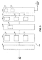
- Figure 3 is a diagram illustrating in greater detail interface circuitry in the integrated circuit of Figure 2.
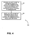
- Figure 4 is a flowchart illustrating operations that may be performed according to an embodiment.
- FIG. 1 illustrates a system embodiment 100 of the claimed subject matter.
- System 100 may include a host processor 12 coupled to a chipset 14.
- Host processor 12 may comprise, for example, an Intel ® Pentium ® IV microprocessor that is commercially available from the Assignee of the subject application.
- host processor 12 may comprise another type of microprocessor, such as, for example, a microprocessor that is manufactured and/or commercially available from a source other than the Assignee of the subject application, without departing from this embodiment.
- Chipset 14 may comprise a host bridge/hub system that may couple host processor 12, a system memory 21 and a user interface system 16 to each other and to a bus system 22.
- Chipset 14 may also include an input/output (I/O) bridge/hub system (not shown) that may couple the host bridge/bus system to bus 22.
- Chipset 14 may comprise integrated circuit chips, such as those selected from integrated circuit chipsets commercially available from the assignee of the subject application (e.g., graphics memory and I/O controller hub chipsets), although other integrated circuit chips may also, or alternatively be used, without departing from this embodiment.
- User interface system 16 may comprise, e.g., a keyboard, pointing device, and display system that may permit a human user to input commands to, and monitor the operation of, system 100.
- Bus 22 may comprise a bus that complies with the Peripheral Component Interconnect (PCI) Express TM Base Specification Revision 1.0, published July 22, 2002, available from the PCI Special Interest Group, Portland, Oregon, U.S.A. (hereinafter referred to as a "PCI Express TM bus”).
- PCI Express TM bus a bus that complies with the PCI-X Specification Rev. 1.Oa, July 24, 2000, available from the aforesaid PCI Special Interest Group, Portland, Oregon, U.S.A.
- PCI-X bus PCI-X bus
- bus 22 may comprise other types and configurations of bus systems, without departing from this embodiment.
- Controller card 20 may be coupled to and control the operation of mass storage 28.
- mass storage 28 may comprise, e.g., one or more redundant arrays of independent disks (RAID) 29.
- RAID level that may be implemented by RAID 29 may be 0, 1, or greater than 1.
- RAID 29 may comprise, for example, one or more disk mass storage devices and/or one or more peripheral devices (collectively or singly shown in Figure 1 by the block referred to by numeral 52) comprised in a protocol domain 50.
- a "protocol domain" means one or more apparatus that may communicate in accordance with a communication protocol.
- Processor 12, system memory 21, chipset 14, bus 22, and circuit card slot 30 may be comprised in a single circuit board, such as, for example, a system motherboard 32.
- Mass storage 28 may be comprised in one or more respective enclosures that may be separate from the enclosure in which the motherboard 32 and the components comprised in the motherboard 32 are enclosed.
- Card 20 may be coupled to mass storage 28 via one or more network communication links 44. As is discussed below, card 20 may exchange data and/or commands with mass storage 28, via links 44, using, e.g., Serial Advanced Technology Attachment (S-ATA) protocol and/or Serial Attached Small Computer Systems Interface (SAS) protocol. Of course, alternatively, I/O controller card 20 may exchange data and/or commands with mass storage 28 using other and/or additional communication protocols, without departing from this embodiment.
- S-ATA Serial Advanced Technology Attachment
- SAS Serial Attached Small Computer Systems Interface
- an S-ATA protocol is used by controller card 20 to exchange data and/or commands with mass storage 28, it may comply or be compatible with the protocol described in "Serial ATA: High Speed Serialized AT Attachment,” Revision 1.0, published on August 29, 2001 by the Serial ATA Working Group.
- SAS Information Technology - Serial Attached SCSI
- IICITS International Committee For Information Technology Standards
- SAS Standard Working Draft American National Standard of International Committee For Information Technology Standards
- circuit card slot 30 may comprise, for example, a PCI Express TM or PCI-X bus compatible or compliant expansion slot or interface 36.
- Interface 36 may comprise a bus connector 37 may be electrically and mechanically mated with a mating bus connector 34 that may be comprised in a bus expansion slot or interface 35 in circuit card 20.
- Circuit card 20 may comprise an integrated circuit 40, operating mode selector circuitry 42, computer-readable boot code memory 39, and computer-readable memory 38.
- integrated circuit 40 may comprise memory 38 and/or memory 39.
- an "integrated circuit” means a semiconductor device and/or microelectronic device, such as, for example, a semiconductor integrated circuit chip.
- Memories 38 and/or 39 each may comprise one or more of the following types of memories: semiconductor firmware memory, programmable memory, non-volatile memory, read only memory, electrically programmable memory, random access memory, flash memory, magnetic disk memory, and/or optical disk memory. Either additionally or alternatively, memories 38 and/or 39 each may comprise other and/or later-developed types of computer-readable memory.
- Machine-readable firmware program instructions may be stored in memory 38. As described below, these instructions may be accessed and executed by integrated circuit 40. When executed by integrated circuit 40, these instructions may result in integrated circuit 40 performing the operations described herein as being performed by integrated circuit 40.
- Slot 30 and card 20 are constructed to permit card 20 to be inserted into slot 30.
- connectors 34 and 36 become electrically and mechanically coupled to each other.
- card 20 becomes electrically coupled to bus 22 and may exchange data and/or commands with system memory 21, host processor 12, and/or user interface system 16 via bus 22 and chipset 14.
- the operative circuitry of card 20 may not be comprised in card 20, but instead, may be comprised in other structures, systems, and/or devices. These other structures, systems, and/or devices may be, for example, comprised in motherboard 32, coupled to bus 22, and exchange data and/or commands with other components (such as, for example, system memory 21, host processor 12, and/or user interface system 16) in system 100.
- FIG. 2 is a diagram of integrated circuit 40.
- integrated circuit 40 may comprise processor circuitry 202, I/O interface circuitry 204, memory control circuitry 232, memory control circuitry 230, processor bus 206, and bus bridge circuitry 208.
- Processor circuitry 202, I/O interface circuitry 204, memory control circuitry 232, memory control circuitry 230, and bus bridge circuitry 208 may be coupled to, and exchange data and/or commands via, bus 206.
- Bus bridge circuitry 208 may couple processor bus 206 to I/O bus 254, and may permit devices that may be coupled to bus 206 to exchange data and/or commands with devices that may be coupled to bus 254, while permitting the respective address spaces of buses 206 and 254 to be isolated from each other.
- Memory control circuitry 230, host bus interface circuitry 210, boot code memory interface 242, and peripheral interface circuitry 244 also may be coupled to bus 254, and may exchange data and/or commands among each other via bus 254.
- Memory control circuitry 230 may be coupled to memory 38.
- Boot code memory interface 242 may be coupled to memory 39.
- Memory control circuitry 232 may be coupled to computer-readable memory 228.
- Memory 228 may comprise, for example, multi-port static random access memory (SRAM), although memory 228 may comprise other types of computer-readable memory without departing from this embodiment.
- Host bus interface circuitry 210 may be coupled host bus interface 35.
- Mode selector circuitry 42 may be coupled to general purpose I/O interface circuitry 248 that may be comprised in interface circuitry 246.
- Interface circuitry 246 may comprise other and/or additional types of interface circuitry (not shown) without departing from this embodiment.
- the interface circuitry comprised in interface 246 may be coupled together via, for example, a peripheral bus (not shown).
- Interface 246 may be coupled to bus 254 via peripheral interface circuitry 244 that may permit the interface circuitry in circuitry 246 that may be coupled to the peripheral bus in circuitry 246 to exchange data and/or commands with devices that may be coupled to bus 254.
- Boot code memory interface circuitry 242 may permit program instructions stored in memory 39 to be retrieved therefrom and executed by processor circuitry 202, after, for example, a reset of integrated circuit 40. More specifically, processor circuitry 202 may provide one or more commands to memory 39 and/or interface circuitry 242, via bus 206, bridge circuitry 208, bus 254, and interface circuitry 242, that may result such program instructions being retrieved from memory 39 and provided to circuitry 202, via interface 242, bus 254, bridge circuitry 208, and bus 206.
- Integrated circuit 40 also may comprise performance monitoring (PMON) circuitry 226.
- PMON circuitry 226 may monitor, e.g., exchange of data and/or commands carried out via bus 206 and/or bus 254, and/or other and/or additional operations carried out by other circuitry in integrated circuit 40, and may determine, based at least in part upon such monitoring, whether integrated circuit 40 is operating properly.
- PMON circuitry 226 may indicate the results of its monitor activities to, e.g., processor circuitry 202 and/or external devices, such as, for example, host processor 12 via circuitry 210.
- Processor circuitry 202 may include processor core circuitry that may comprise a plurality of processor cores 216 and 218.
- processor core may comprise hardwired circuitry, programmable circuitry, and/or state machine circuitry.
- circuitry may comprise, for example, singly or in any combination, hardwired circuitry, programmable circuitry, state machine circuitry, and/or firmware that stores instructions executed by programmable circuitry.
- each processor core 216 and 218 may comprise respective circuitry that may be compatible and/or in compliance with the Intel® XScale TM Core micro-architecture described in "Intel® XScale TM Core Developers Manual,” published December 2000 by the Assignee of the subject application.
- circuitry 202 may comprise other types of processor core circuitry without departing from this embodiment.
- processor cores 216 and 218 may comprise, for example, computer-readable program instruction memory 220 and 224, respectively, that may contain respective sets of micro-code program instructions that processor cores 216 and 218, respectively, may execute.
- the execution of these respective sets of program instructions by processor cores 216 and 218, respectively, may result in, for example, the carrying out by circuitry 202, core 216, and/or core 218 of operations described herein as being carried out by circuitry 202, core 216, and/or core 218, respectively.
- At least a portion of these respective sets of program instructions may be retrieved from, e.g., boot code memory 39 after, for example, a reset of integrated circuit 40.
- Processor core 216 also may comprise a level-2 cache memory 222 that may be used by processor core 216 in carrying out the operations described herein as being carried out by processor core 216.
- Interface circuitry 204 may comprise protocol engine circuitry 250A, 250B, ... 250N and physical layer interface circuitry 252A, 252B, ... 252N.
- each respective protocol engine circuitry 250A, 250B, ... 250N may be associated with, and exchange data and/or commands with respective physical layer interface circuitry 252A, 252B, ... 252N.
- protocol engine circuitry 250A may be associated with, and exchange data and/or commands with physical layer interface circuitry 252A
- protocol engine circuitry 250B may be associated with, and exchange data and/or commands with physical layer interface circuitry 252B
- protocol engine circuitry 250A may be associated with, and exchange data and/or commands with physical layer interface circuitry 252N, respectively.
- each of the protocol engine circuitry 250A, 250B, ...250N may be respectively identical. Additionally, in this embodiment, the respective construction and operation of each of the interfaces 252A, 252B, ... 252N may be respectively identical.
- the respective numbers of protocol engines 252A, 252B, ... 252N, physical layer interfaces 252A, 2S2B, ... 252N, and links 44 may vary.
- the number of protocol engines 250A, 250B, ... 250N may be equal to the number of physical layer interfaces 252A, 252B,... 252N.
- each of the physical layer interfaces 252A, 252B, ... 252N may be coupled to a respective one of the links 44; therefore, in this embodiment, the number of physical layers interfaces 252A, 252B, ... 252N may be equal to the number of links 44.
- Host bus interface circuitry 210 may comprise respective interface circuitry that may be used to permit integrated circuit 40 to be able to exchange, in accordance with one of a plurality of different host bus protocols with which bus 22 may comply or be compatible, data and/or commands with other devices that may be coupled to bus 22.
- circuitry 210 may comprise PCI-X bus interface circuitry 212 and PCI Express TM bus interface circuitry 214.
- a particular operating mode of integrated circuit 40 may be selected in which only a single appropriate one of the respective interface circuitry in circuitry 210 may be enabled to exchange data and/or commands with devices that may be coupled to bus 22, other respective interface circuitry in circuitry 210 may be disabled.
- memory control circuitry 232 and/or DMA circuitry 234 may be coupled to bus 254.
- memory control circuitry 232 may comprise direct memory access (DMA) circuitry 234.
- DMA direct memory access
- Memory control circuitry 232 may control storage of data in, and retrieval of data from memory 228.
- memory control circuitry 232 may exchange commands and/or data with, for example, processor circuitry 202, interface circuitry 204, interface circuitry 210 and/or memory control circuitry 230. Based, at least in part, upon these commands, memory control circuitry 232 may exchange data and/or commands with memory 228.
- DMA circuitry 234 may control, based upon commands and/or data received by circuitry 234 from other circuitry in integrated circuit 40, the exchange among I/O interface 204 and the other circuitry in integrated circuit 40 of data and/or commands received or intended to be transmitted by I/O interface circuitry 204 via one or more links 44.
- DMA circuitry 234 may not be comprised in circuitry 232, but instead, may comprise circuitry that is distinct from circuitry 232, and is coupled to circuitry 232 and bus 254.
- memory control circuitry 230 may comprise RAID operation-related circuitry 240.
- Circuitry 240 may comprise, for example, DMA circuitry 238 and RAID calculation circuitry 236.
- Memory control circuitry 230 may control storage of data in, and retrieval of data from external memory 38.
- memory control circuitry 230 may exchange commands and/or data with, for example, processor circuitry 202, interface circuitry 210 and/or memory control circuitry 232. Based, at least in part, upon these commands, memory control circuitry 230 may exchange data and/or commands with memory 38. This may result in memory 38 storing and/or retrieving data in accordance with the commands and/or data supplied to memory controller circuitry 232.
- DMA circuitry 238 may control, based upon commands and/or data received by circuitry 238 from other circuitry in integrated circuit 40, the exchange of RAID-related data among such other circuitry in integrated circuit 40.
- RAID-related data means data involved in, generated as a result of, used as input or operands in, and/or used in carrying out and/or to facilitate operations involved in implementing and/or maintaining a RAID, such as, for example, RAID 29.
- RAID calculation circuitry 236 may comprise arithmetic accelerator circuitry (not shown) that may be capable of performing one or more arithmetic and/or logical operations using and/or involving RAID-related data, such as, for example, logical exclusive-or operations that may generate RAID parity data from initial user data and/or regenerate the initial user data from such RAID parity data.
- DMA circuitry 238 and/or RAID calculation circuitry 236 may not be comprised in circuitry 230, but instead, may comprise circuitry that is distinct from circuitry 230, and is coupled to circuitry 230 and bus 254.
- integrated circuit 40 may not comprise RAID calculation circuitry 236, but alternatively, the arithmetic and/or logical operations performed by circuitry 236 instead may be performed by processor core 216.
- Protocol engine 250A may comprise interface circuitry 302, data transport layer circuitry 304, port layer circuitry 306, data link layer circuitry 308, and SAS link layer circuitry 310.
- circuitry 302 may couple circuitry 304, 306, 308, and 310 to bus 206 so as to permit circuitry 304, 306, 308, and/or 310 to exchange data and/or commands with processor core 218.
- SAS link layer circuitry 310 may be coupled to, and exchange data and/or commands with physical interface circuitry 252A.
- Transport layer circuitry 304 may be coupled to, and exchange data and/or commands with port layer circuitry 306.
- Port layer circuitry 306 also may be coupled to, and exchange data and/or commands with data link layer circuitry 308.
- SAS link layer circuitry 310 may be coupled to, and exchange data and/or commands with data link layer circuitry 308 and port layer circuitry 306.
- transport layer circuitry 304 may comprise Serial Management Protocol (SMP) transport layer circuitry 312, Serial Advanced Technology Attachment (ATA) Tunneled Protocol (STP) transport layer circuitry 314, and Serial Small Computer System Interface (SCSI) Protocol (SSP) transport layer circuitry 316.
- port layer circuitry 306 may comprise connection management circuitry 318.
- data link layer circuitry 308 may comprise SMP link layer circuitry 320, STP link layer circuitry 322, and SSP link layer 324 circuitry.
- SAS link layer circuitry 310 may comprise out-of-band (OOB) signal management circuitry 326 and S-ATA link speed negotiation control circuitry 328.
- OOB out-of-band
- circuitry 304, 306, 308, and 310 may implement conventional SAS communication processes, procedures, and techniques.
- circuitry 312, 314, and 316 may implement conventional SMP transport layer, STP transport layer, and SSP transport layer protocols, procedures, processes, and techniques, respectively, and also may generate respective sets of signals that may result in the carrying out of such protocols, procedures, processes, and techniques.
- circuitry 306 may implement conventional SAS port control protocols, procedures, processes, and techniques, and also may generate respective signals that may result in the carrying out of such protocols, procedures, processes, and techniques.
- circuitry 320, 322, and 324 may implement conventional SMP link layer, STP link layer, and SSP link layer protocols, procedures, processes, and techniques, respectively, and also may generate respective sets of signals that may result in the carrying out of such protocols, procedures, processes, and techniques.
- circuitry 310 may implement conventional SAS data link protocols, procedures, processes, and techniques to control, e.g., physical interface 252A, and also may generate respective sets of signals that may result in the carrying out of such protocols, procedures, processes, and techniques.
- many variations, modifications, and alternatives are possible without departing from this embodiment.
- each physical layer interface circuitry 252A, 252B, ... 252N may comprise respective analog front end (AFE) circuitry 253A, 253B, ... 253N that may receive and/or transmit data and/or control signals to and/or from mass storage 28 via respective links 44.
- AFE analog front end
- physical layer interface circuitry 252A may comprise AFE circuitry 253A that may receive and/or transmit data and/or control signals to and/or from one or more external mass storage devices comprised in one or more devices 52 via one of the links 44.
- protocol domain 50 may be either an SAS domain or an S-ATA domain. If protocol domain 50 is an SAS domain, then one or more devices 52 may be capable of communicating using an SAS protocol via one of the links 44. Conversely, if protocol domain 50 is an S-ATA domain, then one or more devices 52 may be capable of communicating using an S-ATA protocol via one of the links 44.
- integrated circuit 40 may be capable of discovering, at least in part, whether one or more devices 52 are capable of communicating via an SAS communication protocol or via an S-ATA communication protocol. Based upon this discovery, at least in part, by integrated circuit 40, integrated circuit 40 may select, at least in part, whether to communicate with one or more devices 52 using either an SAS or an S-ATA communication protocol, in order to enable integrated circuit 40 to communicate with one or more devices 52.
- OOB signal sequences may be exchanged between AFE circuitry 253A and one or more mass devices 52 via one of the links 44.
- one or more devices 52 may be expected to transmit to AFE circuitry 253A during an S-ATA OOB signal sequence predetermined, special primitive signal sequence (referred to in Figure 1 by the block referenced by numeral 54) that may comprise, e.g., a predetermined comma character, such as, a K28.5 character.
- a "signal sequence" comprises one or more signals.
- one or more devices 52 may be expected not to transmit to AFE circuitry 253A this predetermined, special signal sequence 54 during an SAS OOB signal sequence, but instead may be expected to transmit to AFE circuitry 253A during this signal sequence a predetermined COMSAS signal sequence 56.
- AFE circuitry 253A receives from one or more devices 52 signal sequence 54, but does not receive COMSAS signal sequence 56, this may indicate that protocol domain 50 is an S-ATA domain, one or more devices 52 are directly coupled to AFE circuitry 253A via one of the links 44, and one or more devices 52 are capable of communicating with integrated circuit 40 via an S-ATA protocol. Conversely, if, during such an OOB signal sequence, AFE circuitry 253A receives from one or more devices 52 COMSAS signal sequence 56, but does not receive signal sequence 54, this may indicate that protocol domain 50 is an SAS domain and one or more devices 52 are capable of communicating with integrated circuit via an SAS protocol.
- physical interface circuitry 252A may provide to OOB management circuitry 320 signals indicative of OOB signals received by AFE circuitry 253A from one or more devices 52.
- OOB management circuitry 320 may examine the signals provided to it from interface circuitry 252A to detect whether AFE circuitry 253A has received, during an OOB signal sequence, from one or more devices 52, signal sequence 54 or COMSAS signal sequence 56.
- OOB management circuitry 320 may provide one or more signals to processor core 218 that may indicate whether AFE circuitry 253A has received signal sequence 54 or COMSAS signal sequence 56.
- processor core 218 may determine, based at least in part upon whether OOB management circuitry 320 detected that AFE circuitry 253A received, or failed to receive, during the OOB signal sequence, signal sequence 54 and/or COMSAS signal sequence 56, whether one or more devices 52 are directly coupled to integrated circuit 40 via one of the links 44 and are capable of communicating with integrated circuit 40 via an S-ATA protocol, or one or more devices 52 are capable of communicating with integrated circuit 40 via an SAS protocol.
- processor core 218 may determine that one or more devices 52 are directly coupled to AFE circuitry 253A via one of the links 44 and are capable of communicating with integrated circuit 40 via an S-ATA protocol. Conversely, if circuitry 320 detected that AFE circuitry 253A received, during this OOB signal sequence, from one or more devices 52 COMSAS signal sequence 56, but did not receive signal sequence 54, processor core 218 may determine that one or more devices 52 are capable of communicating with integrated circuit 40 via an SAS protocol.
- character 54 and/or signal 56 may vary without departing from this embodiment.
- the manner in which integrated circuit 40 may determine the communication protocol or protocols via which one or more devices 52 may be capable of communicating may vary without departing from this embodiment.
- processor core 218 may issue one or more respective signals to circuitry 304, 306, 308, 310, and 252A. This may result in circuitry 250A and 252A being enabled to permit integrated circuit 40 to communicate directly with one or more devices 52, using S-ATA protocol, via one of the links 44.
- circuitry 312, 316, 318, 320, and 324 may result in, for example, the disabling of circuitry 312, 316, 318, 320, and 324 from being involved in communications between integrated circuit 40 and one or more devices 52, and may also result in the enabling of circuitry 314, 322, and 328 to be actively involved in carrying out communications between integrated circuit 40 and one or more devices 52.
- circuitry 310 may signal circuitry 306 and/or circuitry 318; this may result in the disabling of circuitry 318 from being involved in communications between integrated circuit 40 and one or more devices 52.
- the signaling of circuitry 252A by processor core 218 may result, at least in part, in the transmission and/or reception signaling levels of AFE circuitry 253A being set so as to be in compliance or compatible with S-ATA signal transmission and/or reception signaling levels. That is, this may result in AFE circuitry 253A adjusting the voltage and/or current levels of signals transmitted to one or more devices 52 by AFE circuitry 253A to be in compliance or compatible with S-ATA transmission signal voltage and/or current levels, and/or may also result in AFE circuitry 253A detecting signals received by AFE circuitry 253A whose voltage and/or current levels are in compliance or compatible with S-ATA received signal voltage and/or current levels.
- circuitry 310 may result in the enabling of circuitry 328 to implement conventional S-ATA communication link speed negotiation protocols, procedures, processes, and techniques to negotiate with one or more devices 52 the appropriate speed of communication to be carried out, via one of the links 44, between one or more devices 52 and integrated circuit 40.
- Circuitry 310 may generate and transmit to interface 252A one or more signals that may result in the carrying out of such protocols, procedures, processes, and techniques.
- circuitry 318 when circuitry 318 is enabled to be actively involved in carrying out communications between integrated circuit 40 and one or more devices 52, circuitry 318 may implement, at least in part, connection management functions that may prevent, at least in part, timing-out of the communications between integrated circuit 40 and one or more devices 52. Conversely, in operation of system 100, when circuitry 318 is disabled from being actively involved in carrying out such communications, processor core 218 may provide one or more signals to circuitry 250A that may result in circuitry 250A emulating S-ATA host functionality that may result in the maintaining, without timing-out, of such communications.
- processor core 218 may issue one or more respective signals to circuitry 304, 306, 308, 310, and 252A. This may result in circuitry 250A and 252A being enabled to permit integrated circuit 40 to communicate with one or more devices 52, using an SAS protocol, via one of the links 44. More specifically, the signaling of circuitry 304, circuitry 306, and circuitry 308 may result in the disabling of circuitry 314 from being actively involved in communications between integrated circuit 40 and one or more devices 52, the enabling of circuitry 318 to be actively involved in such communications, and the disabling of circuitry 322 from being involved in such communications, respectively.
- the signaling of circuitry 304 by processor core 218 may result in the enabling of circuitry 312 or 316, respectively, to be actively involved in such communications, and the signaling of circuitry 308 by processor core 218 may result in the enabling of circuitry 320 or 324, respectively, to be involved in such communications. Additionally, the signaling of circuitry 252A by processor core 218 may result, at least in part, in the transmission and/or reception signaling levels of AFE circuitry 253A being set so as to be in compliance or compatible with SAS signal transmission and/or reception signaling levels.
- AFE circuitry 253A may result in AFE circuitry 253A adjusting the voltage and/or current levels of signals transmitted to one or more devices 52 by AFE circuitry 253A to be in compliance or compatible with SAS transmission signal voltage and/or current levels, and/or may also result in AFE circuitry 253A detecting signals received by AFE circuitry 253A whose voltage and/or current levels are in compliance or compatible with SAS received signal voltage and/or current levels.
- the signaling of circuitry 310 by processor core 218 may result in the disabling of circuitry 328 from implementing conventional S-ATA communication link speed negotiation protocols, procedures, processes, and techniques described previously.
- a mode of operation of integrated circuit 40 may be selected, based upon and/or as a result of, at least in part, of one or more signals provided to GPIO interface circuitry 248 from selector circuitry 42, one or more signals provided to host bus interface circuitry 210 by host processor 12, and/or execution by processor circuitry 202 of one or more program instructions stored in memory 39.
- integrated circuit 40 may operate in accordance with one or more operational characteristics that may correspond to the selected mode of operation.
- these operational characteristics may include which of bus interfaces 212 and 214 is enabled to or disabled from communicating with bus 22, and/or which protocol engines 250A, 250B, ... 250N are enabled to or disabled from communicating with mass storage 28. Additionally or alternatively, such operational characteristics may comprise, for example, whether one or more of the communication protocols that are implemented by one or more of the protocol engines 250A, 250B, ... 250N are selected based at least in part upon the discovery of one or more communication protocols via which one or more devices (such as, for example, one or more devices 52) in mass storage 28 may communicate, or whether communication between integrated circuit and such devices is to be carried out via one or more predetermined protocols.
- one or more devices such as, for example, one or more devices 52
- Such operational characteristics may comprise whether DMA circuitry 234 is enabled to control or disabled from controlling the exchange among I/O interface 204 and the other circuitry in integrated circuit 40 of data and/or commands received or intended to be transmitted by I/O interface circuitry 204 via one or more links 44.
- Such operational characteristics may also include, for example, whether processor core 216 and/or RAID operation-related circuitry 240 are enable to perform or disabled from performing one or more operations involved in implementing and/or maintaining a RAID, such as, for example, RAID 29. Examples of such operations that may be involved in implementing and/or maintain a RAID are disclosed in, e.g., co-pending U.S. Patent Application Serial No. 10/301,028 (Attorney Docket No. 42390.P14962), entitled "Integrated Circuit Having Multiple Modes Of Operation," filed on November 20, 2002.
- U.S. Patent Application Serial No. 10/301,028 (Attorney Docket No. 42390.P14962), entitled "Integrated
- selector circuitry 42 may comprise one or more jumpers and/or one or more dual in-line package (DIP) switches 43 that may be set (e.g., by a not shown human operator) in a plurality of different configurations to select, at least in part, the selected operating mode of integrated circuit 40. That is, the plurality of different configurations of the jumper and/or switches 43 may correspond to one or more different operating characteristics of one or more different operating modes of integrated circuit 40.
- the selector circuitry 42 may generate one or more control signals that may correspond to one or more different operating characteristics of integrated circuit 40 selected by that particular configuration.
- these one or more control signals may be supplied to processor cores 216 and 218.
- processor core 216 may be enabled or disabled in accordance with the selected mode of operation; additionally, processor core 218 may operate in accordance with and/or generate and supply appropriate control signals to interface circuitry 204, 210, 232, and/or 236 that may result in such circuitry operating in accordance with the selected mode of operation.
- the one or more control signals from selector circuitry 42 also may be supplied to circuitry 210, circuitry 234, and/or circuitry 240.
- bus interface circuitry 212 bus interface circuitry 214, circuitry 240, and/or circuitry 234 in accordance with the mode of operation of integrated circuit 40 that corresponds to and/or is indicated by the one or more control signals.
- the selected mode of operation of integrated circuit 40 may be selected based upon and/or as a result, at least in part, of one or more signals indicative of the selected mode of operation that may be provided to host bus interface circuitry 210 by host processor 12.
- processor core 216 may be enabled or disabled in accordance with the selected mode of operation; additionally, processor core 218 may operate in accordance with and/or generate and supply appropriate control signals to interface circuitry 204, 210, 232, and/or 236 that may result in such circuitry operating in accordance with the selected mode of operation.
- the selected mode of operation of integrated circuit 40 may be selected based upon and/or as a result, at least in part, of execution by processor circuitry 202 of one or more program instructions stored in memory 39, memory 220, and/or memory 224. That is, according to this embodiment, different respective operating modes of integrated circuit 40 may be associated with different respective firmware program instruction set images that when executed, at least in part, by processor core 216 and processor core 218 may result in the respective operating modes being associated with these respective images being selected, and also may result in integrated circuit 40 operating in the respective operating modes. In this embodiment, only a single such firmware program instruction set image may be stored in memory 39, memory 220, and/or memory 224.
- This single firmware program instruction set image may comprise one or more firmware program instructions that may be executed by processor cores 216 and processor 218 after, for example, a reset of integrated circuit 40. This may result in processor core 216 being enabled or disabled in accordance with the selected mode of operation. This may also result in processor core 218 operating in accordance with and/or generating and supplying appropriate control signals to interface circuitry 204, 210, 232, and/or 236 that may result in such circuitry operating in accordance with the selected mode of operation.
- Memory 39, memory 220, and/or memory 224 may comprise program instructions that, when executed by integrated circuit 40, may result in, among other things, integrated circuit 40 performing operations in accordance with one embodiment.
- Figure 4 is a flowchart that illustrates these and other operations 400 that may be carried out in system 100, in accordance with one embodiment.
- operations 400 may be carried out in system 100 after an operating mode of integrated circuit 40 has been selected in which one or more of the communication protocols that are implemented by one or more of the protocol engines 250A, 250B, ... 250N (e.g., protocol engine 250A) are selected based at least in part upon the discovery of one or more communication protocols via which one or more devices (such as, for example, one or more devices 52) in mass storage 28 may communicate.
- Operations 400 may commence with the discovery, at least in part, by integrated circuit 40, of at least one communication protocol via which at least one device external to integrated circuit 40 (e.g., one or more devices 52) may be capable of communicating, as illustrated by operation 402 in Figure 4.
- the discovery at least in part, by integrated circuit 40 of the at least one communication protocol via which at least one device external to integrated circuit 40 may communicate, as a result of operation 402, may be based; at least in part, upon a determination by processor core 218, in the manner described previously, of whether OOB management circuitry 320 detected that AFE circuitry 253A received, or failed to receive, during the OOB signal sequence, signal sequence 54 and/or COMSAS signal sequence 56.
- processor core 218 may determine that one or more devices 52 are directly coupled to AFE circuitry 253A via one of the links 44 and are capable of communicating with integrated circuit 40 via an S-ATA protocol; as a result, at least in part, of this determination by processor core 218, integrated circuit may discovery at least in part, as a result of operation 402, that one or more devices 52 are capable of communicating via an S-ATA protocol.
- processor core 218 may determine that one or more devices 52 are capable of communicating with integrated circuit 40 via an SAS protocol; as a result, at least in part, of this determination by processor core 218, integrated circuit may discovery at least in part, as a result of operation 402, that one or more devices 52 are capable of communicating via an SAS protocol.
- integrated circuit 40 may select, at least in part, the at least one communication protocol to use to communicate with the at least one device, as illustrated by operation 404 in Figure 4. For example, in this embodiment, after discovering, as a result of operation 402, the at least one protocol via which one or more devices 52 may communicate, processor core 218 may issue one or more respective signals to circuitry 304, 306, 308, 310, and 252A. If, as a result of operation 402, integrated circuit 40 discovered that one or more devices 52 may be capable of communicating via an S-ATA protocol, this may result in circuitry 250A and 252A being enabled to permit integrated circuit 40 to communicate directly with one or more devices 52 using an S-ATA protocol, via one of the links 44.
- circuit 40 discovered that one or more devices 52 may be capable of communicating via an SAS protocol, this may result in circuitry 250A and 252A being enabled to permit integrated circuit 40 to communicate with one or more devices 52 using an SAS protocol.
- one system embodiment may comprise a circuit card including an integrated circuit.
- the circuit card may be capable of being coupled to a bus.
- the integrated circuit may be capable of discovering, at least in part, at least one communication protocol via which at least one device external to the integrated circuit is capable of communicating.
- the integrated circuit also may be capable of communicating in accordance with a plurality of different communication protocols.
- the integrated circuit further may be capable of selecting, at least in part, the at least one communication protocol to use to communicate with the at least one device.
- One apparatus embodiment may include an integrated circuit that is capable of discovering, at least in part, at least one communication protocol via which at least one device external to the integrated circuit is capable of communicating.
- the integrated circuit also may be capable of communicating in accordance with a plurality of different communication protocols.
- the integrated circuit further may be capable of selecting, at least in part, the at least one communication protocol to use to communicate with the at least one device.
- the integrated circuit of these embodiments may offer enhanced communication capabilities, and may communicate using a plurality of communication protocols.
- the communication protocol or protocols used by this integrated circuit may be selected, at least in part by the integrated circuit, based at least in part, upon the discovery by the integrated circuit, at least in part, of the one or more communication protocols via which one or more external devices are capable of communicating. Further advantageously, this may permit a single integrated circuit according to these embodiments to communicate with a data storage system directly using a plurality of different communication protocols.
- the integrated circuit of these embodiments may be used to communicate directly via one or more communication links with one or more devices in SAS and/or S-ATA protocol domains in the data storage system, without having to employ one or more external communication protocol converters, translators, and/or expanders (such as, for example, one or more SAS expanders) coupled between the integrated circuit and the data storage system, although such protocol converters, translators, and/or expanders may be used without departing from these embodiments.
- these features may permit the integrated circuit of these embodiments to exhibit enhanced versatility and utility compared to the prior art, and may reduce design costs of employing this integrated circuit compared to the
- circuitry 302 and the circuitry in integrated circuit 40 that is external to circuitry 250A may together be viewed, at least in part, in conceptual, behavioral, and/or functional sense, as comprising, at least in part, a single control element to control which communication protocol may be used by the integrated circuit 40 to communicate with the at least one device.
- this control element may comprise, for example, singly or in any combination, hardwired circuitry, programmable circuitry, state machine circuitry, and/or firmware that stores instructions executed by programmable circuitry.
- system 100 may include more or fewer than the elements shown in the Figures and described previously herein as being comprised system 100.
- circuitry 204 may comprise protocol engine circuitry that may permit integrated circuit 40 to be able to communicate with mass storage 28 using a Fibre Channel protocol that complies or is compatible with the interface/protocol described in ANSI Standard Fibre Channel (FC) Physical and Signaling Interface-3 X3.303:1998 Specification.
- FC Fibre Channel
Landscapes
- Engineering & Computer Science (AREA)
- Theoretical Computer Science (AREA)
- Physics & Mathematics (AREA)
- General Engineering & Computer Science (AREA)
- General Physics & Mathematics (AREA)
- Bus Control (AREA)
- Communication Control (AREA)
- Semiconductor Integrated Circuits (AREA)
- Polysaccharides And Polysaccharide Derivatives (AREA)
- Optical Communication System (AREA)
- Networks Using Active Elements (AREA)
Claims (18)
- Verfahren, umfassend:Auswählen einen von mehreren Betriebsmodi eines einzelnen integrierten Schaltkreises (40), der zwischen einem Hostbus (22) und einem Satz eines oder mehrerer Speichervorrichtungen (29) gekoppelt ist; undauf Grundlage des ausgewählten Betriebsmodus, Aktivieren mindestens eines der folgenden:eines von mehreren Speicherprotokollen zum Kommunizieren mit dem Satz einer oder mehrerer Speichervorrichtungen, undeines oder mehrerer Vorgänge zum Verwalten eines RAID-(Redundant Array of Independent Disks) Systems (29), das den Satz einer oder mehrerer Speichervorrichtungen aufweist.
- Verfahren nach Anspruch 1, ferner umfassend:Aktivieren oder Deaktivieren eines von mehreren Hostbusprotokollen auf Grundlage des ausgewählten Betriebsmodus.
- Verfahren nach Anspruch 1, ferner umfassend:Aktivieren oder Deaktivieren eines DMA- (Direct Memory Access) Vorgangs auf Grundlage des ausgewählten Betriebsmodus, wobei der DMA-Vorgang das Steuern eines Austauschs von Befehlen und Daten aufweist.
- Verfahren nach Anspruch 1, wobei das Auswählen Folgendes umfasst:Speichern eines oder mehrerer Programmbefehle, wobei der eine oder die mehreren Programmbefehle mit einem der mehreren Betriebsmodi verbunden sind;Ausführen des einen oder der mehreren Programmbefehle.
- Verfahren nach Anspruch 1, wobei das Auswählen Folgendes umfasst:Erkennen eines oder mehrerer Speicherprotokolle, die von dem Satz von Speichervorrichtungen benutzt werden.
- Verfahren nach Anspruch 1, wobei das Auswählen Folgendes umfasst:Lesen einer Eingabevorrichtung (43), um zu erkennen, welche von mehreren unterschiedlichen Konfigurationen ausgewählt wird, wobei jede der mehreren Konfigurationen einem der mehreren Betriebsmodi des einzelnen integrierten Schaltkreises (40) entspricht.
- Computerlesbares Speichermedium mit darauf gespeicherten Befehlen, die bei Ausführung von einer Maschine dazu führen, dass die Maschine dazu fähig ist, die Verfahrensschritte nach einem der Ansprüche 1 bis 6 auszuführen.
- Vorrichtung, umfassend:einen einzelnen integrierten Schaltkreis (40), der zwischen einem Hostbus und einem Satz eines oder mehrerer Speichervorrichtungen (29) gekoppelt ist und für mehrere Betriebsmodi konfiguriert werden kann, wobei der einzelne integrierte Schaltkreis (40) Folgendes aufweist:eine Prozessorschaltung (202), die mit einer internen Busschaltung (206, 254) gekoppelt und konfiguriert ist, um ein oder mehrere Steuersignale zu erzeugen, die einem ausgewählten der mehreren Betriebsmodi des integrierten Schaltkreises (40) entsprechen,eine Hostbus-Schnittstellenschaltung (210), die mit dem Hostbus (22) gekoppelt ist und mit der internen Busschaltung (206, 254) gekoppelt und konfiguriert ist, um das eine oder die mehreren Steuersignale über die interne Busschaltung (206, 254) zu empfangen, wobei die Hostbus-Schnittstellenschaltung (206, 254) mittels mehrerer Hostbusprotokolle kommunizieren kann und konfiguriert ist, um in Abhängigkeit des ausgewählten der mehreren Betriebsmodi mittels eines der mehreren Hostbusprotokolle zu kommunizieren,eine Eingabe-/Ausgabe- (I/O) Schnittstellenschaltung (204), die mit dem Satz von Speichervorrichtungen (29) gekoppelt ist und mit der internen Busschaltung (206, 254) gekoppelt und konfiguriert ist, um das eine oder die mehreren Steuersignale über die interne Busschaltung (206, 254) zu empfangen, wobei die I/O-Schnittstellenschaltung (204) mittels mehrerer Speicherprotokolle kommunizieren kann und konfiguriert ist, um in Abhängigkeit des ausgewählten der mehreren Betriebsmodi mittels eines der mehreren Speicherprotokolle zu kommunizieren, undeine RAID-vorgangsbezogene Schaltung (240), die mit der internen Busschaltung (206, 254) gekoppelt und konfiguriert ist, um das eine oder die mehreren Steuersignale von der Prozessorschaltung (202) zu empfangen, und die zum Ausführen einer der mehreren Vorgänge, die an der Ausführung eines RAID beteiligt sind, in Abhängigkeit von dem ausgewählten der mehreren Betriebsmodi aktiviert oder zum Nichtausführen davon deaktiviert wird.
- Vorrichtung nach Anspruch 8, wobei:die Prozessorschaltung (202) einen ersten Prozessorkern (216) und einen zweiten Prozessorkern (214) aufweist, wobei der erste Prozessorkern (216) ein erste Steuersignal an die Hostbus-Schnittstellenschaltung (210) und ein zweites Steuersignal an die I/O-Schnittstellenschaltung liefert und der zweite Prozessorkern (214) ein drittes Steuersignal an die RAID-vorgangsbezogene Schaltung (240) liefert.
- Vorrichtung nach Anspruch 8, wobei:die Hostbusschaltung (210) eine erste Schaltung (214) und eine zweite Schaltung (212) aufweist;die erste Schaltung (214) die Kommunikation über den Hostbus mittels PCI- (Peripheral Component Interconnect) Express herstellt;die zweite Schaltung (212) die Kommunikation über den Hostbus mittels PCI-X herstellt.
- Vorrichtung nach Anspruch 8, wobei:die I/O-Schnittstellenschaltung (204) mehrere Protokollmotoren (250A, 250B, ..., 250N) und eine entsprechende Schnittstellenschaltung für die physikalische Schicht (252A, 252B,..., 250N) aufweist, um jedes der mehreren Speicherprotokolle umzusetzen, wobei jeder Protokollmotor (250A, 250B, ..., 250N) über die entsprechende Schaltung für die physikalische Schicht (252A, 252B,..., 252N) gemäß den mehreren unterschiedlichen Protokollen kommunizieren kann.
- Vorrichtung nach Anspruch 8, wobei:die mehreren Speicherprotokolle SAS (Serial Small Computer Interface); SATA (Serial Advanced Technology Attachment) und/oder FC (Fibre Channel) aufweisen.
- Vorrichtung nach Anspruch 8, wobei der einzelne integrierte Schaltkreis (40) ferner Folgendes umfasst:eine GPIO- (General Purpose Input Output) Schnittstelle (248), die zum Empfangen eines Steuersignals, das außerhalb des einzelnen integrierten Schaltkreises (40) erzeugt wird, konfiguriert ist; undeine periphere Schnittstellenschaltung (246), um die GPIO-Schnittstelle (248) mit der internen Busschaltung (206, 254) kommunikativ zu koppeln;wobei die Prozessorschaltung (202) konfiguriert ist, um das eine oder die mehreren Steuersignale in Antwort auf das Steuersignal, das über die GPIO-Schnittstelle (248) empfangen wird, zu erzeugen.
- Vorrichtung nach Anspruch 13, ferner umfassend:eine externe Wählerschaltung (42), die mit dem integrierten Schaltkreis (40) über die GPIO-Schnittstelle (248) gekoppelt ist, wobei das Steuersignal auf einer physikalischen Konfiguration mindestens entweder einer Drahtbrücke oder eines DIP- (dual in-line package) Schalters (43) beruht.
- Vorrichtung nach Anspruch 8, wobei:der integrierte Schaltkreis (40) einen Speicher (39, 220, 224) aufweist, um einen oder mehrere Programmbefehle zu speichern, wobei der eine oder die mehreren Programmbefehle zum Bestimmen des ausgewählten der mehreren Betriebsmodi des integrierten Schaltkreises (40) benutzt werden; unddie Prozessorschaltung (202) konfiguriert ist, um auf den Speicher (39, 220, 224) über die interne Busschaltung (206, 254) zuzugreifen, um den einen oder die mehreren Programmbefehle zu bestimmen und das eine oder die mehreren Steuersignale auf Grundlage des einen oder der mehreren Programmbefehle zu erzeugen.
- Vorrichtung nach Anspruch 15, wobei:der eine oder die mehreren Programmbefehle, die in dem Speicher (39, 220, 224) gespeichert sind, einen Programmbefehlssatz aufweisen, der mit einem der mehreren Betriebsmodi in Verbindung steht; unddie Prozessorschaltung (202) konfiguriert ist, um den Programmbefehlssatz, der in dem Speicher (39, 220, 224) gespeichert ist, auszuführen und das eine oder die mehreren Steuersignale auf Grundlage der Ausführung zu erzeugen.
- Vorrichtung nach Anspruch 8, wobei:die I/O-Schnittstellenschaltung (204) konfiguriert ist, um jedes der mehreren Speicherprotokolle zu erkennen, die von dem Satz eines oder mehrerer Speichervorrichtungen empfangen werden, mit denen die I/O-Schnittstellenschaltung (204) kommunizieren kann, und um der Prozessorschaltung (202) ein erkanntes Speicherprotokoll anzuzeigen; unddie Prozessorschaltung (202) konfiguriert ist, um die Anzeige über die interne Busschaltung (206, 254) zu empfangen und das eine oder die mehreren Steuersignale auf Grundlage des erkannten Speicherprotokolls zu erzeugen.
- System, umfassend:Kopplungsmittel zum Koppeln eines einzelnen integrierten Schaltkreises (40) mit einem Satz einer oder mehrerer Speichervorrichtungen (29), wobei das Kopplungsmittel eine Verknüpfung umfasst, die konfiguriert ist, um die Kommunikation zwischen SAS- und SATA-Vorrichtungen herzustellen; undder einzelne integrierte Schaltkreis (40) einen einzelnen integrierten Schaltkreis (40) gemäß der Vorrichtung nach einem der Ansprüche 8 bis 17 umfasst.
Applications Claiming Priority (2)
| Application Number | Priority Date | Filing Date | Title |
|---|---|---|---|
| US10/442,705 US7093033B2 (en) | 2003-05-20 | 2003-05-20 | Integrated circuit capable of communicating using different communication protocols |
| PCT/US2004/012021 WO2004104844A2 (en) | 2003-05-20 | 2004-04-16 | Integrated circuit capable of communicating using different communication protocols |
Publications (2)
| Publication Number | Publication Date |
|---|---|
| EP1636705A2 EP1636705A2 (de) | 2006-03-22 |
| EP1636705B1 true EP1636705B1 (de) | 2007-08-01 |
Family
ID=33476625
Family Applications (1)
| Application Number | Title | Priority Date | Filing Date |
|---|---|---|---|
| EP04785488A Expired - Lifetime EP1636705B1 (de) | 2003-05-20 | 2004-04-16 | Integrierter schaltkreis, der mithilfe verschiedener kommunikationsprotokolle kommunizieren kann |
Country Status (7)
| Country | Link |
|---|---|
| US (1) | US7093033B2 (de) |
| EP (1) | EP1636705B1 (de) |
| CN (1) | CN100412835C (de) |
| AT (1) | ATE368893T1 (de) |
| DE (1) | DE602004007927T2 (de) |
| TW (1) | TWI281612B (de) |
| WO (1) | WO2004104844A2 (de) |
Cited By (1)
| Publication number | Priority date | Publication date | Assignee | Title |
|---|---|---|---|---|
| CN101359309B (zh) * | 2007-08-03 | 2012-03-07 | 中兴通讯股份有限公司 | 串行附接小型计算机系统接口硬盘状态指示装置及方法 |
Families Citing this family (45)
| Publication number | Priority date | Publication date | Assignee | Title |
|---|---|---|---|---|
| US7058703B2 (en) * | 2002-03-08 | 2006-06-06 | Intel Corporation | System management controller (SMC) negotiation protocol for determining the operational mode of SMCs |
| US7206989B2 (en) * | 2002-11-20 | 2007-04-17 | Intel Corporation | Integrated circuit having multiple modes of operation |
| US7543085B2 (en) * | 2002-11-20 | 2009-06-02 | Intel Corporation | Integrated circuit having multiple modes of operation |
| US7093033B2 (en) * | 2003-05-20 | 2006-08-15 | Intel Corporation | Integrated circuit capable of communicating using different communication protocols |
| US20050015655A1 (en) * | 2003-06-30 | 2005-01-20 | Clayton Michele M. | Intermediate station |
| US8539096B2 (en) * | 2003-09-26 | 2013-09-17 | Lsi Corporation | Systems and methods for configuring ports of an SAS domain |
| US20050138154A1 (en) * | 2003-12-18 | 2005-06-23 | Intel Corporation | Enclosure management device |
| US7376147B2 (en) * | 2003-12-18 | 2008-05-20 | Intel Corporation | Adaptor supporting different protocols |
| US7155546B2 (en) * | 2003-12-18 | 2006-12-26 | Intel Corporation | Multiple physical interfaces in a slot of a storage enclosure to support different storage interconnect architectures |
| US7353302B2 (en) * | 2003-12-31 | 2008-04-01 | Intel Corporation | Selectable communication control between devices communicating using a serial attached SCSI (SAS) protocol |
| US7363395B2 (en) * | 2003-12-31 | 2008-04-22 | Intel Corporation | Intermediate device capable of communicating using different communication protocols |
| US7418646B2 (en) * | 2004-03-02 | 2008-08-26 | Intel Corporation | Integrated circuit using wireless communication to store and/or retrieve data and/or check data |
| FR2875026A1 (fr) * | 2004-09-03 | 2006-03-10 | St Microelectronics Sa | Dispositif programmable d'interface de commande |
| US7949806B2 (en) * | 2004-11-18 | 2011-05-24 | International Business Machines Corporation | Apparatus and method to provide an operation to an information storage device including protocol conversion and assigning priority levels to the operation |
| US7805543B2 (en) * | 2005-06-30 | 2010-09-28 | Intel Corporation | Hardware oriented host-side native command queuing tag management |
| US7970953B2 (en) * | 2005-06-30 | 2011-06-28 | Intel Corporation | Serial ATA port addressing |
| US7747788B2 (en) * | 2005-06-30 | 2010-06-29 | Intel Corporation | Hardware oriented target-side native command queuing tag management |
| US20070011333A1 (en) | 2005-06-30 | 2007-01-11 | Victor Lau | Automated serial protocol initiator port transport layer retry mechanism |
| US20070005833A1 (en) * | 2005-06-30 | 2007-01-04 | Pak-Lung Seto | Transmit buffers in connection-oriented interface |
| US8135869B2 (en) * | 2005-06-30 | 2012-03-13 | Intel Corporation | Task scheduling to devices with same connection address |
| US7734839B1 (en) * | 2005-08-25 | 2010-06-08 | American Megatrends, Inc. | Method and integrated circuit for providing enclosure management services utilizing multiple interfaces and protocols |
| US7525957B2 (en) * | 2005-09-01 | 2009-04-28 | Emulex Design & Manufacturing Corporation | Input/output router for storage networks |
| US7676604B2 (en) * | 2005-11-22 | 2010-03-09 | Intel Corporation | Task context direct indexing in a protocol engine |
| US7752343B2 (en) * | 2006-02-22 | 2010-07-06 | Emulex Design & Manufacturing Corporation | Method and apparatus for auto-protocol discrimination between fibre channel, SAS and SATA devices |
| US7529877B2 (en) * | 2006-03-13 | 2009-05-05 | Lsi Corporation | Apparatus and methods for simplified SSP link layer processing |
| US20080074285A1 (en) * | 2006-08-31 | 2008-03-27 | Guthrie Kevin D | Interface between meter and application (IMA) |
| US8312103B2 (en) * | 2006-08-31 | 2012-11-13 | Itron, Inc. | Periodic balanced communication node and server assignment |
| US9058306B2 (en) | 2006-08-31 | 2015-06-16 | Dell Products L.P. | Redundant storage enclosure processor (SEP) implementation for use in serial attached SCSI (SAS) environment |
| US7814245B2 (en) * | 2006-10-05 | 2010-10-12 | Lsi Corporation | Apparatus and methods for improved SATA device interaction without a SAS expander |
| US7653775B2 (en) * | 2007-04-09 | 2010-01-26 | Lsi Logic Corporation | Enhancing performance of SATA disk drives in SAS domains |
| US8447892B1 (en) | 2007-09-27 | 2013-05-21 | Emc Corporation | PCI-E extended reach with receive detect circuitry |
| US8005999B1 (en) * | 2007-09-27 | 2011-08-23 | Emc Corporation | Data storage system with PCI-E extended reach capability |
| US8417858B2 (en) * | 2008-05-07 | 2013-04-09 | Emulex Design & Manufacturing Corporation | System and method for enabling multiple processors to share multiple SAS wide ports |
| DE102008046577A1 (de) * | 2008-09-10 | 2010-03-11 | Fujitsu Siemens Computers Gmbh | Anschlussvorrichtung zum Anschluss einer Mehrzahl von Peripheriegeräten und Betriebsverfahren |
| US8373709B2 (en) * | 2008-10-03 | 2013-02-12 | Ati Technologies Ulc | Multi-processor architecture and method |
| US8260976B1 (en) | 2009-01-30 | 2012-09-04 | American Megatrends, Inc. | Multiple frequency state detection for serial I/O interfaces |
| US10200476B2 (en) | 2011-10-18 | 2019-02-05 | Itron, Inc. | Traffic management and remote configuration in a gateway-based network |
| US8782292B2 (en) | 2012-10-31 | 2014-07-15 | Lsi Corporation | Methods and structure for performing a rebuild of a logical volume with a serial attached SCSI expander |
| US9135198B2 (en) | 2012-10-31 | 2015-09-15 | Avago Technologies General Ip (Singapore) Pte Ltd | Methods and structure for serial attached SCSI expanders that self-configure by setting routing attributes of their ports based on SMP requests |
| US8904108B2 (en) | 2012-10-31 | 2014-12-02 | Lsi Corporation | Methods and structure establishing nested Redundant Array of Independent Disks volumes with an expander |
| US8756345B2 (en) | 2012-10-31 | 2014-06-17 | Lsi Corporation | Methods and structure for managing protection information with a serial attached SCSI expander |
| US8904119B2 (en) | 2012-10-31 | 2014-12-02 | Lsi Corporation | Method and structures for performing a migration of a logical volume with a serial attached SCSI expander |
| US8943234B1 (en) | 2013-08-05 | 2015-01-27 | Lsi Corporation | Multi-protocol storage controller |
| HK1254377A1 (zh) * | 2015-10-16 | 2019-07-19 | 苹果公司 | Sas干扰抑制选项 |
| CN106933769A (zh) * | 2015-12-30 | 2017-07-07 | 南车株洲电力机车研究所有限公司 | 一种用于列车串行通信链路层的配置装置和方法 |
Family Cites Families (38)
| Publication number | Priority date | Publication date | Assignee | Title |
|---|---|---|---|---|
| US74515A (en) * | 1868-02-18 | Improvement in grain-drills | ||
| US5345565A (en) | 1991-03-13 | 1994-09-06 | Ncr Corporation | Multiple configuration data path architecture for a disk array controller |
| US5257391A (en) | 1991-08-16 | 1993-10-26 | Ncr Corporation | Disk controller having host interface and bus switches for selecting buffer and drive busses respectively based on configuration control signals |
| JPH0563749A (ja) | 1991-09-02 | 1993-03-12 | Hitachi Ltd | マルチプロトコル通信制御装置 |
| DE59511044D1 (de) | 1995-06-07 | 2006-06-01 | Ibm | Vorrichtung und verfahren zur steuerung eines datenbusses |
| US5742602A (en) | 1995-07-12 | 1998-04-21 | Compaq Computer Corporation | Adaptive repeater system |
| US6038400A (en) | 1995-09-27 | 2000-03-14 | Linear Technology Corporation | Self-configuring interface circuitry, including circuitry for identifying a protocol used to send signals to the interface circuitry, and circuitry for receiving the signals using the identified protocol |
| FR2740238B1 (fr) | 1995-10-19 | 1997-12-05 | Sgs Thomson Microelectronics | Cellule integrable ddc dediee a un microprocesseur |
| US5841985A (en) | 1996-09-18 | 1998-11-24 | Intel Corporation | Method and apparatus for supporting multiple protocols on a network |
| EP0852448A1 (de) * | 1997-01-02 | 1998-07-08 | Nokia Mobile Phones Ltd. | Teilnehmer-Endgerät für mobile Kommunikationen |
| US6504851B1 (en) | 1997-11-21 | 2003-01-07 | International Business Machines Corporation | Dynamic detection of LAN network protocol |
| SE520126C2 (sv) | 1997-12-11 | 2003-05-27 | Axis Ab | I/U-Processor och metod för styrning av periferienheter |
| US6246671B1 (en) | 1998-03-17 | 2001-06-12 | Adtran, Inc. | ISDN terminal adapter-resident mechanism for automatically determining telecommunication switch type and generating associated service profile identifiers |
| US6115771A (en) | 1998-03-31 | 2000-09-05 | Lsi Logic Corporation | Method and system for converting computer peripheral equipment to SCSI-compliant devices |
| US6438678B1 (en) | 1998-06-15 | 2002-08-20 | Cisco Technology, Inc. | Apparatus and method for operating on data in a data communications system |
| US6625790B1 (en) | 1998-07-08 | 2003-09-23 | Microsoft Corporation | Method and apparatus for detecting the type of interface to which a peripheral device is connected |
| US6253268B1 (en) * | 1999-01-15 | 2001-06-26 | Telefonaktiebolaget L M Ericsson (Publ) | Method and system for multiplexing a second interface on an I2C interface |
| US6334160B1 (en) | 1999-01-28 | 2001-12-25 | Hewlett-Packard Co. | Apparatus and method for providing multiple protocols through a common connector in a device |
| JP3592950B2 (ja) | 1999-03-11 | 2004-11-24 | 株式会社東芝 | 周波数逓倍回路 |
| US6633933B1 (en) * | 1999-09-30 | 2003-10-14 | Oak Technology, Inc. | Controller for ATAPI mode operation and ATAPI driven universal serial bus mode operation and methods for making the same |
| US6721872B1 (en) | 1999-10-25 | 2004-04-13 | Lucent Technologies Inc. | Reconfigurable network interface architecture |
| US6690655B1 (en) | 2000-10-19 | 2004-02-10 | Motorola, Inc. | Low-powered communication system and method of operation |
| DE10056198A1 (de) | 2000-11-13 | 2002-02-14 | Infineon Technologies Ag | Kommunikationssystem zum Austausch von Daten unter Verwendung eines zusätzlichen Prozessors |
| US6643654B1 (en) | 2001-06-25 | 2003-11-04 | Network Appliance, Inc. | System and method for representing named data streams within an on-disk structure of a file system |
| US6748488B2 (en) | 2001-09-28 | 2004-06-08 | Sun Microsystems, Inc. | Storage array having multiple erasure correction and sub-stripe writing |
| US6845420B2 (en) | 2001-10-11 | 2005-01-18 | International Business Machines Corporation | System for supporting both serial and parallel storage devices on a connector |
| US7318112B2 (en) | 2001-10-11 | 2008-01-08 | Texas Instruments Incorporated | Universal interface simulating multiple interface protocols |
| US6871244B1 (en) * | 2002-02-28 | 2005-03-22 | Microsoft Corp. | System and method to facilitate native use of small form factor devices |
| US7193993B2 (en) | 2002-05-23 | 2007-03-20 | Intel Corporation | Integrated medium access control device and physical layer device |
| US6886057B2 (en) * | 2002-06-06 | 2005-04-26 | Dell Products L.P. | Method and system for supporting multiple bus protocols on a set of wirelines |
| US6895447B2 (en) * | 2002-06-06 | 2005-05-17 | Dell Products L.P. | Method and system for configuring a set of wire lines to communicate with AC or DC coupled protocols |
| US8005505B2 (en) * | 2002-06-25 | 2011-08-23 | Hewlett-Packard Development Company, L.P. | Identifying remote, external devices and facilitating communication therewith |
| US20040015762A1 (en) | 2002-07-22 | 2004-01-22 | Finisar Corporation | Scalable system testing tools |
| US7907607B2 (en) | 2002-08-02 | 2011-03-15 | Null Networks Llc | Software methods of an optical networking apparatus with integrated modules having multi-protocol processors and physical layer components |
| US7206989B2 (en) | 2002-11-20 | 2007-04-17 | Intel Corporation | Integrated circuit having multiple modes of operation |
| US7107381B2 (en) * | 2002-11-20 | 2006-09-12 | Pmc-Sierra, Inc. | Flexible data transfer to and from external device of system-on-chip |
| US7543085B2 (en) | 2002-11-20 | 2009-06-02 | Intel Corporation | Integrated circuit having multiple modes of operation |
| US7093033B2 (en) * | 2003-05-20 | 2006-08-15 | Intel Corporation | Integrated circuit capable of communicating using different communication protocols |
-
2003
- 2003-05-20 US US10/442,705 patent/US7093033B2/en not_active Expired - Lifetime
-
2004
- 2004-04-16 EP EP04785488A patent/EP1636705B1/de not_active Expired - Lifetime
- 2004-04-16 AT AT04785488T patent/ATE368893T1/de not_active IP Right Cessation
- 2004-04-16 DE DE602004007927T patent/DE602004007927T2/de not_active Expired - Lifetime
- 2004-04-16 CN CNB2004800135427A patent/CN100412835C/zh not_active Expired - Lifetime
- 2004-04-16 WO PCT/US2004/012021 patent/WO2004104844A2/en not_active Ceased
- 2004-04-22 TW TW093111248A patent/TWI281612B/zh not_active IP Right Cessation
Non-Patent Citations (1)
| Title |
|---|
| None * |
Cited By (1)
| Publication number | Priority date | Publication date | Assignee | Title |
|---|---|---|---|---|
| CN101359309B (zh) * | 2007-08-03 | 2012-03-07 | 中兴通讯股份有限公司 | 串行附接小型计算机系统接口硬盘状态指示装置及方法 |
Also Published As
| Publication number | Publication date |
|---|---|
| TWI281612B (en) | 2007-05-21 |
| US20050015532A1 (en) | 2005-01-20 |
| CN100412835C (zh) | 2008-08-20 |
| WO2004104844A2 (en) | 2004-12-02 |
| EP1636705A2 (de) | 2006-03-22 |
| DE602004007927T2 (de) | 2008-04-17 |
| US7093033B2 (en) | 2006-08-15 |
| HK1086084A1 (en) | 2006-09-08 |
| DE602004007927D1 (de) | 2007-09-13 |
| CN1791868A (zh) | 2006-06-21 |
| WO2004104844A3 (en) | 2005-03-17 |
| TW200426593A (en) | 2004-12-01 |
| ATE368893T1 (de) | 2007-08-15 |
Similar Documents
| Publication | Publication Date | Title |
|---|---|---|
| US7093033B2 (en) | Integrated circuit capable of communicating using different communication protocols | |
| US7640481B2 (en) | Integrated circuit having multiple modes of operation | |
| EP1563390B1 (de) | Integrierte schaltung mit mehreren betriebsarten | |
| US20050228924A1 (en) | Expander device capable of persistent reservations and persistent affiliations | |
| US6813688B2 (en) | System and method for efficient data mirroring in a pair of storage devices | |
| US20050223181A1 (en) | Integrated circuit capable of copy management | |
| US9361262B2 (en) | Redundant storage enclosure processor (SEP) implementation for use in serial attached SCSI (SAS) environment | |
| EP1646951B1 (de) | Zwischenstations-paket-weiterleitungsprüfung | |
| US6950894B2 (en) | Techniques using integrated circuit chip capable of being coupled to storage system | |
| HK1086084B (en) | Integrated circuit capable of communicating using different communication protocols | |
| US20060047934A1 (en) | Integrated circuit capable of memory access control | |
| US7330998B2 (en) | Data integrity verification | |
| US7418646B2 (en) | Integrated circuit using wireless communication to store and/or retrieve data and/or check data | |
| US20060155888A1 (en) | Request conversion |
Legal Events
| Date | Code | Title | Description |
|---|---|---|---|
| PUAI | Public reference made under article 153(3) epc to a published international application that has entered the european phase |
Free format text: ORIGINAL CODE: 0009012 |
|
| 17P | Request for examination filed |
Effective date: 20051214 |
|
| AK | Designated contracting states |
Kind code of ref document: A2 Designated state(s): AT BE BG CH CY CZ DE DK EE ES FI FR GB GR HU IE IT LI LU MC NL PL PT RO SE SI SK TR |
|
| DAX | Request for extension of the european patent (deleted) | ||
| REG | Reference to a national code |
Ref country code: HK Ref legal event code: DE Ref document number: 1086084 Country of ref document: HK |
|
| RIC1 | Information provided on ipc code assigned before grant |
Ipc: G06F 13/38 20060101AFI20061027BHEP Ipc: G06F 3/06 20060101ALI20061027BHEP |
|
| 17Q | First examination report despatched |
Effective date: 20060607 |
|
| GRAP | Despatch of communication of intention to grant a patent |
Free format text: ORIGINAL CODE: EPIDOSNIGR1 |
|
| GRAS | Grant fee paid |
Free format text: ORIGINAL CODE: EPIDOSNIGR3 |
|
| GRAA | (expected) grant |
Free format text: ORIGINAL CODE: 0009210 |
|
| AK | Designated contracting states |
Kind code of ref document: B1 Designated state(s): AT BE BG CH CY CZ DE DK EE ES FI FR GB GR HU IE IT LI LU MC NL PL PT RO SE SI SK TR |
|
| REG | Reference to a national code |
Ref country code: GB Ref legal event code: FG4D |
|
| REG | Reference to a national code |
Ref country code: CH Ref legal event code: EP |
|
| REG | Reference to a national code |
Ref country code: IE Ref legal event code: FG4D |
|
| REF | Corresponds to: |
Ref document number: 602004007927 Country of ref document: DE Date of ref document: 20070913 Kind code of ref document: P |
|
| PG25 | Lapsed in a contracting state [announced via postgrant information from national office to epo] |
Ref country code: FI Free format text: LAPSE BECAUSE OF FAILURE TO SUBMIT A TRANSLATION OF THE DESCRIPTION OR TO PAY THE FEE WITHIN THE PRESCRIBED TIME-LIMIT Effective date: 20070801 Ref country code: BG Free format text: LAPSE BECAUSE OF FAILURE TO SUBMIT A TRANSLATION OF THE DESCRIPTION OR TO PAY THE FEE WITHIN THE PRESCRIBED TIME-LIMIT Effective date: 20071101 Ref country code: ES Free format text: LAPSE BECAUSE OF FAILURE TO SUBMIT A TRANSLATION OF THE DESCRIPTION OR TO PAY THE FEE WITHIN THE PRESCRIBED TIME-LIMIT Effective date: 20071112 Ref country code: NL Free format text: LAPSE BECAUSE OF FAILURE TO SUBMIT A TRANSLATION OF THE DESCRIPTION OR TO PAY THE FEE WITHIN THE PRESCRIBED TIME-LIMIT Effective date: 20070801 |
|
| NLV1 | Nl: lapsed or annulled due to failure to fulfill the requirements of art. 29p and 29m of the patents act | ||
| REG | Reference to a national code |
Ref country code: CH Ref legal event code: PL |
|
| PG25 | Lapsed in a contracting state [announced via postgrant information from national office to epo] |
Ref country code: LI Free format text: LAPSE BECAUSE OF FAILURE TO SUBMIT A TRANSLATION OF THE DESCRIPTION OR TO PAY THE FEE WITHIN THE PRESCRIBED TIME-LIMIT Effective date: 20070801 Ref country code: PL Free format text: LAPSE BECAUSE OF FAILURE TO SUBMIT A TRANSLATION OF THE DESCRIPTION OR TO PAY THE FEE WITHIN THE PRESCRIBED TIME-LIMIT Effective date: 20070801 Ref country code: CH Free format text: LAPSE BECAUSE OF FAILURE TO SUBMIT A TRANSLATION OF THE DESCRIPTION OR TO PAY THE FEE WITHIN THE PRESCRIBED TIME-LIMIT Effective date: 20070801 Ref country code: AT Free format text: LAPSE BECAUSE OF FAILURE TO SUBMIT A TRANSLATION OF THE DESCRIPTION OR TO PAY THE FEE WITHIN THE PRESCRIBED TIME-LIMIT Effective date: 20070801 |
|
| EN | Fr: translation not filed | ||
| PG25 | Lapsed in a contracting state [announced via postgrant information from national office to epo] |
Ref country code: BE Free format text: LAPSE BECAUSE OF FAILURE TO SUBMIT A TRANSLATION OF THE DESCRIPTION OR TO PAY THE FEE WITHIN THE PRESCRIBED TIME-LIMIT Effective date: 20070801 |
|
| PG25 | Lapsed in a contracting state [announced via postgrant information from national office to epo] |
Ref country code: GR Free format text: LAPSE BECAUSE OF FAILURE TO SUBMIT A TRANSLATION OF THE DESCRIPTION OR TO PAY THE FEE WITHIN THE PRESCRIBED TIME-LIMIT Effective date: 20071102 Ref country code: DK Free format text: LAPSE BECAUSE OF FAILURE TO SUBMIT A TRANSLATION OF THE DESCRIPTION OR TO PAY THE FEE WITHIN THE PRESCRIBED TIME-LIMIT Effective date: 20070801 |
|
| REG | Reference to a national code |
Ref country code: HK Ref legal event code: GR Ref document number: 1086084 Country of ref document: HK |
|
| PG25 | Lapsed in a contracting state [announced via postgrant information from national office to epo] |
Ref country code: SK Free format text: LAPSE BECAUSE OF FAILURE TO SUBMIT A TRANSLATION OF THE DESCRIPTION OR TO PAY THE FEE WITHIN THE PRESCRIBED TIME-LIMIT Effective date: 20070801 Ref country code: CZ Free format text: LAPSE BECAUSE OF FAILURE TO SUBMIT A TRANSLATION OF THE DESCRIPTION OR TO PAY THE FEE WITHIN THE PRESCRIBED TIME-LIMIT Effective date: 20070801 Ref country code: PT Free format text: LAPSE BECAUSE OF FAILURE TO SUBMIT A TRANSLATION OF THE DESCRIPTION OR TO PAY THE FEE WITHIN THE PRESCRIBED TIME-LIMIT Effective date: 20080102 |
|
| PLBE | No opposition filed within time limit |
Free format text: ORIGINAL CODE: 0009261 |
|
| STAA | Information on the status of an ep patent application or granted ep patent |
Free format text: STATUS: NO OPPOSITION FILED WITHIN TIME LIMIT |
|
| PG25 | Lapsed in a contracting state [announced via postgrant information from national office to epo] |
Ref country code: SE Free format text: LAPSE BECAUSE OF FAILURE TO SUBMIT A TRANSLATION OF THE DESCRIPTION OR TO PAY THE FEE WITHIN THE PRESCRIBED TIME-LIMIT Effective date: 20071101 Ref country code: RO Free format text: LAPSE BECAUSE OF FAILURE TO SUBMIT A TRANSLATION OF THE DESCRIPTION OR TO PAY THE FEE WITHIN THE PRESCRIBED TIME-LIMIT Effective date: 20070801 |
|
| 26N | No opposition filed |
Effective date: 20080506 |
|
| PG25 | Lapsed in a contracting state [announced via postgrant information from national office to epo] |
Ref country code: FR Free format text: LAPSE BECAUSE OF FAILURE TO SUBMIT A TRANSLATION OF THE DESCRIPTION OR TO PAY THE FEE WITHIN THE PRESCRIBED TIME-LIMIT Effective date: 20080328 |
|
| PG25 | Lapsed in a contracting state [announced via postgrant information from national office to epo] |
Ref country code: MC Free format text: LAPSE BECAUSE OF NON-PAYMENT OF DUE FEES Effective date: 20080430 |
|
| PG25 | Lapsed in a contracting state [announced via postgrant information from national office to epo] |
Ref country code: EE Free format text: LAPSE BECAUSE OF FAILURE TO SUBMIT A TRANSLATION OF THE DESCRIPTION OR TO PAY THE FEE WITHIN THE PRESCRIBED TIME-LIMIT Effective date: 20070801 |
|
| PG25 | Lapsed in a contracting state [announced via postgrant information from national office to epo] |
Ref country code: IE Free format text: LAPSE BECAUSE OF NON-PAYMENT OF DUE FEES Effective date: 20080416 |
|
| PG25 | Lapsed in a contracting state [announced via postgrant information from national office to epo] |
Ref country code: SI Free format text: LAPSE BECAUSE OF FAILURE TO SUBMIT A TRANSLATION OF THE DESCRIPTION OR TO PAY THE FEE WITHIN THE PRESCRIBED TIME-LIMIT Effective date: 20070801 |
|
| PG25 | Lapsed in a contracting state [announced via postgrant information from national office to epo] |
Ref country code: CY Free format text: LAPSE BECAUSE OF FAILURE TO SUBMIT A TRANSLATION OF THE DESCRIPTION OR TO PAY THE FEE WITHIN THE PRESCRIBED TIME-LIMIT Effective date: 20070801 |
|
| PG25 | Lapsed in a contracting state [announced via postgrant information from national office to epo] |
Ref country code: HU Free format text: LAPSE BECAUSE OF FAILURE TO SUBMIT A TRANSLATION OF THE DESCRIPTION OR TO PAY THE FEE WITHIN THE PRESCRIBED TIME-LIMIT Effective date: 20080202 Ref country code: LU Free format text: LAPSE BECAUSE OF NON-PAYMENT OF DUE FEES Effective date: 20080416 |
|
| PG25 | Lapsed in a contracting state [announced via postgrant information from national office to epo] |
Ref country code: TR Free format text: LAPSE BECAUSE OF FAILURE TO SUBMIT A TRANSLATION OF THE DESCRIPTION OR TO PAY THE FEE WITHIN THE PRESCRIBED TIME-LIMIT Effective date: 20070801 |
|
| PG25 | Lapsed in a contracting state [announced via postgrant information from national office to epo] |
Ref country code: IT Free format text: LAPSE BECAUSE OF NON-PAYMENT OF DUE FEES Effective date: 20080430 |
|
| REG | Reference to a national code |
Ref country code: DE Ref legal event code: R082 Ref document number: 602004007927 Country of ref document: DE Representative=s name: MAUCHER JENKINS, DE Ref country code: DE Ref legal event code: R082 Ref document number: 602004007927 Country of ref document: DE Representative=s name: MAUCHER JENKINS PATENTANWAELTE & RECHTSANWAELT, DE |
|
| REG | Reference to a national code |
Ref country code: DE Ref legal event code: R081 Ref document number: 602004007927 Country of ref document: DE Owner name: TAHOE RESEARCH, LTD., IE Free format text: FORMER OWNER: INTEL CORPORATION, SANTA CLARA, CALIF., US Ref country code: DE Ref legal event code: R082 Ref document number: 602004007927 Country of ref document: DE Representative=s name: DENNEMEYER & ASSOCIATES S.A., DE |
|
| PGFP | Annual fee paid to national office [announced via postgrant information from national office to epo] |
Ref country code: DE Payment date: 20230420 Year of fee payment: 20 |
|
| PGFP | Annual fee paid to national office [announced via postgrant information from national office to epo] |
Ref country code: GB Payment date: 20230419 Year of fee payment: 20 |
|
| REG | Reference to a national code |
Ref country code: DE Ref legal event code: R071 Ref document number: 602004007927 Country of ref document: DE |
|
| REG | Reference to a national code |
Ref country code: GB Ref legal event code: PE20 Expiry date: 20240415 |
|
| PG25 | Lapsed in a contracting state [announced via postgrant information from national office to epo] |
Ref country code: GB Free format text: LAPSE BECAUSE OF EXPIRATION OF PROTECTION Effective date: 20240415 |
|
| PG25 | Lapsed in a contracting state [announced via postgrant information from national office to epo] |
Ref country code: GB Free format text: LAPSE BECAUSE OF EXPIRATION OF PROTECTION Effective date: 20240415 |