EP1636660B1 - Hocheffiziente offline-linearstromversorgung - Google Patents
Hocheffiziente offline-linearstromversorgung Download PDFInfo
- Publication number
- EP1636660B1 EP1636660B1 EP04754802.9A EP04754802A EP1636660B1 EP 1636660 B1 EP1636660 B1 EP 1636660B1 EP 04754802 A EP04754802 A EP 04754802A EP 1636660 B1 EP1636660 B1 EP 1636660B1
- Authority
- EP
- European Patent Office
- Prior art keywords
- voltage
- power supply
- supply circuit
- switching device
- circuit
- Prior art date
- Legal status (The legal status is an assumption and is not a legal conclusion. Google has not performed a legal analysis and makes no representation as to the accuracy of the status listed.)
- Expired - Lifetime
Links
- 239000003990 capacitor Substances 0.000 claims description 72
- 229920006395 saturated elastomer Polymers 0.000 claims description 18
- 238000000034 method Methods 0.000 claims description 9
- 230000001276 controlling effect Effects 0.000 claims 3
- 230000001681 protective effect Effects 0.000 claims 2
- 230000001105 regulatory effect Effects 0.000 claims 1
- 238000010586 diagram Methods 0.000 description 5
- 230000007935 neutral effect Effects 0.000 description 4
- 230000000630 rising effect Effects 0.000 description 3
- 230000002939 deleterious effect Effects 0.000 description 1
- 238000007599 discharging Methods 0.000 description 1
- 238000004146 energy storage Methods 0.000 description 1
- 230000001771 impaired effect Effects 0.000 description 1
- 230000002452 interceptive effect Effects 0.000 description 1
Images


Classifications
-
- H—ELECTRICITY
- H02—GENERATION; CONVERSION OR DISTRIBUTION OF ELECTRIC POWER
- H02M—APPARATUS FOR CONVERSION BETWEEN AC AND AC, BETWEEN AC AND DC, OR BETWEEN DC AND DC, AND FOR USE WITH MAINS OR SIMILAR POWER SUPPLY SYSTEMS; CONVERSION OF DC OR AC INPUT POWER INTO SURGE OUTPUT POWER; CONTROL OR REGULATION THEREOF
- H02M1/00—Details of apparatus for conversion
- H02M1/32—Means for protecting converters other than automatic disconnection
-
- H—ELECTRICITY
- H02—GENERATION; CONVERSION OR DISTRIBUTION OF ELECTRIC POWER
- H02M—APPARATUS FOR CONVERSION BETWEEN AC AND AC, BETWEEN AC AND DC, OR BETWEEN DC AND DC, AND FOR USE WITH MAINS OR SIMILAR POWER SUPPLY SYSTEMS; CONVERSION OF DC OR AC INPUT POWER INTO SURGE OUTPUT POWER; CONTROL OR REGULATION THEREOF
- H02M3/00—Conversion of DC power input into DC power output
- H02M3/02—Conversion of DC power input into DC power output without intermediate conversion into AC
- H02M3/04—Conversion of DC power input into DC power output without intermediate conversion into AC by static converters
- H02M3/10—Conversion of DC power input into DC power output without intermediate conversion into AC by static converters using discharge tubes with control electrode or semiconductor devices with control electrode
- H02M3/145—Conversion of DC power input into DC power output without intermediate conversion into AC by static converters using discharge tubes with control electrode or semiconductor devices with control electrode using devices of a triode or transistor type requiring continuous application of a control signal
- H02M3/155—Conversion of DC power input into DC power output without intermediate conversion into AC by static converters using discharge tubes with control electrode or semiconductor devices with control electrode using devices of a triode or transistor type requiring continuous application of a control signal using semiconductor devices only
-
- H—ELECTRICITY
- H02—GENERATION; CONVERSION OR DISTRIBUTION OF ELECTRIC POWER
- H02M—APPARATUS FOR CONVERSION BETWEEN AC AND AC, BETWEEN AC AND DC, OR BETWEEN DC AND DC, AND FOR USE WITH MAINS OR SIMILAR POWER SUPPLY SYSTEMS; CONVERSION OF DC OR AC INPUT POWER INTO SURGE OUTPUT POWER; CONTROL OR REGULATION THEREOF
- H02M7/00—Conversion of AC power input into DC power output; Conversion of DC power input into AC power output
- H02M7/02—Conversion of AC power input into DC power output without possibility of reversal
- H02M7/04—Conversion of AC power input into DC power output without possibility of reversal by static converters
- H02M7/12—Conversion of AC power input into DC power output without possibility of reversal by static converters using discharge tubes with control electrode or semiconductor devices with control electrode
- H02M7/21—Conversion of AC power input into DC power output without possibility of reversal by static converters using discharge tubes with control electrode or semiconductor devices with control electrode using devices of a triode or transistor type requiring continuous application of a control signal
- H02M7/217—Conversion of AC power input into DC power output without possibility of reversal by static converters using discharge tubes with control electrode or semiconductor devices with control electrode using devices of a triode or transistor type requiring continuous application of a control signal using semiconductor devices only
- H02M7/2176—Conversion of AC power input into DC power output without possibility of reversal by static converters using discharge tubes with control electrode or semiconductor devices with control electrode using devices of a triode or transistor type requiring continuous application of a control signal using semiconductor devices only comprising a passive stage to generate a rectified sinusoidal voltage and a controlled switching element in series between such stage and the output
-
- Y—GENERAL TAGGING OF NEW TECHNOLOGICAL DEVELOPMENTS; GENERAL TAGGING OF CROSS-SECTIONAL TECHNOLOGIES SPANNING OVER SEVERAL SECTIONS OF THE IPC; TECHNICAL SUBJECTS COVERED BY FORMER USPC CROSS-REFERENCE ART COLLECTIONS [XRACs] AND DIGESTS
- Y10—TECHNICAL SUBJECTS COVERED BY FORMER USPC
- Y10S—TECHNICAL SUBJECTS COVERED BY FORMER USPC CROSS-REFERENCE ART COLLECTIONS [XRACs] AND DIGESTS
- Y10S315/00—Electric lamp and discharge devices: systems
- Y10S315/04—Dimming circuit for fluorescent lamps
Definitions
- the present invention relates to power supplies. More particularly, the present invention relates to catear power supplies used to provide power to electronic circuits and which may receive their power across a circuit element disposed in a power line. For example, two wire lamp dimmers which are disposed in the hot side of an AC line are used to power lamp loads and vary the lamp intensity. The neutral line is provided directly to the lamp load and is not connected to the dimmer. In this way, a dimmer can be substituted for a single or multiple pole switch.
- the dimmer includes additional circuitry, for example, control circuits or in some more complex systems, microprocessors and radio frequency circuits for transmitting and receiving control and status information, it is necessary to derive the power for those circuits solely from the hot line, since the neutral is not available. This can be done in a conventional way by providing a voltage dropping circuit in the hot line. However, this has a deleterious effect on the load and, in particular, would reduce the maximum brightness of the lamp connected to the dimmer.
- additional circuitry for example, control circuits or in some more complex systems, microprocessors and radio frequency circuits for transmitting and receiving control and status information
- the catear circuit was developed to draw current from the hot AC line in a two wire dimmer configuration.
- a triac (not shown) is turned on at a particular point in the AC half cycle and turns off prior to the next zero crossing.
- Fig. 2 shows both the AC waveform (marked AC) and a full wave rectified version of the AC waveform wherein the negative going half cycles are inverted by a full wave rectifier.
- the inverted half cycle is marked DC in Fig. 2 .
- the regions when the triac is typically off are shown at 1 and 3.
- the region marked 2 is when the triac is on.
- dimmers of this type are known as phase-control dimmers and the intensity of the lamp load is controlled by varying the cut-in point of the triac, thus varying the amount of power delivered to the load, and thus the intensity or brightness level of the lamp load.
- region 2 the voltage across the dimmer is substantially zero and it is difficult to obtain power from the dimmer itself at this time in the absence of any voltage dropping circuit, which, for the reasons discussed above, is undesirable.
- power can be taken from the AC line in the time period before the triac turns on (region 1) because at this point in time, the lamp is off.
- power may be obtained from the AC line after the triac goes off before the next zero crossing (region 3). As shown in Fig.
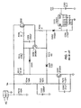
- Fig. 1 shows a conventional catear circuit.
- US 2003/0001516 A1 also shows such a conventional circuit.
- the catear circuit is wired to receive power from a rectifier circuit (RECT), for example, a full wave rectifier, which is wired across a portion of the dimmer circuit to receive rectified AC power.
- RECT rectifier circuit
- the rectifier provides current substantially only during the catear regions because when the triac of the dimmer circuit is on, there is substantially zero voltage across the dimmer.
- a transistor Q206 which may be an FET, is turned on during the catear portions of the rectified AC, i.e., before the triac turns on and after the triac turns off again.
- the gate of transistor Q206 is provided with a voltage sufficient to turn it on via resistors R210, R212 and R220.
- a charging capacitor C262 is charged via resistor R280 and diode D252.
- the output across capacitor C262 is provided to a voltage regulator circuit, for example, a linear regulator U203 which provides a substantially constant DC output to power the circuits connected thereto.
- the charging transistor Q206 conducts to allow charging of the energy storage capacitor C262.
- the rate of charge of the capacitor is determined by resistor R280.
- transistor Q204 When the rectified line voltage exceeds a predetermined value, then transistor Q204 is turned on by the voltage divider formed by resistors R214, R221 and R276. When transistor Q204 turns on, which time can be set by voltage divider circuit comprising resistors R214 and R221 so that it is just prior to the time when the triac of the dimmer circuit turns on, the voltage at the collector of Q204 goes substantially to circuit common, thereby bringing the gate of Q206 substantially to circuit common and turning Q206 off so that Q206 stops charging capacitor C262 during the time when the triac is on.
- capacitor Q262 is utilized as a charge storage element to charge up during the time prior to the triac turning on during the catear portion 1 of the rectified AC line voltage.
- the storage capacitor C262 power for the associated electronic circuits connected to the output of regulator Q203 is provided by the storage capacitor C262.
- a circuit comprising transistor Q252 is also provided to sense an overcurrent condition. Should an overcurrent be detected across resistor R280, transistor Q252 turns on, thus reducing the gate voltage of transistor Q206 to near zero and turning it off.
- a bus regulation circuit comprising zener diode D207 and resistor R275 is provided. If the voltage across storage capacitor C262 rises too high, the zener diode D207 will avalanche, raising the voltage across resistor R276 and turning on Q204 which will thus reduce the gate voltage to transistor Q206, turning it off. Accordingly, if C262 exceeds a predetermined voltage, Q206 will be turned off in that instance also to stop charging C262.
- a power supply circuit comprising: a first switching device having a control terminal and a control terminal switching threshold, the first switching device charging current from a voltage source into a charge storage element, a control circuit controlling an on/off operation of the first switching device whereby the first switching device is turned on when the voltage of the voltage source is below a predetermined level and turned off when the voltage of the voltage source is above the predetermined level, a control voltage supply circuit providing a control voltage to the control terminal of the first switching device substantially in excess of the switching threshold in response to the control circuit when the voltage of the voltage source is below the predetermined voltage thereby to drive the switching device on in a saturated region of operation; and a charge storage element for providing an output voltage of the power supply.
- a catear power supply circuit comprising a first switching transistor having a control terminal and a control terminal switching threshold, the first switching transistor charging current from a voltage source into a charge storage capacitor, a control circuit controlling an on/off operation of the first switching transistor whereby the first switching transistor is enabled to be turned on when the voltage of the voltage source is below a predetermined level and is turned off when the voltage of the voltage source is above the predetermined level, a control voltage supply circuit providing a control voltage substantially in excess of the switching threshold, the control voltage being supplied to the control terminal of the first switching transistor by the control circuit such that when the voltage of the voltage source is below the predetermined level, the control voltage is supplied to the control terminal of the first switching transistor thereby to drive the first switching transistor on in a saturated region of operation and when the voltage of the voltage source is above the predetermined threshold, the control voltage is not supplied to the control terminal, thereby turning the first switching transistor off; and a charge storage capacitor for providing an output voltage of the power supply.
- a lighting dimmer comprising an electronic lamp dimmer circuit providing power to a lamp load, a catear power supply coupled to the electronic lamp dimmer circuit for providing power to electronic circuits of the lighting dimmer, the catear power supply circuit comprising a switching device having a control terminal and a control terminal switching threshold, the switching device charging current from a voltage source into a charge storage element, a control circuit controlling the on/off operation of the switching device whereby the switching device is turned on when the voltage of the voltage source is below a predetermined level and turned off when the voltage of the voltage source is above the predetermined level, a control voltage supply circuit providing a control voltage to the control terminal of the switching device substantially in excess of the switching threshold when the voltage of the voltage source is below the predetermined level thereby to drive the switching device on in a saturated region of operation; and a charge storage element for providing an output voltage of the power supply.
- a method of providing power to an electronic circuit in a two wire dimmer connecting a hot line of an AC network to a lamp load comprising obtaining power from the two wire dimmer during regions of an AC waveform formed across a portion of a circuit of the dimmer when a phase cut switching device of the dimmer providing power to the lamp load is substantially off; driving a switching device providing charging current to a charge storage capacitor on in a saturated region of operation of the switching device when a voltage from a voltage source developed in the dimmer from the AC waveform is less than a predetermined level, and turning the switching device off when the voltage is above the predetermined level, and providing a voltage across the charge storage device as an output voltage.
- the present invention is described herein for use with respect to lamp loads, the invention can also be used with other loads, e.g., motors and other loads.
- loads e.g., motors and other loads.
- various lamps can be employed as loads, and the invention is not limited to incandescent lamp loads but may be used with fluorescent and other gas discharge lamps, without limitation. Further, the invention may be used in "non-dimmer" or other applications where both a hot and neutral are available.
- Fig. 2A shows a dimmer incorporating the power supply (PS) according to the present invention.
- the dimmer includes a triac and its associated dimmer control circuitry as well known to those of skill in the art, as well as additional circuitry to be powered by the power supply.
- the dimmer is wired into the hot side (H) of the AC line and provides a dimmed hot (DH) output to the load comprising a lamp load.
- H hot side
- DH dimmed hot
- the circuit could be employed with other loads, for example, a motor, in which case the speed of the motor is being controlled.
- the neutral (N) of the AC line is not connected to the dimmer so it is not possible to obtain power for the circuits in the dimmer directly across the AC line. Instead, as discussed above, the power supply (PS) must obtain its power across some portion of the dimmer circuit itself.
- Fig. 2B shows how the power supply of Fig. 2A is coupled to the hot AC line and provides power to various low voltage control circuits contained within the dimmer, for example, a microprocessor uP, an RF circuit, various displays and the triac dimmer circuit itself.
- the power supply according to the present invention may be employed with dimmers that incorporate control circuits that receive and provide control and status information via radio frequencies.
- An example of such a system is the Lutron RF seeTouch® system and for less complex systems, the Lutron RadioRA® system. In both of these systems, lighting zones in various parts of a building can be controlled from a central or other locations via radio frequency signals.
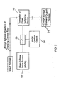
- Fig. 3 is a block diagram of the power supply according to the invention.
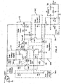
- the circuit includes a switching device 10 coupled to a source of input voltage, a charge storage element 20 providing an output voltage, a control switching device 30 for controlling the on/off operation of the main switching device 10, a control voltage supply circuit comprising a high voltage drive source circuit 40 for driving the charging switch 10 into saturation when the switch 10 is controlled on, and a control circuit 50 for controlling the switching circuit 30 to control the on/off status of switching device 10.
- Switching circuit 10 comprises a switching transistor such as an FET Q11 having its drain connected to a voltage source V+ and its source connected through a resistor R9 and diode D 17 to a charging capacitor C4 in charge of storage circuit 20.
- Voltage source V+ may be provided from a full wave rectifier bridge (RECT), as shown, connected across some portion of the dimmer.
- the gate of transistor Q11 is coupled through resistors R32, R55 and R52 to a high voltage drive source circuit 40.
- the high voltage drive source circuit 40 includes a resistor R49, diode D60, capacitor C16 and a zener diode Z1 connected as shown and coupled between the voltage source V+ and Vc which is the voltage across storage capacitor C4 and ground.
- capacitor C16 may be .1uf
- resistor R49 may be 110 kohms
- diode Z1 may be a 39 volt zener, so that approximately 40V may be developed across C16.
- the control circuit 50 comprises control circuit portions 50A, 50B, 50C and 50D.
- Portion 50A comprises a voltage divider comprising resistors R3 and R4.
- the voltage divider output is connected to the base of a transistor Q14, forming the switching circuit 30.
- the base of transistor Q14 is connected to circuit 50B which comprises a bus regulation circuit connected between the base of transistor Q14 and the anode of diode D17 connected in series with storage capacitor C4.
- control circuit 50 also includes an overcurrent protection and current limiting circuit 50C and a latch circuit 50D.
- Transistor Q11 charges capacitor C4 through resistor R9 and diode D17. Diode D17 prevents discharging of capacitor C4 when Q11 is off.
- the gate of transistor Q11 is provided with gate voltage via gate voltage supply circuit 40 and resistors R52, R55 and R32.
- Gate voltage supply circuit 40 is connected between voltage source V+ and voltage Vc across capacitor C4. Since the voltage across C4 is substantially lower than the voltage on the bus V+, capacitor C16 in circuit 40 immediately begins to charge via resistor R49 and diode D60 as the rectified AC voltage increases during the catear region 1 of Fig. 2 .
- Zener diode Z1 limits the voltage across the capacitor C16 and ensures that the capacitor C16 charges quickly because it acts as a current divider drawing current from V+ to quickly reach its avalanche voltage.
- Capacitor C16 charges quickly through diode D60 and resistor R49, and the voltage across capacitor C16 plus the voltage across capacitor C4 is provided to the gate of transistor Q11 via resistors R52, R55 and R32, driving transistor Q11 into the saturated region very quickly.
- the gate voltage provided to transistor Q11 may be approximately 15 volts, thus quickly driving transistor Q11 into saturation.
- a zener diode Z2 is provided to prevent the gate voltage from exceeding a predetermined safe level to protect FET Q11, for example, to maintain the gate voltage below about 25 volts.
- Diode D60 prevents discharge of capacitor C16 when voltage V+ drops to near zero when the triac turns on.
- transistor Q11 Once transistor Q11 goes on, it is in its saturated region and the capacitor C4 is charged with minimal loss in transistor Q11.
- the charged voltage across capacitor C4 is provided to a voltage regulator U2, for example, a conventional linear regulator, similarly as in the prior art, and the output of U2 is provided to power the various electronic circuits.
- Transistor Q14 performs the function of switch 30 in the block diagram of Fig. 3 . As soon as the voltage V+ exceeds a predetermined level, Q14 is turned on (the triac turns on at some time thereafter), thus driving the gate of Q11 low via resistors R55 and R32, and turning Q11 off, preventing charging during the period of time when the dimmer triac turns on, thereby preventing drawing current away from the dimmer and lamp load during this time.
- Transistor Q14 is turned on by the voltage divider circuit 50A comprising resistors R3 and R4.
- circuit 50D includes a latch circuit comprising transistor Q25.
- the transistor Q25 is a PNP transistor.
- Q25 functions to latch transistor Q14 on and therefore the FET Q11 off.
- the collector voltage of Q14 drops.
- the collector of Q14 is connected to the base PNP transistor Q25 by resistor R54.
- Q25 turns on thereby increasing the voltage drop across resistor R4 thus ensuring that transistor Q14 latches on.
- Circuit 50 also includes circuit 50B which comprises a bus regulation circuit. Should the voltage across capacitor C4 increase above a preset level, zener diode Z3 avalanches, thereby increasing the voltage across the resistor R4 and turning transistor Q14 on. This could occur, for example, during the catear portions of the input waveform (regions 1 and 3 of Fig. 2 ) when capacitor C4 is charging should the charging voltage across capacitor C4 increase to levels above a predetermined voltage.
- Circuit 50 also includes an overcurrent protection and current limiting circuit 50C.
- Resistor R9 limits the current through the FET at all times.
- transistor Q26 is connected to resistor R9 such that should the voltage across resistor R9 exceed the threshold of Q26, transistor Q26 will turn on thereby driving the gate of transistor Q11 toward its source and turning transistor Q11 off in the event of an overcurrent.
- the voltage across bus V+ is determined by the catear waveform of region 3 of Fig. 2 , and, as soon as the voltage V+ drops below a certain level so that voltage divider 50A provides a voltage insufficient to keep transistor Q14 on, Q14 turns off, thus turning on Q11 and again charging current into capacitor C4 during catear region 3 of Fig. 2 .
- the present invention thus provide a power supply of the catear type which is highly efficient because losses in the switching device charging the charge storage element are reduced by ensuring that the switching device, when on, is operating in its saturated region.
- prior art catear topologies turn the switching device on in dependence on the AC line voltage which dissipates considerably more energy since the FET is not saturated but instead operating in its linear region.
- the present invention provides for FET saturation at low line voltages, which leads to greater efficiency.
- Another advantage of the present circuit over other possible power supply circuits is that the switching device operates at a low frequency.
- prior art switching power supplies operate at high frequencies creating substantial RF noise which can interfere with RF control circuits with which the present invention can operate as well as generally radiating substantial EMI which must be shielded or otherwise reduced.
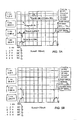
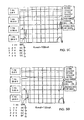
- Figs. 5A-5E show waveforms of the gate-drain voltage across FET Q11, the voltage across capacitor C4, the input current into the rectifier and the gate voltage of FET Q11 measured between the gate and the circuit common ground connection. Each waveform is based upon a network voltage of 120 volts AC.
- Fig. 5A is for a load current of 50 mA;
- Fig. 5B shows the waveforms for a load of 75 mA;
- Fig. 5C shows the waveform for a load of 100 mA;
- Fig. 5D shows the waveforms for a load of 125 mA; and
- Fig. 5E shows the waveforms for a load of 150 mA.
- the gate waveform to transistor Q11 has a very sharply defined rising edge with the voltage rising quickly to about 15 volts, thus driving the FET Q11 into saturation very quickly.
- the gate voltage rises high enough to turn the FET on quickly into saturation.
- the V+ voltage bus ranges from about 50 volts down to about 45 volts.
- the capacitor bus voltage across capacitor C4 ranges between 8.5 to 7.5 volts at 150 mA load and the input current essentially follows the line current.
Landscapes
- Engineering & Computer Science (AREA)
- Power Engineering (AREA)
- Power Conversion In General (AREA)
- Dc-Dc Converters (AREA)
- Circuit Arrangement For Electric Light Sources In General (AREA)
- Charge And Discharge Circuits For Batteries Or The Like (AREA)
Claims (44)
- Stromversorgungskreis, umfassend:ein erstes Schaltgerät (10), welches ein Steuerungsterminal und eine Schaltschwelle für das Steuerungsterminal aufweist, wobei das erste Schaltgerät (10) Strom aus einer Spannungsquelle in ein Ladungsspeicherelement (20) lädt, gekennzeichnet durch
eine Steuerschaltung (50), die einen Ein-/Ausschaltvorgang des ersten Schaltgeräts (10) steuert, wodurch das erste Schaltgerät (10) eingeschaltet wird, wenn die Spannung der Spannungsquelle unter einem vorgegebenen Wert liegt, und ausgeschaltet wird, wenn die Spannung der Spannungsquelle über dem vorgegebenen Wert liegt,
eine Versorgungsschaltung (40) für eine Steuerspannung, die eine Steuerspannung an das Steuerungsterminal des ersten Schaltgeräts (10) liefert, die in Reaktion auf die Steuerschaltung (50) im Wesentlichen über der Schaltschwelle liegt, wenn die Spannung der Spannungsquelle unter dem vorgegebenen Wert liegt, um dadurch das Schaltgerät (10) in einem gesättigten Betriebsbereich einzuschalten, und
das Ladungsspeicherelement (20), um eine Ausgangsspannung der Stromversorgung zu liefern. - Stromversorgungskreis nach Anspruch 1, wobei die Steuerschaltung ein zweites Schaltgerät umfasst, das durch die Spannungsquelle gesteuert wird, wodurch, wenn die Spannung der Spannungsquelle den vorgegebenen Wert übersteigt, das zweite Schaltgerät Strom weg von dem Steuerungsterminal des ersten Schaltgeräts lenkt, wodurch das erste Schaltgerät ausgeschaltet wird.
- Stromversorgungskreis nach Anspruch 1, ferner einen verriegelnden Schalter umfassend, der an das zweite Schaltgerät gekoppelt ist, um das zweite Schaltgerät eingeschaltet zu versiegeln, um Strom weg von dem Steuerungsterminal zu dem ersten Schaltgerät zu lenken, um das zweite Schaltgerät eingeschaltet zu halten und dadurch das erste Schaltgerät ausgeschaltet zu halten.
- Stromversorgungskreis nach Anspruch 1, ferner eine Schaltung zur Regelung der Spannung des Ladungsspeicherelements umfassend, um eine Spannung über dem Ladungsspeicherelement unter einem voreingestellten Wert zu halten.
- Stromversorgungskreis nach Anspruch 4, wobei die Schaltung zur Regelung der Spannung des Ladungsspeicherelements das zweite Schaltgerät einschaltet, um Strom weg von dem Steuerungsterminal des ersten Schaltgeräts zu lenken, wenn die Spannung über dem Ladungsspeicherelement den voreingestellten Wert übersteigt.
- Stromversorgungskreis nach Anspruch 1, ferner eine Überstromschutzschaltung umfassend, die an das erste Schaltgerät gekoppelt ist, um den Ladestrom durch das erste Schaltgerät in das Ladungsspeicherelement zu begrenzen.
- Stromversorgungskreis nach Anspruch 6, wobei die Überstromschutzschaltung ein drittes Schaltgerät umfasst, das sich einschaltet, um Strom weg von dem Steuerungsterminal zu lenken, wenn der Ladestrom durch das erste Schaltgerät einen voreingestellten Stromwert übersteigt.
- Stromversorgungskreis nach Anspruch 1, ferner einen Spannungsregler umfassend, der an das Ladungsspeicherelement gekoppelt ist und die Ausgangsspannung liefert.
- Stromversorgungskreis nach Anspruch 1, wobei die Versorgungsschaltung für die Steuerspannung ein RC-Netzwerk umfasst, welches einen Widerstand und einen Kondensator umfasst, wobei eine über dem Kondensator anstehende Spannung an das Steuerungsterminal des ersten Schaltgeräts gekoppelt ist, um das erste Schaltgerät in den gesättigten Betriebsbereich zu bringen.
- Stromversorgungskreis nach Anspruch 9, wobei die Versorgungsschaltung für die Steuerspannung ferner ein Lawinengerät umfasst, welches an den Kondensator gekoppelt ist, um die Spannung, die an dem Kondensator anstehen kann, zu begrenzen.
- Stromversorgungskreis nach Anspruch 10, wobei der Kondensator zwischen der Spannungsquelle und dem Ladungsspeicherelement gekoppelt ist.
- Stromversorgungskreis nach Anspruch 1, ferner ein spannungsempfindliches Schutz gerät umfassend, welches an das Steuerungsterminal des ersten Schaltgeräts gekoppelt ist, um die an dem Steuerungsterminal anliegende Spannung zu begrenzen.
- Stromversorgungskreis nach Anspruch 1, wobei das erste Schalt gerät einen FET umfasst.
- Stromversorgungskreis nach Anspruch 9, wobei die Versorgungsschaltung für die Steuerspannung ferner eine Diode umfasst, die mit dem Kondensator in Reihe geschaltet ist, um eine Entladung des Kondensators der Versorgungsschaltung für die Steuerspannung zu der Spannungsquelle zu verhindern.
- Stromversorgungskreis nach Anspruch 1, ferner eine Diode umfassend, die mit dem Ladungsspeicherelement in Reihe gekoppelt ist, um eine Entladung des Ladungsspeicherelements zu verhindern. wenn das erste Schaltgerät ausgeschaltet ist.
- Stromversorgungskreis nach Anspruch 1, wobei das Ladungsspeicherelement einen Kondensator umfasst.
- Stromversorgungskreis nach Anspruch 2, wobei das zweite Schaltgerät ein Steuerungsterminal aufweist, welches an eine Widerstandsteilerschaltung gekoppelt ist, wobei die Widerstandsteilerschaltung zwischen der Spannungsquelle und einem gemeinsamen Terminal für den Stromversorgungskreis gekoppelt ist.
- Stromversorgungskreis nach einem der Ansprüche 1 bis 17 als "Cat-Ear"-Stromversorgungskreis, umfassend:einen ersten Schalttransistor (Q11), welcher das Steuerungsterminal und die Schaltschwelle für das Steuerungsterminal aufweist, wobei der erste Schalttransistor (Q11) Strom aus der Spannungsquelle (V+) in einen Ladungsspeicherkondensator (C4) lädt,die Steuerschaltung (50), welche einen Ein-/Ausschaltvorgang des ersten Schalttransistors (40) steuert, wodurch es möglich wird, dass der erste Schalttransistor (40) eingeschaltet wird, wenn die Spannung der Spannungsquelle (V+) unter dem vorgegebenen Wert liegt, und ausgeschaltet wird, wenn die Spannung der Spannungsquelle (V+) über dem vorgegebenen Wert liegt,die Versorgungsschaltung (40) für die Steuerspannung, welche die Steuerspannung im Wesentlichen über der Schaltschwelle liefert, wobei die Steuerspannung durch die Steuerschaltung (50) auf eine solche Weise zu dem Steuerungsterminal des ersten Schalttransistors (Q11) geleitet wird, dass, wenn die Spannung der Spannungsquelle (V+) unter dem vorgegebenen Wert liegt, die Steuerspannung zu dem Steuerungsterminal des ersten Schalttransistors (Q11) geleitet wird, um dadurch den ersten Schalttransistor (Q11) in einem gesättigten Betriebsbereich einzuschalten und, wenn die Spannung der Spannungsquelle (V+) über der vorgegebenen Schwelle liegt, die Steuerspannung nicht zu dem Steuerungsterminal geleitet wird, wodurch der erste Schalttransistor (Q11) ausgeschaltet wird, undden Ladungsspeicherkondensator (C4), um die Ausgangsspannung der Stromversorgung zu liefern.
- "Cat-Ear"-Stromversorgungskreis nach Anspruch 18, wobei die Steuerschaltung einen zweiten Schalttransistor umfasst, der durch die Spannungsquelle gesteuert wird, wodurch, wenn der Wert der Spannungsquelle den vorgegebenen Wert übersteigt, der zweite Schalttransistor Strom weg von dem Steuerungsterminal des ersten Schalttransistors lenkt, wodurch der erste Schalttransistor ausgeschaltet wird.
- "Cat-Ear"-Stromversorgungskreis nach Anspruch 18, ferner einen verriegelnden Transistor umfassend, der an den zweiten Schalttransistor gekoppelt ist, um den zweiten Schalttransistor eingeschaltet zu verriegeln, um Strom weg von dem Steuerungsterminal des ersten Schalttransistors zu lenken, um den zweiten Schalttransistor eingeschaltet zu halten und dadurch den ersten Schalttransistor ausgeschaltet zu halten.
- "Cat-Ear"-Stromversorgungskreis nach Anspruch 18, ferner eine Schaltung zur Regelung der Spannung des Ladungsspeicherkondensators umfassend, um eine Spannung über dem Ladungsspeicherkondensator unter einem voreingestellten Wert zu halten.
- "Cat-Ear"-Stromversorgungskreis nach Anspruch 21, wobei die Schaltung zur Regelung der Spannung des Ladungsspeicherkondensators den zweiten Schalttransistor einschaltet, um Strom weg von dem Steuerungsterminal des ersten Schalttransistors zu lenken, wenn die Spannung über dem Ladungsspeicherkondensator den voreingestellten Wert übersteigt.
- "Cat-Ear"-Stromversorgungskreis nach Anspruch 18, ferner eine Überstromschutzschaltung umfassend, die an den ersten Schalttransistor gekoppelt ist, um den Ladestrom durch den ersten Schalttransistor in den Ladungsspeicherkondensator zu begrenzen.
- "Cat-Ear"-Stromversorgungskreis nach Anspruch 23, wobei die Überstromschutzschaltung einen dritten Schalttransistor umfasst, der sich einschaltet, um Strom weg von dem Steuerungsterminal zu lenken, wenn der Ladestrom durch den ersten Schalttransistor einen voreingestellten Stromwert übersteigt.
- "Cat-Ear"-Stromversorgungskreis nach Anspruch 18, ferner einen Spannungsregler umfassend, der an den Ladungsspeicherkondensator gekoppelt ist und die Ausgangsspannung liefert.
- "Cat-Ear"-Stromversorgungskreis nach Anspruch 18, wobei die Versorgungsschaltung für die Steuerspannung ein RC-Netzwerk umfasst, welches einen Widerstand und einen Kondensator umfasst, wobei eine über dem Kondensator anstehende Spannung an das Steuerungsterminal des ersten Schalttransistors gekoppelt ist, um den ersten Schalttransistor in den gesättigten Betriebsbereich zu bringen.
- "Cat-Ear"-Stromversorgungskreis nach Anspruch 26, wobei die Versorgungsschaltung für die Steuerspannung ein Lawinengerät umfasst, das an den Kondensator gekoppelt ist, um die Spannung, die über dem Kondensator anstehen kann, zu begrenzen.
- "Cat-Ear"-Stromversorgungskreis nach Anspruch 27, wobei der Kondensator zwischen der Spannungsquelle und dem Ladungsspeicherkondensator gekoppelt ist.
- "Cat-Ear"-Stromversorgungskreis nach Anspruch 18, ferner ein spannungsempfindliches Schutzgerät umfassend, das an das Steuerungsterminal des ersten Schalttransistors gekoppelt ist, um die an dem Steuerungsterminal anliegende Spannung zu begrenzen.
- "Cat-Ear"-Stromversorgungskreis nach Anspruch 18, wobei der erste Schalttransistor einen FET umfasst.
- "Cat-Ear"-Stromversorgungskreis nach Anspruch 26, wobei die Versorgungsschaltung für die Steuerspannung ferner eine Diode umfasst, die mit dem Kondensator in Reihe geschaltet ist, um eine Entladung des Kondensators der Versorgungsschaltung für die Steuerspannung zu der Spannungsquelle zu verhindern.
- "Cat-Ear"-Stromversorgungskreis nach Anspruch 18, ferner eine Diode umfassend, die mit dem Ladungsspeicherkondensator in Reihe gekoppelt ist, um eine Entladung des Ladungsspeicherkondensators zu verhindern, wenn der erste Schalttransistor ausgeschaltet ist.
- "Cat-Ear"-Stromversorgungskreis nach Anspruch 19, wobei der zweite Schalttransistor ein Steuerungsterminal aufweist, das an eine Widerstandsteilerschaltung gekoppelt ist, wobei die Widerstandsteilerschaltung zwischen der Spannungsquelle und einem gemeinsamen Terminal für den Stromversorgungskreis gekoppelt ist.
- Lichtregler, umfassend:eine elektronische Lampenlichtreglerschaltung, welche eine Lampenlast mit Strom versorgt,eine Stromversorgung nach einem der Ansprüche 1 bis 33 als "Cat-Ear"-Stromversorgung, die an die elektronische Lampenlichtreglerschaltung gekoppelt ist, um elektronische Schaltungen des Lichtreglers mit Strom zu versorgen, wobei der "Cat-Ear"-Stromversorgungskreis Folgendes umfasst:das Schaltgerät (10), welches das Steuerungsterminal und die Schaltschwelle für das Steuerungsterminal aufweist, wobei das Schaltgerät (10) Strom von der Spannungsquelle in das Ladungsspeicherelement (20) lädt,die Steuerschaltung (50), welche den Ein-/Ausschaltvorgang des Schaltgeräts (10) steuert, wodurch das Schaltgerät (10) eingeschaltet wird, wenn die Spannung der Spannungsquelle unter dem vorgegebenen Wert liegt, und ausgeschaltet wird, wenn die Spannung der Spannungsquelle über dem vorgegebenen Wert liegt,die Versorgungsschaltung (40) für die Steuerspannung, welche dem Steuerungsterminal des Schaltgeräts (10) die Steuerspannung im Wesentlichen über der Schaltschwelle liefert, wenn die Spannung der Spannungsquelle unter dem vorgegebenen Wert liegt, um dadurch das Schaltgerät (10) in dem gesättigten Betriebsbereich einzuschalten,und das Ladungsspeicherelement (20), um die Ausgangsspannung der Stromversorgung zu liefern.
- Lichtregler nach Anspruch 34, wobei die Lampenlichtreglerschaltung einen Triac beinhaltet.
- Lichtregler nach Anspruch 34, wobei die elektronischen Schaltungen wenigstens einen Mikroprozessor und/oder eine Anzeige beinhalten.
- Lichtregler nach Anspruch 34, wobei die elektronischen Schaltungen eine RF-Schaltung beinhalten.
- Lichtregler nach Anspruch 34, wobei die elektronischen Schaltungen eine elektronische Lampenlichtreglerschaltung beinhalten.
- Verfahren für die Lieferung von Strom zu einer elektronischen Schaltung in einem Zweidraht-Lichtregler, der eine spannungsführende Leitung eines Wechselstromnetzes mit einer Lampenlast verbindet, wobei das Verfahren Folgendes umfasst:Empfangen von Strom von dem Zweidraht-Lichtregler in Bereichen eines Wechselstromschwingungsverlaufs, der über einen Abschnitt eines Stromkreises des Lichtreglers gebildet wird, wenn ein Phasentrennschaltgerät des Lichtreglers, das die Lampenlast mit Strom versorgt, im Wesentlichen ausgeschaltet ist,Einschalten eines Schaltgeräts, das Ladestrom zu einem Ladungsspeicherkondensator liefert, in einem gesättigten Betriebsbereich des Schaltgeräts, wenn eine Spannung aus einer Spannungsquelle, die in dem Lichtregler aus dem Wechselstromschwingungsverlauf ansteht, unter einem vorgegebenen Wert liegt, und Ausschalten des Schaltgeräts, wenn die Spannung über dem vorgegebenen Wert liegt, undLiefern einer Spannung über dem Ladungsspeichergerät als Ausgangsspannung.
- Verfahren nach Anspruch 39, wobei der Schritt des Einschaltens des Schaltgeräts in einem gesättigten Betriebsbereich das Erzeugen einer Spannung über einem Kondensator und das Liefern der Spannung über dem Kondensator zu einer Steuerelektrode des Schaltgeräts umfasst, um das Schaltgerät in den gesättigten Betriebsbereich zu bringen.
- Verfahren nach Anspruch 40, wobei der Schritt des Erzeugens einer Spannung über einem Kondensator das Liefern einer gleichgerichteten Gleichstromspannung umfasst, um den Kondensator zu laden und die Spannung über dem Kondensator zu begrenzen.
- Verfahren nach Anspruch 39, wobei der Schritt des Einschaltens des Schaltgeräts das Einschalten des Schaltgeräts umfasst, indem an ein Steuerungsteiminal des Schaltgeräts eine Steuerspannung geliefert wird, die im Wesentlichen über einer Steuerungsterminalschwellenspannung des Schaltgeräts liegt.
- Verfahren nach Anspruch 42, wobei die Steuerspannung ungefähr 15 Volt beträgt.
- Verfahren nach Anspruch 39, ferner das Regeln der Ausgangsspannung des Ladungsspeichergeräts umfassend.
Applications Claiming Priority (2)
| Application Number | Priority Date | Filing Date | Title |
|---|---|---|---|
| US10/458,608 US7091672B2 (en) | 2003-06-10 | 2003-06-10 | High efficiency off-line linear power supply |
| PCT/US2004/018304 WO2004112225A2 (en) | 2003-06-10 | 2004-06-08 | High efficiency off-line linear power supply |
Publications (3)
| Publication Number | Publication Date |
|---|---|
| EP1636660A2 EP1636660A2 (de) | 2006-03-22 |
| EP1636660A4 EP1636660A4 (de) | 2007-07-04 |
| EP1636660B1 true EP1636660B1 (de) | 2016-01-13 |
Family
ID=33510616
Family Applications (1)
| Application Number | Title | Priority Date | Filing Date |
|---|---|---|---|
| EP04754802.9A Expired - Lifetime EP1636660B1 (de) | 2003-06-10 | 2004-06-08 | Hocheffiziente offline-linearstromversorgung |
Country Status (6)
| Country | Link |
|---|---|
| US (3) | US7091672B2 (de) |
| EP (1) | EP1636660B1 (de) |
| JP (1) | JP2007516687A (de) |
| CN (2) | CN102916580A (de) |
| CA (1) | CA2528977C (de) |
| WO (1) | WO2004112225A2 (de) |
Families Citing this family (55)
| Publication number | Priority date | Publication date | Assignee | Title |
|---|---|---|---|---|
| EP1732247A4 (de) * | 2004-03-03 | 2011-05-04 | Nec Corp | Positionierungssystem, positionierungsmethode, und programm daraus |
| US6972921B1 (en) | 2004-04-05 | 2005-12-06 | Marvell International Ltd. | Circuit and method for protecting emergency head-retract |
| EP1754304A4 (de) * | 2004-05-24 | 2008-05-28 | Young-Chang Cho | Verfahren zur regelung von niederspannung unter verwendung von wellen-ac und system zu seiner durchführung |
| US7740861B2 (en) | 2004-06-16 | 2010-06-22 | University Of Massachusetts | Drug delivery product and methods |
| ES2375995T3 (es) | 2004-09-17 | 2012-03-08 | University Of Massachusetts | Composiciones y sus usos para deficiencias de enzima lisosomal. |
| MX2008000321A (es) | 2005-06-30 | 2008-03-11 | Lutron Electronics Co | Reductor de luz que tiene un suministro de energia controlado por un microprocesador. |
| US8892913B2 (en) | 2005-06-30 | 2014-11-18 | Lutron Electronics Co., Inc. | Load control device having a low-power mode |
| EP1748538A1 (de) * | 2005-07-29 | 2007-01-31 | STMicroelectronics S.r.l. | Schaltnetzteil mit Spannungsbegrenzungsvorrichtung und Verfahren für dessen Steuerung |
| US7489088B2 (en) * | 2005-10-27 | 2009-02-10 | Leviton Manufacturing Co., Ltd. | Power supply for 2-line dimmer |
| US7411768B2 (en) * | 2006-05-30 | 2008-08-12 | Harris Corporation | Low-loss rectifier with shoot-through current protection |
| DE602007009381D1 (de) * | 2007-08-23 | 2010-11-04 | Niko Nv | Dimmer mit Ladungspumpe |
| EP2222283A2 (de) | 2007-10-29 | 2010-09-01 | University of Massachusetts | Zur freisetzung von nukleinsäuren (sirna) mit hefe-zellwandproteinen verkapselte mehrlagige nanopatikel |
| US8067926B2 (en) | 2007-12-21 | 2011-11-29 | Lutron Electronics Co., Inc. | Power supply for a load control device |
| GB2458704A (en) * | 2008-03-28 | 2009-09-30 | Bombardier Transp Gmbh | An improved overcurrent protection circuit for an IGBT in an inverter |
| GB2458699A (en) * | 2008-03-28 | 2009-09-30 | Deepstream Technologies Ltd | Linear regulator with zero crossing coordination |
| US20110115454A1 (en) * | 2008-04-08 | 2011-05-19 | Benedict Melvin K | Voltage regulator |
| US7889526B2 (en) * | 2008-05-02 | 2011-02-15 | Lutron Electronics Co., Inc. | Cat-ear power supply having a latch reset circuit |
| AU2008217015B2 (en) * | 2008-09-15 | 2011-04-14 | Quan Mei Technology Co., Ltd. | Current-regulated light emitting device for vehicle use |
| GB2467591B (en) * | 2009-02-09 | 2013-06-26 | Novar Ed & S Ltd | Dimmer protection |
| US8866401B2 (en) * | 2009-03-06 | 2014-10-21 | Lutron Electronics Co., Inc. | Multi-stage power supply for a load control device having a low-power mode |
| US7960922B2 (en) * | 2009-10-21 | 2011-06-14 | General Electric Company | High efficiency low power capacitor charged DC driver |
| US8686668B2 (en) | 2009-10-26 | 2014-04-01 | Koninklijke Philips N.V. | Current offset circuits for phase-cut power control |
| US9160224B2 (en) | 2009-11-25 | 2015-10-13 | Lutron Electronics Co., Inc. | Load control device for high-efficiency loads |
| US8988050B2 (en) * | 2009-11-25 | 2015-03-24 | Lutron Electronics Co., Inc. | Load control device for high-efficiency loads |
| US8957662B2 (en) | 2009-11-25 | 2015-02-17 | Lutron Electronics Co., Inc. | Load control device for high-efficiency loads |
| US11870334B2 (en) | 2009-11-25 | 2024-01-09 | Lutron Technology Company Llc | Load control device for high-efficiency loads |
| US8750007B2 (en) * | 2010-03-23 | 2014-06-10 | Qualcomm Incorporated | Power conversion |
| JP5457927B2 (ja) * | 2010-04-23 | 2014-04-02 | セミコンダクター・コンポーネンツ・インダストリーズ・リミテッド・ライアビリティ・カンパニー | 発光素子の制御回路 |
| JP5645109B2 (ja) * | 2010-07-27 | 2014-12-24 | パナソニックIpマネジメント株式会社 | 2線式負荷制御装置 |
| US8334663B2 (en) | 2010-07-30 | 2012-12-18 | Lutron Electronics Co., Inc. | Power supply for a load control device |
| US9588161B2 (en) * | 2010-12-07 | 2017-03-07 | Desco Industries, Inc. | Ionization balance device with shielded capacitor circuit for ion balance measurements and adjustments |
| CN102592328B (zh) * | 2011-01-14 | 2014-07-02 | 金宝电子工业股份有限公司 | 离线设定记录装置及方法与其电子装置 |
| US9258863B2 (en) | 2011-08-19 | 2016-02-09 | Marvell World Trade Ltd. | Method and apparatus for TRIAC applications |
| WO2013027121A1 (en) | 2011-08-19 | 2013-02-28 | Marvell World Trade, Ltd. | Protection circuit in triac applications |
| CN104115350A (zh) | 2011-12-08 | 2014-10-22 | 3M创新有限公司 | 电离监测装置和方法 |
| CN102761252B (zh) * | 2012-07-25 | 2015-05-27 | 广州视源电子科技股份有限公司 | 带有切换mos管的开关电源电路 |
| US8917076B2 (en) * | 2012-08-10 | 2014-12-23 | Monolithic Power Systems, Inc. | Off-line regulator with pass device and associated method |
| CN103997237B (zh) * | 2014-05-27 | 2016-07-06 | 深圳创维-Rgb电子有限公司 | 大功率电源供电系统 |
| US20160043653A1 (en) | 2014-05-28 | 2016-02-11 | Smart Fos, Inc. | Systems and Methods for a Transformerless Power Supply to Limit Heat Generation at an Output Transistor Via Timed Current Draws |
| JP6938620B2 (ja) * | 2016-05-07 | 2021-09-22 | インテレソル,エルエルシー | 高効率ac−dcコンバータおよび方法 |
| EP3533140B1 (de) * | 2016-10-28 | 2024-06-05 | Intelesol, LLC | Hocheffizienter wechselstrom-direkt-zu-gleichstrom-extraktionsumrichter und verfahren |
| US11056981B2 (en) | 2018-07-07 | 2021-07-06 | Intelesol, Llc | Method and apparatus for signal extraction with sample and hold and release |
| US11581725B2 (en) | 2018-07-07 | 2023-02-14 | Intelesol, Llc | Solid-state power interrupters |
| US11671029B2 (en) * | 2018-07-07 | 2023-06-06 | Intelesol, Llc | AC to DC converters |
| US11205011B2 (en) | 2018-09-27 | 2021-12-21 | Amber Solutions, Inc. | Privacy and the management of permissions |
| US11334388B2 (en) | 2018-09-27 | 2022-05-17 | Amber Solutions, Inc. | Infrastructure support to enhance resource-constrained device capabilities |
| US10985548B2 (en) | 2018-10-01 | 2021-04-20 | Intelesol, Llc | Circuit interrupter with optical connection |
| US11349296B2 (en) | 2018-10-01 | 2022-05-31 | Intelesol, Llc | Solid-state circuit interrupters |
| KR102857286B1 (ko) | 2018-12-17 | 2025-09-08 | 인테레솔, 엘엘씨 | Ac 구동 발광 다이오드 시스템 |
| US11348752B2 (en) | 2019-05-18 | 2022-05-31 | Amber Solutions, Inc. | Intelligent circuit breakers with air-gap and solid-state switches |
| JP7554272B2 (ja) | 2020-01-21 | 2024-09-19 | アンバー セミコンダクター,インク. | インテリジェント回路遮断 |
| EP4197086A4 (de) | 2020-08-11 | 2024-09-04 | Amber Semiconductor, Inc. | Intelligentes energiequellenüberwachungs- und auswahlsteuersystem |
| US12113525B2 (en) | 2021-09-30 | 2024-10-08 | Amber Semiconductor, Inc. | Intelligent electrical switches |
| US12348028B2 (en) | 2021-10-22 | 2025-07-01 | Amber Semiconductor, Inc. | Multi-output programmable power manager |
| US12362646B2 (en) | 2022-01-26 | 2025-07-15 | Amber Semiconductor, Inc. | Controlling AC power to inductive loads |
Family Cites Families (39)
| Publication number | Priority date | Publication date | Assignee | Title |
|---|---|---|---|---|
| US2810105A (en) * | 1953-05-19 | 1957-10-15 | Sorenson & Company Inc | Voltage regulator |
| US3068392A (en) * | 1958-05-22 | 1962-12-11 | Krohn Hite Lab Inc | Power supply |
| US3373344A (en) * | 1964-09-14 | 1968-03-12 | Rca Corp | Voltage regulator circuit including a storage capacitor and a switching means responsive to a voltage difference for charging the capacitor |
| US3460023A (en) * | 1967-03-27 | 1969-08-05 | Applied Dynamics Inc | Regulated power supply |
| US3581187A (en) * | 1969-06-23 | 1971-05-25 | Metrodynamics Corp | Regulated dc power supply |
| US4001668A (en) * | 1973-11-16 | 1977-01-04 | Schick Incorporated | Electric shaver operable from a wide range of supply voltages |
| JPS5790722A (en) | 1980-11-27 | 1982-06-05 | Omron Tateisi Electronics Co | Dc power supply circuit |
| US4430608A (en) * | 1981-12-22 | 1984-02-07 | Hughes Aircraft Company | Base drive circuit |
| US4580090A (en) * | 1983-09-16 | 1986-04-01 | Motorola, Inc. | Maximum power tracker |
| US4521725A (en) * | 1983-12-02 | 1985-06-04 | United Technologies Corporation | Series switching regulator |
| US4553082A (en) | 1984-05-25 | 1985-11-12 | Hughes Aircraft Company | Transformerless drive circuit for field-effect transistors |
| US4685046A (en) | 1985-10-03 | 1987-08-04 | The Scott & Fetzer Company | Low voltage direct current power supply |
| US4733159A (en) | 1986-10-28 | 1988-03-22 | Motorola, Inc. | Charge pump voltage regulator |
| US4864482A (en) * | 1988-07-07 | 1989-09-05 | Etta Industries, Inc. | Conversion circuit for limiting inrush current |
| US5105144A (en) * | 1991-02-01 | 1992-04-14 | Honeywell Inc. | Driver for field effect transistor |
| EP0500113B1 (de) * | 1991-02-22 | 1997-12-17 | Matsushita Electric Industrial Co., Ltd. | Stromversorgungseinheit |
| US5469046A (en) * | 1993-04-30 | 1995-11-21 | North American Philips Corporation | Transformerless low voltage switching power supply |
| DE9416084U1 (de) * | 1993-10-25 | 1995-02-23 | Papst-Motoren GmbH & Co. KG, 78112 St Georgen | Netzgerät |
| US5500575A (en) * | 1993-10-27 | 1996-03-19 | Lighting Control, Inc. | Switchmode AC power controller |
| JP3126565B2 (ja) * | 1993-11-01 | 2001-01-22 | 株式会社東芝 | Ac/dc変換器 |
| EP0782786A1 (de) * | 1994-09-21 | 1997-07-09 | Abbott Laboratories | Spannungswandler mit hohem wirkungsgrad und reglerschaltung |
| US5773965A (en) * | 1995-10-24 | 1998-06-30 | Rohm Co., Ltd. | Switching power supply apparatus for converting a high DC voltage into a low DC voltage |
| US5818708A (en) * | 1996-12-12 | 1998-10-06 | Philips Electronics North America Corporation | High-voltage AC to low-voltage DC converter |
| US5920183A (en) * | 1997-10-24 | 1999-07-06 | Stmicroelectronics, Inc. | Voltage regulator for regulating its output voltage selectively with respect to more than one voltage |
| US6346778B1 (en) * | 1998-01-20 | 2002-02-12 | Bytecraft Pty Ltd | AC power converter |
| US6710546B2 (en) * | 1998-10-30 | 2004-03-23 | The Bodine Company, Inc. | Remote control test apparatus |
| US6828733B1 (en) * | 1998-10-30 | 2004-12-07 | David B. Crenshaw | Remote lamp control apparatus |
| US6061259A (en) * | 1999-08-30 | 2000-05-09 | Demichele; Glenn | Protected transformerless AC to DC power converter |
| US6320363B1 (en) * | 1999-12-17 | 2001-11-20 | Motorola, Inc. | Voltage regulator with improved transient response |
| US6486616B1 (en) * | 2000-02-25 | 2002-11-26 | Osram Sylvania Inc. | Dual control dimming ballast |
| JP2002091584A (ja) * | 2000-09-19 | 2002-03-29 | Rohm Co Ltd | 電気機器 |
| US6452766B1 (en) * | 2000-10-30 | 2002-09-17 | National Semiconductor Corporation | Over-current protection circuit |
| US6275395B1 (en) * | 2000-12-21 | 2001-08-14 | Micrel, Incorporated | Accelerated turn-off of MOS transistors by bootstrapping |
| US6674248B2 (en) * | 2001-06-22 | 2004-01-06 | Lutron Electronics Co., Inc. | Electronic ballast |
| US7285919B2 (en) * | 2001-06-22 | 2007-10-23 | Lutron Electronics Co., Inc. | Electronic ballast having improved power factor and total harmonic distortion |
| US6969959B2 (en) * | 2001-07-06 | 2005-11-29 | Lutron Electronics Co., Inc. | Electronic control systems and methods |
| JP2003047150A (ja) * | 2001-07-27 | 2003-02-14 | Denso Corp | 電源回路 |
| US6724157B2 (en) * | 2001-11-14 | 2004-04-20 | Astral Communications Inc. | Energy savings device and method for a resistive and/or an inductive load |
| US6906477B2 (en) * | 2003-10-14 | 2005-06-14 | Astral Communications, Inc. | Linear control device for controlling a resistive and/or an inductive and/or a capacitive load |
-
2003
- 2003-06-10 US US10/458,608 patent/US7091672B2/en not_active Expired - Lifetime
-
2004
- 2004-06-08 WO PCT/US2004/018304 patent/WO2004112225A2/en not_active Ceased
- 2004-06-08 EP EP04754802.9A patent/EP1636660B1/de not_active Expired - Lifetime
- 2004-06-08 CN CN201210399090.7A patent/CN102916580A/zh active Pending
- 2004-06-08 JP JP2006533644A patent/JP2007516687A/ja not_active Withdrawn
- 2004-06-08 CN CN200480022996.0A patent/CN1836193A/zh active Pending
- 2004-06-08 CA CA2528977A patent/CA2528977C/en not_active Expired - Fee Related
-
2006
- 2006-06-26 US US11/474,713 patent/US7446486B2/en not_active Expired - Fee Related
-
2008
- 2008-10-22 US US12/256,137 patent/US7952300B2/en not_active Expired - Fee Related
Also Published As
| Publication number | Publication date |
|---|---|
| US7091672B2 (en) | 2006-08-15 |
| US20090115345A1 (en) | 2009-05-07 |
| US7952300B2 (en) | 2011-05-31 |
| US20040251884A1 (en) | 2004-12-16 |
| EP1636660A4 (de) | 2007-07-04 |
| EP1636660A2 (de) | 2006-03-22 |
| WO2004112225A2 (en) | 2004-12-23 |
| CA2528977A1 (en) | 2004-12-23 |
| US20060238139A1 (en) | 2006-10-26 |
| CN1836193A (zh) | 2006-09-20 |
| WO2004112225A3 (en) | 2006-01-05 |
| JP2007516687A (ja) | 2007-06-21 |
| CN102916580A (zh) | 2013-02-06 |
| US7446486B2 (en) | 2008-11-04 |
| CA2528977C (en) | 2010-10-05 |
Similar Documents
| Publication | Publication Date | Title |
|---|---|---|
| EP1636660B1 (de) | Hocheffiziente offline-linearstromversorgung | |
| US9124171B2 (en) | Adaptive current limiter and dimmer system including the same | |
| US6011360A (en) | High efficiency dimmable cold cathode fluorescent lamp ballast | |
| EP1013153B1 (de) | Verfahren zum vermeiden des irrtümlichen betriebs eines leuchtstofflampenvorschaltgerätes | |
| US6504315B2 (en) | Lamp system with electronic ballast | |
| US6011357A (en) | Triac dimmable compact fluorescent lamp with low power factor | |
| US20100207536A1 (en) | High efficiency light source with integrated ballast | |
| US20120032605A1 (en) | System and method for dimmable constant power light driver | |
| MX2013010432A (es) | Circuito de de compatibilidada de triac de auto-conmutacion con auto-nivelado y proteccion de sobre-tension. | |
| JP2011160654A (ja) | スイッチモード・パワー・コンバータ | |
| US9693411B1 (en) | LED driver configuration and dimming interface for dynamic adjustment of driver operating parameters | |
| US5861720A (en) | Smooth switching power control circuit and method | |
| US5861721A (en) | Smooth switching module | |
| EP1206829B1 (de) | Hocheffiziente treiberschaltung für einen halbleiterschalter | |
| US6509724B1 (en) | Housekeeping power supply for electronically controlled loads | |
| EP2805576A1 (de) | Notstromversorgung für wechselstromgespeiste elektronik | |
| US4701680A (en) | Wall box fluorescent lamp dimmer | |
| EP0223293A1 (de) | Stromversorgungsschaltung | |
| US10624163B1 (en) | Lighting device with output buffer circuit for stability during no-load or standby operation | |
| US7139680B2 (en) | Apparatus and method for standby lighting | |
| US11943850B2 (en) | Current driver and driving method | |
| CN220985895U (zh) | 调光电路及照明系统 | |
| HK1092886A (en) | High efficiency off-line linear power supply | |
| CN119835828A (zh) | 调光电路及照明系统 | |
| HK1165107B (en) | Adaptive current limiter and dimmer system including the same |
Legal Events
| Date | Code | Title | Description |
|---|---|---|---|
| PUAI | Public reference made under article 153(3) epc to a published international application that has entered the european phase |
Free format text: ORIGINAL CODE: 0009012 |
|
| AK | Designated contracting states |
Kind code of ref document: A2 Designated state(s): AT BE BG CH CY CZ DE DK EE ES FI FR GB GR HU IE IT LI LU MC NL PL PT RO SE SI SK TR |
|
| AX | Request for extension of the european patent |
Extension state: AL HR LT LV MK |
|
| 17P | Request for examination filed |
Effective date: 20060705 |
|
| RBV | Designated contracting states (corrected) |
Designated state(s): AT BE BG CH CY CZ DE DK EE ES FI FR GB GR HU IE IT LI LU MC NL PL PT RO SE SI SK TR |
|
| DAX | Request for extension of the european patent (deleted) | ||
| A4 | Supplementary search report drawn up and despatched |
Effective date: 20070606 |
|
| 17Q | First examination report despatched |
Effective date: 20080125 |
|
| REG | Reference to a national code |
Ref country code: DE Ref legal event code: R079 Ref document number: 602004048513 Country of ref document: DE Free format text: PREVIOUS MAIN CLASS: G05F0001400000 Ipc: H02M0003155000 |
|
| GRAP | Despatch of communication of intention to grant a patent |
Free format text: ORIGINAL CODE: EPIDOSNIGR1 |
|
| RIC1 | Information provided on ipc code assigned before grant |
Ipc: H02M 7/217 20060101ALI20150629BHEP Ipc: H02M 1/32 20070101ALI20150629BHEP Ipc: H02M 3/155 20060101AFI20150629BHEP |
|
| INTG | Intention to grant announced |
Effective date: 20150721 |
|
| GRAS | Grant fee paid |
Free format text: ORIGINAL CODE: EPIDOSNIGR3 |
|
| GRAA | (expected) grant |
Free format text: ORIGINAL CODE: 0009210 |
|
| AK | Designated contracting states |
Kind code of ref document: B1 Designated state(s): AT BE BG CH CY CZ DE DK EE ES FI FR GB GR HU IE IT LI LU MC NL PL PT RO SE SI SK TR |
|
| REG | Reference to a national code |
Ref country code: GB Ref legal event code: FG4D |
|
| REG | Reference to a national code |
Ref country code: CH Ref legal event code: EP |
|
| REG | Reference to a national code |
Ref country code: IE Ref legal event code: FG4D |
|
| REG | Reference to a national code |
Ref country code: AT Ref legal event code: REF Ref document number: 771083 Country of ref document: AT Kind code of ref document: T Effective date: 20160215 |
|
| REG | Reference to a national code |
Ref country code: DE Ref legal event code: R096 Ref document number: 602004048513 Country of ref document: DE |
|
| REG | Reference to a national code |
Ref country code: NL Ref legal event code: MP Effective date: 20160113 |
|
| REG | Reference to a national code |
Ref country code: AT Ref legal event code: MK05 Ref document number: 771083 Country of ref document: AT Kind code of ref document: T Effective date: 20160113 |
|
| REG | Reference to a national code |
Ref country code: FR Ref legal event code: PLFP Year of fee payment: 13 |
|
| PG25 | Lapsed in a contracting state [announced via postgrant information from national office to epo] |
Ref country code: NL Free format text: LAPSE BECAUSE OF FAILURE TO SUBMIT A TRANSLATION OF THE DESCRIPTION OR TO PAY THE FEE WITHIN THE PRESCRIBED TIME-LIMIT Effective date: 20160113 |
|
| PG25 | Lapsed in a contracting state [announced via postgrant information from national office to epo] |
Ref country code: IT Free format text: LAPSE BECAUSE OF FAILURE TO SUBMIT A TRANSLATION OF THE DESCRIPTION OR TO PAY THE FEE WITHIN THE PRESCRIBED TIME-LIMIT Effective date: 20160113 Ref country code: FI Free format text: LAPSE BECAUSE OF FAILURE TO SUBMIT A TRANSLATION OF THE DESCRIPTION OR TO PAY THE FEE WITHIN THE PRESCRIBED TIME-LIMIT Effective date: 20160113 Ref country code: GR Free format text: LAPSE BECAUSE OF FAILURE TO SUBMIT A TRANSLATION OF THE DESCRIPTION OR TO PAY THE FEE WITHIN THE PRESCRIBED TIME-LIMIT Effective date: 20160414 Ref country code: ES Free format text: LAPSE BECAUSE OF FAILURE TO SUBMIT A TRANSLATION OF THE DESCRIPTION OR TO PAY THE FEE WITHIN THE PRESCRIBED TIME-LIMIT Effective date: 20160113 |
|
| PG25 | Lapsed in a contracting state [announced via postgrant information from national office to epo] |
Ref country code: AT Free format text: LAPSE BECAUSE OF FAILURE TO SUBMIT A TRANSLATION OF THE DESCRIPTION OR TO PAY THE FEE WITHIN THE PRESCRIBED TIME-LIMIT Effective date: 20160113 Ref country code: SE Free format text: LAPSE BECAUSE OF FAILURE TO SUBMIT A TRANSLATION OF THE DESCRIPTION OR TO PAY THE FEE WITHIN THE PRESCRIBED TIME-LIMIT Effective date: 20160113 Ref country code: PT Free format text: LAPSE BECAUSE OF FAILURE TO SUBMIT A TRANSLATION OF THE DESCRIPTION OR TO PAY THE FEE WITHIN THE PRESCRIBED TIME-LIMIT Effective date: 20160513 Ref country code: PL Free format text: LAPSE BECAUSE OF FAILURE TO SUBMIT A TRANSLATION OF THE DESCRIPTION OR TO PAY THE FEE WITHIN THE PRESCRIBED TIME-LIMIT Effective date: 20160113 |
|
| REG | Reference to a national code |
Ref country code: DE Ref legal event code: R097 Ref document number: 602004048513 Country of ref document: DE |
|
| PG25 | Lapsed in a contracting state [announced via postgrant information from national office to epo] |
Ref country code: EE Free format text: LAPSE BECAUSE OF FAILURE TO SUBMIT A TRANSLATION OF THE DESCRIPTION OR TO PAY THE FEE WITHIN THE PRESCRIBED TIME-LIMIT Effective date: 20160113 Ref country code: DK Free format text: LAPSE BECAUSE OF FAILURE TO SUBMIT A TRANSLATION OF THE DESCRIPTION OR TO PAY THE FEE WITHIN THE PRESCRIBED TIME-LIMIT Effective date: 20160113 |
|
| PLBE | No opposition filed within time limit |
Free format text: ORIGINAL CODE: 0009261 |
|
| STAA | Information on the status of an ep patent application or granted ep patent |
Free format text: STATUS: NO OPPOSITION FILED WITHIN TIME LIMIT |
|
| PG25 | Lapsed in a contracting state [announced via postgrant information from national office to epo] |
Ref country code: SK Free format text: LAPSE BECAUSE OF FAILURE TO SUBMIT A TRANSLATION OF THE DESCRIPTION OR TO PAY THE FEE WITHIN THE PRESCRIBED TIME-LIMIT Effective date: 20160113 Ref country code: CZ Free format text: LAPSE BECAUSE OF FAILURE TO SUBMIT A TRANSLATION OF THE DESCRIPTION OR TO PAY THE FEE WITHIN THE PRESCRIBED TIME-LIMIT Effective date: 20160113 Ref country code: RO Free format text: LAPSE BECAUSE OF FAILURE TO SUBMIT A TRANSLATION OF THE DESCRIPTION OR TO PAY THE FEE WITHIN THE PRESCRIBED TIME-LIMIT Effective date: 20160113 |
|
| 26N | No opposition filed |
Effective date: 20161014 |
|
| PG25 | Lapsed in a contracting state [announced via postgrant information from national office to epo] |
Ref country code: BE Free format text: LAPSE BECAUSE OF FAILURE TO SUBMIT A TRANSLATION OF THE DESCRIPTION OR TO PAY THE FEE WITHIN THE PRESCRIBED TIME-LIMIT Effective date: 20160113 |
|
| PG25 | Lapsed in a contracting state [announced via postgrant information from national office to epo] |
Ref country code: MC Free format text: LAPSE BECAUSE OF FAILURE TO SUBMIT A TRANSLATION OF THE DESCRIPTION OR TO PAY THE FEE WITHIN THE PRESCRIBED TIME-LIMIT Effective date: 20160113 |
|
| REG | Reference to a national code |
Ref country code: CH Ref legal event code: PL |
|
| PG25 | Lapsed in a contracting state [announced via postgrant information from national office to epo] |
Ref country code: BG Free format text: LAPSE BECAUSE OF FAILURE TO SUBMIT A TRANSLATION OF THE DESCRIPTION OR TO PAY THE FEE WITHIN THE PRESCRIBED TIME-LIMIT Effective date: 20160413 Ref country code: SI Free format text: LAPSE BECAUSE OF FAILURE TO SUBMIT A TRANSLATION OF THE DESCRIPTION OR TO PAY THE FEE WITHIN THE PRESCRIBED TIME-LIMIT Effective date: 20160113 |
|
| REG | Reference to a national code |
Ref country code: IE Ref legal event code: MM4A |
|
| PG25 | Lapsed in a contracting state [announced via postgrant information from national office to epo] |
Ref country code: LI Free format text: LAPSE BECAUSE OF NON-PAYMENT OF DUE FEES Effective date: 20160630 Ref country code: CH Free format text: LAPSE BECAUSE OF NON-PAYMENT OF DUE FEES Effective date: 20160630 |
|
| PG25 | Lapsed in a contracting state [announced via postgrant information from national office to epo] |
Ref country code: IE Free format text: LAPSE BECAUSE OF NON-PAYMENT OF DUE FEES Effective date: 20160608 |
|
| REG | Reference to a national code |
Ref country code: FR Ref legal event code: PLFP Year of fee payment: 14 |
|
| REG | Reference to a national code |
Ref country code: FR Ref legal event code: PLFP Year of fee payment: 15 |
|
| PG25 | Lapsed in a contracting state [announced via postgrant information from national office to epo] |
Ref country code: CY Free format text: LAPSE BECAUSE OF FAILURE TO SUBMIT A TRANSLATION OF THE DESCRIPTION OR TO PAY THE FEE WITHIN THE PRESCRIBED TIME-LIMIT Effective date: 20160113 Ref country code: HU Free format text: LAPSE BECAUSE OF FAILURE TO SUBMIT A TRANSLATION OF THE DESCRIPTION OR TO PAY THE FEE WITHIN THE PRESCRIBED TIME-LIMIT; INVALID AB INITIO Effective date: 20040608 |
|
| PG25 | Lapsed in a contracting state [announced via postgrant information from national office to epo] |
Ref country code: TR Free format text: LAPSE BECAUSE OF FAILURE TO SUBMIT A TRANSLATION OF THE DESCRIPTION OR TO PAY THE FEE WITHIN THE PRESCRIBED TIME-LIMIT Effective date: 20160113 Ref country code: LU Free format text: LAPSE BECAUSE OF NON-PAYMENT OF DUE FEES Effective date: 20160608 |
|
| PGFP | Annual fee paid to national office [announced via postgrant information from national office to epo] |
Ref country code: DE Payment date: 20190515 Year of fee payment: 16 |
|
| PGFP | Annual fee paid to national office [announced via postgrant information from national office to epo] |
Ref country code: FR Payment date: 20190522 Year of fee payment: 16 |
|
| PGFP | Annual fee paid to national office [announced via postgrant information from national office to epo] |
Ref country code: GB Payment date: 20190524 Year of fee payment: 16 |
|
| REG | Reference to a national code |
Ref country code: DE Ref legal event code: R119 Ref document number: 602004048513 Country of ref document: DE |
|
| GBPC | Gb: european patent ceased through non-payment of renewal fee |
Effective date: 20200608 |
|
| PG25 | Lapsed in a contracting state [announced via postgrant information from national office to epo] |
Ref country code: GB Free format text: LAPSE BECAUSE OF NON-PAYMENT OF DUE FEES Effective date: 20200608 Ref country code: FR Free format text: LAPSE BECAUSE OF NON-PAYMENT OF DUE FEES Effective date: 20200630 |
|
| PG25 | Lapsed in a contracting state [announced via postgrant information from national office to epo] |
Ref country code: DE Free format text: LAPSE BECAUSE OF NON-PAYMENT OF DUE FEES Effective date: 20210101 |