EP1632837A1 - Verfahren zum Konfigurieren eines Mikrokontroller Systemtaktes - Google Patents
Verfahren zum Konfigurieren eines Mikrokontroller Systemtaktes Download PDFInfo
- Publication number
- EP1632837A1 EP1632837A1 EP05291815A EP05291815A EP1632837A1 EP 1632837 A1 EP1632837 A1 EP 1632837A1 EP 05291815 A EP05291815 A EP 05291815A EP 05291815 A EP05291815 A EP 05291815A EP 1632837 A1 EP1632837 A1 EP 1632837A1
- Authority
- EP
- European Patent Office
- Prior art keywords
- microcontroller
- oscillator
- clock
- phase
- locked loop
- Prior art date
- Legal status (The legal status is an assumption and is not a legal conclusion. Google has not performed a legal analysis and makes no representation as to the accuracy of the status listed.)
- Ceased
Links
Images

Classifications
-
- G—PHYSICS
- G06—COMPUTING OR CALCULATING; COUNTING
- G06F—ELECTRIC DIGITAL DATA PROCESSING
- G06F1/00—Details not covered by groups G06F3/00 - G06F13/00 and G06F21/00
- G06F1/04—Generating or distributing clock signals or signals derived directly therefrom
- G06F1/08—Clock generators with changeable or programmable clock frequency
Definitions
- the present invention relates to a method of configuring the clock system of a microcontroller.
- a microcontroller also generally includes a circuit with an auxiliary oscillator, performing the function of backup oscillator in run mode.
- the function of such a circuit thus consists in supplying the CPU with a low frequency signal delivered by the backup oscillator, when the clock signal delivered by the main oscillator is absent or has a frequency below a threshold predetermined.
- the microcontroller generally contains other internal peripheral circuits that need not be described in more detail in the context of the present description.
- a reset sequence causes the microcontroller to switch from a starting operating mode to run mode, in which the program loaded by the user in the memory of the microcontroller is executed. . Between these two modes, that is to say during the initialization sequence, the microcontroller is in initialization mode (Reset, in English).
- the start mode is a power off mode. All internal circuits of the microcontroller, except those dedicated to the management of the initialization sequence, are inhibited, so that they do not work.
- the microcontroller only goes into execution mode when the clock frequency of the main oscillator is stabilized.
- the initialization sequence may also be initiated by an external initialization signal or by an initialization signal from a so-called “watchdog” circuit.
- the starting mode of operation is then the execution mode.
- a stop mode can also be executed in which all CPU internal activities are stopped.
- the stabilization phase of the oscillator providing the clock signal causes a loss of time at startup.
- the loop settling time must also be taken into account before the PLL can be used as a clock system and start the application. . Also, these constraints prevent a rapid start of the microcontroller after the initiation of an initialization sequence or after a stop mode.
- the configuration of the operation of the microcontroller for example the choice of a clock source among those available on the microcontroller to take account of requirements specific to the application, is either fixed in a material way, which leaves little flexibility to the user, or requires a step of reading an option word which is stored in the memory of the microcontroller. This last step intervenes in microcontroller execution mode.
- the object of the present invention is to optimize the operation of a microcontroller, by allowing a safe and rapid start of the microcontroller on a guaranteed clock frequency after the initiation of an initialization sequence or after a stop mode .
- Another object is to allow the user to choose at any time the configuration of his clock system.
- the invention therefore relates to a method of configuring the clock system of a microcontroller comprising a main oscillator, characterized in that it comprises the steps of activating said main oscillator and an emergency oscillator in initialization mode, generating a clock signal from said backup oscillator, and applying the clock signal to the microcontroller to start this one.
- a switchover step on the main oscillator is provided, to generate the clock signal of the microcontroller, when said main oscillator generates a stabilized signal.
- switching to the main oscillator as clock source of the microcontroller comprises loading a selection bit of the main oscillator in a clock selection register of said microcontroller.
- switching to the main oscillator as the clock source of the microcontroller is authorized after reading an information bit in a timing register of said microcontroller indicating the stabilized state of the clock signal generated by said main oscillator.
- the method comprises a step of activating a phase-locked loop associated with the main oscillator and a step of switching on the phase-locked loop to generate the clock signal of the microcontroller, when said loop is locked.
- the activation of the phase-locked loop comprises the loading of an activation bit in an activation register of the phase locked loop of the microcontroller, and the switching on the phase locked loop as a clock source of the microcontroller, comprises loading a selection bit of the phase locked loop in a selection register of clock of said microcontroller.
- switching to the phase-locked loop as clock source of the microcontroller is authorized when a control register of said microcontroller indicates the locked state of said loop.
- a configuration bit is loaded in at least one configuration register of the phase locked loop to configure it before it is activated.
- a configuration bit is loaded into a configuration register of at least one internal circuit of the microcontroller.
- the invention also relates to a clock system of a microcontroller comprising a main oscillator and an emergency oscillator, characterized in that it comprises means for activating said backup oscillator in initialization mode, means for generating a clock signal from said backup oscillator, and means for applying the clock signal to the microcontroller to start it.
- the backup oscillator used to start the microcontroller is an RC oscillator internal to said microcontroller.
- the microcontroller comprising a phase-locked loop associated with the main oscillator, the backup oscillator used to start said microcontroller is the oscillator of said phase-locked loop operating in open-loop mode.
- the system comprises means for switching from the backup oscillator to the main oscillator to generate the clock signal of the microcontroller, when said main oscillator is stabilized.
- the system comprises means for activating the phase-locked loop and means for switching from the main oscillator to the phase-locked loop to generate the clock signal of the microcontroller, when said loop is locked.
- the system comprises means for configuring the phase-locked loop before it is activated.
- the invention also relates to a microcontroller, characterized in that it comprises a clock system as just described.
- the startup of the microcontroller is faster. Once the microcontroller wakes up, the configuration of the operation of the microcontroller and in particular circuits of its clock system, can be set software in the rhythm of a clock signal generated by a backup oscillator.
- this configuration can advantageously be implemented during the period of time that was lost during the conventional startup phase.
- the method of the invention offers great flexibility to the user who can change the configuration of his clock system at any time.
- FIG. 1 internal circuits of the microcontroller have thus been shown which, according to a particular embodiment, enable the method according to the invention to be implemented.
- the clock system of the microcontroller mainly comprises a main oscillator OSC, associated with a PLL phase locked loop.
- the main oscillator circuit OSC can be configured by selecting a particular oscillating source, among in particular an external resonator (quartz) of determined frequency, an RC circuit external, an internal RC circuit, or an external oscillator. For this purpose, it is connected to two access pins OSC1 and OSC2 of the microcontroller.
- the oscillator circuit generates, for example, a clock signal at 4 Mhz. It can be inhibited through an OSCBYP register of the software-programmable microcontroller, so as to use an external oscillator in "test" or "user” mode.
- the output of the main oscillator OSC is connected to a detection circuit CKD of the microcontroller, whose role is to detect if a clock signal is present on its input.
- the circuit CKD controls the writing of a corresponding information bit in a CSSD register of the microcontroller.
- a 1 ie, the logic high state
- a 0 ie, the logic low
- a divider circuit D is preferably interposed between the output of the main oscillator circuit and the input of the PLL phase-locked loop.
- the division ratio of the circuit D is for example 2.
- the signal CK_OSC delivered by the main oscillator, possibly divided by 2 is therefore transmitted on the input of the phase-locked loop and is also transmitted on a first input of an N multiplexer circuit.
- the signal CK_OSC is in fact transmitted on the input of the PLL phase-locked loop by means of a logic gate, not shown in the figure, which, by default, in initialization mode, does not let the signal pass.
- CK_OSC at the input of the phase locked loop.
- the output signal CK_PLL of the phase-locked loop PLL is transmitted on a second input of the multiplexer circuit N.
- the multiplexer N which supplies the clock signal CK_CPU of the microcontroller, is controlled by a register CKSEL of the microcontroller programmable by software.
- the clock signal of the system CK_CPU can also be provided via a divider circuit S of the microcontroller.
- the division ratio of the circuit S is 16.
- the output signal, named CK_SYS1 of the multiplexer N is transmitted on the one hand, on a first input of a second multiplexer circuit P and on the other hand on the input of the divider circuit S.
- the output of the divider circuit S is connected to a second input of the circuit multiplexer P, which delivers on its output the clock signal of the microcontroller CK_CPU.
- the multiplexer P which supplies the clock signal CK_CPU, is then controlled by a register DIV16 of the software programmable microcontroller.
- Other division blocks could also be interspersed.
- Various software programmable microcontroller registers are provided for operation of the PLL phase locked loop.
- a PLLEN register controls the activation of the phase locked loop.
- a LOCK register is provided to indicate the locked state of the loop after its activation.
- MX1 and MX0 registers are provided to configure the phase locked loop before it is activated. These registers MX0 and MX1 can thus make it possible to select the multiplication factor of the loop.
- the backup oscillator is the voltage controlled oscillator VCO of the PLL phase locked loop operating in open loop mode.
- VCO voltage controlled oscillator
- the oscillator VCO of the open-loop phase-locked loop performs the function of backup oscillator on which the microcontroller is started in initialization mode, as will be discussed in more detail later.
- backup clock does not entail any restriction of the present invention, it being understood that other types of backup clock could be implemented, for example an internal RC oscillator.
- the configuration in initialization mode of the PLL phase locked loop is thus the open loop mode.
- the logic input gate of the phase-locked loop is controlled to act as an open switch, regardless of the value of the clock signal CK_OSC.
- the oscillator VCO which acts as backup oscillator in this configuration, is then used as a clock source for the microcontroller.
- the frequency of the output signal of the phase-locked loop F CK_PLL is then equal to the frequency of the oscillator VCO open loop, which is centered around 4 Mhz for example.
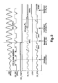
- the VCO clock of the PLL whose output signal CK_PLL is represented in FIG. 2, therefore begins to operate.
- the signal CK_PLL is used to generate the clock signal CK_CPU which will start the microcontroller. In this way, the microcontroller is started very quickly. Nevertheless, as illustrated, it is possible to provide a small delay at the oscillator VCO, which filters the first clock ticks.
- FIG. 2 illustrates the output signal of the main oscillator OSC in stabilization phase, then when it is stabilized, as well as the logical equivalent signal CK_OSC. During the stabilization phase, the presence of undesired transient pulses is noted.
- the stabilization phase of the main oscillator OSC is started while the microcontroller is awake and the user program executes using the VCO backup oscillator of the open-loop phase-locked loop as the source of the oscillator. 'clock.
- the multiplexer P can be controlled so as to provide a divided clock signal CK_CPU.
- a logic high configuration bit according to the example of FIG. 1 is loaded into the configuration register DIV16.
- the selected clock signal is the output signal of the divider circuit S.
- the selection of the clock source can be controlled via the CKSEL selection register.
- both the CSSD bit must be reset and the timer must be completed.
- the timing block of the main oscillator can count a predetermined number of cycles of the clock signal CK_OSC beyond which it is considered that the signal delivered at the output of the main oscillator is stabilized.
- the timing block of the main oscillator can deliver an OSC TEMPO logic signal in state 1 as long as the predetermined value of the counter of the delay block is not reached and passing to the logical state 0 when this value is reached, meaning that the main oscillator OSC is stabilized.
- a timer register could be provided to indicate the status of this signal.
- Switching to the main oscillator OSC to generate the clock signal CK_CPU can then be performed by loading a logic 1 according to the example, in the CKSEL selection register of the microcontroller.
- This signal can be divided or not to generate the signal CK_CPU according to the configuration of the register provided for this purpose DIV16.
- the user can therefore choose to use the PLL phase locked loop as a clock source for the microcontroller.
- a step of configuring the phase-locked loop before its activation can then be implemented, in which a configuration bit is loaded into each configuration register MX1 and MX0, making it possible to control the choice of the multiplication factor of the loop.
- the activation of the PLL phase-locked loop is controlled by the loading of a bit in the activation register PLLEN, which controls the logic gate at the input of the phase-locked loop, so as to let the stabilized signal delivered by the main oscillator pass. It is then necessary to wait for the phase locked loop to be locked before switching to the output signal CK_PLL of the loop to generate the clock signal CK_CPU of the microcontroller.
- the switching of the main oscillator OSC to the PLL phase lock loop as a clock source for generating the clock signal of the microcontroller can then be performed by loading a logic 0 according to the example, into the selection register CKSEL the microcontroller.
- This signal can be divided or not to generate the clock signal CK_CPU according to the configuration of the register provided for this purpose DIV16.
- the software configuration of the clock system is thus made very flexible for the user, who can select at any time, by loading a selection bit in the CKSEL register, a clock source among the main oscillator, the main oscillator associated with the phase-locked loop, the emergency oscillator constituted by the VCO oscillator of the phase-locked loop in open-loop mode, or an external clock.
Landscapes
- Engineering & Computer Science (AREA)
- Theoretical Computer Science (AREA)
- Physics & Mathematics (AREA)
- General Engineering & Computer Science (AREA)
- General Physics & Mathematics (AREA)
- Stabilization Of Oscillater, Synchronisation, Frequency Synthesizers (AREA)
- Microcomputers (AREA)
Applications Claiming Priority (1)
| Application Number | Priority Date | Filing Date | Title |
|---|---|---|---|
| FR0409307A FR2874766A1 (fr) | 2004-09-02 | 2004-09-02 | Procede de configuration du systeme d'horloge d'un microcontroleur |
Publications (1)
| Publication Number | Publication Date |
|---|---|
| EP1632837A1 true EP1632837A1 (de) | 2006-03-08 |
Family
ID=34949135
Family Applications (1)
| Application Number | Title | Priority Date | Filing Date |
|---|---|---|---|
| EP05291815A Ceased EP1632837A1 (de) | 2004-09-02 | 2005-08-31 | Verfahren zum Konfigurieren eines Mikrokontroller Systemtaktes |
Country Status (3)
| Country | Link |
|---|---|
| US (1) | US7581132B2 (de) |
| EP (1) | EP1632837A1 (de) |
| FR (1) | FR2874766A1 (de) |
Families Citing this family (6)
| Publication number | Priority date | Publication date | Assignee | Title |
|---|---|---|---|---|
| KR100849215B1 (ko) * | 2007-01-17 | 2008-07-31 | 삼성전자주식회사 | 전원제어장치, 방법, 및 상기 전원제어장치를 구비하는시스템 |
| US8020026B1 (en) * | 2008-02-29 | 2011-09-13 | Rf Micro Devices, Inc. | Phase-aligning corrected and uncorrected clocks |
| US8963599B2 (en) * | 2012-12-13 | 2015-02-24 | Coherent Logix, Incorporated | Multi-frequency clock skew control for inter-chip communication in synchronous digital systems |
| CN109995325B (zh) * | 2018-12-29 | 2023-05-30 | 成都锐成芯微科技股份有限公司 | 一种低噪声rc振荡器 |
| US11573594B2 (en) * | 2021-07-12 | 2023-02-07 | U-Blox Ag | Methods and apparatuses for providing a reference clock signal |
| DE102021126384A1 (de) * | 2021-10-12 | 2023-04-13 | Infineon Technologies Ag | Mikrocontroller und Verfahren zum Initialisieren eines Mikrocontrollers |
Citations (5)
| Publication number | Priority date | Publication date | Assignee | Title |
|---|---|---|---|---|
| US4893271A (en) * | 1983-11-07 | 1990-01-09 | Motorola, Inc. | Synthesized clock microcomputer with power saving |
| US5623234A (en) * | 1996-03-04 | 1997-04-22 | Motorola | Clock system |
| US6657501B1 (en) * | 2000-06-19 | 2003-12-02 | Cypress Semiconductor Corp. | Instantaneous start up oscillator |
| US20040017234A1 (en) * | 2002-07-26 | 2004-01-29 | Tam Simon M. | VCC adaptive dynamically variable frequency clock system for high performance low power microprocessors |
| US20070069829A1 (en) * | 2005-09-26 | 2007-03-29 | Cypress Semiconductor Corp. | Reducing the settling time of a crystal oscillator |
Family Cites Families (3)
| Publication number | Priority date | Publication date | Assignee | Title |
|---|---|---|---|---|
| JPH05259848A (ja) * | 1992-03-11 | 1993-10-08 | Nec Corp | クロック発生装置 |
| US5903746A (en) * | 1996-11-04 | 1999-05-11 | Texas Instruments Incorporated | Apparatus and method for automatically sequencing clocks in a data processing system when entering or leaving a low power state |
| JP2001344039A (ja) * | 2000-03-31 | 2001-12-14 | Seiko Epson Corp | 情報処理装置、情報処理装置の制御方法および情報処理装置の制御プログラム |
-
2004
- 2004-09-02 FR FR0409307A patent/FR2874766A1/fr not_active Withdrawn
-
2005
- 2005-08-31 EP EP05291815A patent/EP1632837A1/de not_active Ceased
- 2005-09-01 US US11/219,345 patent/US7581132B2/en not_active Expired - Fee Related
Patent Citations (5)
| Publication number | Priority date | Publication date | Assignee | Title |
|---|---|---|---|---|
| US4893271A (en) * | 1983-11-07 | 1990-01-09 | Motorola, Inc. | Synthesized clock microcomputer with power saving |
| US5623234A (en) * | 1996-03-04 | 1997-04-22 | Motorola | Clock system |
| US6657501B1 (en) * | 2000-06-19 | 2003-12-02 | Cypress Semiconductor Corp. | Instantaneous start up oscillator |
| US20040017234A1 (en) * | 2002-07-26 | 2004-01-29 | Tam Simon M. | VCC adaptive dynamically variable frequency clock system for high performance low power microprocessors |
| US20070069829A1 (en) * | 2005-09-26 | 2007-03-29 | Cypress Semiconductor Corp. | Reducing the settling time of a crystal oscillator |
Non-Patent Citations (1)
| Title |
|---|
| CHENG-CHAN TIEN ET AL: "An Integer-N Frequency Synthesizer Applied to MB-OFDM UWB 5th Band Group", PROGRESS IN ELECTROMAGNETICS RESEARCH SYMPOSIUM, 26 March 2007 (2007-03-26) - 30 March 2007 (2007-03-30), Beijing, pages 166 - 170 * |
Also Published As
| Publication number | Publication date |
|---|---|
| US7581132B2 (en) | 2009-08-25 |
| US20060059381A1 (en) | 2006-03-16 |
| FR2874766A1 (fr) | 2006-03-03 |
Similar Documents
| Publication | Publication Date | Title |
|---|---|---|
| EP2063328B1 (de) | Elektronischer funktionssteuerungsschaltkreis von peripheriegeräten einer uhr | |
| EP2280364B1 (de) | Fehlerinjektionsdetektor in einer integrierten Schaltung | |
| EP3044679B1 (de) | Verfahren zur aktualisierung eines startladers einer multiprozessorvorrichtung | |
| FR2689656A1 (fr) | Procédé et appareil de gestion automatique de puissance dans un dispositif hautement intégré de commande de disque souple. | |
| FR2682785A1 (fr) | Structure de microprocesseur a frequence de noyau double de celle des bus. | |
| EP4068128B1 (de) | Gesichertes starten einer verarbeitungseinheit | |
| EP1447736A1 (de) | Mikroprozessor mit energiesparenden Betriebsmodi | |
| JP3904472B2 (ja) | 1又は複数のクロック信号から出力信号を選択的に生成するための回路 | |
| WO2008009609A2 (fr) | Coeur processeur a frequence pilotee et procede de demarrage dudit coeur processeur dans un mode programme | |
| EP3171244B1 (de) | Stand-by-schaltung eines elektronischen schaltkreises | |
| FR2789501A1 (fr) | Procede et dispositif de reduction de la consommation d'un microcontroleur | |
| EP1417582B1 (de) | Schaltkreiskomplex mit dekontaminierungsmitteln für mit fehlern kontaminierte teile | |
| FR2844892A1 (fr) | Horloge de surveillance de microcontroleur | |
| FR2894693A1 (fr) | Procede et dispositif de sauvegarde et de restauration d'une maniere interruptible d'un ensemble de registres d'un microprocesseur | |
| EP0367345B1 (de) | Logikanalysator mit Doppel-Triggerung | |
| US7581132B2 (en) | System and method for configuring a microcontroller clock system | |
| FR3134462A1 (fr) | Procédé de transfert de données entre un premier domaine numérique et un deuxième domaine numérique, et système sur puce correspondant. | |
| EP1688956B1 (de) | Dynamische Speicheranordnung für ein mobiles Telefon | |
| FR2790117A1 (fr) | Procede de configuration d'un microcontroleur en mode initialisation | |
| FR2788145A1 (fr) | Procede d'initialisation d'un microcontroleur | |
| US11204778B2 (en) | Efficient hibernation apparatus and method for digital devices | |
| WO2013153167A1 (fr) | Dispositif pour générer une signature à l'exécution d'une tâche de programme et méthode de comparaison de flots d'exécution | |
| EP4145704B1 (de) | Gesichertes starten einer verarbeitungseinheit | |
| EP1102158B1 (de) | Gerät und Verfahren für die Kontrolle des Betriebszustandes eines elektronischen Systems in einem Graubereich | |
| EP2080269A1 (de) | Breitbandfrequenz-synthesizer mit eliminierung von parasitären niederfrequenzemissionen |
Legal Events
| Date | Code | Title | Description |
|---|---|---|---|
| PUAI | Public reference made under article 153(3) epc to a published international application that has entered the european phase |
Free format text: ORIGINAL CODE: 0009012 |
|
| AK | Designated contracting states |
Kind code of ref document: A1 Designated state(s): AT BE BG CH CY CZ DE DK EE ES FI FR GB GR HU IE IS IT LI LT LU LV MC NL PL PT RO SE SI SK TR |
|
| AX | Request for extension of the european patent |
Extension state: AL BA HR MK YU |
|
| 17P | Request for examination filed |
Effective date: 20060823 |
|
| AKX | Designation fees paid |
Designated state(s): DE FR GB IT |
|
| 17Q | First examination report despatched |
Effective date: 20071213 |
|
| STAA | Information on the status of an ep patent application or granted ep patent |
Free format text: STATUS: THE APPLICATION HAS BEEN REFUSED |
|
| 18R | Application refused |
Effective date: 20090515 |