EP1627412B1 - Charged particle beamlet exposure system - Google Patents
Charged particle beamlet exposure system Download PDFInfo
- Publication number
- EP1627412B1 EP1627412B1 EP04748613A EP04748613A EP1627412B1 EP 1627412 B1 EP1627412 B1 EP 1627412B1 EP 04748613 A EP04748613 A EP 04748613A EP 04748613 A EP04748613 A EP 04748613A EP 1627412 B1 EP1627412 B1 EP 1627412B1
- Authority
- EP
- European Patent Office
- Prior art keywords
- aperture
- charged particle
- beamlet
- array
- lenses
- Prior art date
- Legal status (The legal status is an assumption and is not a legal conclusion. Google has not performed a legal analysis and makes no representation as to the accuracy of the status listed.)
- Expired - Lifetime
Links
- 239000002245 particle Substances 0.000 title claims abstract description 54
- 230000000903 blocking effect Effects 0.000 claims abstract description 5
- 230000003287 optical effect Effects 0.000 claims description 26
- 238000011144 upstream manufacturing Methods 0.000 claims 1
- 238000001459 lithography Methods 0.000 description 9
- 238000003491 array Methods 0.000 description 8
- 230000000694 effects Effects 0.000 description 5
- 230000001965 increasing effect Effects 0.000 description 5
- 230000004075 alteration Effects 0.000 description 3
- 238000013459 approach Methods 0.000 description 3
- 230000003247 decreasing effect Effects 0.000 description 2
- 238000011161 development Methods 0.000 description 2
- 230000002708 enhancing effect Effects 0.000 description 2
- 230000037361 pathway Effects 0.000 description 2
- 239000004065 semiconductor Substances 0.000 description 2
- 235000012431 wafers Nutrition 0.000 description 2
- 230000000593 degrading effect Effects 0.000 description 1
- 230000001419 dependent effect Effects 0.000 description 1
- 230000005684 electric field Effects 0.000 description 1
- 230000005672 electromagnetic field Effects 0.000 description 1
- 230000005686 electrostatic field Effects 0.000 description 1
- 238000010438 heat treatment Methods 0.000 description 1
- 238000003384 imaging method Methods 0.000 description 1
- 238000000034 method Methods 0.000 description 1
- 238000002039 particle-beam lithography Methods 0.000 description 1
- 238000012545 processing Methods 0.000 description 1
- 238000007493 shaping process Methods 0.000 description 1
- 239000000758 substrate Substances 0.000 description 1
Images


Classifications
-
- H—ELECTRICITY
- H01—ELECTRIC ELEMENTS
- H01L—SEMICONDUCTOR DEVICES NOT COVERED BY CLASS H10
- H01L21/00—Processes or apparatus adapted for the manufacture or treatment of semiconductor or solid state devices or of parts thereof
- H01L21/02—Manufacture or treatment of semiconductor devices or of parts thereof
- H01L21/027—Making masks on semiconductor bodies for further photolithographic processing not provided for in group H01L21/18 or H01L21/34
- H01L21/0271—Making masks on semiconductor bodies for further photolithographic processing not provided for in group H01L21/18 or H01L21/34 comprising organic layers
- H01L21/0273—Making masks on semiconductor bodies for further photolithographic processing not provided for in group H01L21/18 or H01L21/34 comprising organic layers characterised by the treatment of photoresist layers
- H01L21/0274—Photolithographic processes
-
- H—ELECTRICITY
- H01—ELECTRIC ELEMENTS
- H01J—ELECTRIC DISCHARGE TUBES OR DISCHARGE LAMPS
- H01J37/00—Discharge tubes with provision for introducing objects or material to be exposed to the discharge, e.g. for the purpose of examination or processing thereof
- H01J37/30—Electron-beam or ion-beam tubes for localised treatment of objects
- H01J37/3002—Details
- H01J37/3007—Electron or ion-optical systems
-
- B—PERFORMING OPERATIONS; TRANSPORTING
- B82—NANOTECHNOLOGY
- B82Y—SPECIFIC USES OR APPLICATIONS OF NANOSTRUCTURES; MEASUREMENT OR ANALYSIS OF NANOSTRUCTURES; MANUFACTURE OR TREATMENT OF NANOSTRUCTURES
- B82Y10/00—Nanotechnology for information processing, storage or transmission, e.g. quantum computing or single electron logic
-
- B—PERFORMING OPERATIONS; TRANSPORTING
- B82—NANOTECHNOLOGY
- B82Y—SPECIFIC USES OR APPLICATIONS OF NANOSTRUCTURES; MEASUREMENT OR ANALYSIS OF NANOSTRUCTURES; MANUFACTURE OR TREATMENT OF NANOSTRUCTURES
- B82Y40/00—Manufacture or treatment of nanostructures
-
- H—ELECTRICITY
- H01—ELECTRIC ELEMENTS
- H01J—ELECTRIC DISCHARGE TUBES OR DISCHARGE LAMPS
- H01J37/00—Discharge tubes with provision for introducing objects or material to be exposed to the discharge, e.g. for the purpose of examination or processing thereof
- H01J37/02—Details
- H01J37/04—Arrangements of electrodes and associated parts for generating or controlling the discharge, e.g. electron-optical arrangement or ion-optical arrangement
- H01J37/045—Beam blanking or chopping, i.e. arrangements for momentarily interrupting exposure to the discharge
-
- H—ELECTRICITY
- H01—ELECTRIC ELEMENTS
- H01J—ELECTRIC DISCHARGE TUBES OR DISCHARGE LAMPS
- H01J37/00—Discharge tubes with provision for introducing objects or material to be exposed to the discharge, e.g. for the purpose of examination or processing thereof
- H01J37/30—Electron-beam or ion-beam tubes for localised treatment of objects
- H01J37/317—Electron-beam or ion-beam tubes for localised treatment of objects for changing properties of the objects or for applying thin layers thereon, e.g. for ion implantation
- H01J37/3174—Particle-beam lithography, e.g. electron beam lithography
- H01J37/3177—Multi-beam, e.g. fly's eye, comb probe
-
- H—ELECTRICITY
- H01—ELECTRIC ELEMENTS
- H01J—ELECTRIC DISCHARGE TUBES OR DISCHARGE LAMPS
- H01J2237/00—Discharge tubes exposing object to beam, e.g. for analysis treatment, etching, imaging
- H01J2237/04—Means for controlling the discharge
- H01J2237/043—Beam blanking
- H01J2237/0435—Multi-aperture
-
- H—ELECTRICITY
- H01—ELECTRIC ELEMENTS
- H01J—ELECTRIC DISCHARGE TUBES OR DISCHARGE LAMPS
- H01J2237/00—Discharge tubes exposing object to beam, e.g. for analysis treatment, etching, imaging
- H01J2237/04—Means for controlling the discharge
- H01J2237/045—Diaphragms
-
- H—ELECTRICITY
- H01—ELECTRIC ELEMENTS
- H01J—ELECTRIC DISCHARGE TUBES OR DISCHARGE LAMPS
- H01J2237/00—Discharge tubes exposing object to beam, e.g. for analysis treatment, etching, imaging
- H01J2237/04—Means for controlling the discharge
- H01J2237/045—Diaphragms
- H01J2237/0451—Diaphragms with fixed aperture
- H01J2237/0453—Diaphragms with fixed aperture multiple apertures
-
- H—ELECTRICITY
- H01—ELECTRIC ELEMENTS
- H01J—ELECTRIC DISCHARGE TUBES OR DISCHARGE LAMPS
- H01J2237/00—Discharge tubes exposing object to beam, e.g. for analysis treatment, etching, imaging
- H01J2237/04—Means for controlling the discharge
- H01J2237/049—Focusing means
- H01J2237/0492—Lens systems
-
- H—ELECTRICITY
- H01—ELECTRIC ELEMENTS
- H01J—ELECTRIC DISCHARGE TUBES OR DISCHARGE LAMPS
- H01J2237/00—Discharge tubes exposing object to beam, e.g. for analysis treatment, etching, imaging
- H01J2237/15—Means for deflecting or directing discharge
- H01J2237/1501—Beam alignment means or procedures
Definitions
- This invention relates to charged particle optical system for a charged particle exposure apparatus, in particular a maskless lithography system using charged particles.
- the supply of data can be increased in two ways.
- a first way of increasing the data rate is by sending the pattern data directly to the beam source or sources, thus switching the source of sources on and off.
- the source or sources continuously emit one or more beamlets and the pattern data is provided to modulation means that modulate the emitted beamlets along their pathway towards the target to be patterned.
- Each individual source has a settling time that is source-dependent and becomes too large easily. It is therefore preferred to modulate the beamlets along their optical pathway.
- these modulation means are often electrostatic deflection arrays, also known as blanking aperture arrays (BAA) or deflection arrays. Examples of such arrays are disclosed in US-patent 6188074 by Advantest and in EP-patent application 1253619 by Canon.
- BAA blanking aperture arrays
- deflection arrays are disclosed in US-patent 6188074 by Advantest and in EP-patent application 1253619 by Canon.
- This aperture array has several functions. In lithography systems comprising a single source it is used to split an emitted beam in a plurality of beamlets. Furthermore, it determines the opening angle of the beam at the deflection array. Additionally the aperture array reduces the heat load on the deflection array, thereby enhancing its performance.
- misalignment of the consecutive components (lenses, apertures etc.) of the system or a slight change of the position of the beam by for instance external electromagnetic fields, for instance resulting from charging of surfaces or irregularities on charged surfaces results in dose variations.
- dose variation the control of the critical dimensions of the features to be patterned is no longer guaranteed.
- One way of dealing with misalignment problems is increasing the opening angle of each beamlet, i.e. making the cross section of a beamlet on an aperture array larger than the aperture which is passes. In that way, it is ensured that the entire area of an aperture is illuminated.
- US 2002/0039829 A An example of a multi beam exposure apparatus is shown in US 2002/0039829 A.
- This apparatus comprises first and second aperture arrays and a an array of lenses arranged between these aperture arrays to adjust the focus of beams formed by the first aperture array to the second aperture array, and further beam shaping deflection units to deflect each beam independently to a desired position on the second aperture array.
- the invention therefore provides a charged particle beam exposure apparatus as defined in claim 1.
- conjugate planes planes formed by a plane on one side of a lens or lens system and its image plane at the other side of the lens or lens system by shielding or blocking.
- said lenses comprise an electrostatic lens.
- said beamlet deflectors comprise an electrostatic deflector.
- said electrostatic deflector comprises at least two deflection electrodes.
- the apparatus further comprises a second lens system arranged before said first aperture means and comprising a plurality of lenses forming an array of lenses, said lenses arranged for converging said beamlets.
- the charged particle beam exposure apparatus further comprises a third lens system arranged before said first aperture means and comprising a plurality of lenses, arranged to project images of a source of a charged particle beam exposure apparatus in the principal plane of said second lens system, the charged particle optical system further comprising a third aperture array wherein the second lens array is arranged to project images of said third aperture array on said first aperture array.
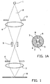
- FIGURE 1 shows cross section along the optical axis of a charged particle beam exposure apparatus comprising a charged particle source, two apertures, two lenses and one electrostatic deflector.
- the FIGURE 1A shows a top-view of FIGURE 1
- the source 1 emits a diverging charged particle beam 2.
- Said lens 4 focuses the beam substantially on the plane of the electrostatic deflector 5.
- the deflector 5 deflects the passing charged particle beam.
- the second aperture 6, being substantially round, can have several purposes. First of all it may limit the opening angle of the beam falling on the second lens 7. Secondly it blocks the beam when deflected by the electrostatic deflector 5. When the beam is transmitted through the second aperture 6 the second lens 7 focuses it on an image plane 8.
- FIGURE 2 shows the same principle of operation for a multi-beam system.
- a plurality of beamlets 9 passes consecutively a first aperture array 10, a first lens array 11, a deflector array 12, a second aperture array 13 that serves as beamlet stop array and a second lens array 14, which again focuses the transmitted beamlets 15 on an image plane 8.
- lens arrays also single lenses, arranged in one plane, can be used.
- the function of all these components is comparable with the equivalents in FIGURE 1.
- the beamlets 9 may be created with a plurality of charged particle sources or by splitting a collimated charged particle beam emitted by a single charged particle source, for instance by means of an aperture plate.
- FIGURES 1 and 2 The concept depicted in FIGURES 1 and 2 is widely used, but it has a major disadvantage that especially becomes important when operating at high deflection frequencies.
- the spot on the second aperture 6 is not sharply defined. Its intensity fades away.
- the deflection angle needed to block the beamlets 16 completely is not well defined. Consequently a large deflection angle is needed to ensure the blocking operation.
- a small deflection angle is desired.
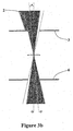
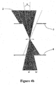
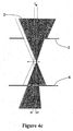
- FIGURE 3a shows an example of a correctly positioned deflector.
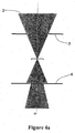
- the beamlet fills the area of both apertures.
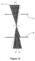
- Figure 4b shows the effect of the a slight rotation or the optical axis of beamlet 2 on the optical configuration of figure 4a: the heatload increases considerable.
- Figure 4c shows the effect of a shift in the optical axis of beamlet 2 from o to position o': again, the heat load on the second aperture increases. The heatload on the first aperture 3 also increases. Furthermore, the position of a beamlet on image plane 8 varies with the position of the optical axis of the beamlet, and with the angle of the optical axis of the beamlet.
- a simple enlargement of the opening angle has a major disadvantage though.
- the lens filling of the lens following the aperture with a larger opening angle increases. Consequently the performance of the lens deteriorates.
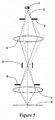
- FIGURE 5 shown a single beam optical system which does not form part of the present invention
- FIGURE 6 shows a first embodiment of the present invention for a multibeam electron optical system.
- the first aperture 3 is placed in the conjugate plane of the second aperture 6.
- the filling of the first lens 4 is therefore reduced, which enhances its performance i.e. less aberrations are introduced.
- the spot on the second aperture 6 is sharp, which results in a well-defined deflection angle of the electrostatic deflector 5 to accomplish blocking of the passing charged particle beam.
- the heat load on the first aperture 3 becomes too large, several apertures elements are arranged in a serial order along the path of the charged particle beam.
- the aperture elements are then mutually aligned and preferably arranged in a serial order with decreasing diameter along the electron optical path.
- the beam-limiting aperture element is then imaged on the second aperture 6.
- the second aperture 6 also comprises a series of aperture elements, preferably with decreasing diameter along the electron optical path, the beam limiting aperture element of the first aperture 3 is projected on the beam limiting aperture element of the second aperture 6 by the first lens 4.
- this structure is implemented in the multibeam system according to the first embodiment of the present invention as depicted in FIGURE 6.
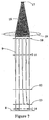
- FIGURE 7 shows such a single source multibeam electron optical system incorporated with the first embodiment of the present invention.
- a charged particle source 17 emits a diverging beam 18, which is collimated by a collimator lens 19 before reaching the first aperture array 10.
- the first aperture array 10 then splits the beam into a plurality of beamlets. The rest of the operation is similar to the operation of the system described with respect to FIGURE 6.
- the collimator lens 19 introduces additional aberrations in the system.
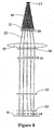
- FIGURE 8 Details of this approach are disclosed in WO 2004/081910.
- an additional lens array 20 is positioned between said collimator lens 19 and said charged particle source 17.
- a third aperture array 21 is placed between the lens array 20 and the source 17. Now the aperture array 21 splits the emitted charged particle beam 18 in a plurality of beamlets 22 and additionally takes care of the large heat load.
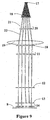
- FIGURE 9 shows the first embodiment of the present invention applied in the system depicted in FIGURE 8. Following the same reasoning as with the first embodiment regarding position variations, the position of the third aperture array 21 should be positioned in the conjugate plane of the first aperture array 10. The lens fillings of all lens arrays 11, 14, 20 are minimised, while the opening angles are large enough to deal with the position variations. Furthermore the spot on the beamlet stop array 13 remains sharp, which leads to the capability to deflect with a high frequency due to the small minimum deflection angle.
Landscapes
- Chemical & Material Sciences (AREA)
- Engineering & Computer Science (AREA)
- Analytical Chemistry (AREA)
- Nanotechnology (AREA)
- Physics & Mathematics (AREA)
- Crystallography & Structural Chemistry (AREA)
- General Physics & Mathematics (AREA)
- Manufacturing & Machinery (AREA)
- Condensed Matter Physics & Semiconductors (AREA)
- Mathematical Physics (AREA)
- Theoretical Computer Science (AREA)
- Computer Hardware Design (AREA)
- Microelectronics & Electronic Packaging (AREA)
- Power Engineering (AREA)
- Electron Beam Exposure (AREA)
- Exposure And Positioning Against Photoresist Photosensitive Materials (AREA)
Priority Applications (1)
| Application Number | Priority Date | Filing Date | Title |
|---|---|---|---|
| EP07075242A EP1830384B1 (en) | 2003-05-28 | 2004-05-27 | Charged particle beamlet exposure system |
Applications Claiming Priority (2)
| Application Number | Priority Date | Filing Date | Title |
|---|---|---|---|
| US47381003P | 2003-05-28 | 2003-05-28 | |
| PCT/NL2004/000381 WO2004107050A2 (en) | 2003-05-28 | 2004-05-27 | Charged particle beamlet exposure system |
Related Child Applications (1)
| Application Number | Title | Priority Date | Filing Date |
|---|---|---|---|
| EP07075242A Division EP1830384B1 (en) | 2003-05-28 | 2004-05-27 | Charged particle beamlet exposure system |
Publications (2)
| Publication Number | Publication Date |
|---|---|
| EP1627412A2 EP1627412A2 (en) | 2006-02-22 |
| EP1627412B1 true EP1627412B1 (en) | 2007-04-04 |
Family
ID=33490650
Family Applications (2)
| Application Number | Title | Priority Date | Filing Date |
|---|---|---|---|
| EP04748613A Expired - Lifetime EP1627412B1 (en) | 2003-05-28 | 2004-05-27 | Charged particle beamlet exposure system |
| EP07075242A Expired - Lifetime EP1830384B1 (en) | 2003-05-28 | 2004-05-27 | Charged particle beamlet exposure system |
Family Applications After (1)
| Application Number | Title | Priority Date | Filing Date |
|---|---|---|---|
| EP07075242A Expired - Lifetime EP1830384B1 (en) | 2003-05-28 | 2004-05-27 | Charged particle beamlet exposure system |
Country Status (8)
Cited By (1)
| Publication number | Priority date | Publication date | Assignee | Title |
|---|---|---|---|---|
| EP3834222A1 (en) * | 2018-08-09 | 2021-06-16 | ASML Netherlands B.V. | An apparatus for multiple charged-particle beams |
Families Citing this family (61)
| Publication number | Priority date | Publication date | Assignee | Title |
|---|---|---|---|---|
| US7462848B2 (en) * | 2003-10-07 | 2008-12-09 | Multibeam Systems, Inc. | Optics for generation of high current density patterned charged particle beams |
| US7928404B2 (en) * | 2003-10-07 | 2011-04-19 | Multibeam Corporation | Variable-ratio double-deflection beam blanker |
| US20090008579A1 (en) * | 2003-10-07 | 2009-01-08 | Tokyo Electron Limited | Electron beam lithography apparatus and design method of patterned beam-defining aperture |
| KR101099487B1 (ko) * | 2004-05-17 | 2011-12-28 | 마퍼 리쏘그라피 아이피 비.브이. | 대전 입자 빔 노광 시스템 |
| US7425713B2 (en) * | 2005-01-14 | 2008-09-16 | Arradiance, Inc. | Synchronous raster scanning lithographic system |
| NL1029132C2 (nl) * | 2005-05-26 | 2006-11-28 | Univ Delft Tech | Inrichting voor het opwekken van evenwijdige stralenbundeldelen. |
| US8597089B2 (en) * | 2005-07-08 | 2013-12-03 | Praxair Technology, Inc. | System and method for treating live cargo such as poultry with gas |
| EP1941528B9 (en) * | 2005-09-06 | 2011-09-28 | Carl Zeiss SMT GmbH | Particle-optical arrangement with particle-optical component |
| CN101443877A (zh) * | 2006-03-27 | 2009-05-27 | 多束系统公司 | 用于生成高电流密度构图带电粒子束的光学器件 |
| DE602007003089D1 (de) * | 2006-04-03 | 2009-12-17 | Ims Nanofabrication Ag | Teilchenstrahl-belichtungsvorrichtung mit gesamtmo |
| US8134135B2 (en) * | 2006-07-25 | 2012-03-13 | Mapper Lithography Ip B.V. | Multiple beam charged particle optical system |
| US7569834B1 (en) | 2006-10-18 | 2009-08-04 | Kla-Tencor Technologies Corporation | High resolution charged particle projection lens array using magnetic elements |
| EP2019415B1 (en) * | 2007-07-24 | 2016-05-11 | IMS Nanofabrication AG | Multi-beam source |
| US8890094B2 (en) | 2008-02-26 | 2014-11-18 | Mapper Lithography Ip B.V. | Projection lens arrangement |
| US8445869B2 (en) | 2008-04-15 | 2013-05-21 | Mapper Lithography Ip B.V. | Projection lens arrangement |
| CN102067272B (zh) | 2008-04-15 | 2014-04-30 | 迈普尔平版印刷Ip有限公司 | 投影透镜装置 |
| US7851774B2 (en) * | 2008-04-25 | 2010-12-14 | Taiwan Semiconductor Manufacturing Company, Ltd. | System and method for direct writing to a wafer |
| WO2009141428A1 (en) * | 2008-05-23 | 2009-11-26 | Mapper Lithography Ip B.V. | Imaging system |
| EP2128885A1 (en) * | 2008-05-26 | 2009-12-02 | FEI Company | Charged particle source with integrated energy filter |
| WO2010094801A1 (en) | 2009-02-22 | 2010-08-26 | Mapper Lithography Ip B.V. | A method and arrangement for realizing a vacuum in a vacuum chamber |
| EP2399273B1 (en) | 2009-02-22 | 2017-06-28 | Mapper Lithography IP B.V. | Charged particle lithography apparatus and method of generating vacuum in a vacuum chamber |
| US20110049393A1 (en) | 2009-02-22 | 2011-03-03 | Mapper Lithography Ip B.V. | Lithography Machine and Substrate Handling Arrangement |
| EP2399270B1 (en) * | 2009-02-22 | 2013-06-12 | Mapper Lithography IP B.V. | Charged particle lithography apparatus |
| JP5801289B2 (ja) | 2009-05-20 | 2015-10-28 | マッパー・リソグラフィー・アイピー・ビー.ブイ. | リソグラフシステムのためのパターンデータ変換 |
| JP5801288B2 (ja) * | 2009-05-20 | 2015-10-28 | マッパー・リソグラフィー・アイピー・ビー.ブイ. | リソグラフ処理のための2レベルパターンを発生する方法およびその方法を使用するパターン発生器 |
| KR101854828B1 (ko) | 2009-05-20 | 2018-05-04 | 마퍼 리쏘그라피 아이피 비.브이. | 듀얼 패스 스캐닝 |
| NL2005584C2 (en) | 2009-10-26 | 2014-09-04 | Mapper Lithography Ip Bv | Charged particle multi-beamlet lithography system with modulation device. |
| US8952342B2 (en) * | 2009-12-17 | 2015-02-10 | Mapper Lithography Ip B.V. | Support and positioning structure, semiconductor equipment system and method for positioning |
| JP6092111B2 (ja) * | 2010-10-26 | 2017-03-08 | マッパー・リソグラフィー・アイピー・ビー.ブイ. | リソグラフィシステム、変調装置およびファイバ固定基板を製造する方法 |
| WO2012062932A1 (en) | 2010-11-13 | 2012-05-18 | Mapper Lithography Ip B.V. | Charged particle lithography system with intermediate chamber |
| US8884255B2 (en) | 2010-11-13 | 2014-11-11 | Mapper Lithography Ip B.V. | Data path for lithography apparatus |
| US9305747B2 (en) | 2010-11-13 | 2016-04-05 | Mapper Lithography Ip B.V. | Data path for lithography apparatus |
| EP2638559B1 (en) | 2010-11-13 | 2016-07-20 | Mapper Lithography IP B.V. | Charged particle beam modulator |
| WO2012065941A1 (en) | 2010-11-13 | 2012-05-24 | Mapper Lithography Ip B.V. | Charged particle lithography system with aperture array cooling |
| CN103370655B (zh) | 2010-12-14 | 2016-03-16 | 迈普尔平版印刷Ip有限公司 | 光刻系统和在该光刻系统中处理基板的方法 |
| WO2012110465A2 (en) | 2011-02-16 | 2012-08-23 | Mapper Lithography Ip B.V. | System for magnetic shielding |
| KR101791252B1 (ko) | 2011-04-22 | 2017-10-27 | 마퍼 리쏘그라피 아이피 비.브이. | 리소그래피 머신들의 클러스터를 위한 네트워크 아키텍처 및 프로토콜 |
| TWI486723B (zh) | 2011-04-28 | 2015-06-01 | Mapper Lithography Ip Bv | 在微影系統中處理基板的方法 |
| RU2014114517A (ru) * | 2011-09-12 | 2015-10-20 | МЭППЕР ЛИТОГРАФИ АйПи Б.В. | Устройство обработки подложки |
| US9224580B2 (en) | 2011-09-28 | 2015-12-29 | Mapper Litohgraphy Ip B.V. | Plasma generator |
| USRE49732E1 (en) * | 2012-03-08 | 2023-11-21 | Asml Netherlands B.V. | Charged particle lithography system with alignment sensor and beam measurement sensor |
| KR102136829B1 (ko) | 2012-03-20 | 2020-07-24 | 에이에스엠엘 네델란즈 비.브이. | 라디칼을 운반하기 위한 배열체 및 방법 |
| TW201401330A (zh) | 2012-05-14 | 2014-01-01 | Mapper Lithography Ip Bv | 帶電粒子微影系統和射束產生器 |
| US10586625B2 (en) | 2012-05-14 | 2020-03-10 | Asml Netherlands B.V. | Vacuum chamber arrangement for charged particle beam generator |
| NL2010759C2 (en) | 2012-05-14 | 2015-08-25 | Mapper Lithography Ip Bv | Modulation device and power supply arrangement. |
| US11348756B2 (en) | 2012-05-14 | 2022-05-31 | Asml Netherlands B.V. | Aberration correction in charged particle system |
| KR101945964B1 (ko) | 2012-05-14 | 2019-02-11 | 마퍼 리쏘그라피 아이피 비.브이. | 하전 입자 다중-빔렛 리소그래피 시스템 및 냉각 장치 제조 방법 |
| NL2010760C2 (en) | 2013-05-03 | 2014-11-04 | Mapper Lithography Ip Bv | Beam grid layout. |
| EP2816585A1 (en) * | 2013-06-17 | 2014-12-24 | ICT Integrated Circuit Testing Gesellschaft für Halbleiterprüftechnik mbH | Charged particle beam system and method of operating thereof |
| WO2015024956A1 (en) | 2013-08-23 | 2015-02-26 | Mapper Lithography Ip B.V. | Drying device for use in a lithography system |
| CN105874560B (zh) | 2013-11-14 | 2018-07-20 | 迈普尔平版印刷Ip有限公司 | 电极堆栈布置 |
| NL2014029B1 (en) | 2013-12-30 | 2016-01-08 | Mapper Lithography Ip Bv | Cathode arrangement, electron gun, and lithography system comprising such electron gun. |
| EP3218926A2 (en) | 2014-11-14 | 2017-09-20 | Mapper Lithography IP B.V. | Load lock system and method for transferring substrates in a lithography system |
| US9484188B2 (en) | 2015-03-11 | 2016-11-01 | Mapper Lithography Ip B.V. | Individual beam pattern placement verification in multiple beam lithography |
| US10096450B2 (en) | 2015-12-28 | 2018-10-09 | Mapper Lithography Ip B.V. | Control system and method for lithography apparatus |
| US9981293B2 (en) | 2016-04-21 | 2018-05-29 | Mapper Lithography Ip B.V. | Method and system for the removal and/or avoidance of contamination in charged particle beam systems |
| KR102401179B1 (ko) * | 2017-12-12 | 2022-05-24 | 삼성전자주식회사 | 전자빔 장치의 어퍼처 시스템, 전자빔 노광 장치 및 전자빔 노광 장치 시스템 |
| CN111971774B (zh) * | 2018-03-29 | 2023-09-29 | 株式会社日立高新技术 | 带电粒子束装置 |
| NL2022156B1 (en) | 2018-12-10 | 2020-07-02 | Asml Netherlands Bv | Plasma source control circuit |
| WO2020141041A1 (en) * | 2018-12-31 | 2020-07-09 | Asml Netherlands B.V. | Systems and methods for real time stereo imaging using multiple electron beams |
| US11651934B2 (en) | 2021-09-30 | 2023-05-16 | Kla Corporation | Systems and methods of creating multiple electron beams |
Family Cites Families (15)
| Publication number | Priority date | Publication date | Assignee | Title |
|---|---|---|---|---|
| US4243866A (en) * | 1979-01-11 | 1981-01-06 | International Business Machines Corporation | Method and apparatus for forming a variable size electron beam |
| DE3172441D1 (en) | 1980-10-15 | 1985-10-31 | Toshiba Kk | Electron beam exposure system |
| US4544847A (en) * | 1983-07-28 | 1985-10-01 | Varian Associates, Inc. | Multi-gap magnetic imaging lens for charged particle beams |
| JPS6142132A (ja) * | 1984-08-06 | 1986-02-28 | Nippon Telegr & Teleph Corp <Ntt> | 荷電ビ−ム露光装置 |
| JPH097538A (ja) * | 1995-06-26 | 1997-01-10 | Nippon Telegr & Teleph Corp <Ntt> | 荷電ビーム描画装置 |
| JP3908294B2 (ja) * | 1996-02-02 | 2007-04-25 | 富士通株式会社 | 電子ビームの電流量を削減する電子ビーム露光装置及び電子ビーム露光方法 |
| US5912469A (en) * | 1996-07-11 | 1999-06-15 | Nikon Corporation | Charged-particle-beam microlithography apparatus |
| KR19990062942A (ko) | 1997-12-10 | 1999-07-26 | 히로시 오우라 | 전하 입자 빔 노출 장치 |
| US6014200A (en) * | 1998-02-24 | 2000-01-11 | Nikon Corporation | High throughput electron beam lithography system |
| JP4578606B2 (ja) * | 2000-02-09 | 2010-11-10 | 富士通セミコンダクター株式会社 | 荷電粒子ビーム描画装置及び荷電粒子ビームサイズの調整方法 |
| US6651513B2 (en) | 2000-04-27 | 2003-11-25 | Endress + Hauser Flowtec Ag | Vibration meter and method of measuring a viscosity of a fluid |
| JP4112791B2 (ja) * | 2000-10-03 | 2008-07-02 | 株式会社アドバンテスト | 電子ビーム補正方法及び電子ビーム露光装置 |
| JP4601146B2 (ja) | 2000-10-03 | 2010-12-22 | 株式会社アドバンテスト | 電子ビーム露光装置 |
| JP2002217089A (ja) * | 2001-01-18 | 2002-08-02 | Advantest Corp | 電子ビーム偏向装置、電子ビーム偏向装置の製造方法、及び電子ビーム露光装置 |
| JP4647820B2 (ja) * | 2001-04-23 | 2011-03-09 | キヤノン株式会社 | 荷電粒子線描画装置、および、デバイスの製造方法 |
-
2004
- 2004-05-27 AT AT07075242T patent/ATE524822T1/de active
- 2004-05-27 US US10/856,050 patent/US7084414B2/en not_active Expired - Fee Related
- 2004-05-27 CN CNB2004800145787A patent/CN100543920C/zh not_active Expired - Lifetime
- 2004-05-27 KR KR1020057022719A patent/KR101168200B1/ko not_active Expired - Lifetime
- 2004-05-27 JP JP2006532135A patent/JP4949843B2/ja not_active Expired - Fee Related
- 2004-05-27 KR KR1020127003554A patent/KR101175523B1/ko not_active Expired - Lifetime
- 2004-05-27 WO PCT/NL2004/000381 patent/WO2004107050A2/en active IP Right Grant
- 2004-05-27 EP EP04748613A patent/EP1627412B1/en not_active Expired - Lifetime
- 2004-05-27 EP EP07075242A patent/EP1830384B1/en not_active Expired - Lifetime
- 2004-05-27 AT AT04748613T patent/ATE358885T1/de active
- 2004-05-27 DE DE602004005704T patent/DE602004005704T2/de not_active Expired - Lifetime
Cited By (2)
| Publication number | Priority date | Publication date | Assignee | Title |
|---|---|---|---|---|
| EP3834222A1 (en) * | 2018-08-09 | 2021-06-16 | ASML Netherlands B.V. | An apparatus for multiple charged-particle beams |
| US12080515B2 (en) | 2018-08-09 | 2024-09-03 | Asml Netherlands B.V. | Apparatus for multiple charged-particle beams |
Also Published As
| Publication number | Publication date |
|---|---|
| DE602004005704T2 (de) | 2007-12-27 |
| WO2004107050A2 (en) | 2004-12-09 |
| EP1830384A2 (en) | 2007-09-05 |
| ATE358885T1 (de) | 2007-04-15 |
| DE602004005704D1 (de) | 2007-05-16 |
| CN1795529A (zh) | 2006-06-28 |
| WO2004107050A3 (en) | 2005-04-21 |
| CN100543920C (zh) | 2009-09-23 |
| US7084414B2 (en) | 2006-08-01 |
| US20050161621A1 (en) | 2005-07-28 |
| JP2007500948A (ja) | 2007-01-18 |
| EP1830384A3 (en) | 2007-09-19 |
| JP4949843B2 (ja) | 2012-06-13 |
| EP1830384B1 (en) | 2011-09-14 |
| KR101168200B1 (ko) | 2012-07-25 |
| KR20120025629A (ko) | 2012-03-15 |
| KR20060036391A (ko) | 2006-04-28 |
| EP1627412A2 (en) | 2006-02-22 |
| KR101175523B1 (ko) | 2012-08-21 |
| ATE524822T1 (de) | 2011-09-15 |
Similar Documents
| Publication | Publication Date | Title |
|---|---|---|
| EP1627412B1 (en) | Charged particle beamlet exposure system | |
| TWI534849B (zh) | 投影透鏡配置 | |
| JP4995261B2 (ja) | パターン化ビームの総合変調を持つ粒子ビーム露光装置 | |
| US5831270A (en) | Magnetic deflectors and charged-particle-beam lithography systems incorporating same | |
| EP3020062B1 (en) | Beam grid layout | |
| EP1602121B1 (en) | Apparatus for generating a plurality of beamlets | |
| KR101900050B1 (ko) | 멀티 하전 입자빔 장치 | |
| KR20110030466A (ko) | 이미징 시스템 | |
| WO1999047978A1 (en) | Method and apparatus for direct writing of semiconductor die using microcolumn array | |
| KR102468349B1 (ko) | 멀티 빔용 애퍼처 기판 세트 및 멀티 하전 입자 빔 장치 | |
| JP4843679B2 (ja) | 荷電粒子ビーム曝露システム | |
| KR102025602B1 (ko) | 멀티 빔용 애퍼쳐 세트 및 멀티 하전 입자 빔 묘화 장치 | |
| JP3800343B2 (ja) | 荷電粒子ビーム露光装置 | |
| JP3983772B2 (ja) | 荷電粒子ビーム応用装置 | |
| JP2019079953A (ja) | マルチ荷電粒子ビーム描画装置 | |
| JP2005203464A (ja) | 荷電粒子ビーム露光装置 | |
| WO2002103764A1 (fr) | Systeme d'exposition par faisceau d'electrons |
Legal Events
| Date | Code | Title | Description |
|---|---|---|---|
| PUAI | Public reference made under article 153(3) epc to a published international application that has entered the european phase |
Free format text: ORIGINAL CODE: 0009012 |
|
| 17P | Request for examination filed |
Effective date: 20051125 |
|
| AK | Designated contracting states |
Kind code of ref document: A2 Designated state(s): AT BE BG CH CY CZ DE DK EE ES FI FR GB GR HU IE IT LI LU MC NL PL PT RO SE SI SK TR |
|
| DAX | Request for extension of the european patent (deleted) | ||
| GRAP | Despatch of communication of intention to grant a patent |
Free format text: ORIGINAL CODE: EPIDOSNIGR1 |
|
| GRAS | Grant fee paid |
Free format text: ORIGINAL CODE: EPIDOSNIGR3 |
|
| GRAA | (expected) grant |
Free format text: ORIGINAL CODE: 0009210 |
|
| AK | Designated contracting states |
Kind code of ref document: B1 Designated state(s): AT BE BG CH CY CZ DE DK EE ES FI FR GB GR HU IE IT LI LU MC NL PL PT RO SE SI SK TR |
|
| PG25 | Lapsed in a contracting state [announced via postgrant information from national office to epo] |
Ref country code: LI Free format text: LAPSE BECAUSE OF FAILURE TO SUBMIT A TRANSLATION OF THE DESCRIPTION OR TO PAY THE FEE WITHIN THE PRESCRIBED TIME-LIMIT Effective date: 20070404 Ref country code: FI Free format text: LAPSE BECAUSE OF FAILURE TO SUBMIT A TRANSLATION OF THE DESCRIPTION OR TO PAY THE FEE WITHIN THE PRESCRIBED TIME-LIMIT Effective date: 20070404 Ref country code: SI Free format text: LAPSE BECAUSE OF FAILURE TO SUBMIT A TRANSLATION OF THE DESCRIPTION OR TO PAY THE FEE WITHIN THE PRESCRIBED TIME-LIMIT Effective date: 20070404 Ref country code: CH Free format text: LAPSE BECAUSE OF FAILURE TO SUBMIT A TRANSLATION OF THE DESCRIPTION OR TO PAY THE FEE WITHIN THE PRESCRIBED TIME-LIMIT Effective date: 20070404 |
|
| REG | Reference to a national code |
Ref country code: GB Ref legal event code: FG4D |
|
| REG | Reference to a national code |
Ref country code: CH Ref legal event code: EP |
|
| REF | Corresponds to: |
Ref document number: 602004005704 Country of ref document: DE Date of ref document: 20070516 Kind code of ref document: P |
|
| REG | Reference to a national code |
Ref country code: IE Ref legal event code: FG4D |
|
| PG25 | Lapsed in a contracting state [announced via postgrant information from national office to epo] |
Ref country code: ES Free format text: LAPSE BECAUSE OF FAILURE TO SUBMIT A TRANSLATION OF THE DESCRIPTION OR TO PAY THE FEE WITHIN THE PRESCRIBED TIME-LIMIT Effective date: 20070715 |
|
| REG | Reference to a national code |
Ref country code: SE Ref legal event code: TRGR |
|
| PG25 | Lapsed in a contracting state [announced via postgrant information from national office to epo] |
Ref country code: PT Free format text: LAPSE BECAUSE OF FAILURE TO SUBMIT A TRANSLATION OF THE DESCRIPTION OR TO PAY THE FEE WITHIN THE PRESCRIBED TIME-LIMIT Effective date: 20070904 |
|
| ET | Fr: translation filed | ||
| REG | Reference to a national code |
Ref country code: CH Ref legal event code: PL |
|
| PG25 | Lapsed in a contracting state [announced via postgrant information from national office to epo] |
Ref country code: PL Free format text: LAPSE BECAUSE OF FAILURE TO SUBMIT A TRANSLATION OF THE DESCRIPTION OR TO PAY THE FEE WITHIN THE PRESCRIBED TIME-LIMIT Effective date: 20070404 |
|
| PG25 | Lapsed in a contracting state [announced via postgrant information from national office to epo] |
Ref country code: BG Free format text: LAPSE BECAUSE OF FAILURE TO SUBMIT A TRANSLATION OF THE DESCRIPTION OR TO PAY THE FEE WITHIN THE PRESCRIBED TIME-LIMIT Effective date: 20070704 Ref country code: DK Free format text: LAPSE BECAUSE OF FAILURE TO SUBMIT A TRANSLATION OF THE DESCRIPTION OR TO PAY THE FEE WITHIN THE PRESCRIBED TIME-LIMIT Effective date: 20070404 Ref country code: MC Free format text: LAPSE BECAUSE OF NON-PAYMENT OF DUE FEES Effective date: 20070531 Ref country code: CZ Free format text: LAPSE BECAUSE OF FAILURE TO SUBMIT A TRANSLATION OF THE DESCRIPTION OR TO PAY THE FEE WITHIN THE PRESCRIBED TIME-LIMIT Effective date: 20070404 |
|
| PLBE | No opposition filed within time limit |
Free format text: ORIGINAL CODE: 0009261 |
|
| STAA | Information on the status of an ep patent application or granted ep patent |
Free format text: STATUS: NO OPPOSITION FILED WITHIN TIME LIMIT |
|
| PG25 | Lapsed in a contracting state [announced via postgrant information from national office to epo] |
Ref country code: SK Free format text: LAPSE BECAUSE OF FAILURE TO SUBMIT A TRANSLATION OF THE DESCRIPTION OR TO PAY THE FEE WITHIN THE PRESCRIBED TIME-LIMIT Effective date: 20070404 |
|
| 26N | No opposition filed |
Effective date: 20080107 |
|
| PG25 | Lapsed in a contracting state [announced via postgrant information from national office to epo] |
Ref country code: GR Free format text: LAPSE BECAUSE OF FAILURE TO SUBMIT A TRANSLATION OF THE DESCRIPTION OR TO PAY THE FEE WITHIN THE PRESCRIBED TIME-LIMIT Effective date: 20070705 |
|
| PG25 | Lapsed in a contracting state [announced via postgrant information from national office to epo] |
Ref country code: RO Free format text: LAPSE BECAUSE OF FAILURE TO SUBMIT A TRANSLATION OF THE DESCRIPTION OR TO PAY THE FEE WITHIN THE PRESCRIBED TIME-LIMIT Effective date: 20070404 |
|
| PG25 | Lapsed in a contracting state [announced via postgrant information from national office to epo] |
Ref country code: EE Free format text: LAPSE BECAUSE OF FAILURE TO SUBMIT A TRANSLATION OF THE DESCRIPTION OR TO PAY THE FEE WITHIN THE PRESCRIBED TIME-LIMIT Effective date: 20070404 |
|
| PG25 | Lapsed in a contracting state [announced via postgrant information from national office to epo] |
Ref country code: CY Free format text: LAPSE BECAUSE OF FAILURE TO SUBMIT A TRANSLATION OF THE DESCRIPTION OR TO PAY THE FEE WITHIN THE PRESCRIBED TIME-LIMIT Effective date: 20070404 |
|
| PG25 | Lapsed in a contracting state [announced via postgrant information from national office to epo] |
Ref country code: LU Free format text: LAPSE BECAUSE OF NON-PAYMENT OF DUE FEES Effective date: 20070527 |
|
| PG25 | Lapsed in a contracting state [announced via postgrant information from national office to epo] |
Ref country code: TR Free format text: LAPSE BECAUSE OF FAILURE TO SUBMIT A TRANSLATION OF THE DESCRIPTION OR TO PAY THE FEE WITHIN THE PRESCRIBED TIME-LIMIT Effective date: 20070404 Ref country code: HU Free format text: LAPSE BECAUSE OF FAILURE TO SUBMIT A TRANSLATION OF THE DESCRIPTION OR TO PAY THE FEE WITHIN THE PRESCRIBED TIME-LIMIT Effective date: 20071005 |
|
| PGFP | Annual fee paid to national office [announced via postgrant information from national office to epo] |
Ref country code: GB Payment date: 20140519 Year of fee payment: 11 |
|
| PGFP | Annual fee paid to national office [announced via postgrant information from national office to epo] |
Ref country code: IT Payment date: 20140526 Year of fee payment: 11 Ref country code: SE Payment date: 20140513 Year of fee payment: 11 |
|
| PGFP | Annual fee paid to national office [announced via postgrant information from national office to epo] |
Ref country code: BE Payment date: 20140513 Year of fee payment: 11 |
|
| GBPC | Gb: european patent ceased through non-payment of renewal fee |
Effective date: 20150527 |
|
| PG25 | Lapsed in a contracting state [announced via postgrant information from national office to epo] |
Ref country code: IT Free format text: LAPSE BECAUSE OF NON-PAYMENT OF DUE FEES Effective date: 20150527 |
|
| PG25 | Lapsed in a contracting state [announced via postgrant information from national office to epo] |
Ref country code: SE Free format text: LAPSE BECAUSE OF NON-PAYMENT OF DUE FEES Effective date: 20150528 |
|
| PG25 | Lapsed in a contracting state [announced via postgrant information from national office to epo] |
Ref country code: GB Free format text: LAPSE BECAUSE OF NON-PAYMENT OF DUE FEES Effective date: 20150527 |
|
| REG | Reference to a national code |
Ref country code: FR Ref legal event code: PLFP Year of fee payment: 13 |
|
| REG | Reference to a national code |
Ref country code: FR Ref legal event code: PLFP Year of fee payment: 14 |
|
| PG25 | Lapsed in a contracting state [announced via postgrant information from national office to epo] |
Ref country code: BE Free format text: LAPSE BECAUSE OF NON-PAYMENT OF DUE FEES Effective date: 20150531 |
|
| REG | Reference to a national code |
Ref country code: FR Ref legal event code: PLFP Year of fee payment: 15 |
|
| REG | Reference to a national code |
Ref country code: NL Ref legal event code: QB Free format text: DETAILS LICENCE OR PLEDGE: LICENCE, NEW LICENCE REGISTRATION Name of requester: DELFT UNIVERSITY OF TECHNOLOGY Effective date: 20190110 |
|
| REG | Reference to a national code |
Ref country code: NL Ref legal event code: PD Owner name: ASML NETHERLANDS B.V.; NL Free format text: DETAILS ASSIGNMENT: CHANGE OF OWNER(S), ASSIGNMENT; FORMER OWNER NAME: MAPPER LITHOGRAPHY B.V. Effective date: 20190425 |
|
| PGFP | Annual fee paid to national office [announced via postgrant information from national office to epo] |
Ref country code: IE Payment date: 20220518 Year of fee payment: 19 Ref country code: FR Payment date: 20220526 Year of fee payment: 19 Ref country code: DE Payment date: 20220527 Year of fee payment: 19 |
|
| PGFP | Annual fee paid to national office [announced via postgrant information from national office to epo] |
Ref country code: AT Payment date: 20220518 Year of fee payment: 19 |
|
| P01 | Opt-out of the competence of the unified patent court (upc) registered |
Effective date: 20230403 |
|
| PGFP | Annual fee paid to national office [announced via postgrant information from national office to epo] |
Ref country code: NL Payment date: 20230525 Year of fee payment: 20 |
|
| REG | Reference to a national code |
Ref country code: DE Ref legal event code: R119 Ref document number: 602004005704 Country of ref document: DE |
|
| REG | Reference to a national code |
Ref country code: AT Ref legal event code: MM01 Ref document number: 358885 Country of ref document: AT Kind code of ref document: T Effective date: 20230527 |
|
| PG25 | Lapsed in a contracting state [announced via postgrant information from national office to epo] |
Ref country code: AT Free format text: LAPSE BECAUSE OF NON-PAYMENT OF DUE FEES Effective date: 20230527 |
|
| REG | Reference to a national code |
Ref country code: IE Ref legal event code: MM4A |
|
| PG25 | Lapsed in a contracting state [announced via postgrant information from national office to epo] |
Ref country code: IE Free format text: LAPSE BECAUSE OF NON-PAYMENT OF DUE FEES Effective date: 20230527 |
|
| PG25 | Lapsed in a contracting state [announced via postgrant information from national office to epo] |
Ref country code: IE Free format text: LAPSE BECAUSE OF NON-PAYMENT OF DUE FEES Effective date: 20230527 Ref country code: DE Free format text: LAPSE BECAUSE OF NON-PAYMENT OF DUE FEES Effective date: 20231201 |
|
| REG | Reference to a national code |
Ref country code: NL Ref legal event code: MK Effective date: 20240526 |
|
| PG25 | Lapsed in a contracting state [announced via postgrant information from national office to epo] |
Ref country code: FR Free format text: LAPSE BECAUSE OF NON-PAYMENT OF DUE FEES Effective date: 20230531 |