EP1619788A1 - Oscillateur contrôlé en tension à capacité linéaire - Google Patents
Oscillateur contrôlé en tension à capacité linéaire Download PDFInfo
- Publication number
- EP1619788A1 EP1619788A1 EP05354024A EP05354024A EP1619788A1 EP 1619788 A1 EP1619788 A1 EP 1619788A1 EP 05354024 A EP05354024 A EP 05354024A EP 05354024 A EP05354024 A EP 05354024A EP 1619788 A1 EP1619788 A1 EP 1619788A1
- Authority
- EP
- European Patent Office
- Prior art keywords
- capacitance
- variable capacitors
- control voltage
- voltage
- variable
- Prior art date
- Legal status (The legal status is an assumption and is not a legal conclusion. Google has not performed a legal analysis and makes no representation as to the accuracy of the status listed.)
- Granted
Links
Images
Classifications
-
- H—ELECTRICITY
- H03—ELECTRONIC CIRCUITRY
- H03B—GENERATION OF OSCILLATIONS, DIRECTLY OR BY FREQUENCY-CHANGING, BY CIRCUITS EMPLOYING ACTIVE ELEMENTS WHICH OPERATE IN A NON-SWITCHING MANNER; GENERATION OF NOISE BY SUCH CIRCUITS
- H03B5/00—Generation of oscillations using amplifier with regenerative feedback from output to input
- H03B5/08—Generation of oscillations using amplifier with regenerative feedback from output to input with frequency-determining element comprising lumped inductance and capacitance
- H03B5/12—Generation of oscillations using amplifier with regenerative feedback from output to input with frequency-determining element comprising lumped inductance and capacitance active element in amplifier being semiconductor device
- H03B5/1296—Generation of oscillations using amplifier with regenerative feedback from output to input with frequency-determining element comprising lumped inductance and capacitance active element in amplifier being semiconductor device the feedback circuit comprising a transformer
-
- H—ELECTRICITY
- H03—ELECTRONIC CIRCUITRY
- H03B—GENERATION OF OSCILLATIONS, DIRECTLY OR BY FREQUENCY-CHANGING, BY CIRCUITS EMPLOYING ACTIVE ELEMENTS WHICH OPERATE IN A NON-SWITCHING MANNER; GENERATION OF NOISE BY SUCH CIRCUITS
- H03B5/00—Generation of oscillations using amplifier with regenerative feedback from output to input
- H03B5/08—Generation of oscillations using amplifier with regenerative feedback from output to input with frequency-determining element comprising lumped inductance and capacitance
- H03B5/12—Generation of oscillations using amplifier with regenerative feedback from output to input with frequency-determining element comprising lumped inductance and capacitance active element in amplifier being semiconductor device
- H03B5/1206—Generation of oscillations using amplifier with regenerative feedback from output to input with frequency-determining element comprising lumped inductance and capacitance active element in amplifier being semiconductor device using multiple transistors for amplification
-
- H—ELECTRICITY
- H03—ELECTRONIC CIRCUITRY
- H03B—GENERATION OF OSCILLATIONS, DIRECTLY OR BY FREQUENCY-CHANGING, BY CIRCUITS EMPLOYING ACTIVE ELEMENTS WHICH OPERATE IN A NON-SWITCHING MANNER; GENERATION OF NOISE BY SUCH CIRCUITS
- H03B5/00—Generation of oscillations using amplifier with regenerative feedback from output to input
- H03B5/08—Generation of oscillations using amplifier with regenerative feedback from output to input with frequency-determining element comprising lumped inductance and capacitance
- H03B5/12—Generation of oscillations using amplifier with regenerative feedback from output to input with frequency-determining element comprising lumped inductance and capacitance active element in amplifier being semiconductor device
- H03B5/1237—Generation of oscillations using amplifier with regenerative feedback from output to input with frequency-determining element comprising lumped inductance and capacitance active element in amplifier being semiconductor device comprising means for varying the frequency of the generator
- H03B5/124—Generation of oscillations using amplifier with regenerative feedback from output to input with frequency-determining element comprising lumped inductance and capacitance active element in amplifier being semiconductor device comprising means for varying the frequency of the generator the means comprising a voltage dependent capacitance
Definitions
- the invention relates to a voltage controlled oscillator comprising an amplifier and an oscillating network comprising an inductor and at least first and second variable capacitors each having a capacitance varying according to its control voltage.
- a Voltage Controlled Oscillator provides oscillating signals whose frequency varies with a control voltage Uc.
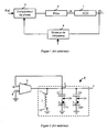
- the voltage-controlled oscillators are often used in phase-locked loops, as shown in FIG. 1.
- a loop conventionally comprises a voltage-controlled oscillator 1, the input of which is connected, via a filter. 2, at the output of a phase comparator 3 and whose output, which constitutes the output of the loop, is connected to a first input of the phase comparator 3, possibly via a frequency divider 4.
- Clock signals having a predetermined frequency Fref reference and for example provided by a crystal oscillator, are applied to a second input of the phase comparator 3.
- the control voltage Uc of the oscillator is thus a function of the difference between the frequency Fs of the output signals of the oscillator 1, possibly affected by a division coefficient, and the reference frequency Fref.
- the output frequency Fs is thus equal to the reference frequency Fref or to a multiple of it.
- phase locked loop is used in many circuits requiring frequency synthesis, especially in the radio frequency domain, for receiving modulated signals.
- Several transmission standards for example standard GSM, GPS or DCS, standards using Bluetooth technology or a wireless local area network (WLAN), are often used in the same receiver, especially in mobile phones. It is then desirable to be able to switch quickly from one standard to another, for example from a GSM type standard to a Bluetooth type standard.
- a voltage controlled oscillator typically comprises an amplifier and an LC type oscillating network.
- the oscillating network is very important because its design depends on the performance of the circuit, for example the phase noise, the quality coefficient, the oscillation frequency, etc.
- the total capacitance Ct and the oscillation frequency F vary non-linearly with the control voltage.
- a first technique consists in using a variable capacitor in a restricted range of the control voltage Uc, in which the capacitance varies linearly.
- Uc control voltage
- This technique makes it possible to obtain a linear capacitance / voltage characteristic but the gain of the oscillator is, in this case, very large and the phase noise is thus important.
- the voltage range is reduced, the servocontrol of a phase-locked loop is more difficult to achieve and a stability of the loop is difficult to achieve.
- a second technique consists in biasing differently variable capacitors connected in parallel. This technique makes it possible to obtain a linear capacitance / voltage characteristic. However, this technique is difficult to achieve.
- US Pat. No. 6,396,356 describes a voltage controlled oscillator 1 comprising a plurality of variable capacitors whose linear parts of capacitance / voltage characteristics are used successively.
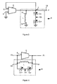
- this oscillator 1 comprises an amplifier 5 and an oscillating network 6 of the LC type. having an inductance L.
- a first terminal 10 of the inductor L is connected to the ground and a second terminal 11 of the inductor is connected to the output of the amplifier 5.
- the second terminal 11 of the inductor L is also connected to a feedback terminal 7 connected to a first input 8 of the amplifier 5.
- a second input 9 of the amplifier is connected to ground.
- the feedback terminal 7 is connected to the ground via a first set consisting of a first variable capacitor Cv1 and a first fixed capacity capacitor C1 connected in series, on the one hand, and a second set constituted by by a second variable capacitor Cv2 and a second fixed capacity capacitor C2 connected in series, on the other hand. These two sets are thus arranged in parallel between the feedback terminal 7 and the ground.
- the control voltage Uc may be applied to a terminal disposed between the first variable capacitor Cv1 and the first fixed capacity capacitor C1, and / or to a terminal disposed between the second variable capacitor Cv2 and the second capacitive capacitor C2.
- US6292065 discloses a voltage controlled oscillator having an LC type oscillating module.
- the oscillating module comprises two inductors, a current source and two feedback transistors, which constitute a differential amplifier.
- the oscillating module has two input terminals.
- a set of first variable capacitors is connected between the two input terminals in parallel with a set of second variable capacitors.
- When a common mode voltage is applied to the input terminals the capacity of a pair of first variable capacitors increases and the capacity of a pair of second variable capacitors decreases. This cancels the effect of the common mode voltage on an output frequency of the oscillating module.
- a difference in voltage applied to the input terminals makes it possible to modify the output frequency of the oscillating module.
- US6657509 discloses an LC-type oscillator. Two variable capacitors are each controlled by a potential difference applied between control terminals. The variable capacitors are, furthermore, respectively connected to two output terminals. Each variable capacitor consists of two MOS type transistors constituting themselves variable capacitors. As in US6292065, a set of two transistors is thus connected between the output terminals, in parallel with an assembly constituted by the two other transistors. The capacitance of the transistors increases with the control voltage.
- the object of the invention is to overcome these drawbacks and, more particularly, to produce a voltage controlled oscillator having a linear / monotonic capacitance / voltage characteristic, which makes it possible to obtain a continuous and monotonous gain and whose phase noise is reduced.
- this object is achieved by the appended claims and, more particularly, by the fact that the first and second variable capacitors are connected in series, the capacitance of one of the variable capacitors varying in the same direction as its voltage. control and the capacity of the other variable capacitor varying in opposite direction with respect to its control voltage.
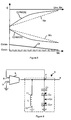
- the voltage-controlled oscillator 1 shown in FIG. 3 is a single output oscillator 13 which comprises an amplifier 5 and an oscillating network 6, of LC type, connected according to FIG. 2.
- the first terminal 10 of the inductor L is connected to the ground and the second terminal 11 of the inductor L is connected to the output of the amplifier 5.
- the second terminal 11 of the inductor L is also connected to the feedback terminal 7 connected to the first input 8 of the amplifier 5.
- the second input 9 of the amplifier is connected to ground.
- the oscillating network 6 comprises a first variable capacitor Cv + and a second variable capacitor Cv- connected in series between the feedback terminal 7 and the ground.
- the inductance L is thus connected in parallel with the first (Cv +) and second (Cv-) variable capacitors.
- a positive terminal of the first variable capacitor Cv + is connected to the ground and a positive terminal of the second variable capacitor Cv- is connected to the feedback terminal 7.
- the first and second variable capacitors Cv + and Cv- are arranged in opposition.
- a negative terminal of the first variable capacitor Cv + is connected to a negative terminal of the second variable capacitor Cv-.
- the first Cv + and second Cv-variable capacitors thus have a common terminal, connected to their respective negative terminals.
- the control voltage Uc of the oscillator 1 is applied to the terminal common to the variable capacitors Cv + and Cv-.
- the capacitance of the first variable capacitor Cv + varies in the same direction as its control voltage, while the capacitance of the second variable capacitor Cv- varies inversely with respect to its control voltage, that is to say that the capacitance decreases when the control voltage of the second variable capacitor Cv- increases.
- the control voltage is set in the conventional control voltage direction of the variable capacitor type used.
- the variable capacitor is, for example, constituted by a MOSFET type transistor whose source and drain are connected.
- the negative terminal of the variable capacitor is thus constituted by the connected drain and source, and the positive terminal of the variable capacitor is constituted by the gate of the transistor.
- variable capacitors Cv + and Cv- can be constituted by any appropriate means and, more particularly, by varactors, of diode or transistor type, or by MEMs-based capacitors.
- the variable capacitor Cv + whose capacitance varies in the same direction as its control voltage may notably consist of a PMOS transistor.
- the variable capacitor Cv- whose capacitance varies inversely with respect to its control voltage is, for example, constituted by an NMOS transistor.
- N + / N / N + type NMOS transistors and P + / P / P + PMOS transistors are preferably used.
- the voltage-controlled oscillator 1 shown in FIG. 4 is a differential output oscillator and comprises, as previously, a first variable capacitor Cv + and a second variable capacitor Cv-connected. in series and in opposition.
- the set of first and second variable capacitors Cv + and Cv- is connected, in parallel with the inductance L, between the input 8 and the output of the amplifier 5.
- the amplifier 5 receives, at its input 8, a signal having a frequency F2.
- FIG. 5 illustrates an example of the non-linear variations in the capacitance of each of the variable capacitors Cv + and Cv- respectively constituted by PMOS and NMOS transistors, respectively as a function of their corresponding control voltages Uv + and Uv- (abscissa at the top of Figure 5).
- the capacitance C (PMOS) of the capacitor PMOS increases when the voltage Uv + applied to its terminals increases, in the conventional sense, while the capacitance C (NMOS) of the capacitor NMOS decreases as the voltage Uv- applied to its terminals increases.
- FIG. 5 also illustrates, as a function of the control voltage Uc of the oscillator (abscissa at the bottom of FIG. 5), the variations of the total capacitance Ct, that is to say the capacitance / voltage characteristic, of the oscillating network 6 shown in Figure 3.
- the series of first (Cv +) and second (Cv-) variable capacitors makes it possible to obtain substantially linear variations in the total capacitance Ct of the oscillating network 6, as a function of the voltage of Uc control.
- the slope of the curve representing the total capacitance Ct is smaller, in absolute value, than the average slopes Mp and Mn of the curves respectively representing the capacitances C (PMOS) and C (NMOS) capacitors PMOS and NMOS.
- the difference between the minimum values Ctmin and maximum Ctmax of the total capacitance Ct is smaller than the deviation of the extreme values of each of the capacitors C (PMOS) and C (NMOS), which makes it possible to obtain a gain K lower and, thus, the phase noise is reduced.
- the series of variable capacitors Cv + and Cv- then has a common linear and monotonic capacitance / voltage characteristic without discontinuity.
- this series does not require changing the polarizations of the capacitors or switching from one capacitor to another.
- the capacitance / common voltage characteristic has a constant slope over a range of the control voltage Uc, for example between 0V and 1.2V, which is greater than the range of the control voltage of the prior art.
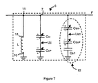
- FIG. 6 represents a circuit according to FIG. 3 further comprising a capacitor C1 having a fixed capacitance and connected in series with the first and second variable capacitors Cv + and Cv-, in particular between the feedback terminal 7, on the one hand , and the set formed by the variable capacitors Cv + and Cv-, on the other hand.
- the capacitor C1 with fixed capacitance can also be placed in parallel with the variable capacitors according to whether it is desired to reduce or increase the overall capacitance.
- FIG. 7 represents a circuit according to FIG. 3 further comprising an additional series 12 connected between the ground and the feedback terminal 7, in parallel with the series formed by the first (Cv +) and second (Cv-) variable capacitors.
- the additional series 12 comprises at least a first additional variable capacitor Csv + and a second additional variable capacitor Csv-connected in opposition.
- An additional control voltage Usc is applied to the common terminal at the negative terminals of the first and second additional variable capacitors Csv + and Csv-.
- the additional series 12 comprises, optionally, an additional capacitor Cs1 with fixed capacity.
- the capacitance of the first additional variable capacitor Csv + varies in the same direction as its control voltage and the capacitance of the second additional variable capacitor Csv- varies inversely with respect to its control voltage.
- the additional capacitor Cs1 with fixed capacitance can also be connected in parallel with the set of additional variable capacitors.
- the positive terminals of the first and second variable capacitors may be connected to a common terminal (not shown), the control voltage of the oscillating network being, as previously, applied to the common terminal to the first and second variable capacitors.
- one or more capacitors with fixed capacity can be connected between the first variable capacitor Cv +, on the one hand, and the second variable capacitor Cv-, on the other hand, or between the mass, on the one hand, and the set of variable capacitors Cv + and Cv-, on the other hand.
- an alternation of first (Cv +) and second (Cv-) capacitors may be connected in series, for example between ground and terminal 7, possibly in combination with capacitors with fixed capacitance.
- each additional series 12 is connected between the terminal 7 and the ground, each series comprising at least first (Csv +) and second (Csv-) additional variable capacitors and, optionally, fixed or additional variables.
Landscapes
- Engineering & Computer Science (AREA)
- Power Engineering (AREA)
- Inductance-Capacitance Distribution Constants And Capacitance-Resistance Oscillators (AREA)
- Oscillators With Electromechanical Resonators (AREA)
- Filters And Equalizers (AREA)
Abstract
Description
- L'invention concerne un oscillateur contrôlé en tension comportant un amplificateur et un réseau oscillant comportant une inductance et au moins des premier et second condensateurs variables ayant chacun une capacité variant en fonction de sa tension de commande.
- Un oscillateur contrôlé en tension (« Voltage Controlled Oscillator : VCO ») fournit des signaux oscillants dont la fréquence varie en fonction d'une tension de contrôle Uc. Le gain de l'oscillateur contrôlé en tension est défini par le rapport K = F/Uc entre la fréquence F de ses signaux de sortie et la tension de contrôle Uc appliquée sur son entrée. Le gain varie généralement en fonction de la tension de contrôle Uc appliquée.
- Les oscillateurs contrôlés en tension sont souvent utilisés dans des boucles à verrouillage de phase, comme représenté à la figure 1. Une telle boucle comporte classiquement un oscillateur 1 contrôlé en tension, dont l'entrée est connectée, par l'intermédiaire d'un filtre 2, à la sortie d'un comparateur de phase 3 et dont la sortie, qui constitue la sortie de la boucle, est connectée à une première entrée du comparateur de phase 3, éventuellement par l'intermédiaire d'un diviseur de fréquence 4. Des signaux d'horloge, ayant une fréquence de référence Fref prédéterminée et par exemple fournis par un oscillateur à quartz, sont appliqués sur une seconde entrée du comparateur de phase 3.
- La tension de contrôle Uc de l'oscillateur est ainsi fonction de la différence entre la fréquence Fs des signaux de sortie de l'oscillateur 1, éventuellement affectée d'un coefficient de division, et de la fréquence de référence Fref. Quand la boucle est verrouillée, la fréquence Fs de sortie est ainsi égale à la fréquence de référence Fref ou à un multiple de celle-ci.
- Une telle boucle à verrouillage de phase est utilisée dans de nombreux circuits nécessitant une synthèse de fréquence, en particulier dans le domaine des radio-fréquences, pour la réception de signaux modulés. Plusieurs standards de transmission, par exemple des standards de type GSM, GPS ou DCS, des standards utilisant la technologie Bluetooth ou un réseau local sans fil (WLAN), sont souvent utilisés dans un même récepteur, notamment dans les téléphones portables. Il est alors souhaitable de pouvoir passer rapidement d'un standard à une autre, par exemple d'un standard de type GSM à un standard de type Bluetooth.
- Le passage d'un standard à l'autre, c'est-à-dire d'une bande de fréquence à une autre, peut provoquer le décrochage de la boucle à verrouillage de phase, c'est-à-dire que l'oscillateur contrôlé en tension ne fournit plus aucun signal. Afin d'éviter le décrochage de la boucle, on cherche à construire des oscillateurs 1 dont les variations de la fréquence F avec la tension de contrôle Uc sont linéaires et monotones, c'est-à-dire dont le gain K = F/Uc est une constante.
- Un oscillateur contrôlé en tension comporte typiquement un amplificateur et un réseau oscillant de type LC. Le réseau oscillant est très important, car de sa conception dépendent les performances du circuit, par exemple le bruit de phase, le coefficient de qualité, la fréquence d'oscillation, etc... De manière générale, la fréquence F de sortie de l'oscillateur contrôlé en tension est fonction de la valeur d'une l'inductance L du réseau oscillant et de la capacité totale Ct du réseau oscillant :

- Dans la plupart des cas, la capacité totale Ct et la fréquence d'oscillation F varient de manière non-linéaire avec la tension de contrôle.
- Actuellement, deux techniques principales sont utilisées pour la conception d'oscillateurs contrôlés en tension ayant une caractéristique capacité/tension linéaire.
- Une première technique consiste à utiliser un condensateur variable dans une gamme restreinte de la tension de contrôle Uc, dans laquelle la capacité varie linéairement. Cependant, ceci nécessite de réduire la plage de variation de la tension de contrôle. Cette technique permet d'obtenir une caractéristique capacité/tension linéaire mais le gain de l'oscillateur est, dans ce cas, très grand et le bruit de phase est ainsi important. De plus, la plage de tension étant réduite, l'asservissement d'une boucle à verrouillage de phase est plus difficile à réaliser et une stabilité de la boucle est difficile à atteindre.
- Une deuxième technique consiste à polariser différemment des condensateurs variables connectés en parallèle. Cette technique permet d'obtenir une caractéristique capacité/tension linéaire. Cependant, cette technique est difficile à réaliser.
- Le brevet US6396356 décrit un oscillateur 1 contrôlé en tension comportant plusieurs condensateurs variables dont les parties linéaires des caractéristiques capacité/tension sont utilisées successivement. Comme illustré à la figure 2, cet oscillateur 1 comporte un amplificateur 5 et un réseau oscillant 6 de type LC comportant une inductance L. Une première borne 10 de l'inductance L est connectée à la masse et une seconde borne 11 de l'inductance est connectée à la sortie de l'amplificateur 5. La seconde borne 11 de l'inductance L est également connectée à une borne 7 de rétroaction reliée à une première entrée 8 de l'amplificateur 5. Une seconde entrée 9 de l'amplificateur est connectée à la masse. La borne 7 de rétroaction est reliée à la masse par l'intermédiaire d'un premier ensemble constitué par un premier condensateur variable Cv1 et un premier condensateur à capacité fixe C1 connectés en série, d'une part, et d'un second ensemble constitué par un second condensateur variable Cv2 et un second condensateur à capacité fixe C2 connectés en série, d'autre part. Ces deux ensembles sont ainsi disposés en parallèle entre la borne 7 de rétroaction et la masse. La tension de contrôle Uc peut être appliquée à une borne disposée entre le premier condensateur variable Cv1 et le premier condensateur à capacité fixe C1, et/ou à une borne disposée entre le second condensateur variable Cv2 et le second condensateur à capacité fixe C2. Lors d'une commutation d'un condensateur variable à l'autre, la tension de contrôle Uc varie de manière discontinue, ce qui peut provoquer le décrochage d'une boucle à verrouillage de phase comportant cet oscillateur. Par ailleurs, cet oscillateur présente un écart important entre les valeurs minimale et maximale de la capacité totale et, ainsi, un bruit de phase important.
- Le document US6292065 décrit un oscillateur contrôlé en tension comportant un module oscillant de type LC. Le module oscillant comprend deux inductances, une source de courant et deux transistors de rétroaction, qui constituent un amplificateur différentiel. Le module oscillant comporte deux bornes d'entrée. Un ensemble de premiers condensateurs variables est connecté, entre les deux bornes d'entrée, en parallèle avec un ensemble de seconds condensateurs variables. Lorsqu'une tension de mode commun est appliquée aux bornes d'entrée, la capacité d'une paire de premiers condensateurs variables augmente et la capacité d'une paire de seconds condensateurs variables diminue. Ceci annule l'effet de la tension de mode commun sur une fréquence de sortie du module oscillant. Par contre, une différence de tension appliquée aux bornes d'entrée permet de modifier la fréquence de sortie du module oscillant.
- Le document US6657509 décrit un oscillateur de type LC. Deux condensateurs variables sont contrôlés chacun par une différence de potentiel appliquée entre des bornes de contrôle. Les condensateurs variables sont, de plus, connectés respectivement à deux bornes de sortie. Chaque condensateur variable est constitué par deux transistors de type MOS constituant eux-mêmes des condensateurs variables. Comme dans le document US6292065, un ensemble de deux transistors est ainsi connecté entre les bornes de sortie, en parallèle avec un ensemble constitué par les deux autres transistors. La capacité des transistors augmente avec la tension de contrôle.
- L'invention a pour but de surmonter ces inconvénients et, plus particulièrement, de réaliser un oscillateur contrôlé en tension ayant une caractéristique capacité/tension linéaire et monotone, permettant d'obtenir un gain continue et monotone et dont le bruit de phase est réduit.
- Selon l'invention, ce but est atteint par les revendications annexées et, plus particulièrement, par le fait que les premier et second condensateurs variables sont connectés en série, la capacité de l'un des condensateurs variables variant dans le même sens que sa tension de commande et la capacité de l'autre condensateur variable variant en sens inverse par rapport à sa tension de commande.
- D'autres avantages et caractéristiques ressortiront plus clairement de la description qui va suivre de modes particuliers de réalisation de l'invention donnés à titre d'exemples non limitatifs et représentés aux dessins annexés, dans lesquels :
- La figure 1 illustre schématiquement une boucle à verrouillage de phase de type classique.
- La figure 2 illustre un oscillateur contrôlé en tension selon l'art antérieur.
- Les figures 3 et 4 représentent deux modes particuliers de réalisation d'un oscillateur selon l'invention.
- La figure 5 illustre les variations de la capacité totale d'un oscillateur selon la figure 3 en fonction de sa tension de contrôle Uc ainsi que les variations de la capacité de chacun des condensateurs variables en fonction de sa tension de commande.
- Les figures 6 et 7 représentent deux modes particuliers de réalisation d'un oscillateur selon l'invention.
- L'oscillateur 1 contrôlé en tension représenté à la figure 3 est un oscillateur à sortie unique 13 qui comporte un amplificateur 5 et un réseau oscillant 6, de type LC, connectés selon la figure 2.
- Ainsi, la première borne 10 de l'inductance L est connectée à la masse et la seconde borne 11 de l'inductance L est connectée à la sortie de l'amplificateur 5. La seconde borne 11 de l'inductance L est également connectée à la borne 7 de rétroaction reliée à la première entrée 8 de l'amplificateur 5. La seconde entrée 9 de l'amplificateur est connectée à la masse.
- Le réseau oscillant 6 comporte un premier condensateur variable Cv+ et un second condensateur variable Cv- connectés en série entre la borne 7 de rétroaction et la masse. Dans le mode de réalisation particulier représenté, l'inductance L est ainsi connectée en parallèle avec les premier (Cv+) et second (Cv-) condensateurs variables. Une borne positive du premier condensateur variable Cv+ est connectée à la masse et une borne positive du second condensateur variable Cv- est connectée à la borne 7 de rétroaction. Sur la figure 3, les premier et second condensateurs variables Cv+ et Cv- sont disposés en opposition.
- Sur la figure 3, une borne négative du premier condensateur variable Cv+ est connectée à une borne négative du second condensateur variable Cv-. Les premier Cv+ et second Cv- condensateurs variables comportent ainsi une borne commune, reliée à leurs bornes négatives respectives. La tension de contrôle Uc de l'oscillateur 1 est appliquée à la borne commune aux condensateurs variables Cv+ et Cv-.
- La capacité du premier condensateur variable Cv+ varie dans le même sens que sa tension de commande, tandis que la capacité du second condensateur variable Cv- varie en sens inverse par rapport à sa tension de commande, c'est-à-dire que la capacité diminue lorsque la tension de commande du second condensateur variable Cv- augmente. La tension de commande est définie dans le sens conventionnel de tension de commande du type de condensateur variable utilisé.
- En effet, la tension de commande Uv d'un condensateur variable est conventionnellement définie comme la différence de potentiel entre une borne négative et une borne positive du condensateur variable Cv, c'est-à-dire conformément à l'équation Uv=(Uneg-Upos).
- Le condensateur variable est, par exemple, constitué par un transistor de type MOSFET dont la source et le drain sont reliés. La borne négative du condensateur variable est ainsi constituée par les drain et source reliés et la borne positive du condensateur variable est constituée par la grille du transistor. La tension de commande d'un MOSFET est définie par la tension Udg appliquée entre le drain et la grille, c'est-à-dire conformément à l'équation Udg=Vd-Vg.
- Les condensateurs variables Cv+ et Cv- peuvent être constitués par tout moyen approprié et, plus particulièrement, par des varactors, de type diode ou de type transistor, ou par des capacités à base de MEMs. Le condensateur variable Cv+ dont la capacité varie dans le même sens que sa tension de commande peut notamment être constitué par un transistor PMOS. Le condensateur variable Cv- dont la capacité varie en sens inverse par rapport à sa tension de commande est, par exemple, constitué par un transistor NMOS. On utilise, de préférence, des transistors NMOS de type N+/N/N+ et des transistors PMOS de type P+/P/P+.
- L'oscillateur 1 contrôlé en tension représenté à la figure 4 est un oscillateur à sortie différentielle et comporte, comme précédemment, un premier condensateur variable Cv+ et un second condensateur variable Cv- connectés en série et en opposition. L'ensemble des premier et second condensateurs variables Cv+ et Cv- est connecté, en parallèle avec l'inductance L, entre l'entrée 8 et la sortie de l'amplificateur 5. L'amplificateur 5 reçoit, à son entrée 8, un signal ayant une fréquence F2.
- La figure 5 illustre un exemple des variations non-linéaires de la capacité de chacun des condensateurs variables Cv+ et Cv-, constitués respectivement par des transistors PMOS et NMOS, respectivement en fonction de leurs tensions de commande correspondantes Uv+ et Uv- (abscisse en haut de la figure 5).
- La capacité C(PMOS) du condensateur PMOS augmente lorsque la tension Uv+ appliquée à ses bornes augmente, dans le sens conventionnel, Tandis que la capacité C(NMOS) du condensateur NMOS diminue lorsque la tension Uv- appliquée à ses bornes augmente.
- La figure 5 illustre également, en fonction de la tension de contrôle Uc de l'oscillateur (abscisse en bas de la figure 5), les variations de la capacité totale Ct, c'est-à-dire la caractéristique capacité/tension, du réseau oscillant 6 représenté à la figure 3. La mise en série des premier (Cv+) et second (Cv-) condensateurs variables permet d'obtenir des variations sensiblement linéaires de la capacité totale Ct du réseau oscillant 6, en fonction de la tension de contrôle Uc. De plus, la pente de la courbe représentant la capacité totale Ct est inférieure, en valeur absolue, aux pentes moyennes Mp et Mn des courbes représentant respectivement les capacités C(PMOS) et C(NMOS) des condensateurs PMOS et NMOS. Ainsi, l'écart entre les valeurs minimale Ctmin et maximale Ctmax de la capacité totale Ct est plus faible que l'écart des valeurs extrêmes de chacune des capacités C(PMOS) et C(NMOS), ce qui permet d'obtenir un gain K plus faible et, ainsi, le bruit de phase est réduit.
- La série des condensateurs variables Cv+ et Cv- présente alors une caractéristique capacité/tension commune linéaire et monotone sans discontinuité. De plus, cette série ne nécessite pas de changer les polarisations des condensateurs ou de commuter d'un condensateur à l'autre. La caractéristique capacité/tension commune a une pente constante sur une plage de la tension de contrôle Uc, par exemple comprise entre 0V et 1,2V, qui est supérieure à la plage de la tension de contrôle de l'art antérieur.
- La figure 6 représente un circuit selon la figure 3 comportant, de plus, un condensateur C1 ayant une capacité fixe et connecté en série avec les premier et second condensateurs variables Cv+ et Cv-, notamment entre la borne 7 de rétroaction, d'une part, et l'ensemble formé par les condensateurs variables Cv+ et Cv-, d'autre part. Le condensateur C1 à capacité fixe peut aussi être placé en parallèle avec les condensateurs variables selon que l'on veut diminuer ou augmenter la capacité globale.
- La figure 7 représente un circuit selon la figure 3 comportant, de plus, une série supplémentaire 12 connectée entre la masse et la borne 7 de rétroaction, en parallèle avec la série constituée par les premier (Cv+) et second (Cv-) condensateurs variables. La série supplémentaire 12 comporte au moins un premier condensateur variable supplémentaire Csv+ et un second condensateur variable supplémentaire Csv- connectés en opposition. Une tension de contrôle supplémentaire Usc est appliquée à la borne commune aux bornes négatives des premier et second condensateurs variables supplémentaires Csv+ et Csv-. La série supplémentaire 12 comporte, éventuellement, un condensateur supplémentaire Cs1 à capacité fixe. La capacité du premier condensateur variable supplémentaire Csv+ varie dans le même sens que sa tension de commande et la capacité du second condensateur variable supplémentaire Csv- varie en sens inverse par rapport à sa tension de commande. Comme précédemment, le condensateur supplémentaire Cs1 à capacité fixe peut aussi être connecté en parallèle avec l'ensemble des condensateurs variables supplémentaires.
- L'invention n'est pas limitée aux modes de réalisation particuliers représentés. En particulier, les bornes positives des premier et second condensateurs variables peuvent être reliées à une borne commune (non-représenté), la tension de contrôle du réseau oscillant étant, comme précédemment, appliquée à la borne commune aux premier et second condensateurs variables.
- Par ailleurs, un ou plusieurs condensateurs à capacité fixe (C1, C2, Cs1, etc...) peuvent être connectés entre le premier condensateur variable Cv+, d'une part, et le second condensateur variable Cv-, d'autre part, ou alors entre la masse, d'une part, et l'ensemble des condensateurs variables Cv+ et Cv-, d'autre part. Par ailleurs, une alternance de premiers (Cv+) et seconds (Cv-) condensateurs peut être connectée en série, par exemple entre la masse et la borne 7, éventuellement en combinaison avec des condensateurs à capacité fixe.
- Dans un mode de réalisation non-représenté, plusieurs séries supplémentaires 12 sont connectées entre la borne 7 et la masse, chaque série comportant au moins des premier (Csv+) et second (Csv-) condensateurs variables supplémentaires et, éventuellement, des capacités fixes ou variables supplémentaires.
Claims (6)
- Oscillateur (1) contrôlé en tension comportant un amplificateur (5) et un réseau oscillant (6) comportant une inductance (L) et au moins des premier et second condensateurs variables (Cv) ayant chacun une capacité variant en fonction de sa tension de commande, oscillateur caractérisé en ce que les premier et second condensateurs variables sont connectés en série, la capacité de l'un des condensateurs variables (Cv+) variant dans le même sens que sa tension de commande et la capacité de l'autre condensateur variable (Cv-) variant en sens inverse par rapport à sa tension de commande.
- Oscillateur selon la revendication 1, caractérisé en ce que les premier et second condensateurs variables (Cv+, Cv-) sont constitués par des transistors, respectivement de type PMOS et NMOS.
- Oscillateur selon l'une des revendications 1 et 2, caractérisé en ce qu'au moins un condensateur (C1) ayant une capacité fixe est connecté en série ou en parallèle avec les premier et second condensateurs variables (Cv+, Cv-).
- Oscillateur selon l'une quelconque des revendications 1 à 3, caractérisé en ce qu'au moins une série supplémentaire (12) de premier et second condensateurs variables supplémentaires (Csv+, Csv-) est connectée en parallèle avec les premier et second condensateurs variables (Cv+, Cv-).
- Oscillateur selon la revendication 4, caractérisé en ce qu'au moins un condensateur supplémentaire (Cs1) ayant une capacité fixe est connecté en série ou en parallèle avec les premier et second condensateurs variables supplémentaires (Csv+, Csv-).
- Oscillateur selon l'une quelconque des revendications 1 à 5, caractérisé en ce que les premier (Cv+) et second (Cv-) condensateurs variables sont connectés en opposition.
Applications Claiming Priority (1)
| Application Number | Priority Date | Filing Date | Title |
|---|---|---|---|
| FR0408121A FR2873516B1 (fr) | 2004-07-22 | 2004-07-22 | Oscillateur controle en tension a capacite lineaire |
Publications (2)
| Publication Number | Publication Date |
|---|---|
| EP1619788A1 true EP1619788A1 (fr) | 2006-01-25 |
| EP1619788B1 EP1619788B1 (fr) | 2007-07-25 |
Family
ID=34942683
Family Applications (1)
| Application Number | Title | Priority Date | Filing Date |
|---|---|---|---|
| EP05354024A Expired - Lifetime EP1619788B1 (fr) | 2004-07-22 | 2005-06-09 | Oscillateur contrôlé en tension à capacité linéaire |
Country Status (6)
| Country | Link |
|---|---|
| US (1) | US7250824B2 (fr) |
| EP (1) | EP1619788B1 (fr) |
| JP (1) | JP4898160B2 (fr) |
| AT (1) | ATE368324T1 (fr) |
| DE (1) | DE602005001729T2 (fr) |
| FR (1) | FR2873516B1 (fr) |
Cited By (1)
| Publication number | Priority date | Publication date | Assignee | Title |
|---|---|---|---|---|
| CN103532547A (zh) * | 2012-07-03 | 2014-01-22 | 西门子公司 | 频率调制器和具有频率调制器的磁共振断层造影仪 |
Families Citing this family (3)
| Publication number | Priority date | Publication date | Assignee | Title |
|---|---|---|---|---|
| JP4837501B2 (ja) * | 2006-09-06 | 2011-12-14 | 浜松ホトニクス株式会社 | Ad変換回路および光検出装置 |
| US20100073096A1 (en) * | 2008-09-22 | 2010-03-25 | Texas Instruments Incorporated | Micro electro-mechanical system based programmable frequency synthesizer and method of operation thereof |
| US9716188B2 (en) * | 2013-08-30 | 2017-07-25 | Qualcomm Incorporated | Metal oxide semiconductor (MOS) capacitor with improved linearity |
Citations (3)
| Publication number | Priority date | Publication date | Assignee | Title |
|---|---|---|---|---|
| US6292065B1 (en) | 2000-01-27 | 2001-09-18 | International Business Machines Corporation | Differential control topology for LC VCO |
| US6396356B1 (en) | 1999-05-24 | 2002-05-28 | Level One Communications, Inc. | Linearization scheme for voltage controlled oscillator |
| US6657509B1 (en) | 2001-01-25 | 2003-12-02 | National Semiconductor Corporation | Differentially controlled varactor |
Family Cites Families (9)
| Publication number | Priority date | Publication date | Assignee | Title |
|---|---|---|---|---|
| US5493715A (en) * | 1994-08-01 | 1996-02-20 | Motorola, Inc. | Multi-range voltage controlled resonant circuit |
| JPH08256016A (ja) * | 1995-03-16 | 1996-10-01 | Hitachi Denshi Ltd | Fm復調器 |
| DE19652146B4 (de) * | 1996-12-14 | 2006-06-29 | Sennheiser Electronic Gmbh & Co. Kg | Rauscharme Oszillatorschaltung |
| US6075421A (en) * | 1998-01-30 | 2000-06-13 | Motorola, Inc. | Voltage controlled oscillator |
| JP2001308638A (ja) * | 2000-04-18 | 2001-11-02 | Alps Electric Co Ltd | 電圧制御発振器 |
| JP2003304118A (ja) * | 2002-04-09 | 2003-10-24 | Mitsubishi Electric Corp | Lc発振回路 |
| JP2004147310A (ja) * | 2002-10-03 | 2004-05-20 | Matsushita Electric Ind Co Ltd | 電圧制御発振器、無線通信機器、電圧制御発振方法 |
| JP2004186776A (ja) * | 2002-11-29 | 2004-07-02 | Fujitsu Ltd | Pll回路 |
| US7064622B2 (en) * | 2004-03-29 | 2006-06-20 | Agere Systems Inc. | Dual differential LC voltage-controlled oscillator |
-
2004
- 2004-07-22 FR FR0408121A patent/FR2873516B1/fr not_active Expired - Fee Related
-
2005
- 2005-06-09 AT AT05354024T patent/ATE368324T1/de not_active IP Right Cessation
- 2005-06-09 EP EP05354024A patent/EP1619788B1/fr not_active Expired - Lifetime
- 2005-06-09 DE DE602005001729T patent/DE602005001729T2/de not_active Expired - Lifetime
- 2005-06-15 US US11/152,075 patent/US7250824B2/en not_active Expired - Fee Related
- 2005-07-21 JP JP2005211705A patent/JP4898160B2/ja not_active Expired - Fee Related
Patent Citations (3)
| Publication number | Priority date | Publication date | Assignee | Title |
|---|---|---|---|---|
| US6396356B1 (en) | 1999-05-24 | 2002-05-28 | Level One Communications, Inc. | Linearization scheme for voltage controlled oscillator |
| US6292065B1 (en) | 2000-01-27 | 2001-09-18 | International Business Machines Corporation | Differential control topology for LC VCO |
| US6657509B1 (en) | 2001-01-25 | 2003-12-02 | National Semiconductor Corporation | Differentially controlled varactor |
Cited By (2)
| Publication number | Priority date | Publication date | Assignee | Title |
|---|---|---|---|---|
| CN103532547A (zh) * | 2012-07-03 | 2014-01-22 | 西门子公司 | 频率调制器和具有频率调制器的磁共振断层造影仪 |
| US9780727B2 (en) | 2012-07-03 | 2017-10-03 | Siemens Aktiengesellschaft | Frequency modulator and magnetic resonance tomography system with a frequency modulator |
Also Published As
| Publication number | Publication date |
|---|---|
| DE602005001729T2 (de) | 2008-04-10 |
| FR2873516B1 (fr) | 2007-02-02 |
| ATE368324T1 (de) | 2007-08-15 |
| JP4898160B2 (ja) | 2012-03-14 |
| JP2006042338A (ja) | 2006-02-09 |
| FR2873516A1 (fr) | 2006-01-27 |
| US7250824B2 (en) | 2007-07-31 |
| DE602005001729D1 (de) | 2007-09-06 |
| US20060017513A1 (en) | 2006-01-26 |
| EP1619788B1 (fr) | 2007-07-25 |
Similar Documents
| Publication | Publication Date | Title |
|---|---|---|
| EP1265352B1 (fr) | Circuit oscillateur différentiel comprenant un résonateur électromécanique | |
| EP1909386A1 (fr) | Circuit de capacité négative pour applications hautes fréquences | |
| FR2926689A1 (fr) | Dispositif electrique a resonateur a large plage de variation en frequences | |
| FR2920924A1 (fr) | Oscillateur a large bande controle en tension. | |
| EP2810368B1 (fr) | Oscillateur commandé en tension utilisant un condensateur variable et boucle à verrouillage de phase utilisant celui-ci | |
| FR2602380A1 (fr) | Circuit gyrateur simulant une inductance | |
| US7573347B2 (en) | Digitally controlled oscillator device and method for generating an oscillating signal with a digitally controlled phase locked loop | |
| US7623837B2 (en) | Receiver for an integrated heterodyne communication system including BAW-type resonators | |
| FR2947118A1 (fr) | Dispositif d'oscillateur multibandes frequentielles | |
| El Oualkadi et al. | Fully integrated high-Q switched capacitor bandpass filter with center frequency and bandwidth tuning | |
| JP2011009849A (ja) | Pll周波数シンセサイザ | |
| FR2864728A1 (fr) | Circuit electronique integre comportant un resonateur accordable | |
| FR2864727A1 (fr) | Circuit electronique comportant un resonateur destine a etre integre dans un produit semi-conducteur | |
| EP1619788B1 (fr) | Oscillateur contrôlé en tension à capacité linéaire | |
| EP0661816B1 (fr) | Synthétiseur de fréquences à boucle unique et ensemble électronique comportant un tel synthétiseur | |
| FR2688955A1 (fr) | Filtre accordable haute frequence. | |
| EP1885063A1 (fr) | Circuit de filtrage doté de résonateurs accoustiques | |
| FR2644647A1 (fr) | Oscillateur hyperfrequence commande en tension | |
| EP1608073B1 (fr) | Oscillateur contrôlé en tension | |
| FR2864726A1 (fr) | Boucle a verrouillage d'amplitude integrable dotee d'un resonateur acoustique | |
| FR2864733A1 (fr) | Boucle a verrouillage de phase integrable dotee d'un resonateur acoustique | |
| FR2853162A1 (fr) | Oscillateur commande en tension | |
| EP1187308B1 (fr) | Oscillateur commande en tension | |
| FR2905042A1 (fr) | Circuit electronique integre comportant un resonnateur accordable | |
| EP1052772B1 (fr) | Dispositif et procédé pour produire un signal filtré |
Legal Events
| Date | Code | Title | Description |
|---|---|---|---|
| PUAI | Public reference made under article 153(3) epc to a published international application that has entered the european phase |
Free format text: ORIGINAL CODE: 0009012 |
|
| AK | Designated contracting states |
Kind code of ref document: A1 Designated state(s): AT BE BG CH CY CZ DE DK EE ES FI FR GB GR HU IE IS IT LI LT LU MC NL PL PT RO SE SI SK TR |
|
| AX | Request for extension of the european patent |
Extension state: AL BA HR LV MK YU |
|
| 17P | Request for examination filed |
Effective date: 20060502 |
|
| AKX | Designation fees paid |
Designated state(s): AT BE BG CH CY CZ DE DK EE ES FI FR GB GR HU IE IS IT LI LT LU MC NL PL PT RO SE SI SK TR |
|
| GRAP | Despatch of communication of intention to grant a patent |
Free format text: ORIGINAL CODE: EPIDOSNIGR1 |
|
| GRAS | Grant fee paid |
Free format text: ORIGINAL CODE: EPIDOSNIGR3 |
|
| GRAA | (expected) grant |
Free format text: ORIGINAL CODE: 0009210 |
|
| AK | Designated contracting states |
Kind code of ref document: B1 Designated state(s): AT BE BG CH CY CZ DE DK EE ES FI FR GB GR HU IE IS IT LI LT LU MC NL PL PT RO SE SI SK TR |
|
| REG | Reference to a national code |
Ref country code: GB Ref legal event code: FG4D Free format text: NOT ENGLISH |
|
| REG | Reference to a national code |
Ref country code: CH Ref legal event code: EP |
|
| REG | Reference to a national code |
Ref country code: IE Ref legal event code: FG4D Free format text: LANGUAGE OF EP DOCUMENT: FRENCH |
|
| REF | Corresponds to: |
Ref document number: 602005001729 Country of ref document: DE Date of ref document: 20070906 Kind code of ref document: P |
|
| PG25 | Lapsed in a contracting state [announced via postgrant information from national office to epo] |
Ref country code: IS Free format text: LAPSE BECAUSE OF FAILURE TO SUBMIT A TRANSLATION OF THE DESCRIPTION OR TO PAY THE FEE WITHIN THE PRESCRIBED TIME-LIMIT Effective date: 20071125 Ref country code: FI Free format text: LAPSE BECAUSE OF FAILURE TO SUBMIT A TRANSLATION OF THE DESCRIPTION OR TO PAY THE FEE WITHIN THE PRESCRIBED TIME-LIMIT Effective date: 20070725 Ref country code: ES Free format text: LAPSE BECAUSE OF FAILURE TO SUBMIT A TRANSLATION OF THE DESCRIPTION OR TO PAY THE FEE WITHIN THE PRESCRIBED TIME-LIMIT Effective date: 20071105 Ref country code: LT Free format text: LAPSE BECAUSE OF FAILURE TO SUBMIT A TRANSLATION OF THE DESCRIPTION OR TO PAY THE FEE WITHIN THE PRESCRIBED TIME-LIMIT Effective date: 20070725 Ref country code: PT Free format text: LAPSE BECAUSE OF FAILURE TO SUBMIT A TRANSLATION OF THE DESCRIPTION OR TO PAY THE FEE WITHIN THE PRESCRIBED TIME-LIMIT Effective date: 20071226 Ref country code: BG Free format text: LAPSE BECAUSE OF FAILURE TO SUBMIT A TRANSLATION OF THE DESCRIPTION OR TO PAY THE FEE WITHIN THE PRESCRIBED TIME-LIMIT Effective date: 20071025 |
|
| GBV | Gb: ep patent (uk) treated as always having been void in accordance with gb section 77(7)/1977 [no translation filed] |
Effective date: 20070725 |
|
| PG25 | Lapsed in a contracting state [announced via postgrant information from national office to epo] |
Ref country code: AT Free format text: LAPSE BECAUSE OF FAILURE TO SUBMIT A TRANSLATION OF THE DESCRIPTION OR TO PAY THE FEE WITHIN THE PRESCRIBED TIME-LIMIT Effective date: 20070725 Ref country code: PL Free format text: LAPSE BECAUSE OF FAILURE TO SUBMIT A TRANSLATION OF THE DESCRIPTION OR TO PAY THE FEE WITHIN THE PRESCRIBED TIME-LIMIT Effective date: 20070725 |
|
| REG | Reference to a national code |
Ref country code: IE Ref legal event code: FD4D |
|
| PG25 | Lapsed in a contracting state [announced via postgrant information from national office to epo] |
Ref country code: GR Free format text: LAPSE BECAUSE OF FAILURE TO SUBMIT A TRANSLATION OF THE DESCRIPTION OR TO PAY THE FEE WITHIN THE PRESCRIBED TIME-LIMIT Effective date: 20071026 Ref country code: DK Free format text: LAPSE BECAUSE OF FAILURE TO SUBMIT A TRANSLATION OF THE DESCRIPTION OR TO PAY THE FEE WITHIN THE PRESCRIBED TIME-LIMIT Effective date: 20070725 |
|
| PG25 | Lapsed in a contracting state [announced via postgrant information from national office to epo] |
Ref country code: SK Free format text: LAPSE BECAUSE OF FAILURE TO SUBMIT A TRANSLATION OF THE DESCRIPTION OR TO PAY THE FEE WITHIN THE PRESCRIBED TIME-LIMIT Effective date: 20070725 Ref country code: CZ Free format text: LAPSE BECAUSE OF FAILURE TO SUBMIT A TRANSLATION OF THE DESCRIPTION OR TO PAY THE FEE WITHIN THE PRESCRIBED TIME-LIMIT Effective date: 20070725 Ref country code: IE Free format text: LAPSE BECAUSE OF FAILURE TO SUBMIT A TRANSLATION OF THE DESCRIPTION OR TO PAY THE FEE WITHIN THE PRESCRIBED TIME-LIMIT Effective date: 20070725 Ref country code: GB Free format text: LAPSE BECAUSE OF FAILURE TO SUBMIT A TRANSLATION OF THE DESCRIPTION OR TO PAY THE FEE WITHIN THE PRESCRIBED TIME-LIMIT Effective date: 20070725 |
|
| PLBE | No opposition filed within time limit |
Free format text: ORIGINAL CODE: 0009261 |
|
| STAA | Information on the status of an ep patent application or granted ep patent |
Free format text: STATUS: NO OPPOSITION FILED WITHIN TIME LIMIT |
|
| PG25 | Lapsed in a contracting state [announced via postgrant information from national office to epo] |
Ref country code: SE Free format text: LAPSE BECAUSE OF FAILURE TO SUBMIT A TRANSLATION OF THE DESCRIPTION OR TO PAY THE FEE WITHIN THE PRESCRIBED TIME-LIMIT Effective date: 20071025 Ref country code: RO Free format text: LAPSE BECAUSE OF FAILURE TO SUBMIT A TRANSLATION OF THE DESCRIPTION OR TO PAY THE FEE WITHIN THE PRESCRIBED TIME-LIMIT Effective date: 20070725 |
|
| 26N | No opposition filed |
Effective date: 20080428 |
|
| BERE | Be: lapsed |
Owner name: COMMISSARIAT A L'ENERGIE ATOMIQUE Effective date: 20080630 |
|
| PG25 | Lapsed in a contracting state [announced via postgrant information from national office to epo] |
Ref country code: MC Free format text: LAPSE BECAUSE OF NON-PAYMENT OF DUE FEES Effective date: 20080630 |
|
| PG25 | Lapsed in a contracting state [announced via postgrant information from national office to epo] |
Ref country code: BE Free format text: LAPSE BECAUSE OF NON-PAYMENT OF DUE FEES Effective date: 20080630 |
|
| PG25 | Lapsed in a contracting state [announced via postgrant information from national office to epo] |
Ref country code: EE Free format text: LAPSE BECAUSE OF FAILURE TO SUBMIT A TRANSLATION OF THE DESCRIPTION OR TO PAY THE FEE WITHIN THE PRESCRIBED TIME-LIMIT Effective date: 20070725 |
|
| PG25 | Lapsed in a contracting state [announced via postgrant information from national office to epo] |
Ref country code: SI Free format text: LAPSE BECAUSE OF FAILURE TO SUBMIT A TRANSLATION OF THE DESCRIPTION OR TO PAY THE FEE WITHIN THE PRESCRIBED TIME-LIMIT Effective date: 20070725 |
|
| PG25 | Lapsed in a contracting state [announced via postgrant information from national office to epo] |
Ref country code: CY Free format text: LAPSE BECAUSE OF FAILURE TO SUBMIT A TRANSLATION OF THE DESCRIPTION OR TO PAY THE FEE WITHIN THE PRESCRIBED TIME-LIMIT Effective date: 20070725 |
|
| REG | Reference to a national code |
Ref country code: CH Ref legal event code: PL |
|
| PG25 | Lapsed in a contracting state [announced via postgrant information from national office to epo] |
Ref country code: LI Free format text: LAPSE BECAUSE OF NON-PAYMENT OF DUE FEES Effective date: 20090630 Ref country code: CH Free format text: LAPSE BECAUSE OF NON-PAYMENT OF DUE FEES Effective date: 20090630 |
|
| PG25 | Lapsed in a contracting state [announced via postgrant information from national office to epo] |
Ref country code: LU Free format text: LAPSE BECAUSE OF NON-PAYMENT OF DUE FEES Effective date: 20080609 Ref country code: HU Free format text: LAPSE BECAUSE OF FAILURE TO SUBMIT A TRANSLATION OF THE DESCRIPTION OR TO PAY THE FEE WITHIN THE PRESCRIBED TIME-LIMIT Effective date: 20080126 |
|
| PG25 | Lapsed in a contracting state [announced via postgrant information from national office to epo] |
Ref country code: TR Free format text: LAPSE BECAUSE OF FAILURE TO SUBMIT A TRANSLATION OF THE DESCRIPTION OR TO PAY THE FEE WITHIN THE PRESCRIBED TIME-LIMIT Effective date: 20070725 |
|
| REG | Reference to a national code |
Ref country code: FR Ref legal event code: PLFP Year of fee payment: 12 |
|
| PGFP | Annual fee paid to national office [announced via postgrant information from national office to epo] |
Ref country code: NL Payment date: 20170515 Year of fee payment: 13 |
|
| REG | Reference to a national code |
Ref country code: FR Ref legal event code: PLFP Year of fee payment: 13 |
|
| PGFP | Annual fee paid to national office [announced via postgrant information from national office to epo] |
Ref country code: FR Payment date: 20170630 Year of fee payment: 13 Ref country code: DE Payment date: 20170614 Year of fee payment: 13 |
|
| PGFP | Annual fee paid to national office [announced via postgrant information from national office to epo] |
Ref country code: IT Payment date: 20170619 Year of fee payment: 13 |
|
| REG | Reference to a national code |
Ref country code: DE Ref legal event code: R119 Ref document number: 602005001729 Country of ref document: DE |
|
| REG | Reference to a national code |
Ref country code: NL Ref legal event code: MM Effective date: 20180701 |
|
| PG25 | Lapsed in a contracting state [announced via postgrant information from national office to epo] |
Ref country code: NL Free format text: LAPSE BECAUSE OF NON-PAYMENT OF DUE FEES Effective date: 20180701 |
|
| PG25 | Lapsed in a contracting state [announced via postgrant information from national office to epo] |
Ref country code: FR Free format text: LAPSE BECAUSE OF NON-PAYMENT OF DUE FEES Effective date: 20180630 Ref country code: IT Free format text: LAPSE BECAUSE OF NON-PAYMENT OF DUE FEES Effective date: 20180609 Ref country code: DE Free format text: LAPSE BECAUSE OF NON-PAYMENT OF DUE FEES Effective date: 20190101 |