EP1619276B1 - Homoepitaxial growth of SiC on low off-axis SiC wafers - Google Patents
Homoepitaxial growth of SiC on low off-axis SiC wafers Download PDFInfo
- Publication number
- EP1619276B1 EP1619276B1 EP05014753.7A EP05014753A EP1619276B1 EP 1619276 B1 EP1619276 B1 EP 1619276B1 EP 05014753 A EP05014753 A EP 05014753A EP 1619276 B1 EP1619276 B1 EP 1619276B1
- Authority
- EP
- European Patent Office
- Prior art keywords
- sic
- substrate
- layer
- growth
- homoepitaxial
- Prior art date
- Legal status (The legal status is an assumption and is not a legal conclusion. Google has not performed a legal analysis and makes no representation as to the accuracy of the status listed.)
- Expired - Lifetime
Links
Images



Classifications
-
- C—CHEMISTRY; METALLURGY
- C30—CRYSTAL GROWTH
- C30B—SINGLE-CRYSTAL GROWTH; UNIDIRECTIONAL SOLIDIFICATION OF EUTECTIC MATERIAL OR UNIDIRECTIONAL DEMIXING OF EUTECTOID MATERIAL; REFINING BY ZONE-MELTING OF MATERIAL; PRODUCTION OF A HOMOGENEOUS POLYCRYSTALLINE MATERIAL WITH DEFINED STRUCTURE; SINGLE CRYSTALS OR HOMOGENEOUS POLYCRYSTALLINE MATERIAL WITH DEFINED STRUCTURE; AFTER-TREATMENT OF SINGLE CRYSTALS OR A HOMOGENEOUS POLYCRYSTALLINE MATERIAL WITH DEFINED STRUCTURE; APPARATUS THEREFOR
- C30B29/00—Single crystals or homogeneous polycrystalline material with defined structure characterised by the material or by their shape
- C30B29/10—Inorganic compounds or compositions
- C30B29/36—Carbides
-
- C—CHEMISTRY; METALLURGY
- C30—CRYSTAL GROWTH
- C30B—SINGLE-CRYSTAL GROWTH; UNIDIRECTIONAL SOLIDIFICATION OF EUTECTIC MATERIAL OR UNIDIRECTIONAL DEMIXING OF EUTECTOID MATERIAL; REFINING BY ZONE-MELTING OF MATERIAL; PRODUCTION OF A HOMOGENEOUS POLYCRYSTALLINE MATERIAL WITH DEFINED STRUCTURE; SINGLE CRYSTALS OR HOMOGENEOUS POLYCRYSTALLINE MATERIAL WITH DEFINED STRUCTURE; AFTER-TREATMENT OF SINGLE CRYSTALS OR A HOMOGENEOUS POLYCRYSTALLINE MATERIAL WITH DEFINED STRUCTURE; APPARATUS THEREFOR
- C30B25/00—Single-crystal growth by chemical reaction of reactive gases, e.g. chemical vapour-deposition growth
- C30B25/02—Epitaxial-layer growth
-
- C—CHEMISTRY; METALLURGY
- C30—CRYSTAL GROWTH
- C30B—SINGLE-CRYSTAL GROWTH; UNIDIRECTIONAL SOLIDIFICATION OF EUTECTIC MATERIAL OR UNIDIRECTIONAL DEMIXING OF EUTECTOID MATERIAL; REFINING BY ZONE-MELTING OF MATERIAL; PRODUCTION OF A HOMOGENEOUS POLYCRYSTALLINE MATERIAL WITH DEFINED STRUCTURE; SINGLE CRYSTALS OR HOMOGENEOUS POLYCRYSTALLINE MATERIAL WITH DEFINED STRUCTURE; AFTER-TREATMENT OF SINGLE CRYSTALS OR A HOMOGENEOUS POLYCRYSTALLINE MATERIAL WITH DEFINED STRUCTURE; APPARATUS THEREFOR
- C30B25/00—Single-crystal growth by chemical reaction of reactive gases, e.g. chemical vapour-deposition growth
- C30B25/02—Epitaxial-layer growth
- C30B25/18—Epitaxial-layer growth characterised by the substrate
-
- C—CHEMISTRY; METALLURGY
- C30—CRYSTAL GROWTH
- C30B—SINGLE-CRYSTAL GROWTH; UNIDIRECTIONAL SOLIDIFICATION OF EUTECTIC MATERIAL OR UNIDIRECTIONAL DEMIXING OF EUTECTOID MATERIAL; REFINING BY ZONE-MELTING OF MATERIAL; PRODUCTION OF A HOMOGENEOUS POLYCRYSTALLINE MATERIAL WITH DEFINED STRUCTURE; SINGLE CRYSTALS OR HOMOGENEOUS POLYCRYSTALLINE MATERIAL WITH DEFINED STRUCTURE; AFTER-TREATMENT OF SINGLE CRYSTALS OR A HOMOGENEOUS POLYCRYSTALLINE MATERIAL WITH DEFINED STRUCTURE; APPARATUS THEREFOR
- C30B25/00—Single-crystal growth by chemical reaction of reactive gases, e.g. chemical vapour-deposition growth
- C30B25/02—Epitaxial-layer growth
- C30B25/18—Epitaxial-layer growth characterised by the substrate
- C30B25/20—Epitaxial-layer growth characterised by the substrate the substrate being of the same materials as the epitaxial layer
-
- H—ELECTRICITY
- H10—SEMICONDUCTOR DEVICES; ELECTRIC SOLID-STATE DEVICES NOT OTHERWISE PROVIDED FOR
- H10P—GENERIC PROCESSES OR APPARATUS FOR THE MANUFACTURE OR TREATMENT OF DEVICES COVERED BY CLASS H10
- H10P14/00—Formation of materials, e.g. in the shape of layers or pillars
- H10P14/20—Formation of materials, e.g. in the shape of layers or pillars of semiconductor materials
-
- H—ELECTRICITY
- H10—SEMICONDUCTOR DEVICES; ELECTRIC SOLID-STATE DEVICES NOT OTHERWISE PROVIDED FOR
- H10P—GENERIC PROCESSES OR APPARATUS FOR THE MANUFACTURE OR TREATMENT OF DEVICES COVERED BY CLASS H10
- H10P14/00—Formation of materials, e.g. in the shape of layers or pillars
- H10P14/20—Formation of materials, e.g. in the shape of layers or pillars of semiconductor materials
- H10P14/24—Formation of materials, e.g. in the shape of layers or pillars of semiconductor materials using chemical vapour deposition [CVD]
-
- H—ELECTRICITY
- H10—SEMICONDUCTOR DEVICES; ELECTRIC SOLID-STATE DEVICES NOT OTHERWISE PROVIDED FOR
- H10P—GENERIC PROCESSES OR APPARATUS FOR THE MANUFACTURE OR TREATMENT OF DEVICES COVERED BY CLASS H10
- H10P14/00—Formation of materials, e.g. in the shape of layers or pillars
- H10P14/20—Formation of materials, e.g. in the shape of layers or pillars of semiconductor materials
- H10P14/29—Formation of materials, e.g. in the shape of layers or pillars of semiconductor materials characterised by the substrates
- H10P14/2901—Materials
- H10P14/2902—Materials being Group IVA materials
- H10P14/2904—Silicon carbide
-
- H—ELECTRICITY
- H10—SEMICONDUCTOR DEVICES; ELECTRIC SOLID-STATE DEVICES NOT OTHERWISE PROVIDED FOR
- H10P—GENERIC PROCESSES OR APPARATUS FOR THE MANUFACTURE OR TREATMENT OF DEVICES COVERED BY CLASS H10
- H10P14/00—Formation of materials, e.g. in the shape of layers or pillars
- H10P14/20—Formation of materials, e.g. in the shape of layers or pillars of semiconductor materials
- H10P14/29—Formation of materials, e.g. in the shape of layers or pillars of semiconductor materials characterised by the substrates
- H10P14/2924—Structures
- H10P14/2925—Surface structures
-
- H—ELECTRICITY
- H10—SEMICONDUCTOR DEVICES; ELECTRIC SOLID-STATE DEVICES NOT OTHERWISE PROVIDED FOR
- H10P—GENERIC PROCESSES OR APPARATUS FOR THE MANUFACTURE OR TREATMENT OF DEVICES COVERED BY CLASS H10
- H10P14/00—Formation of materials, e.g. in the shape of layers or pillars
- H10P14/20—Formation of materials, e.g. in the shape of layers or pillars of semiconductor materials
- H10P14/29—Formation of materials, e.g. in the shape of layers or pillars of semiconductor materials characterised by the substrates
- H10P14/2926—Crystal orientations
-
- H—ELECTRICITY
- H10—SEMICONDUCTOR DEVICES; ELECTRIC SOLID-STATE DEVICES NOT OTHERWISE PROVIDED FOR
- H10P—GENERIC PROCESSES OR APPARATUS FOR THE MANUFACTURE OR TREATMENT OF DEVICES COVERED BY CLASS H10
- H10P14/00—Formation of materials, e.g. in the shape of layers or pillars
- H10P14/20—Formation of materials, e.g. in the shape of layers or pillars of semiconductor materials
- H10P14/32—Formation of materials, e.g. in the shape of layers or pillars of semiconductor materials characterised by intermediate layers between substrates and deposited layers
- H10P14/3202—Materials thereof
- H10P14/3204—Materials thereof being Group IVA semiconducting materials
- H10P14/3208—Silicon carbide
-
- H—ELECTRICITY
- H10—SEMICONDUCTOR DEVICES; ELECTRIC SOLID-STATE DEVICES NOT OTHERWISE PROVIDED FOR
- H10P—GENERIC PROCESSES OR APPARATUS FOR THE MANUFACTURE OR TREATMENT OF DEVICES COVERED BY CLASS H10
- H10P14/00—Formation of materials, e.g. in the shape of layers or pillars
- H10P14/20—Formation of materials, e.g. in the shape of layers or pillars of semiconductor materials
- H10P14/32—Formation of materials, e.g. in the shape of layers or pillars of semiconductor materials characterised by intermediate layers between substrates and deposited layers
- H10P14/3242—Structure
- H10P14/3244—Layer structure
- H10P14/3248—Layer structure consisting of two layers
-
- H—ELECTRICITY
- H10—SEMICONDUCTOR DEVICES; ELECTRIC SOLID-STATE DEVICES NOT OTHERWISE PROVIDED FOR
- H10P—GENERIC PROCESSES OR APPARATUS FOR THE MANUFACTURE OR TREATMENT OF DEVICES COVERED BY CLASS H10
- H10P14/00—Formation of materials, e.g. in the shape of layers or pillars
- H10P14/20—Formation of materials, e.g. in the shape of layers or pillars of semiconductor materials
- H10P14/34—Deposited materials, e.g. layers
- H10P14/3402—Deposited materials, e.g. layers characterised by the chemical composition
- H10P14/3404—Deposited materials, e.g. layers characterised by the chemical composition being Group IVA materials
- H10P14/3408—Silicon carbide
-
- H—ELECTRICITY
- H10—SEMICONDUCTOR DEVICES; ELECTRIC SOLID-STATE DEVICES NOT OTHERWISE PROVIDED FOR
- H10P—GENERIC PROCESSES OR APPARATUS FOR THE MANUFACTURE OR TREATMENT OF DEVICES COVERED BY CLASS H10
- H10P14/00—Formation of materials, e.g. in the shape of layers or pillars
- H10P14/20—Formation of materials, e.g. in the shape of layers or pillars of semiconductor materials
- H10P14/34—Deposited materials, e.g. layers
- H10P14/3402—Deposited materials, e.g. layers characterised by the chemical composition
- H10P14/3414—Deposited materials, e.g. layers characterised by the chemical composition being group IIIA-VIA materials
- H10P14/3416—Nitrides
-
- H—ELECTRICITY
- H10—SEMICONDUCTOR DEVICES; ELECTRIC SOLID-STATE DEVICES NOT OTHERWISE PROVIDED FOR
- H10P—GENERIC PROCESSES OR APPARATUS FOR THE MANUFACTURE OR TREATMENT OF DEVICES COVERED BY CLASS H10
- H10P14/00—Formation of materials, e.g. in the shape of layers or pillars
- H10P14/20—Formation of materials, e.g. in the shape of layers or pillars of semiconductor materials
- H10P14/34—Deposited materials, e.g. layers
- H10P14/3402—Deposited materials, e.g. layers characterised by the chemical composition
- H10P14/3424—Deposited materials, e.g. layers characterised by the chemical composition being Group IIB-VIA materials
- H10P14/3426—Oxides
-
- H—ELECTRICITY
- H10—SEMICONDUCTOR DEVICES; ELECTRIC SOLID-STATE DEVICES NOT OTHERWISE PROVIDED FOR
- H10P—GENERIC PROCESSES OR APPARATUS FOR THE MANUFACTURE OR TREATMENT OF DEVICES COVERED BY CLASS H10
- H10P14/00—Formation of materials, e.g. in the shape of layers or pillars
- H10P14/20—Formation of materials, e.g. in the shape of layers or pillars of semiconductor materials
- H10P14/34—Deposited materials, e.g. layers
- H10P14/3438—Doping during depositing
- H10P14/3441—Conductivity type
-
- H—ELECTRICITY
- H10—SEMICONDUCTOR DEVICES; ELECTRIC SOLID-STATE DEVICES NOT OTHERWISE PROVIDED FOR
- H10P—GENERIC PROCESSES OR APPARATUS FOR THE MANUFACTURE OR TREATMENT OF DEVICES COVERED BY CLASS H10
- H10P14/00—Formation of materials, e.g. in the shape of layers or pillars
- H10P14/20—Formation of materials, e.g. in the shape of layers or pillars of semiconductor materials
- H10P14/34—Deposited materials, e.g. layers
- H10P14/3438—Doping during depositing
- H10P14/3441—Conductivity type
- H10P14/3446—Transition metal elements; Rare earth elements
-
- H—ELECTRICITY
- H10—SEMICONDUCTOR DEVICES; ELECTRIC SOLID-STATE DEVICES NOT OTHERWISE PROVIDED FOR
- H10P—GENERIC PROCESSES OR APPARATUS FOR THE MANUFACTURE OR TREATMENT OF DEVICES COVERED BY CLASS H10
- H10P14/00—Formation of materials, e.g. in the shape of layers or pillars
- H10P14/20—Formation of materials, e.g. in the shape of layers or pillars of semiconductor materials
- H10P14/36—Formation of materials, e.g. in the shape of layers or pillars of semiconductor materials characterised by treatments done before the formation of the materials
-
- Y—GENERAL TAGGING OF NEW TECHNOLOGICAL DEVELOPMENTS; GENERAL TAGGING OF CROSS-SECTIONAL TECHNOLOGIES SPANNING OVER SEVERAL SECTIONS OF THE IPC; TECHNICAL SUBJECTS COVERED BY FORMER USPC CROSS-REFERENCE ART COLLECTIONS [XRACs] AND DIGESTS
- Y10—TECHNICAL SUBJECTS COVERED BY FORMER USPC
- Y10S—TECHNICAL SUBJECTS COVERED BY FORMER USPC CROSS-REFERENCE ART COLLECTIONS [XRACs] AND DIGESTS
- Y10S438/00—Semiconductor device manufacturing: process
- Y10S438/931—Silicon carbide semiconductor
Definitions
- the present invention relates to epitaxial layers grown on SiC substrates having an off-axis angle less than 1 degree. Particularly, the invention is related to a method for accomplishing wafers and devices on SiC substrates having said off-axis angle.
- US patents 4,912,064 and 5,011,549 teach a CVD method for producing device quality SiC films of hexagonal polytypes on substrates with an off-axis angle larger than 1 degree, and preferably between 3 and 12°, along one of the ⁇ 11 2 0> crystallographic directions.
- US patent 5,248,385 teaches a method to homoepitaxially grow SiC films on SiC substrates having an off-axis angle from less than 0.1° to about 6° where the surface of the substrate is subject to a HCl/H2 gas mixture pre-growth etch to eliminate surface features which can act as nucleation sites for foreign polytype inclusions.
- off-axis 4° 4H-SiC (0001) Si designates a 4H polytype SiC substrate with a Si growth surface inclined about 4° from the (0001) basal plane.
- Nakamura et al. [1] teaches that homoepitaxial growth over areas larger than 1 ⁇ 1 mm 2 on 0.2°-off 4H-SiC (0001) Si substrates can be obtained at a C/Si ratio of 1.6, whereas a C/Si ratio of 2 significantly increases the number of surface defects. It shall be noted that in this publication the area of homoepitaxial growth free of polytype inclusions and surface defects (1 ⁇ 1mm 2 ) is too small for acceptable device manufacturing yields. The density of surface defects (150 cm -2 triangular defect and so-called carrot defects in their best sample) is also too high for acceptable device manufacturing yields.
- Nakamura also teaches that homoepitaxial growth over areas larger than 1 ⁇ 1mm 2 are realised on 0.7°-off 4H-SiC (0001) C substrates provided that the surface damage of the substrate is reduced prior to growth by thermal oxidation for 12 hours.
- the density of surface defects 150 cm -2 triangular defect and so-called carrot defects in their epilayer grown on 0.7°-off 4H-SiC (0001) C substrate) is however too high for acceptable device manufacturing yields.
- the substrate preparation prior to growth is not described, but it is mentioned that the lowest density of defects is obtained on commercial as-received substrates. Improper oxidation or plasma treatments on as-received substrates increase the density of triangular shaped surface defects and 3C-inclusions. This shows that the surface quality is a necessary requirement for wide-area homoepitaxial growth on low off-axis SiC substrates. It shall be noted that a specular epitaxial surface is obtained by the authors on only ⁇ 40% of the substrate area.
- Treu et al [5] describes the material cost advantages of reducing the off-axis angle of 3-inch diameter 4H-SiC wafers angle from 8° to 4° and that by changing the C/Si ratio the step bunching appearing on 4° off-axis epilayers could be reduced. However, this affected negatively the background doping and the thickness and doping homogeneity.
- a modified process was developed to reduce step bunching on 4° off-axis wafers, while almost maintaining the other layer properties, but is not described in their publication.
- Kojima et al [6] reported the development of CVD growth conditions suited for homoepitaxial growth on 8°-off 4H-SiC (0001) C substrates.
- a first finding is that, as compared to epitaxy on Si-face substrates, a lower C/Si ratio and a 100°C higher growth temperature are needed to obtain specular surfaces.
- a C/Si ratio lower than 1.5 (preferably 0.6) and a temperature of 1600 °C is needed to prevent the formation of triangular surface defects in epilayers grown on conventional off-axis angle C-face 4H substrates.
- an on-axis substrate will here be defined, however without any restrictive limitation on the specific values given as examples, as a substrate which surfaces are oriented parallel to the (0001) basal plane with an angle less than ⁇ 0.05 degree over a substantial (e.g 95%) area of the substrate.
- the tolerances of the ingot mounting in the slicing step, of the substrates mounting in the polishing steps and the possible bending of the (0001) crystallographic planes within the crystal make a reproducible fabrication on true on-axis substrates quite difficult.
- the first one originates from threading edge dislocations present in the substrate with a burger vector along [1120] which are deflected at the epi-substrate interface into two partial dislocations lying in the (0001) basal plane.
- the second one are basal plane dislocations present in the substrate and replicated into the epilayer.
- the work of Ha et al. [10] showed that only about 5% of the BPDs present in 8° off-axis substrate are replicated as such in the epilayer while most are converted into threading edge dislocations. Provided that threading edge dislocations do not act as nucleation sites for stacking faults, this result is encouraging but still requires a further reduction of BPDs propagating into the epilayer.
- the invention concerns a method for producing homoepitaxial growth of SiC wafers as set forth in claims 1-17.
- the off-axis angle at which SiC substrates are sliced from an SiC ingot is reduced to a value below 1 degree from the current 4 to 8 degrees. This implies a decrease of the contribution of the crystal growth cost to the overall device cost.
- a further result of the first aspect of the invention is the achievement of a reduction of BPDs propagating into epilayers grown upon SiC substrates by a reduction of the amount of BPDs intersecting the surface of the substrate by a decrease of the off-axis angle at which the substrate is cut. For example, a reduction of the off-axis angle from 8 to 0.8 degrees, geometrically translates into a factor 10 reduction of the BPDs emerging per unit area at the surface of the substrate.
- a buffer layer is grown between a substrate and the drift layer in a manner such that the thickness of the buffer layer is adjusted to the off-axis angle of the substrate and the area of the device.
- the third aspect of the disclosure provides that the lifetime of minority carriers within the buffer layer is intentionally decreased to reduce the propagation length of SFs (Stacking Faults) in the buffer layer.
- Figure 3 illustrates the reduction of the material loss achieved by the invention in the case of a 25 mm long SiC ingot. Typical off-axis angles are presently 8 to 4 degrees for 2 inches and 3 inches diameter substrates, respectively.
- a first feature off the invention is a reduction of the off-axis angle to a value below 1 degree (e.g. 0.8 degree). Thereby, the material loss is reduced from 30 to 40% to less than 3%, respectively.
- the advantage of the invention become pronounced for larger diameters: in the case of 4 inches and 6 inches substrates sliced at 0.8 instead of 4 degrees, the material loss is reduced from 26 to 6% and from 41 to 9%, respectively.
- the thickness and doping uniformity of a moderately doped (approximately 10 15 to 5 ⁇ 10 17 cm -3 ) p-type layer are essential for the performances of the device, but will tend to be adversely affected by a low C/Si ratio growth.
- the present invention proposes, as a second feature of the invention, the use of a boundary layer 2 grown at a C/Si ratio optimized for high thickness and doping uniformity, but with a sufficiently lower supersaturation than with the following device layers 3 to ensure that the epitaxial layers meets the polytype, surface defects and roughness requirements of the device.
- the lower supersaturation may be achieved by using, at constant growth temperature, a lower growth rate e.g. with reduced silicon and carbon precursors gas flow rates, or by the use of a higher growth temperature, or by other means suitable to the specific thin film growth process.
- the boundary layer 2 can be n-type doped, not limited to but preferably above 1 ⁇ 10 17 cm -3 .
- the layer 2 can also if needed depending on targeted device structure be made p-type doped or high resistivity by introduction of intrinsic defects or doping by transition metals. This makes it possible to have the boundary layer 2 as a part of the substrate 1 or the epitaxial device structure 3 from an electrical (resistivity) point of view. It can also be made as an additional layer separated from the substrate 1 and the device layer(s)3.
- a typical 7 ⁇ m thick n-type Schottky diode structure was grown on a full CMP polished 0.8° off-axis 2 inches 4H-SiC (0001) C substrate 1 where the growth was initiated after a gradual 3 minutes ramp of the Si- and C-gas precursors, and where the first 0.5 ⁇ m of the epitaxial structure 2 was grown at a growth rate of 1 ⁇ m/h, with a C/Si ratio of 1.2.
- the UV polytype map of Fig. 4 confirms the excellent replication of the 4H polytype in the epilayer with a >95% yield over the entire wafer.
- the surface roughness of the epilayer is 2 equivalent to the one of conventional 8° or 4° off-axis 4H-SiC (0001) Si substrates with measured RMS values of 3 to 5 nm.
- Epi surface defects known in the 8° or 4° off-axis prior art such as carrots, comets, half moons etc. did not appear in this epilayer. Instead, the only surface defects detected were equilateral or isosceles shaped triangles as illustrated in Fig. 5 .
- the defect maps of Fig. 6 shows that the density of these surface defects is very low ( ⁇ 2 cm -2 in this experiment), a value two orders of magnitude lower than the prior art of reference [1], which illustrates the advantage of the present invention.
- the present disclosure further proposes to a) reduce the heating time to less than 30 min, b) above 1420 °C, to ramp with the temperature a Si-precursor flow scaled to 10 to 90% of the Si partial pressure above the substrate 1 surface.
- This procedure may be completed with a temperature ramp of the C-precursor flow rate in order to maintain a constant C/Si ratio and will slow down the etching of the surface of the substrate 1, thereby reducing the step bunching prior to growth on Si-face 4H-SiC substrates.
- a further feature of the present disclosure addresses the degradation phenomena in bipolar SiC devices.
- the prior art taught by the patent application publication US 2003/0080842 A1 (further on designated as '80842) teaches that, in order to minimize degradation of bipolar SiC devices, a buffer layer between the substrate and the low doped drift layer shall be used, the thickness of the buffer layer being chosen so that it exceeds the diffusion length of minority carriers.
- a layer with a carrier concentration of about 2 ⁇ 10 18 cm -3 is given for a pin structure comprising a 45 ⁇ m n- drift layer.
- a buffer layer 2' the thickness of which is not chosen according to the diffusion length of he minority carriers, but is instead chosen according to the off-axis angle of the substrate 1 upon which the bipolar device structure 3 is grown.
- the buffer layer 2' is, for a given off-axis angle and for a given width of the device contact along the off-axis direction, made sufficiently thick so that any basal plane defect present in the drift layer 3 of the device does not intersect the substrate / epi interface within the contact area of the device ( Figure 8 ) and thereby does not reach the substrate/epi interface where sources for SFs multiplication are expected to be present at higher density.
Landscapes
- Chemical & Material Sciences (AREA)
- Engineering & Computer Science (AREA)
- Crystallography & Structural Chemistry (AREA)
- Materials Engineering (AREA)
- Metallurgy (AREA)
- Organic Chemistry (AREA)
- Chemical Kinetics & Catalysis (AREA)
- General Chemical & Material Sciences (AREA)
- Inorganic Chemistry (AREA)
- Crystals, And After-Treatments Of Crystals (AREA)
Description
- The present invention relates to epitaxial layers grown on SiC substrates having an off-axis angle less than 1 degree. Particularly, the invention is related to a method for accomplishing wafers and devices on SiC substrates having said off-axis angle.
- Silicon carbide (SiC) electronic devices offer significant performance and energy saving advantages over silicon or gallium arsenide based devices due to the high electrical breakdown field (10 times higher than in Si) and high thermal conductivity (as high as copper) of SiC.
- Except for optoelectronic applications such as LEDs, a wide spread use of SiC based devices in power conversion, high frequency and other applications is dependent on the availability of SiC epitaxied wafers combining a low density of defects and a manufacturing cost competitive with the alternative material, device or system solutions. For example, the cost structure of processed and packaged discrete SiC devices designed for PCs power supplies is today significantly affected by the substrate and epi material cost.
- Because existing epitaxial growth technologies have been optimised for large off-axis (typically 8° or 4° for 4H-SiC) substrates to ensure the replication of the substrate's polytype into the epilayer by the use of the high density of atomic steps created by the high off-axis angle, the crystal growth material cost is increased by a material loss occurring when on-axis grown ingots are sliced into off-axis substrates. Furthermore, high off-axis substrates have, for geometrically reasons, a high density of basal plane dislocations intersecting the surface where epitaxial growth will be made. Also, with increasing off-axis angle, the anisotropy of the electrical field experienced by a device increases.
-
US patents 4,912,064 and5,011,549 teach a CVD method for producing device quality SiC films of hexagonal polytypes on substrates with an off-axis angle larger than 1 degree, and preferably between 3 and 12°, along one of the <112 0> crystallographic directions. -
US patents 6,329,088 and6,641,938 teach the use of SiC substrates having an off-axis from about 2 to 10 degrees, and preferably 7 to 9 degrees towards one to the six equivalent <11 00> directions. -
US patent 5,248,385 teaches a method to homoepitaxially grow SiC films on SiC substrates having an off-axis angle from less than 0.1° to about 6° where the surface of the substrate is subject to a HCl/H2 gas mixture pre-growth etch to eliminate surface features which can act as nucleation sites for foreign polytype inclusions. - To designate the orientation, polytype and growth face of SiC substrates, the following notation will be used in this document: off-
axis 4° 4H-SiC (0001)Si designates a 4H polytype SiC substrate with a Si growth surface inclined about 4° from the (0001) basal plane. - Nakamura et al. [1] teaches that homoepitaxial growth over areas larger than 1×1 mm2 on 0.2°-off 4H-SiC (0001)Si substrates can be obtained at a C/Si ratio of 1.6, whereas a C/Si ratio of 2 significantly increases the number of surface defects. It shall be noted that in this publication the area of homoepitaxial growth free of polytype inclusions and surface defects (1×1mm2) is too small for acceptable device manufacturing yields. The density of surface defects (150 cm-2 triangular defect and so-called carrot defects in their best sample) is also too high for acceptable device manufacturing yields.
- In [1], Nakamura also teaches that homoepitaxial growth over areas larger than 1×1mm2 are realised on 0.7°-off 4H-SiC (0001)C substrates provided that the surface damage of the substrate is reduced prior to growth by thermal oxidation for 12 hours. The density of surface defects (150 cm-2 triangular defect and so-called carrot defects in their epilayer grown on 0.7°-off 4H-SiC (0001)C substrate) is however too high for acceptable device manufacturing yields.
- In other publications [2, 3], Nakamura et al. reports that homoepitaxial growth without 3C inclusions over an area of 1 cm2 can be realized on 6H-SiC (0001)Si substrates with an off-angle of 0.3° towards [01
1 0] if "the substrate is neatly prepared and the growth procedure is properly selected". The described growth procedure includes an HCl gas etching at 1300 °C for 10 min, growth at 1500 °C with a C/Si ratio not higher than 2 in an atmospheric pressure CVD system operating at 3.5 µm/h. To avoid a high density of triangular shaped defects, a gradual introduction of the silane precursor is recommended by the authors. The substrate preparation prior to growth is not described, but it is mentioned that the lowest density of defects is obtained on commercial as-received substrates. Improper oxidation or plasma treatments on as-received substrates increase the density of triangular shaped surface defects and 3C-inclusions. This shows that the surface quality is a necessary requirement for wide-area homoepitaxial growth on low off-axis SiC substrates. It shall be noted that a specular epitaxial surface is obtained by the authors on only ∼40% of the substrate area. - Hallin et al. [4] reports, in a CVD system operated at 1580 °C and a growth rate of 3 µm/h, that an almost 100% reproducible yield can be obtained for homoepitaxial growth of 30 µm thick layers when growing on the C-face of 4H (0001) on-axis substrates, whereas the inclusion free area is of the order of 50% when using Si-face on-axis substrates. It is also taught that the surface roughness of on-axis epilayers is too large and that inclusions begin to appear if a growth rate higher than 4 µm/h is used at 1580 °C. It shall be noted that the homoepitaxial growth yields in this work refer to those obtained on 3 to 5 cm2 large substrates, i.e on much smaller areas than full substrates of 2 inches and larger diameter (20 cm2 and larger).
- Treu et al [5] describes the material cost advantages of reducing the off-axis angle of 3-inch diameter 4H-SiC wafers angle from 8° to 4° and that by changing the C/Si ratio the step bunching appearing on 4° off-axis epilayers could be reduced. However, this affected negatively the background doping and the thickness and doping homogeneity. A modified process was developed to reduce step bunching on 4° off-axis wafers, while almost maintaining the other layer properties, but is not described in their publication.
- Kojima et al [6] reported the development of CVD growth conditions suited for homoepitaxial growth on 8°-off 4H-SiC (0001)C substrates. A first finding is that, as compared to epitaxy on Si-face substrates, a lower C/Si ratio and a 100°C higher growth temperature are needed to obtain specular surfaces. A C/Si ratio lower than 1.5 (preferably 0.6) and a temperature of 1600 °C is needed to prevent the formation of triangular surface defects in epilayers grown on conventional off-axis angle C-face 4H substrates. A second finding is that degradation of the surface morphology under C/Si ratios higher than 0.6 can be avoided by first growing a 1 µm thick boundary layer at a C/Si of 0.6 and then continue the CVD growth at a higher C/Si ratio optimized for e.g. the doping of the active epilayers.
- In another publication, Kojima [7] teaches that, much smoother epitaxial surfaces can be obtained on the C-face than on the Si-face of on-axis 4H substrates. After hydrogen etching at 1600 °C, Si-face on-axis substrates already exhibit a more step-bunched surface than C-face on-axis substrates. Rough surface morphologies are obtained for both Si- and C-face (0001) substrates under C-rich growth conditions (C/Si=1.6). Under Si-rich growth conditions (C/Si=0.6), a surface specular under optical microscope examination is obtained for C-face (0001) substrates, while the surface remains rough for Si-face on-axis substrates. The authors demonstrate homoepitaxial growth of a 10 µm layer grown at ∼2 um/h using a 2 inches 4H-SiC (0001)C substrate described as on-axis and obtained a specular surface on 80% of the wafer area.
- This result is very promising for the SiC field as it provides a possibility to use true on-axis wafers for SiC devices, provided several device processing steps, such as oxidation, etching, Schottky and ohmic contacts can be adjusted to the use of the C-face instead of the current Si-face standard.
- As illustrated by the presence of several triangular shaped foreign polytype inclusions in
Fig. 1 , it was however found by the authors of this application that the results report in [7] do not tend to be systematically reproducible. This was especially found to be the case if a C/Si higher than 0.6 is used for doping uniformity purposes, as was the case in the experiment carried out and illustrated inFig. 1 . Besides the limitation introduced by the need of a low C/Si (0.6 in [7]), a main limitation of so-called on-axis substrates, which has not been found to be described in the prior art, is that true on-axis substrates are very difficult to produce reliably in practice. For illustrative purposes, an on-axis substrate will here be defined, however without any restrictive limitation on the specific values given as examples, as a substrate which surfaces are oriented parallel to the (0001) basal plane with an angle less than ±0.05 degree over a substantial (e.g 95%) area of the substrate. In practice, the tolerances of the ingot mounting in the slicing step, of the substrates mounting in the polishing steps and the possible bending of the (0001) crystallographic planes within the crystal, make a reproducible fabrication on true on-axis substrates quite difficult. The authors of [7] indicate that the off-angle of the "on-axis" 4H-SiC (0001)C substrate used in their study was estimated, in the center of the substrate, to be 0.5° by X-ray diffraction (XRD). The implications of this value on the homoepitaxial process and its importance on the presented results are however not elaborated upon or recognised in their publication. - The two dimensional off-axis angle map of a 2 inches (1 inch = 2.54 cm) on-axis substrate clearly (
Figure 2 ) illustrates that quite large variations of the off-axis exist within an "on-axis" substrate (e.g. from 0.15 to 0.9 degree inFig. 2 ). Due to the inherent tolerances of slicing, polishing and possible presence of crystal bending, which tend to increase with increasing substrate diameter, on-axis substrates will tend to have a region being off-axis less than 0.1 degree and other regions being off-axis more than 0.5 degree. Substrates from different crystals will tend to have a different average off-axis. The non reproducibility if the polytype yield betweenFig. 1 and the results presented in [7] is partly assigned in the average off-axis angles difference between the substrates used inFig. 1 and [7 ]. Therefore, there is a need to provide substrates with a reproducible orientation and combining the need of minimized material losses during slicing and the presence of technological tolerances in their fabrication process. - Discovered in 2000 [8], the degradation of the forward characteristic of a significant percentage of bipolar SiC devices under reliability testing, constitutes, until it will be solved, a significant obstacle to the introduction of SiC device in high power systems. It has rapidly been established [8, 9] that the degradation of SiC bipolar devices is due to the generation of planar structural defects known as Shockley type stacking faults caused by an electron-hole recombination activated glide of partial dislocations along the (0001) basal plane traversing the device's drift layer. As basal plane dislocations (BPDs) in the active region of the bipolar devices act as a nucleation site for these staking faults, it is necessary to drastically reduce the density of BPDs. Two potential sources of basal plane dislocations leading to stacking faults expansion under forward bias in the drift layer of a bipolar device have been identified. The first one originates from threading edge dislocations present in the substrate with a burger vector along [1120] which are deflected at the epi-substrate interface into two partial dislocations lying in the (0001) basal plane. The second one are basal plane dislocations present in the substrate and replicated into the epilayer. The work of Ha et al. [10] showed that only about 5% of the BPDs present in 8° off-axis substrate are replicated as such in the epilayer while most are converted into threading edge dislocations. Provided that threading edge dislocations do not act as nucleation sites for stacking faults, this result is encouraging but still requires a further reduction of BPDs propagating into the epilayer.
- The invention concerns a method for producing homoepitaxial growth of SiC wafers as set forth in claims 1-17.
- In a first aspect of the disclosure the off-axis angle at which SiC substrates are sliced from an SiC ingot is reduced to a value below 1 degree from the current 4 to 8 degrees. This implies a decrease of the contribution of the crystal growth cost to the overall device cost. A further result of the first aspect of the invention is the achievement of a reduction of BPDs propagating into epilayers grown upon SiC substrates by a reduction of the amount of BPDs intersecting the surface of the substrate by a decrease of the off-axis angle at which the substrate is cut. For example, a reduction of the off-axis angle from 8 to 0.8 degrees, geometrically translates into a
factor 10 reduction of the BPDs emerging per unit area at the surface of the substrate. - In a second aspect of the disclosure homoepitaxially layers of SiC polytypes are grown with very low defect density on SiC substrates having an off-axis less than 1 degree by starting the epitaxial growth with a boundary layer, see
figure 10 , grown with a low growth rate. - In a third aspect of the disclosure, a buffer layer is grown between a substrate and the drift layer in a manner such that the thickness of the buffer layer is adjusted to the off-axis angle of the substrate and the area of the device. This measure provides to prevent multiplication of stacking faults by preventing the glide of any partial dislocation bounding the stacking fault to the substrate epi interface. It is an advantage if the buffer layer is containing a boundary layer at the buffer interface towards the substrate, even if it is not a requirement for the buffer to serve its purpose.
- Further, the third aspect of the disclosure provides that the lifetime of minority carriers within the buffer layer is intentionally decreased to reduce the propagation length of SFs (Stacking Faults) in the buffer layer.
- Still further, according to the third aspect of the present disclosure it is provided a buffer layer, the thickness of which is not chosen according to the diffusion length of the minority carriers, but is instead chosen according to the off-axis angle of the substrate upon which a bipolar device structure can be grown. In particular, the boundary layer is, for a given off-axis angle and for a given width of a device contact along the off-axis direction, made sufficiently thick so that any basal plane defect present in the drift layer of the device does not intersect the substrate / epi interface within the contact area of the device (
Figure 8 ) and thereby does not reach the substrate/epi interface where sources for SFs multiplication are expected to be present at higher density. -
-
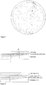
Figure 1 is a view under UV light illumination of an on-axis 4H-SiC (0001) C-face wafer cooled to 77K comprising a 7 µm thick n-type epitaxial layer. The black triangular features correspond to foreign polytype inclusions created during the epitaxial growth process. -
Figure 2 is a map of the off-axis measured on a on-axis 4H-SiC (0001) C-face substrate by high resolution X-ray diffraction, where the off-axis angle is the sum of the absolute value of the off-axis angle measured along the [1120] and the [11 00 directions. -
Figure 3 illustrates the percentage of material lost (not taking into account the slicing kerf loss) when a 25 mm thick on-axis grown SiC ingot is sliced at off-axis angles ranging from 8 to 0 degrees for ingot diameters ranging from 2 to 6 inches. -
Figure 4 is a view under UV light illumination of a 2 inch diameter 0.8° off-axis 4H-SiC (0001) C-face wafer cooled to 77K comprising a 7 µm thick n-type epitaxial layer grown according to the second embodiment of the invention. The circular darker feature in the centre of the wafer corresponds to the nitrogen doping facet introduced in the n-type underlying substrate by the crystal growth process. -
Figure 5 depicts the surface morphology under 50 times magnification of a Nomarski differential interference contrast microscope of the 7 µm thick epilayer grown on a n-type 0.8° off-axis 4H-SiC (0001) C-face wafer according to the second embodiment of the invention. The triangular defect on the left side of the picture is typical for this epilayer. -
Figure 6 is a map of the triangular defects (black squares) of the 7 µm thick epilayer of the wafer ofFigure 5 . The density of triangular defects is of 1.8 cm2 over the 2 inches wafer. -
Figure 7 is a map of the triangular defects (black squares) of a 7 um thick epilayer grown on a n-type 0.8° off-axis 4H-SiC (0001) C-face wafer with an initial growth rate for the first 0.5 µm larger than 3 µm/g at a growth temperature of 1600 °C. The density of triangular defects is of 12.3 cm-2 over the 2 inches wafer. -
Figure 8 is a cross section of a part of a bipolar device epitaxial structure comprising a substrate, a buffer layer including a boundary layer and a low doped drift layer.
The upper figure corresponds to the prior art, where the stacking fault SF can propagate from the drift layer down to intersect the substrate / boundary layer interface at location I under the active area of the device (grey region).
The lower figure shows, according to an embodiment of the invention, that when the thickness of the buffer layer is correctly adjusted to the off-axis angle of the substrate, any stacking fault which can propagate from the drift layer down to the substrate / buffer layer interface intersects this interface outside the active region of the device (open circles). -
Figure 9 illustrates the minimum thickness of the buffer layer required for the third embodiment of the invention in the case of a lcm wide power device versus the off-axis angel of the substrate upon which the epitaxial bipolar structure is grown. -
Figure 10 is a cross section of a wafer, according to an aspect of the invention, showing the boundary layer between the substrate and the device layer(s). -
Figure 3 illustrates the reduction of the material loss achieved by the invention in the case of a 25 mm long SiC ingot. Typical off-axis angles are presently 8 to 4 degrees for 2 inches and 3 inches diameter substrates, respectively. A first feature off the invention is a reduction of the off-axis angle to a value below 1 degree (e.g. 0.8 degree). Thereby, the material loss is reduced from 30 to 40% to less than 3%, respectively. The advantage of the invention become pronounced for larger diameters: in the case of 4 inches and 6 inches substrates sliced at 0.8 instead of 4 degrees, the material loss is reduced from 26 to 6% and from 41 to 9%, respectively. - The advantage of low off-axis slicing can however not be exploited in SiC devices unless homoepitaxial layers with defects densities comparable to the present state of the art can be produced. In view of the prior art, appropriate in-situ CVD etching techniques involving hydrogen and/or HCl, in combination with a growth start using a low C/Si ratio boundary layer appear as appropriate to achieve the desired result. The use of low C/Si ratios has however the disadvantage of affecting other properties of the layer, in particular its doping and the thickness uniformity. In certain cases, such as in e.g. a MESFET device structure, the thickness and doping uniformity of a moderately doped (approximately 1015 to 5×1017 cm-3) p-type layer are essential for the performances of the device, but will tend to be adversely affected by a low C/Si ratio growth.
- To overcome said limitation, the present invention proposes, as a second feature of the invention, the use of a
boundary layer 2 grown at a C/Si ratio optimized for high thickness and doping uniformity, but with a sufficiently lower supersaturation than with the followingdevice layers 3 to ensure that the epitaxial layers meets the polytype, surface defects and roughness requirements of the device. The lower supersaturation may be achieved by using, at constant growth temperature, a lower growth rate e.g. with reduced silicon and carbon precursors gas flow rates, or by the use of a higher growth temperature, or by other means suitable to the specific thin film growth process. Theboundary layer 2 can be n-type doped, not limited to but preferably above 1×1017 cm-3. Thelayer 2 can also if needed depending on targeted device structure be made p-type doped or high resistivity by introduction of intrinsic defects or doping by transition metals. This makes it possible to have theboundary layer 2 as a part of thesubstrate 1 or theepitaxial device structure 3 from an electrical (resistivity) point of view. It can also be made as an additional layer separated from thesubstrate 1 and the device layer(s)3. - According to this second feature, a typical 7 µm thick n-type Schottky diode structure was grown on a full CMP polished 0.8° off-
axis 2 inches 4H-SiC (0001)Csubstrate 1 where the growth was initiated after a gradual 3 minutes ramp of the Si- and C-gas precursors, and where the first 0.5 µm of theepitaxial structure 2 was grown at a growth rate of 1 µm/h, with a C/Si ratio of 1.2. The UV polytype map ofFig. 4 confirms the excellent replication of the 4H polytype in the epilayer with a >95% yield over the entire wafer. The surface roughness of the epilayer is 2 equivalent to the one of conventional 8° or 4° off-axis 4H-SiC (0001)Si substrates with measured RMS values of 3 to 5 nm. Epi surface defects known in the 8° or 4° off-axis prior art, such as carrots, comets, half moons etc. did not appear in this epilayer. Instead, the only surface defects detected were equilateral or isosceles shaped triangles as illustrated inFig. 5 . The defect maps ofFig. 6 , however, shows that the density of these surface defects is very low (<2 cm-2 in this experiment), a value two orders of magnitude lower than the prior art of reference [1], which illustrates the advantage of the present invention. - To confirm the influence of the growth rate at the initial stage of the epitaxial growth process, a second experiment using a CMP polished 0.8° off-
axis 2 inches 4H-SiC (0001)C substrate from the same ingot, but where the first 0.5 µm of the epitaxial structure was grown at higher Si- and C-precursor flow rates to obtain a growth rate of 3.5 µm/h, all other CVD process parameters being equal. The surface roughness of the resulting 7 µm thick n-type layers was equivalent to the one of the lower growth rate boundary layer. However, as shown inFig. 7 , the density of triangular shaped surface defects increased to 12 cm-2. This indicates that a higher defect density is obtained at C/Si ratios higher than 1 in absence of a boundary layer grown at low supersaturation. - A similar, however more pronounced effect, has been obtained by the authors of the present invention when epitaxial growth is performed on 0.8° off-
axis 2 inches 4H-SiC (0001)Si substrates. When the first 0.5 µm of 7 µm thick n-type layers were grown at growth rates higher than 3 to 4 µm/h, the 4H polytype yield was lower than 50%, whereas it was higher than 80% when the growth rate of theboundary layer 2 was less than 1.5 µm/h. - It was also observed that the surface roughness of 7 µm thick epitaxial layers grown on Si-face 4H substrates was somewhat higher than for C-face substrates loaded in the same CVD run. Further experiments showed that, the origin of this increased roughness results from a step bunching appearing on the surface of Si-face substrate during the heating stage of the CVD process, where the substrate temperature is increased from room temperature to ca. 1600 °C in presence of the hydrogen carrier gas. In order to overcome this surface degradation, the present disclosure further proposes to a) reduce the heating time to less than 30 min, b) above 1420 °C, to ramp with the temperature a Si-precursor flow scaled to 10 to 90% of the Si partial pressure above the
substrate 1 surface. This procedure may be completed with a temperature ramp of the C-precursor flow rate in order to maintain a constant C/Si ratio and will slow down the etching of the surface of thesubstrate 1, thereby reducing the step bunching prior to growth on Si-face 4H-SiC substrates. - A further feature of the present disclosure addresses the degradation phenomena in bipolar SiC devices. The prior art taught by the patent application publication
US 2003/0080842 A1 (further on designated as '80842) teaches that, in order to minimize degradation of bipolar SiC devices, a buffer layer between the substrate and the low doped drift layer shall be used, the thickness of the buffer layer being chosen so that it exceeds the diffusion length of minority carriers. As an example, a 2 µm thick n+ buffer - layer with a carrier concentration of about 2×1018 cm-3 is given for a pin structure comprising a 45 µm n- drift layer.
- This example is however in the opinion of the authors of the present invention not correct. The experimental experience shows that the diffusion length of holes in a nitrogen doped buffer layer is equivalent to the diffusion length in the drift layer, because the buffer layer's nitrogen doping alone does not reduce the minority carrier lifetime. Thus buffer layers of the order of 45 µm would be needed to practice correctly '80842. The teaching of '80842, in view of the experience of the authors of the present invention, also means that for high voltage SiC device (≥10 kV blocking voltage), buffer layers of the order of 100 µm would be needed. The approach of '80842 thus may prohibitively increase the share of the epitaxy process in the device cost structure.
- To overcome this limitation, according to a further feature of the present disclosure, it is proposed to use a buffer layer 2', the thickness of which is not chosen according to the diffusion length of he minority carriers, but is instead chosen according to the off-axis angle of the
substrate 1 upon which thebipolar device structure 3 is grown. In particular, the buffer layer 2' is, for a given off-axis angle and for a given width of the device contact along the off-axis direction, made sufficiently thick so that any basal plane defect present in thedrift layer 3 of the device does not intersect the substrate / epi interface within the contact area of the device (Figure 8 ) and thereby does not reach the substrate/epi interface where sources for SFs multiplication are expected to be present at higher density. For a typical 1×1 cm2 large power device, with a width W along the off-axis direction (e.g. [112 0]), the minimum thickness tmin of the buffer layer 2' can be calculated from the off-axis angle α by:
- As shown in
Fig. 9 , for substrates with conventional off-axis angles above 4° this approach is unrealistic due to minimum thicknesses above 500 µm. However, for off-axis angle of the order of 0.3 degrees, the minimum thickness of the buffer layer is 50 µm or less for a 1cm wide power device, which is half of the value of the estimated diffusion length of the minority carriers in a 10 kV device. It is also obvious that it becomes advantageous to use rectangular rather than square shaped contacts for a bipolar device grown on this substrate to reduce the width of the device along the off-axis direction and thus the required minimum thickness, as well as the influence per unit surface area of any staking fault propagating in to the drift layer (as the SF propagates extends along the off-axis direction). - According to still a further feature of the present disclosure, it is proposed to intentionally reduce the minority carrier lifetime in the buffer layer 2' and thus the possibility of staking faults to propagate to remaining sources of SFs multiplication within the buffer layer 2' by addition of either deep impurities in addition to the n- or p-type doping of the buffer layer 2', or alternatively by introducing intrinsic defects during epitaxial growth, or alternatively by introducing intrinsic defects acting as recombination centers by electron or proton irradiation of the buffer layer 2'.
- The teachings of the present invention can be applied to
SiC substrates 1 prepared off-axis along other planes than the (0001) plane, e.g. the {11-20} and {1-100} family planes or planes inclined between the a- and c-axis of the crystal such as the {03-38} planes of the 4H polytype. - The teachings of the present invention can be applied to other semiconductor materials having more than one polytype crystallographic structure such as GaN where the 2H hexagonal and the cubic 3C polytype can be formed.
- The epitaxial growth is performed using a Chemical Vapor Deposition (CVD) method using hydrogen (H2) as carrier gas and silane (SiH4) and a hydrocarbon gas such as ethylene (C2H4) as Si and C precursors. The CVD method is preferentially carried out in a so-called hot-wall reactor, where the wall facing the growth surface of the substrate is heated to the same temperature range as the substrate. The radial and axial temperature uniformity may be optimized to avoid nucleation of foreign polytype inclusions. The method uses preferentially a substrate temperature above 1500 °C and a reduced pressure, typically less than 250 mbar, which has the advantage of contributing to minimize the supersaturation. The so-called input C to Si ratio, the ratio of the C and Si containing precursors, is typically chosen to be less than 1.5 in the method practiced in this disclosure.
- Other Si precursors than silane may also be used such as chlorosilanes, e.g. SiH2Cl2 or SiCl4 or methylsilanes. The advantage of halogen containing precursors in respect of this invention is the well-known Si supersaturation lowering effect introduced by HCl gases. Other C precursors than ethylene may be used without loosing the teaching of the invention, e,g methane or propane.
- Thus, while there have been shown and described and pointed out fundamental novel features of the invention as applied to a preferred embodiment thereof, it will be understood that various omissions and substitutions and changes in the form and details of the devices illustrated, and in their operation, may be made by those skilled in the art. Moreover, it should be recognized that structures and/or elements and/or method steps shown and/or described in connection with any disclosed form or embodiment of the invention may be incorporated in any other disclosed or described or suggested form or embodiment as a general matter of design choice. It is the intention, therefore, to be limited only as indicated by the scope of the claims appended hereto, in which claims any reference signs shall not be construed as limiting the scope of the claims.
-
- [1] "Surface mechanisms in homoepitaxial growth on α-SiC {0001}-vicinal faces", S. Nakamura, T. Kimoto and H. Matsunami, Materials Science Forums Vols. 457-460 (2004), pp. 163-168
- [2] "Wide area homoepitaxial growth of 6H-SiC on nearly on-axis (0001) by chemical vapour deposition", S. Nakamura, T. Kimoto and H. Matsunami, Materials Science Forums Vols. 433-436 (2003), pp. 149-152
- [3] "Homoepitaxy of 6H-SiC on nearly on-axis (0001) faces by chemical vapour deposition, Part I: Effect of C/Si ratio on wide-area homoepitaxy without 3C-SiC inclusions", S. Nakamura, T. Kimoto and H. Matsunami, J. of Crystal Growth 256 (2003), p. 341-346
- [4] "Homoepitaxial on-axis growth of 4H- and 6H-SiC by CVD", C. Hallin, Q. Wahab, I. Ivanov, P. Bergman and E. Janzén, Materials Science Forums Vols. 457-460 (2004), pp. 193-196
- [5] "Challenges and first results of SiC Schottky diode manufacturing using a 3 inch technology", M. Treu, R. Rupp, H. Brunner, F. Dahlquist and C. Hecht, Materials Science Forums Vols. 457-460 (2004), pp. 981-984
- [6] "4H-SiC carbon face epitaxial layers grown by low-pressure hot-wall chemical deposition" K. Kojma, T. Takahashi, Y. Ishida, S. Kuroda, H. Oknumra and K. Arai, Materials Science Forums Vols. 457-460 (2004), pp. 209-212
- [7] "Homoepitaxial growth of 4H SiC on on-axis (0001) C-face substrates by chemical vapor deposition", K. Kojima, H. Okumura, S. Kuroda and K. Arai, J. Crystal Growth, available on-line 17-06-2004 www.sciencedirect.com
- [8] "High power SiC diodes: characteristics, reliability and relation to material defects", H. Lendemann, F. Dahlquist, J. P. Bergman, H. Bleichner and C. Hallin, Materials Science Forums 389-393 (2002) p. 1259-1264
- [9] "Recombination enhanced defect motion in forward biased 4H-SiC pn diodes", M. Skowronski, J. Q. Liu, W. M. Vetter, M. Dudley, C. Hallin and H. Lendenmann, J. Appl. Phys. 52(8) (2002), p. 4699.
- [10] "Dislocation conversion in 4H silicon carbide epitaxy", S. Ha, P. Mieszkowski, M. Skowronski and L. B. Rowland, J. of Crystal growth 244 (2002) pp. 257-266.
Claims (17)
- A method for producing, on an SiC substrate (1), SiC homoepitaxial layers (2, 3) of the same polytype as said substrate, wherein the method comprises the steps:- growing said layers (2, 3) on a surface of the SiC substrate (1), wherein said surface is inclined relative to the (0001) basal plane at an angle higher than 0.1 degree but less than 1 degree,characterized by- starting an homoepitaxial growth by forming a boundary layer (2) with a thickness up to 1 um, and- arranging, for forming said boundary layer (2), an atmosphere of lower supersaturation than with a following homoepitaxial layer (3).
- The method according to claim 1, wherein the following homoepitaxial layer is a device layer (3) or a buffer layer (2') followed by a drift layer (3).
- The method according to claim 1, further comprising the step of:- growing said boundary layer (2) with an average growth rate being less than 3 um/h.
- The method according to claim 1, further comprising the steps of:- predetermining flow rates for Silicon and Carbon precursor gases for the growth of said following homoepitaxial layer (3) and- starting said homoepitaxial growth in an atmosphere of low supersaturation by means of injecting into said atmosphere at least one of said Silicon and Carbon precursor gases at a lower flow rate than said respective predetermined flow rate for forming said boundary layer (2).
- The method according to any one of the claims 1, 3, 4, further including the steps of:- polishing, chemically and mechanically, the surface of the C-face of a substrate (1) of hexagonal polytype and- growing the homoepitaxial layer on said C-face.
- The method according to any one of claims 1, 3, 4, further including the steps of:- polishing, chemically and mechanically, the surface of the Si-face of a substrate (1) of hexagonal polytype and- growing the homoepitaxial layer on said Si-face.
- The method according to claim 5 or claim 6, including the step of:- CMP-polishing said surface to achieve a surface roughness (RMS) < 1A.
- The method according to any one of claims 1, 3, 4, further including the step of:- minimizing an etching of the growth surface during heating by introducing, above 1420 deg. C, an Si precursor gas flow scaled to the partial pressure of Si above the SiC growth surface,
- The method according to any one of claims 1, 3, 4, further including the step of:- providing said boundary layer (2) with a doping of any kind from the group of:n-type, p-type or deep levels provided by intrinsic defects or transition metals.
- The method according to any one of claims 1, 3, 4, further including the step of:- choosing the off-axis direction along any one from the group of:one of the 6 equivalent <1120> directions, one of the 6 equivalent <0110> directions.
- The method according to any one of claims 1, 3, 4, further including the step of:- choosing the off-axis direction along: between one of the equivalent <1120> directions and one of the 6 equivalent <0110> directions.
- The method according to any one of claims 1, 3, 4, further including the step of:- choosing the off-axis direction within the (0001) plane, at an angle between 10 and 20 degrees of one the equivalent <1120> directions.
- The method according to any one of claims 1, 3, 4, further including the step of:- growing a buffer layer on top of said boundary layer (2) until the thickness of said buffer layer is at least equal to the tangent of the off-axis angle between the wafer surface and the (0001) plane times the width of the device along the off-axis direction.
- The method according to any one of claims 1, 3, 4, further including the step of:- reducing minority carriers in the boundary layer (2) by introducing during epitaxial growth, or after epitaxial growth, deep levels acting as lifetime killers by means of either transition metals doping, or intrinsic in-grown defects or ex-situ generated intrinsic defects by electron or proton irradiation techniques
- Use of the wafer produced by means of the method of claim 1, characterized in that said wafer is used as a seed for growth of a SiC crystal with thickness higher than 100 microns by a sublimation or gas feed method.
- Use of the wafer produced by means of the method of claim 1, characterized in that said wafer is used for heteroepitaxial growth of nitride layers (3), such as AlN or GaN and their alloys, or oxide layers such as ZnO, on a surface of said wafer and inclined relative to the (0001) basal plane at an angle higher than 0.1 degree but less than 1 degree.
- A wafer, comprising:a SiC substrate (1) having a surface inclined relative to the (0001) basal plane at an angle higher than 0.1 degree but less than 1 degree, anda following SiC homoepitaxial layer (3) of the same polytype as the substratecharacterized by
a SiC homoepitaxial boundary layer (2) of the same polytype as the substrate, said boundary layer being arranged between the substrate and the following SiC homoepitaxial layer (3) and grown on said surface of the substrate (1) with a thickness up to 1 µm in an atmosphere of lower supersaturation than with the following SiC homoepitaxial layer (3).
Applications Claiming Priority (1)
| Application Number | Priority Date | Filing Date | Title |
|---|---|---|---|
| US58880604P | 2004-07-19 | 2004-07-19 |
Publications (3)
| Publication Number | Publication Date |
|---|---|
| EP1619276A2 EP1619276A2 (en) | 2006-01-25 |
| EP1619276A3 EP1619276A3 (en) | 2008-12-24 |
| EP1619276B1 true EP1619276B1 (en) | 2017-01-11 |
Family
ID=35295693
Family Applications (1)
| Application Number | Title | Priority Date | Filing Date |
|---|---|---|---|
| EP05014753.7A Expired - Lifetime EP1619276B1 (en) | 2004-07-19 | 2005-07-07 | Homoepitaxial growth of SiC on low off-axis SiC wafers |
Country Status (3)
| Country | Link |
|---|---|
| US (2) | US7531433B2 (en) |
| EP (1) | EP1619276B1 (en) |
| JP (1) | JP4939777B2 (en) |
Families Citing this family (90)
| Publication number | Priority date | Publication date | Assignee | Title |
|---|---|---|---|---|
| JP4238357B2 (en) * | 2003-08-19 | 2009-03-18 | 独立行政法人産業技術総合研究所 | Silicon carbide epitaxial wafer, method of manufacturing the same, and semiconductor device manufactured on the wafer |
| JP2005079339A (en) * | 2003-08-29 | 2005-03-24 | National Institute Of Advanced Industrial & Technology | Semiconductor device, and power converter, drive inverter, general-purpose inverter, and high-power high-frequency communication device using the semiconductor device |
| JPWO2005116307A1 (en) * | 2004-05-27 | 2008-04-03 | 株式会社ブリヂストン | Method for manufacturing silicon carbide single crystal wafer |
| JP2007182330A (en) * | 2004-08-24 | 2007-07-19 | Bridgestone Corp | Silicon carbide single crystal wafer and manufacturing method thereof |
| US7294324B2 (en) * | 2004-09-21 | 2007-11-13 | Cree, Inc. | Low basal plane dislocation bulk grown SiC wafers |
| JP2006321707A (en) * | 2005-04-22 | 2006-11-30 | Bridgestone Corp | Silicon carbide single crystal wafer and manufacturing method thereof |
| JP4954593B2 (en) * | 2006-04-18 | 2012-06-20 | 新日本製鐵株式会社 | Epitaxial silicon carbide single crystal substrate manufacturing method, and device using the obtained epitaxial silicon carbide single crystal substrate |
| JP4706565B2 (en) * | 2006-06-08 | 2011-06-22 | 株式会社デンソー | Method for producing silicon carbide single crystal |
| US8980445B2 (en) * | 2006-07-06 | 2015-03-17 | Cree, Inc. | One hundred millimeter SiC crystal grown on off-axis seed |
| US8432012B2 (en) | 2006-08-01 | 2013-04-30 | Cree, Inc. | Semiconductor devices including schottky diodes having overlapping doped regions and methods of fabricating same |
| US7728402B2 (en) * | 2006-08-01 | 2010-06-01 | Cree, Inc. | Semiconductor devices including schottky diodes with controlled breakdown |
| EP2631951B1 (en) * | 2006-08-17 | 2017-10-11 | Cree, Inc. | High power insulated gate bipolar transistors |
| ITMI20061809A1 (en) * | 2006-09-25 | 2008-03-26 | E T C Srl | PROCESS FOR REALIZING A SILICON CARBIDE SUSTRATE FOR MICROELECTRONIC APPLICATIONS |
| US8835987B2 (en) | 2007-02-27 | 2014-09-16 | Cree, Inc. | Insulated gate bipolar transistors including current suppressing layers |
| KR101515058B1 (en) | 2007-06-15 | 2015-04-24 | 더 리전츠 오브 더 유니버시티 오브 캘리포니아 | Planar non-polar m-plane Group-III nitride films grown on miscut substrates |
| CN101802273B (en) * | 2007-09-12 | 2013-04-17 | 昭和电工株式会社 | Epitaxial SIC single crystal substrate and method for manufacturing epitaxial SIC single crystal substrate |
| US8652255B2 (en) * | 2007-10-12 | 2014-02-18 | The United States Of America, As Represented By The Secretary Of The Navy | Method of producing epitaxial layers with low basal plane dislocation concentrations |
| JP5504597B2 (en) * | 2007-12-11 | 2014-05-28 | 住友電気工業株式会社 | Silicon carbide semiconductor device and manufacturing method thereof |
| US8221546B2 (en) * | 2008-03-26 | 2012-07-17 | Ss Sc Ip, Llc | Epitaxial growth on low degree off-axis SiC substrates and semiconductor devices made thereby |
| US8232558B2 (en) | 2008-05-21 | 2012-07-31 | Cree, Inc. | Junction barrier Schottky diodes with current surge capability |
| US8536582B2 (en) * | 2008-12-01 | 2013-09-17 | Cree, Inc. | Stable power devices on low-angle off-cut silicon carbide crystals |
| JP2010184833A (en) * | 2009-02-12 | 2010-08-26 | Denso Corp | Silicon carbide single crystal substrate and silicon carbide single crystal epitaxial wafer |
| US8294507B2 (en) | 2009-05-08 | 2012-10-23 | Cree, Inc. | Wide bandgap bipolar turn-off thyristor having non-negative temperature coefficient and related control circuits |
| US8629509B2 (en) * | 2009-06-02 | 2014-01-14 | Cree, Inc. | High voltage insulated gate bipolar transistors with minority carrier diverter |
| US8193848B2 (en) | 2009-06-02 | 2012-06-05 | Cree, Inc. | Power switching devices having controllable surge current capabilities |
| WO2010141943A1 (en) * | 2009-06-05 | 2010-12-09 | The Regents Of The University Of California | LONG WAVELENGTH NONPOLAR AND SEMIPOLAR (Al,Ga,In)N BASED LASER DIODES |
| US8541787B2 (en) * | 2009-07-15 | 2013-09-24 | Cree, Inc. | High breakdown voltage wide band-gap MOS-gated bipolar junction transistors with avalanche capability |
| US10256094B2 (en) | 2009-08-20 | 2019-04-09 | The Government Of The United States Of America, As Represented By The Secretary Of The Navy | Reduction of basal plane dislocations in epitaxial SiC using an in-situ etch process |
| US9464366B2 (en) | 2009-08-20 | 2016-10-11 | The United States Of America, As Represented By The Secretary Of The Navy | Reduction of basal plane dislocations in epitaxial SiC |
| US10256090B2 (en) | 2009-08-20 | 2019-04-09 | The United States Of America, As Represented By The Secretary Of The Navy | Reduction of basal plane dislocations in epitaxial SiC using an in-situ etch process |
| JP4959763B2 (en) | 2009-08-28 | 2012-06-27 | 昭和電工株式会社 | SiC epitaxial wafer and manufacturing method thereof |
| US8354690B2 (en) | 2009-08-31 | 2013-01-15 | Cree, Inc. | Solid-state pinch off thyristor circuits |
| JP4887418B2 (en) * | 2009-12-14 | 2012-02-29 | 昭和電工株式会社 | Method for manufacturing SiC epitaxial wafer |
| US9117739B2 (en) | 2010-03-08 | 2015-08-25 | Cree, Inc. | Semiconductor devices with heterojunction barrier regions and methods of fabricating same |
| US8415671B2 (en) | 2010-04-16 | 2013-04-09 | Cree, Inc. | Wide band-gap MOSFETs having a heterojunction under gate trenches thereof and related methods of forming such devices |
| JP4880052B2 (en) * | 2010-05-11 | 2012-02-22 | 新日本製鐵株式会社 | Epitaxial silicon carbide single crystal substrate and manufacturing method thereof |
| US8445386B2 (en) * | 2010-05-27 | 2013-05-21 | Cree, Inc. | Smoothing method for semiconductor material and wafers produced by same |
| SE1051137A1 (en) | 2010-10-29 | 2012-04-30 | Fairchild Semiconductor | Process for manufacturing a silicon carbide bipolar transistor and silicon carbide bipolar transistor thereof |
| US8927396B2 (en) * | 2010-11-17 | 2015-01-06 | Nippon Steel & Sumitomo Metal Corporation | Production process of epitaxial silicon carbide single crystal substrate |
| JP5646360B2 (en) * | 2011-02-04 | 2014-12-24 | 株式会社東芝 | Semiconductor device |
| CN103370454B (en) | 2011-04-21 | 2015-09-09 | 新日铁住金株式会社 | Epitaxial silicon carbide single crystal substrate and manufacturing method thereof |
| US9142662B2 (en) | 2011-05-06 | 2015-09-22 | Cree, Inc. | Field effect transistor devices with low source resistance |
| US9029945B2 (en) | 2011-05-06 | 2015-05-12 | Cree, Inc. | Field effect transistor devices with low source resistance |
| JP5803265B2 (en) * | 2011-05-20 | 2015-11-04 | 住友電気工業株式会社 | Silicon carbide substrate and method for manufacturing silicon carbide ingot |
| JP5961357B2 (en) * | 2011-09-09 | 2016-08-02 | 昭和電工株式会社 | SiC epitaxial wafer and manufacturing method thereof |
| US8680587B2 (en) | 2011-09-11 | 2014-03-25 | Cree, Inc. | Schottky diode |
| US8664665B2 (en) | 2011-09-11 | 2014-03-04 | Cree, Inc. | Schottky diode employing recesses for elements of junction barrier array |
| US9640617B2 (en) | 2011-09-11 | 2017-05-02 | Cree, Inc. | High performance power module |
| US9373617B2 (en) | 2011-09-11 | 2016-06-21 | Cree, Inc. | High current, low switching loss SiC power module |
| US8618582B2 (en) | 2011-09-11 | 2013-12-31 | Cree, Inc. | Edge termination structure employing recesses for edge termination elements |
| WO2013036370A1 (en) | 2011-09-11 | 2013-03-14 | Cree, Inc. | High current density power module comprising transistors with improved layout |
| JP2013089937A (en) * | 2011-10-24 | 2013-05-13 | Sumitomo Electric Ind Ltd | Method of manufacturing silicon carbide substrate, and silicon carbide substrate |
| JP6057522B2 (en) * | 2012-03-12 | 2017-01-11 | 三菱電機株式会社 | Defect inspection method |
| JP5124690B2 (en) * | 2012-03-19 | 2013-01-23 | 昭和電工株式会社 | SiC epitaxial wafer |
| CN102646578B (en) * | 2012-05-09 | 2014-09-24 | 中国电子科技集团公司第五十五研究所 | Method for Improving Batch-to-Batch Doping Uniformity of Silicon Carbide Multilayer Structure Epitaxial Material |
| US20140054609A1 (en) * | 2012-08-26 | 2014-02-27 | Cree, Inc. | Large high-quality epitaxial wafers |
| US8860040B2 (en) | 2012-09-11 | 2014-10-14 | Dow Corning Corporation | High voltage power semiconductor devices on SiC |
| US9018639B2 (en) * | 2012-10-26 | 2015-04-28 | Dow Corning Corporation | Flat SiC semiconductor substrate |
| TW201417149A (en) * | 2012-10-31 | 2014-05-01 | Lg伊諾特股份有限公司 | Epitaxial wafer |
| TW201417150A (en) * | 2012-10-31 | 2014-05-01 | Lg伊諾特股份有限公司 | Epitaxial wafer |
| JP5384714B2 (en) * | 2012-10-31 | 2014-01-08 | 昭和電工株式会社 | SiC epitaxial wafer and manufacturing method thereof |
| JP2014146748A (en) * | 2013-01-30 | 2014-08-14 | Toshiba Corp | Semiconductor device, method of manufacturing the same, and semiconductor substrate |
| US9017804B2 (en) | 2013-02-05 | 2015-04-28 | Dow Corning Corporation | Method to reduce dislocations in SiC crystal growth |
| US9797064B2 (en) | 2013-02-05 | 2017-10-24 | Dow Corning Corporation | Method for growing a SiC crystal by vapor deposition onto a seed crystal provided on a support shelf which permits thermal expansion |
| US9738991B2 (en) | 2013-02-05 | 2017-08-22 | Dow Corning Corporation | Method for growing a SiC crystal by vapor deposition onto a seed crystal provided on a supporting shelf which permits thermal expansion |
| US11721547B2 (en) * | 2013-03-14 | 2023-08-08 | Infineon Technologies Ag | Method for manufacturing a silicon carbide substrate for an electrical silicon carbide device, a silicon carbide substrate and an electrical silicon carbide device |
| US8940614B2 (en) | 2013-03-15 | 2015-01-27 | Dow Corning Corporation | SiC substrate with SiC epitaxial film |
| WO2014150400A1 (en) * | 2013-03-15 | 2014-09-25 | The Government Of The United States Of America, As Represented By The Secretary Of The Navy | Reduction of basal plane dislocations in epitaxial sic using an in-situ etch process |
| WO2015005064A1 (en) * | 2013-07-09 | 2015-01-15 | 富士電機株式会社 | Method for producing silicon carbide semiconductor device, and silicon carbide semiconductor device |
| JP5604577B2 (en) * | 2013-10-01 | 2014-10-08 | 昭和電工株式会社 | SiC epitaxial wafer |
| JP6248532B2 (en) * | 2013-10-17 | 2017-12-20 | セイコーエプソン株式会社 | 3C-SiC epitaxial layer manufacturing method, 3C-SiC epitaxial substrate, and semiconductor device |
| US9425262B2 (en) | 2014-05-29 | 2016-08-23 | Fairchild Semiconductor Corporation | Configuration of portions of a power device within a silicon carbide crystal |
| JP6479347B2 (en) * | 2014-06-06 | 2019-03-06 | ローム株式会社 | Device for manufacturing SiC epitaxial wafer, and method for manufacturing SiC epitaxial wafer |
| US9279192B2 (en) | 2014-07-29 | 2016-03-08 | Dow Corning Corporation | Method for manufacturing SiC wafer fit for integration with power device manufacturing technology |
| CN108138360B (en) * | 2015-10-07 | 2020-12-08 | 住友电气工业株式会社 | Silicon carbide epitaxial substrate and method for manufacturing silicon carbide semiconductor device |
| JP6706786B2 (en) * | 2015-10-30 | 2020-06-10 | 一般財団法人電力中央研究所 | Epitaxial wafer manufacturing method, epitaxial wafer, semiconductor device manufacturing method, and semiconductor device |
| JP6762484B2 (en) * | 2017-01-10 | 2020-09-30 | 昭和電工株式会社 | SiC epitaxial wafer and its manufacturing method |
| WO2018174105A1 (en) * | 2017-03-22 | 2018-09-27 | 東洋炭素株式会社 | Reformed sic wafer manufacturing method, epitaxial layer-attached sic wafer, method for manufacturing same, and surface processing method |
| JP7415558B2 (en) * | 2017-09-01 | 2024-01-17 | 住友電気工業株式会社 | Silicon carbide epitaxial substrate and method for manufacturing silicon carbide semiconductor device |
| JP7052322B2 (en) | 2017-11-28 | 2022-04-12 | 富士電機株式会社 | Silicon Carbide Semiconductor Device and Method for Manufacturing Silicon Carbide Semiconductor Device |
| JP7106217B2 (en) * | 2018-08-22 | 2022-07-26 | 株式会社ディスコ | Method and apparatus for detecting facet area |
| CN113122922A (en) * | 2020-06-09 | 2021-07-16 | 北京世纪金光半导体有限公司 | Seed crystal for growth of large-size silicon carbide crystal |
| IT202000016279A1 (en) * | 2020-07-06 | 2022-01-06 | St Microelectronics Srl | PROCESS FOR MANUFACTURING A SILICON CARBIDE SEMICONDUCTOR DEVICE WITH IMPROVED CHARACTERISTICS |
| EP4264672A1 (en) * | 2020-12-18 | 2023-10-25 | MI2-Factory GmbH | Electronic semiconductor component, and process for manufacturing a pretreated composite substrate for an electronic semiconductor component |
| US20220251725A1 (en) * | 2021-02-09 | 2022-08-11 | National Chung Shan Institute Of Science And Technology | Method of growing on-axis silicon carbide single crystal by regulating silicon carbide source material in size |
| JP7537446B2 (en) * | 2021-03-26 | 2024-08-21 | 株式会社プロテリアル | Silicon carbide epitaxial substrate and method for manufacturing same |
| WO2023157658A1 (en) * | 2022-02-15 | 2023-08-24 | 住友電気工業株式会社 | Silicon carbide epitaxial substrate and method for manufacturing silicon carbide semiconductor device |
| US20260082649A1 (en) * | 2022-09-13 | 2026-03-19 | Sumitomo Electric Industries, Ltd. | Silicon carbide epitaxial substrate, method of manufacturing epitaxial substrate, and method of manufacturing silicon carbide semiconductor device |
| FR3161062B1 (en) * | 2024-04-03 | 2026-02-27 | Soitec Silicon On Insulator | METHOD FOR PREPARING A COMPOSITE STRUCTURE FOR THE FABRICATION OF A HOMOEPITAXIATED SILICON CARBIDE LAYER, AND ASSOCIATED COMPOSITE STRUCTURE |
| CN119028811B (en) * | 2024-08-21 | 2025-06-20 | 天津理工大学 | A method for growing P-type 4H-SiC single crystal by PVT method |
Family Cites Families (15)
| Publication number | Priority date | Publication date | Assignee | Title |
|---|---|---|---|---|
| US5011549A (en) | 1987-10-26 | 1991-04-30 | North Carolina State University | Homoepitaxial growth of Alpha-SiC thin films and semiconductor devices fabricated thereon |
| US4912064A (en) | 1987-10-26 | 1990-03-27 | North Carolina State University | Homoepitaxial growth of alpha-SiC thin films and semiconductor devices fabricated thereon |
| JPH02283697A (en) * | 1989-04-25 | 1990-11-21 | Mitsubishi Heavy Ind Ltd | Diamond coating method and diamond coating film |
| AU2250392A (en) * | 1991-06-12 | 1993-01-12 | Case Western Reserve University | Process for the controlled growth of single-crystal films of silicon carbide polytypes on silicon carbide wafers |
| US5248385A (en) | 1991-06-12 | 1993-09-28 | The United States Of America, As Represented By The Administrator, National Aeronautics And Space Administration | Process for the homoepitaxial growth of single-crystal silicon carbide films on silicon carbide wafers |
| JPH05178698A (en) * | 1991-12-27 | 1993-07-20 | Sharp Corp | Silicon carbide bulk single crystal manufacturing apparatus and manufacturing method |
| JP3491436B2 (en) * | 1996-03-29 | 2004-01-26 | 株式会社デンソー | Method for producing silicon carbide single crystal |
| US5915194A (en) * | 1997-07-03 | 1999-06-22 | The United States Of America As Represented By The Administrator Of National Aeronautics And Space Administration | Method for growth of crystal surfaces and growth of heteroepitaxial single crystal films thereon |
| JP4185215B2 (en) * | 1999-05-07 | 2008-11-26 | 弘之 松波 | SiC wafer, SiC semiconductor device, and method of manufacturing SiC wafer |
| US6329088B1 (en) | 1999-06-24 | 2001-12-11 | Advanced Technology Materials, Inc. | Silicon carbide epitaxial layers grown on substrates offcut towards <1{overscore (1)}00> |
| US6849874B2 (en) | 2001-10-26 | 2005-02-01 | Cree, Inc. | Minimizing degradation of SiC bipolar semiconductor devices |
| US6900477B1 (en) * | 2001-12-07 | 2005-05-31 | The United States Of America As Represented By The Secretary Of The Army | Processing technique to improve the turn-off gain of a silicon carbide gate turn-off thyristor and an article of manufacture |
| JP3742877B2 (en) * | 2002-03-22 | 2006-02-08 | 独立行政法人産業技術総合研究所 | Method for producing SiC single crystal thin film |
| JP4110875B2 (en) * | 2002-08-09 | 2008-07-02 | 株式会社デンソー | Silicon carbide semiconductor device |
| JP2005079339A (en) * | 2003-08-29 | 2005-03-24 | National Institute Of Advanced Industrial & Technology | Semiconductor device, and power converter, drive inverter, general-purpose inverter, and high-power high-frequency communication device using the semiconductor device |
-
2005
- 2005-07-07 EP EP05014753.7A patent/EP1619276B1/en not_active Expired - Lifetime
- 2005-07-14 US US11/180,611 patent/US7531433B2/en not_active Expired - Lifetime
- 2005-07-19 JP JP2005208524A patent/JP4939777B2/en not_active Expired - Lifetime
-
2009
- 2009-03-12 US US12/402,551 patent/US8492772B2/en active Active
Non-Patent Citations (1)
| Title |
|---|
| None * |
Also Published As
| Publication number | Publication date |
|---|---|
| JP2006028016A (en) | 2006-02-02 |
| US20090230406A1 (en) | 2009-09-17 |
| US8492772B2 (en) | 2013-07-23 |
| US20060011128A1 (en) | 2006-01-19 |
| EP1619276A2 (en) | 2006-01-25 |
| JP4939777B2 (en) | 2012-05-30 |
| EP1619276A3 (en) | 2008-12-24 |
| US7531433B2 (en) | 2009-05-12 |
Similar Documents
| Publication | Publication Date | Title |
|---|---|---|
| US8492772B2 (en) | Homoepitaxial growth of SiC on low off-axis SiC wafers | |
| US5915194A (en) | Method for growth of crystal surfaces and growth of heteroepitaxial single crystal films thereon | |
| US6165874A (en) | Method for growth of crystal surfaces and growth of heteroepitaxial single crystal films thereon | |
| EP0609799B1 (en) | Improvements in heteroepitaxy by large surface steps | |
| US5463978A (en) | Compound semiconductor and controlled doping thereof | |
| EP2192211B1 (en) | Stable Power Devices on Low-Angle Off-Cut Silicon Carbide Crystals | |
| US5709745A (en) | Compound semi-conductors and controlled doping thereof | |
| Kojima et al. | Homoepitaxial growth of 4H-SiC on on-axis (0001) C-face substrates by chemical vapor depositon | |
| US8591651B2 (en) | Epitaxial growth on low degree off-axis silicon carbide substrates and semiconductor devices made thereby | |
| US6488771B1 (en) | Method for growing low-defect single crystal heteroepitaxial films | |
| US20200056302A1 (en) | Elimination of Basal Plane Dislocation and Pinning the Conversion Point Below the Epilayer Interface for SiC Power Device Applications | |
| US20080318359A1 (en) | Method of manufacturing silicon carbide semiconductor substrate | |
| WO1992022922A2 (en) | Process for the controlled growth of single-crystal films of silicon carbide polytypes on silicon carbide wafers | |
| WO2009048997A1 (en) | Producing epitaxial layers with low basal plane dislocation concentrations | |
| JP7647791B2 (en) | SiC epitaxial wafer | |
| US6461944B2 (en) | Methods for growth of relatively large step-free SiC crystal surfaces | |
| Masumoto et al. | The growth of 3-inch 4H-SiC Si-face epitaxial wafer with vicinal off-angle | |
| Kojima et al. | Reducing the wafer off angle for 4H-SiC homoepitaxy | |
| WO2025188374A2 (en) | N-polar iii-nitride semiconductors on silicon carbide | |
| Bhat | Epitaxial Growth of Silicon Carbide by Chemical Vapor Deposition | |
| Henry et al. | Epitaxial growth on on-axis substrates | |
| Bergman et al. | Improved SiC Epitaxial Material for Bipolar Applications | |
| ul Hassan et al. | On-axis Homoepitaxy on Full 2” 4H-SiC Wafer for High Power Applications | |
| Kimoto et al. | Epitaxial Growth and Characterization of 4H-SiC (11–20) and (03–38) | |
| Lee | 4H-SiC Homoepitaxial Growth on Various SiC Substrates for Power Device Application |
Legal Events
| Date | Code | Title | Description |
|---|---|---|---|
| PUAI | Public reference made under article 153(3) epc to a published international application that has entered the european phase |
Free format text: ORIGINAL CODE: 0009012 |
|
| AK | Designated contracting states |
Kind code of ref document: A2 Designated state(s): AT BE BG CH CY CZ DE DK EE ES FI FR GB GR HU IE IS IT LI LT LU LV MC NL PL PT RO SE SI SK TR |
|
| AX | Request for extension of the european patent |
Extension state: AL BA HR MK YU |
|
| PUAL | Search report despatched |
Free format text: ORIGINAL CODE: 0009013 |
|
| AK | Designated contracting states |
Kind code of ref document: A3 Designated state(s): AT BE BG CH CY CZ DE DK EE ES FI FR GB GR HU IE IS IT LI LT LU LV MC NL PL PT RO SE SI SK TR |
|
| AX | Request for extension of the european patent |
Extension state: AL BA HR MK YU |
|
| 17P | Request for examination filed |
Effective date: 20090624 |
|
| AKX | Designation fees paid |
Designated state(s): AT BE BG CH CY CZ DE DK EE ES FI FR GB GR HU IE IS IT LI LT LU LV MC NL PL PT RO SE SI SK TR |
|
| 17Q | First examination report despatched |
Effective date: 20090923 |
|
| RIC1 | Information provided on ipc code assigned before grant |
Ipc: H01L 21/02 20060101ALI20151023BHEP Ipc: C30B 25/20 20060101ALI20151023BHEP Ipc: C30B 29/36 20060101AFI20151023BHEP Ipc: C30B 25/02 20060101ALI20151023BHEP Ipc: C30B 25/18 20060101ALI20151023BHEP |
|
| GRAP | Despatch of communication of intention to grant a patent |
Free format text: ORIGINAL CODE: EPIDOSNIGR1 |
|
| INTG | Intention to grant announced |
Effective date: 20160921 |
|
| GRAS | Grant fee paid |
Free format text: ORIGINAL CODE: EPIDOSNIGR3 |
|
| STAA | Information on the status of an ep patent application or granted ep patent |
Free format text: STATUS: GRANT OF PATENT IS INTENDED |
|
| GRAA | (expected) grant |
Free format text: ORIGINAL CODE: 0009210 |
|
| STAA | Information on the status of an ep patent application or granted ep patent |
Free format text: STATUS: THE PATENT HAS BEEN GRANTED |
|
| AK | Designated contracting states |
Kind code of ref document: B1 Designated state(s): AT BE BG CH CY CZ DE DK EE ES FI FR GB GR HU IE IS IT LI LT LU LV MC NL PL PT RO SE SI SK TR |
|
| REG | Reference to a national code |
Ref country code: GB Ref legal event code: FG4D |
|
| REG | Reference to a national code |
Ref country code: CH Ref legal event code: EP |
|
| REG | Reference to a national code |
Ref country code: AT Ref legal event code: REF Ref document number: 861368 Country of ref document: AT Kind code of ref document: T Effective date: 20170115 |
|
| REG | Reference to a national code |
Ref country code: IE Ref legal event code: FG4D |
|
| REG | Reference to a national code |
Ref country code: DE Ref legal event code: R096 Ref document number: 602005051117 Country of ref document: DE |
|
| REG | Reference to a national code |
Ref country code: SE Ref legal event code: TRGR |
|
| REG | Reference to a national code |
Ref country code: LT Ref legal event code: MG4D |
|
| REG | Reference to a national code |
Ref country code: NL Ref legal event code: MP Effective date: 20170111 |
|
| PG25 | Lapsed in a contracting state [announced via postgrant information from national office to epo] |
Ref country code: NL Free format text: LAPSE BECAUSE OF FAILURE TO SUBMIT A TRANSLATION OF THE DESCRIPTION OR TO PAY THE FEE WITHIN THE PRESCRIBED TIME-LIMIT Effective date: 20170111 |
|
| PG25 | Lapsed in a contracting state [announced via postgrant information from national office to epo] |
Ref country code: LT Free format text: LAPSE BECAUSE OF FAILURE TO SUBMIT A TRANSLATION OF THE DESCRIPTION OR TO PAY THE FEE WITHIN THE PRESCRIBED TIME-LIMIT Effective date: 20170111 Ref country code: IS Free format text: LAPSE BECAUSE OF FAILURE TO SUBMIT A TRANSLATION OF THE DESCRIPTION OR TO PAY THE FEE WITHIN THE PRESCRIBED TIME-LIMIT Effective date: 20170511 Ref country code: GR Free format text: LAPSE BECAUSE OF FAILURE TO SUBMIT A TRANSLATION OF THE DESCRIPTION OR TO PAY THE FEE WITHIN THE PRESCRIBED TIME-LIMIT Effective date: 20170412 Ref country code: FI Free format text: LAPSE BECAUSE OF FAILURE TO SUBMIT A TRANSLATION OF THE DESCRIPTION OR TO PAY THE FEE WITHIN THE PRESCRIBED TIME-LIMIT Effective date: 20170111 |
|
| PG25 | Lapsed in a contracting state [announced via postgrant information from national office to epo] |
Ref country code: PT Free format text: LAPSE BECAUSE OF FAILURE TO SUBMIT A TRANSLATION OF THE DESCRIPTION OR TO PAY THE FEE WITHIN THE PRESCRIBED TIME-LIMIT Effective date: 20170511 Ref country code: PL Free format text: LAPSE BECAUSE OF FAILURE TO SUBMIT A TRANSLATION OF THE DESCRIPTION OR TO PAY THE FEE WITHIN THE PRESCRIBED TIME-LIMIT Effective date: 20170111 Ref country code: ES Free format text: LAPSE BECAUSE OF FAILURE TO SUBMIT A TRANSLATION OF THE DESCRIPTION OR TO PAY THE FEE WITHIN THE PRESCRIBED TIME-LIMIT Effective date: 20170111 Ref country code: BG Free format text: LAPSE BECAUSE OF FAILURE TO SUBMIT A TRANSLATION OF THE DESCRIPTION OR TO PAY THE FEE WITHIN THE PRESCRIBED TIME-LIMIT Effective date: 20170411 Ref country code: LV Free format text: LAPSE BECAUSE OF FAILURE TO SUBMIT A TRANSLATION OF THE DESCRIPTION OR TO PAY THE FEE WITHIN THE PRESCRIBED TIME-LIMIT Effective date: 20170111 |
|
| REG | Reference to a national code |
Ref country code: DE Ref legal event code: R097 Ref document number: 602005051117 Country of ref document: DE |
|
| PG25 | Lapsed in a contracting state [announced via postgrant information from national office to epo] |
Ref country code: EE Free format text: LAPSE BECAUSE OF FAILURE TO SUBMIT A TRANSLATION OF THE DESCRIPTION OR TO PAY THE FEE WITHIN THE PRESCRIBED TIME-LIMIT Effective date: 20170111 Ref country code: RO Free format text: LAPSE BECAUSE OF FAILURE TO SUBMIT A TRANSLATION OF THE DESCRIPTION OR TO PAY THE FEE WITHIN THE PRESCRIBED TIME-LIMIT Effective date: 20170111 Ref country code: SK Free format text: LAPSE BECAUSE OF FAILURE TO SUBMIT A TRANSLATION OF THE DESCRIPTION OR TO PAY THE FEE WITHIN THE PRESCRIBED TIME-LIMIT Effective date: 20170111 Ref country code: CZ Free format text: LAPSE BECAUSE OF FAILURE TO SUBMIT A TRANSLATION OF THE DESCRIPTION OR TO PAY THE FEE WITHIN THE PRESCRIBED TIME-LIMIT Effective date: 20170111 |
|
| PLBE | No opposition filed within time limit |
Free format text: ORIGINAL CODE: 0009261 |
|
| STAA | Information on the status of an ep patent application or granted ep patent |
Free format text: STATUS: NO OPPOSITION FILED WITHIN TIME LIMIT |
|
| PG25 | Lapsed in a contracting state [announced via postgrant information from national office to epo] |
Ref country code: DK Free format text: LAPSE BECAUSE OF FAILURE TO SUBMIT A TRANSLATION OF THE DESCRIPTION OR TO PAY THE FEE WITHIN THE PRESCRIBED TIME-LIMIT Effective date: 20170111 |
|
| 26N | No opposition filed |
Effective date: 20171012 |
|
| PG25 | Lapsed in a contracting state [announced via postgrant information from national office to epo] |
Ref country code: SI Free format text: LAPSE BECAUSE OF FAILURE TO SUBMIT A TRANSLATION OF THE DESCRIPTION OR TO PAY THE FEE WITHIN THE PRESCRIBED TIME-LIMIT Effective date: 20170111 |
|
| REG | Reference to a national code |
Ref country code: CH Ref legal event code: PL |
|
| GBPC | Gb: european patent ceased through non-payment of renewal fee |
Effective date: 20170707 |
|
| REG | Reference to a national code |
Ref country code: IE Ref legal event code: MM4A |
|
| REG | Reference to a national code |
Ref country code: FR Ref legal event code: ST Effective date: 20180330 |
|
| PG25 | Lapsed in a contracting state [announced via postgrant information from national office to epo] |
Ref country code: CH Free format text: LAPSE BECAUSE OF NON-PAYMENT OF DUE FEES Effective date: 20170731 Ref country code: GB Free format text: LAPSE BECAUSE OF NON-PAYMENT OF DUE FEES Effective date: 20170707 Ref country code: IE Free format text: LAPSE BECAUSE OF NON-PAYMENT OF DUE FEES Effective date: 20170707 Ref country code: LI Free format text: LAPSE BECAUSE OF NON-PAYMENT OF DUE FEES Effective date: 20170731 |
|
| PG25 | Lapsed in a contracting state [announced via postgrant information from national office to epo] |
Ref country code: FR Free format text: LAPSE BECAUSE OF NON-PAYMENT OF DUE FEES Effective date: 20170731 |
|
| REG | Reference to a national code |
Ref country code: BE Ref legal event code: MM Effective date: 20170731 |
|
| PG25 | Lapsed in a contracting state [announced via postgrant information from national office to epo] |
Ref country code: LU Free format text: LAPSE BECAUSE OF NON-PAYMENT OF DUE FEES Effective date: 20170707 |
|
| PG25 | Lapsed in a contracting state [announced via postgrant information from national office to epo] |
Ref country code: BE Free format text: LAPSE BECAUSE OF NON-PAYMENT OF DUE FEES Effective date: 20170731 |
|
| REG | Reference to a national code |
Ref country code: AT Ref legal event code: UEP Ref document number: 861368 Country of ref document: AT Kind code of ref document: T Effective date: 20170111 |
|
| PG25 | Lapsed in a contracting state [announced via postgrant information from national office to epo] |
Ref country code: HU Free format text: LAPSE BECAUSE OF FAILURE TO SUBMIT A TRANSLATION OF THE DESCRIPTION OR TO PAY THE FEE WITHIN THE PRESCRIBED TIME-LIMIT; INVALID AB INITIO Effective date: 20050707 Ref country code: MC Free format text: LAPSE BECAUSE OF FAILURE TO SUBMIT A TRANSLATION OF THE DESCRIPTION OR TO PAY THE FEE WITHIN THE PRESCRIBED TIME-LIMIT Effective date: 20170111 |
|
| PG25 | Lapsed in a contracting state [announced via postgrant information from national office to epo] |
Ref country code: CY Free format text: LAPSE BECAUSE OF NON-PAYMENT OF DUE FEES Effective date: 20170111 |
|
| PG25 | Lapsed in a contracting state [announced via postgrant information from national office to epo] |
Ref country code: TR Free format text: LAPSE BECAUSE OF FAILURE TO SUBMIT A TRANSLATION OF THE DESCRIPTION OR TO PAY THE FEE WITHIN THE PRESCRIBED TIME-LIMIT Effective date: 20170111 |
|
| PGFP | Annual fee paid to national office [announced via postgrant information from national office to epo] |
Ref country code: IT Payment date: 20200622 Year of fee payment: 16 |
|
| PG25 | Lapsed in a contracting state [announced via postgrant information from national office to epo] |
Ref country code: IT Free format text: LAPSE BECAUSE OF NON-PAYMENT OF DUE FEES Effective date: 20210707 |
|
| PGFP | Annual fee paid to national office [announced via postgrant information from national office to epo] |
Ref country code: SE Payment date: 20240619 Year of fee payment: 20 |
|
| PGFP | Annual fee paid to national office [announced via postgrant information from national office to epo] |
Ref country code: DE Payment date: 20240619 Year of fee payment: 20 |
|
| PGFP | Annual fee paid to national office [announced via postgrant information from national office to epo] |
Ref country code: AT Payment date: 20240620 Year of fee payment: 20 |
|
| REG | Reference to a national code |
Ref country code: DE Ref legal event code: R071 Ref document number: 602005051117 Country of ref document: DE |
|
| REG | Reference to a national code |
Ref country code: SE Ref legal event code: EUG |