EP1617468A1 - Probe apparatus with optical length-measuring unit and probe testing method - Google Patents
Probe apparatus with optical length-measuring unit and probe testing method Download PDFInfo
- Publication number
- EP1617468A1 EP1617468A1 EP04702857A EP04702857A EP1617468A1 EP 1617468 A1 EP1617468 A1 EP 1617468A1 EP 04702857 A EP04702857 A EP 04702857A EP 04702857 A EP04702857 A EP 04702857A EP 1617468 A1 EP1617468 A1 EP 1617468A1
- Authority
- EP
- European Patent Office
- Prior art keywords
- measuring unit
- optical length
- probe
- susceptor
- directional
- Prior art date
- Legal status (The legal status is an assumption and is not a legal conclusion. Google has not performed a legal analysis and makes no representation as to the accuracy of the status listed.)
- Ceased
Links
Images



Classifications
-
- G—PHYSICS
- G01—MEASURING; TESTING
- G01R—MEASURING ELECTRIC VARIABLES; MEASURING MAGNETIC VARIABLES
- G01R31/00—Arrangements for testing electric properties; Arrangements for locating electric faults; Arrangements for electrical testing characterised by what is being tested not provided for elsewhere
- G01R31/28—Testing of electronic circuits, e.g. by signal tracer
- G01R31/2851—Testing of integrated circuits [IC]
- G01R31/2886—Features relating to contacting the IC under test, e.g. probe heads; chucks
- G01R31/2891—Features relating to contacting the IC under test, e.g. probe heads; chucks related to sensing or controlling of force, position, temperature
-
- H—ELECTRICITY
- H10—SEMICONDUCTOR DEVICES; ELECTRIC SOLID-STATE DEVICES NOT OTHERWISE PROVIDED FOR
- H10P—GENERIC PROCESSES OR APPARATUS FOR THE MANUFACTURE OR TREATMENT OF DEVICES COVERED BY CLASS H10
- H10P74/00—Testing or measuring during manufacture or treatment of wafers, substrates or devices
-
- G—PHYSICS
- G01—MEASURING; TESTING
- G01R—MEASURING ELECTRIC VARIABLES; MEASURING MAGNETIC VARIABLES
- G01R31/00—Arrangements for testing electric properties; Arrangements for locating electric faults; Arrangements for electrical testing characterised by what is being tested not provided for elsewhere
- G01R31/28—Testing of electronic circuits, e.g. by signal tracer
- G01R31/2851—Testing of integrated circuits [IC]
- G01R31/2886—Features relating to contacting the IC under test, e.g. probe heads; chucks
- G01R31/2887—Features relating to contacting the IC under test, e.g. probe heads; chucks involving moving the probe head or the IC under test; docking stations
Definitions
- FIG. 6 shows a second embodiment of the invention.
- the second embodiment comprises, as well as the elements of the probe apparatus of the firsts embodiment, a second optical length-measuring unit 5 for detecting a change in the Z-directional position of the probe card 14. Since the other elements of the second embodiment are similar to those of the first embodiment, only the second optical length-measuring unit 5 will be described.
- the second optical length-measuring unit 5 may be similar to the first optical length-measuring unit 4, and may incorporate a second irradiator 5a and second detector 5b.
Landscapes
- Engineering & Computer Science (AREA)
- Computer Hardware Design (AREA)
- Microelectronics & Electronic Packaging (AREA)
- General Engineering & Computer Science (AREA)
- Physics & Mathematics (AREA)
- General Physics & Mathematics (AREA)
- Testing Or Measuring Of Semiconductors Or The Like (AREA)
- Measuring Leads Or Probes (AREA)
- Tests Of Electronic Circuits (AREA)
Abstract
Description
- This application is based upon and claims the benefit of priority from prior Japanese Patent Application No. 2003-011140, filed January 20, 2003, the entire contents of which are incorporated herein by reference.
- The present invention relates to a probe apparatus and probe testing method for testing the electrical characteristic of a plurality of to-be-tested objects (hereinafter referred to as "chips") provided on a substrate (hereinafter referred to as a "wafer") W. More particularly, it relates to a probe apparatus that includes detection means for directly detecting the position of each chip and the position of a probe card, and a probe testing method.
- To detect the position of a chip, it is necessary to align the X-, Y-, Z- and θ-directional positions of the probes of a probe card with those of the chip, and to raise the chip toward the probes to bring it into accurate contact with the probes with a predetermined overdrive amount. To this end, it is necessary to accurately detect the position of the chip. Since the foundation layers of the electrode sections or electrodes of recent chips are thin and soft, excessive overdrive may damage, expose and/or crack the foundation layers. To achieve such alignment, each electrode of a chip and the tip of each probe have been photographed by a camera to detect their positions. The detection of the X-, Y-, Z- and θ-directional positions using a camera can be performed highly accurately, and is therefore widely utilized. However, in Z-directional positioning using a camera, the camera is focused on a target, and the distance therebetween is measured. Accordingly, this method is disadvantageous, for example, in that the range of distances that can be measured is narrow, and the detection accuracy is low. A detection error, if there is any, adversely influences the contact pressure between the probes and the chip. As a result, the probes and chip may be damaged, or the probes may not satisfactorily contact the chip to cause a characteristic detection error. Jpn. Pat. Appln. KOKAI Publication No. 11-26524 discloses an apparatus for performing Z-directional positioning of probes and a chip using optical length-measuring units. Although the apparatus disclosed in this publication has two optical length-measuring units, it cannot directly detect the positions of the probes and the chip. Further, it is necessary to move a main chuck to a predetermined position for position detection. It is also necessary to perform focusing of a camera during position detection, and to measure the distance between the probes and the chip from the focal point. Therefore, much time is required for position detection, and accurate position detection cannot be achieved.
- In accordance with an aspect, the invention provides a probe apparatus capable of reducing a detection error using a simple structure, and appropriately controlling the overdrive amount to further enhance the reliability of tests, and a probe testing method for enabling such control.
- In accordance with another aspect, the invention provides a probe apparatus capable of detecting a change in Z-directional position due to deformation of a probe card, thereby performing more accurate positioning of a chip and probes, and a probe testing method for enabling such accurate positioning.
- In accordance with a first aspect of the invention, there is provided a probe apparatus for testing an electrical characteristic of a to-be-tested object formed on a substrate W.
- The probe apparatus comprises: a prober chamber; a susceptor provided in the prober chamber and configured to place thereon a substrate with a plurality of to-be-tested objects formed; a probe card provided in the prober chamber (the probe card includes a plurality of probes and opposes the susceptor); and a first optical length-measuring unit (the first optical length-measuring unit emits light to the surface of each to-be-tested object placed on the susceptor, detects the position, on the light-receiving surface of the first optical length-measuring unit, of light reflected from the each to-be-tested object, and detects the Z-directional position of the each to-be-tested object based on the detected position of light reflected).
- The probe apparatus of the invention according to the first aspect may include one or several of the following preferable structures (1) to (12):
- (1) A reference plane is attached to the susceptor, the reference plane being referred to when the first optical length-measuring unit detects the Z-directional position.
- (2) The light emitted from the first optical length-measuring unit is a laser beam.
- (3) The laser beam has a diameter of 10 to 30 µm.
- (4) The first optical length-measuring unit is attached to one of an upper wall and a sidewall of the prober chamber.
- (5) A moving mechanism for moving the susceptor in a Z-direction, and a control unit for controlling the moving mechanism are also provided. The first optical length-measuring unit detects the Z-directional positions of a plurality of surface portions of one of the susceptor and the substrate placed on the susceptor. Further, the control unit creates a map concerning the Z-directional positions of the plurality of surface portions, based on the Z-directional positions of the plurality of surface portions detected by the first optical length-measuring unit.
- (6) A second optical length-measuring unit emits light to the surface of a support member supporting the probe card, detects the position, on the light-receiving surface of the second optical length-measuring unit, of light reflected from the support member, and detects the Z-directional position of the probe card based on the detected position of light reflected.
- (7) The light emitted from the second optical length-measuring unit is a laser beam.
- (8) A holding plate is also provided (the holding plate is located above the probe card), and the second optical length-measuring unit is attached to the surface of the holding plate opposing the probe card.
- (9) A probe-card support member supporting the probe card is also provided (the probe-card support member is attached to the upper surface of the probe card), and the second optical length-measuring unit detects the upper surface of the probe-card support member to detect a change in the Z-directional position of the probe card.
- (10) The probe-card support member includes a reflector provided on a portion thereof to be detected by the second optical length-measuring unit, the reflector reflecting the emitted light.
- (11) The second optical length-measuring unit detects a side surface of the probe card to detect a change in the Z-directional position of the probe card.
- (12) The probe card includes an optical element provided on a side surface thereof to be detected by the second optical length-measuring unit, the optical element reflecting the emitted light.
In accordance with a second aspect of the invention, there is provided a method of testing a to-be-tested object using the probe apparatus provided with the structure (1). The method comprises:- (a) placing the substrate on the susceptor; (b) (b1) detecting the Z-directional position of the reference plane attached to the susceptor, using the first optical length-measuring unit; (b2) raising the susceptor and bringing the reference plane into contact with the probes to measure the distance between the reference plane and the probes; (c) detecting the Z-directional position of the to-be-tested object, using the first optical length-measuring unit; (d) measuring the distance between the surface of the to-be-tested object and the tips of the probes based on results of the (b) and (c); (e) raising the susceptor in a Z-direction to bring the to-be-tested object into contact with the probes, using a moving mechanism based on the distance between the to-be-tested object and the probes measured in the (d); (f) measuring the electrical characteristic of the to-be-tested object; and (g) moving the substrate by a measuring pitch corresponding to one to-be-tested object, repeating the (e) to (f) to detect the position of a next to-be-tested object.
It is preferable that the above method includes one of several of the following features (13) and (14): - (13) (c1) The Z-directional positions of a plurality of surface portions of the substrate are detected using the first optical length-measuring unit.
- (c2) A map concerning the detected Z-directional positions of the plurality of surface portions of the substrate is created.
- (c3) Based on the map created in the (c2), the susceptor is moved in the Z-direction to bring the to-be-tested object into contact with the probes, using the moving mechanism.
- (14) (a2) After the (a), a second optical length-measuring unit emits light to the upper surface of a support member supporting the probe card, detects the position, on the light-receiving surface of the second optical length-measuring unit, of light reflected from the support member, and detects the Z-directional position of the probe card based on the detected position of light reflected.
- The (d) includes measuring the distance between the to-be-tested object and the probes, based on the detection result acquired in the (a2) in addition to the detection results acquired in the (b) and (c).
- The invention can be applied to a probe apparatus and probe testing method for measuring the electrical characteristic of a to-be-tested object (e.g., a semiconductor device) provided on a wafer.
-
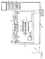
- FIG. 1 is a sectional view of a probe apparatus according to a first embodiment;
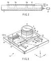
- FIG. 2 is a view of an example of a substrate-
fixing mechanism 23 employed in each embodiment of the invention; - FIG. 3 is a view of an example of a
moving mechanism 16 employed in each embodiment of the invention; - FIG. 4 is a view illustrating the principle of an optical length-measuring unit for use in each embodiment;
- FIG. 5 is a view illustrating an example of a map used in each embodiment, in which a wafer W is divided into zones;
- FIG. 6 is a sectional view of a probe apparatus according to a second embodiment;
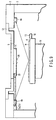
- FIG. 7 is an enlarged view illustrating an essential part of the probe apparatus of the second embodiment;
- FIG. 8 is a sectional view of a probe apparatus according to a third embodiment; and
- FIG. 9 is an enlarged view illustrating an essential part of the probe apparatus of the third embodiment.
- Referring to several drawings, a first embodiment of the invention will be described. FIG. 1 is a sectional view illustrating the main unit of a
probe apparatus 100 according to the first embodiment of the invention. Theprobe apparatus 100 of the embodiment has aprober chamber 29. Theprober chamber 29 has anupper wall 2 andsidewalls 3. Theupper wall 2 may have anopening 7 at the center. The prober chamber contains asusceptor 6 for placing thereon a substrate (hereinafter referred to simply as a "wafer") W. Thesusceptor 6 is mounted on a movingmechanism 16. The movingmechanism 16 moves the susceptor in the X-, Y-, Z- and θ-directions. The movingmechanism 16 is controlled by acontrol unit 17. - The
susceptor 6 may have a substrate-fixingmechanism 23 for holding a wafer W placed thereon. FIG. 2 shows an example of the substrate-fixingmechanism 23. The substrate-fixingmechanism 23 includes, for example,grooves 23a formed in the surface of the susceptor, and a air charging/discharginghole 23b connected to thegrooves 23a. When avacuum pump 22 removes by suction air from thegrooves 23a via thehole 23b, the wafer W is fixed on the surface of the substrate-fixingmechanism 23. The substrate-fixingmechanism 23 can employ, as well as the vacuum suction mechanism, a holding mechanism utilizing static electricity, or a mechanical holding mechanism. - FIG. 3 shows an example of the moving
mechanism 16 for moving thesusceptor 6. The movingmechanism 16 comprises thesusceptor 6 with the wafer W placed thereon, an X-stage 30 for supporting thesusceptor 6, a Y-stage 32 for supporting the X-stage, and a base table 34 for supporting these. When the electrical characteristics of the wafer W is tested, thesusceptor 6 is moved in the X- and Y-directions by the X- and Y-stages 30 and 32, and is vertically moved in the Z-direction by avertical driving mechanism 6a provided as the lower portion of thesusceptor 6. The X-stage 30 is reciprocated on the Y-stage 32 by anX-directional driving mechanism 41 along X-directional rails 31. The Y-stage 32 is reciprocated on the base stable 34 by a Y-directional driving mechanism 42 along Y-directional rails 33. The X- and Y-directional driving mechanisms motors vertical driving mechanism 6a may be formed of, for example, a motor, a ball screw rotated in opposite directions by the motor, and a nut member engaged with the ball screw and fixed to the susceptor. By rotating the ball screw by the motor, thesusceptor 6 is vertically moved via the nut member. Further, thesusceptor 6 includes a θ-directional rotation mechanism 6b. The θ-directional rotation mechanism 6b rotates thesusceptor 6. - The moving mechanism that can be employed in the invention is not limited to that shown in FIG. 3, but may be any type of moving mechanism if it can rotate the susceptor in the X-, Y-, Z- and θ-directions.
- In FIG. 1, in the
opening 7 formed in the upper portion of theprober chamber 29, aprobe card 14 is opposed to thesusceptor 6. Theprobe card 14 has a plurality ofprobes 26 for testing the electrical characteristic of eachchip 1 formed on the wafer W. Theprobe card 14 may be attached to, for example, the lower surface of a probe-card support member 9. The probe-card support member 9 may be directly attached to theupper wall 2, or be detachably attached to ahead plate 12 fitted in theopening 7 of theupper wall 2. - Further, the
prober chamber 29 contains upper andlower cameras chip 1 and theprobe 26. Thelower camera 15b may be placed near thesusceptor 6, while theupper camera 15a may be placed at an upper position in theprober chamber 29. Theupper camera 15a is attached to, for example, the longitudinally central portion of analignment bridge 15d located in the X-direction. Thealignment bridge 15d can be reciprocated in the Y-direction alongguide rails 15c provided on the upper portions of the sidewalls of the prober chamber. - The
lower camera 15b photographs the tips of theprobes 26 of theprobe card 14, and theupper camera 15a photographs the electrodes of eachchip 1 formed on the wafer W. Based on the coordinate positions of the photographed members, thecontrol unit 17 calculates the positional relationship between the electrodes of eachchip 1 and the tips of theprobes 26, thereby moving thesusceptor 6 to align eachchip 1 with theprobe 26. - To align the Z-directional positions of each
chip 1 and theprobes 26, the first embodiment of the invention employs a first optical length-measuring unit 4 (4a, 4b). The first optical length-measuring unit 4 can emit light to the surface of eachchip 1 formed on the wafer W that is placed on thesusceptor 6, detect the position, on a light-receiving surface thereof, of light reflected from each chip, and directly and accurately detect the Z-directional position of eachchip 1 based on the detected position of light reflected. The first optical length-measuring unit 4 can be provided at any position in theprober chamber 29. However, if, in particular, it is provided on theupper wall 2 or on the upper portion of thesidewall 3, it can perform accurate position detection with little blurring. - The first optical length-measuring unit 4 includes a
first irradiator 4a andfirst detector 4b. Light emitted from thefirst irradiator 4a reflects from a to-be-measured object, such as thechip 1, and enters thefirst detector 4b. At this time, if the Z-directional position of the plane that reflects the light is changed, the incident position of the light on the detector is shifted. Based on the shift amount of the light, the Z-directional position of the plane that reflects the light can be detected. FIG. 4 is a view illustrating the principle of measurement. When areflection plane 20 is positioned at position A, light reflects from point A'. When the reflection plane is positioned at position B, light reflects from point B'. These reflected light beams enter points A" and B" on anincident plane 21. Assume here that a change in the position of a point from which light reflects is ΔX, a change in the Z-directional position of the reflection plane is ΔZ, the magnitude of an optical system, through which light from thereflection plane 20 enters the incident plane, is M, and the angle of incidence of light entering the reflection plane is θ. Further, assume that the distance between points A" and B" on the incident plane is Δmeas, from point A" to point B" the incident position of light on the incident plane being shifted when the reflection plane is changed from A to B. In this case, the following equations are established:

- From (1) and (2),

- Since 2 x M x tan θ is a constant, if it is substituted by K, ΔZ is given by

- From this, it is understood that ΔZ can be determined if Δ meas is measured.
- The use of the optical length-measuring unit enables even a slight change in the position of a reflection plane to be detected, and hence can realize more accurate position detection than the conventional position detection method utilizing the focus of a camera. Further, in the position detection utilizing the focus of a camera, it is necessary to vertically move the
susceptor 6 to focus a camera on thechip 1, with the result that much time is required for position detection. In contrast, in the optical length-measuring unit, if a to-be-measured object, i.e., thechip 1, is positioned in a detection range, the position of the object can be detected without vertically moving the susceptor, thereby significantly reducing the time required for the position detection. Furthermore, the Z-directional detectable range of the optical length-measuring unit is 200 µm, which is wider than that of the method utilizing the focus of a camera. Namely, position detection can be more easily performed. The Z-directional detectable range of the optical length-measuring unit can be further widened if a longer length-measuring sensor is used. - In the first embodiment of the invention, since the surface of the wafer W, i.e., the
chip 1, can be directly detected by a single optical length-measuring unit, the probe apparatus can be made to a simple structure, and detection errors in the length-measuring unit can be reduced to thereby enhance the detection accuracy. Further, where a mechanism that performs detection based on a change in the position of incident light on a detector, not based on the amount of reflected light, like the optical length-measuring unit of the embodiment, is employed, reliable detection results can be acquired regardless of the state of the reflection plane. Furthermore, since the first optical length-measuring unit 4 used in the embodiment can detect the position of a target even at a far distance, it may be placed at any position, at which it can detect the position of thechip 1 on thesusceptor 6. - Although LED visible light, for example, can be used for the first optical length-measuring unit 4, it is desirable to use a laser beam. When a laser beam is used for the first optical length-measuring unit 4 of the invention, easy and accurate position detection can be achieved. The diameter of the laser beam used in the embodiment can be set to 10 to 30 µm. At present, each electrode of generally used
chips 1 has a length of 35 to 100 µm. The use of a laser beam, which has a diameter smaller than the length of each electrode, enables only the position of an electrode to be detected without being influenced by a surface pattern near the electrode. The first optical length-measuring unit 4 also can test the planarity of the susceptor or wafer W by three-dimensionally detecting the surface of thesusceptor 6 or wafer W. - The probe apparatus of the first embodiment shown in FIG. 1 may further comprise a
reference plane 13 used as means for detecting the position of the tip of each probe. Thereference plane 13 can be used as a reference position to be detected by the optical length-measuring unit 4. Thereference plane 13 may be provided on thesusceptor 6, or on a reference table 18 attached to thesusceptor 6. It is sufficient if thereference plane 13 is a flat and reflective surface. This plane may be formed of the surface of a metal sheet or metal-plated sheet. In the first embodiment, the surface of an Au-plated sheet is utilized. - The first optical length-measuring unit 4 (4a, 4b) can detect the position of each electrode of each
chip 1 formed on the wafer W. Z-directional position information concerning each electrode of eachchip 1 measured is sent to thecontrol unit 17 and used to control the distance to theprobes 26 over which thesusceptor 6 is raised. The optical length-measuring unit 4 can also be used to detect the Z-directional positions of a plurality of surface portions of the wafer W and form a map. In this case, since position detection can be performed at high speed, the positions of the electrodes of all chips can be detected. Alternatively, as shown in FIG. 5, the surface of the wafer W may be divided intoseveral zones 19, to thereby detect the positions of points that represent the respective zones. The detection results are sent to thecontrol unit 17. Thecontrol unit 17 can create a map of the Z-directional positions of the zones. Based on such a map, the control unit can control the distance over which thesusceptor 6 is raised, whenever the electrical characteristic of all chips formed on a wafer W is measured. - A description will now be given of the operation of the probe apparatus of the first embodiment.
- (a) In FIG. 1, a wafer W taken out of a cassette C is placed on the substrate-fixing
mechanism 23 on thesusceptor 6. - (b) After the substrate-fixing
mechanism 23 fixes the wafer W by, for example, a vacuum suction force, thelower camera 15b photographs the X-, Y- and θ-directional positions of theprobe card 14. The X-, Y- and θ-directional position information concerning theprobes 26 acquired based on the photograph is stored in thecontrol unit 17. - (c)
- (c1) Subsequently, the first optical length-measuring unit 4 (4a, 4b) measures the distance between the reference plane (Au plate) 13 attached to the
susceptor 6, and theprobes 26. Specifically, thefirst irradiator 4a of the first optical length-measuring unit 4 emits a laser beam to theAu plate 13. The laser beam reflected from theAu plate 13 enters thefirst detector 4b. Data indicating the Z-directional position of theAu plate 13 detected from the entering beam is stored in the control unit. - (c2) The
susceptor 6 is raised to bring theAu plate 13 into contact with theprobes 26. At this time, data indicating the distance, over which thesusceptor 6 is raised, is stored in the control unit as data on the distance between theAu plate 13 and theprobes 26. The length of theprobes 26 is not always constant betweendifferent probe cards 14. By this process, the actual distance between theAu plate 13 and theprobes 26 can be detected. The fact that this process can determine the distance therebetween indicates that, in the first embodiment of the invention, the position of thechip 1 can be detected by only one optical length-measuring unit.
- (c1) Subsequently, the first optical length-measuring unit 4 (4a, 4b) measures the distance between the reference plane (Au plate) 13 attached to the
- (d) The
upper camera 15a photographs the wafer W, and data indicating the X-, Y- and θ-directional positions of acertain chip 1 to be detected is stored in thecontrol unit 17. - (e) The first optical length-measuring unit 4 detects the Z-directional position of the surface of the
chip 1. Theirradiator 4a of the first optical length-measuring unit 4 emits a laser beam to thechip 1, and the laser beam reflected from thechip 1 enters thefirst detector 4b. - (f) The
control unit 17 computes the distance between thechip 1 and theprobes 26 using the detected position of thechip 1 and the stored position of theAu plate 13. - (g) Based on the position of the chip and those of the
probe 26 stored in thecontrol unit 17, the movingmechanism 16 moves thesusceptor 6 to align the X-, Y- and θ-directional positions of thechip 1 with those of theprobe card 14. - (h) Based on the distance between the
chip 1 and theprobes 26 detected in the above-described step (f), the movingmechanism 16 raises thesusceptor 6 to bring thechip 1 into contact with theprobes 26. - (i) The moving
mechanism 16 further raises thesusceptor 6 to overdrive it. - (j) In this state, the electrical characteristic of the
chip 1 is measured. - (k) A movement corresponding to one chip is made, thereby repeating the operations (h) to (j) to measure the electrical characteristic of all
chips 1 formed on the wafer W. - In the method for detecting the Z-directional position of the surface of the
chip 1, the position of eachchip 1 is detected using the first optical length-measuring unit 4 as in the step (e). However, the Z-directional positions of a plurality of surface portions of the wafer W may be detected using the first optical length-measuring unit 4 (e1), thereby creating a map in which the surface of the wafer W is divided into several zones 19 (e2). It is desirable that the to-be-detected portions be a plurality of discrete points on the wafer W. For example, the unevenness of the wafer W can be detected accurately by dividing the entire surface of the wafer W into small areas as shown in FIG. 5. In FIG. 5, the black point in eachchip 1 indicates a candidate point to be detected by the first optical length-measuring unit. In this case, the detection results are stored in thecontrol unit 17, and thecontrol unit 17 can divide the wafer W intoseveral zones 19, and create a Z-directional position map using eachzone 19 as a plane. Based on this map, thecontrol unit 17 compares, in the above-described step (f), the Z-directional position of eachzone 19 with the stored position of theAu plate 13, thereby computing the distance between eachzone 19 and theprobes 26. Thus, a map, in which a plurality of surface portions of the wafer W are detected, is created, which requires less time and effort than in the case of detecting the position of eachchip 1, and hence enhances the testing efficiency. - FIG. 6 shows a second embodiment of the invention. The second embodiment comprises, as well as the elements of the probe apparatus of the firsts embodiment, a second optical length-measuring
unit 5 for detecting a change in the Z-directional position of theprobe card 14. Since the other elements of the second embodiment are similar to those of the first embodiment, only the second optical length-measuringunit 5 will be described. The second optical length-measuringunit 5 may be similar to the first optical length-measuring unit 4, and may incorporate asecond irradiator 5a andsecond detector 5b. - As shown in FIG. 6, the probe apparatus of the second embodiment may comprise a holding
plate 10 provided on theupper wall 2 and covering theopening 7. In the second embodiment, the second optical length-measuringunit 5 may be provided on the lower surface of the holdingplate 10 within thespace 7. - FIG. 7 is an enlarged view illustrating an essential part of FIG. 6. The second embodiment may incorporate a probe-
card support member 9 for supporting theprobe card 14, like the first embodiment. Theprobe card 14 may be attached to the lower surface of the probe-card support member 9. The second optical length-measuringunit 5 detects the upper surface of the probe-card support member 9 to detect a change in the Z-directional position of theprobe card 14. The probe-card support member 9 may incorporate areflector 11 for reflecting the emitted light, at a position that can be detected by the second optical length-measuringunit 5. Thereflector 11 may be any type of reflector if it has a light-reflective flat surface. In the second embodiment, a mirror is employed as the reflector. - Probe tests may be performed at high temperature. In such a case, the temperature of the
probe card 14 becomes high, therefore the probe card may well be deformed. Further, theprobe card 14 is pressed by thechip 1, i.e., thesusceptor 6, via theprobes 26. For these reasons, theprobe card 14 may be deformed and vertically moved during a probe test. In this case, the probe-card support member 9 and/or thehead plate 12, to which theprobe card 14 is attached, is deformed together. When theprobe card 14 is deformed, the positions of theprobes 26 are changed, thereby changing the contact positions between theprobes 26 and thechip 1. Accordingly, it is possible that thechip 1 and probes 26 will contact each other with a higher pressure than necessary, whereby thechip 1 may be damaged. In contrast, they may contact with a lower pressure, which leads to a reduction in testing accuracy. - In light of the above, in the second embodiment, the second optical length-measuring
unit 5 detects a change in the Z-directional position of theprobe card 14. Data indicating the detected change of theprobe card 14 is stored in thecontrol unit 17. Based on the data, thecontrol unit 17 can adjust the distance over which thesusceptor 6 is raised. As a result, even if theprobe card 14 is deformed during a test, thechip 1 can be brought into an appropriate contact with theprobes 26. This being so, the positions of allchips 1 on the wafer W can be detected accurately and reliably. - FIG. 8 shows a third embodiment of the invention. The third embodiment is directed to a probe apparatus that comprises a second optical length-measuring unit 5 (5a, 5b), as well as the elements of the first embodiment. The second optical length-measuring
unit 5 can have the same structure and function as that of the second embodiment. In the third embodiment, the second optical length-measuringunit 5 is located in theprober chamber 29. As shown in FIG. 9, the second optical length-measuringunit 5 of the third embodiment can detect a side of theprobe card 14 to detect a change in the Z-directional position of theprobe card 14. The second optical length-measuringunit 5 comprises asecond irradiator 5a andsecond detector 5b located on theupper wall 2 or asidewall 3 of theprober chamber 29. Thesecond irradiator 5a andsecond detector 5b may be located adjacent to each other, or may be formed as one unit as shown in FIG. 9. This structure can simplify the structure of the second optical length-measuringunit 5, which facilitates the adjustment of the apparatus. - An
optical element 25 may be provided on a side of theprobe card 14 to be detected by the second optical length-measuringunit 5. Light emitted from thesecond irradiator 5a reflects from theoptical element 25 and enters thedetector 5b. The optical element may be formed of, for example, aprism 25. It may also be formed of a corner cube prism or retroreflector. It may further be formed of a plurality of mirrors. - The second optical length-measuring
unit 5 may be located outside the prober chamber. In this case, a hole for passing light therethrough is formed in a sidewall of the chamber to permit light to be detected from the outside of the prober chamber. When the optical length-measuringunit 5 is located outside the prober chamber, it can be attached or handled easily. - The probe apparatuses of the second and third embodiments operate in the same manner as that of the first embodiment. In the former apparatuses, however, the operation of the second optical length-measuring
unit 5 is added. In the above-described step (b), after thecontrol unit 17 stores data indicating the positions of theprobes 26, the second optical length-measuringunit 5 can detect the Z-directional position of the probe card (b2). The second optical length-measuringunit 5 can always or when necessary detect a change in the position of theprobe card 14. The detection result of the second optical length-measuringunit 5 is sent to thecontrol unit 17 and used to determine the distance between thechip 1 and theprobes 26 in the above-described step (f). Based on the detected distance, thecontrol unit 17 can raise thesusceptor 6 to bring thechip 1 into contact with theprobes 26 with a predetermined pressure. - The embodiments of the invention can provide a probe apparatus capable of accurately aligning the Z-directional position of each chip with those of probes, using a first optical length-measuring unit, and a probe testing method for enabling such accurate alignment.
- The embodiments of the invention can provide a probe apparatus capable of accurately detecting the distance between a chip and probes, using a reference plane, thereby enabling accurate testing, and a probe testing method for enabling such accurate detection.
- The embodiments of the invention can provide a probe apparatus capable of performing easy and accurate position detection, using a laser beam for an optical length-measuring unit, and a probe testing method for enabling such accurate position detection.
- The embodiments of the invention can provide a probe apparatus capable of detecting only each electrode of a chip, using a laser beam with a diameter of 10 to 30 µm emitted from a first optical length-measuring unit, thereby realizing accurate and reliable position detection free from the influence of a pattern of a wafer W near each electrode.
- The embodiments of the invention can provide a probe apparatus capable of detecting, using a first optical length-measuring unit, the Z-directional positions of a plurality of surface portions of a susceptor or a wafer W placed thereon, and creating a map based on the detection results, using a control unit, thereby omitting the time and effort required to detect the position of each chip, and enhancing the testing efficiency.
- The embodiments of the invention can provide a probe apparatus capable of compensating for, when a
probe card 14 is deformed during a test, deformation of the probe card, using a second optical length-measuring unit for detecting a change in the Z-directional position of the probe card, thereby always realizing accurate Z-directional positioning. - Additional advantages and modifications will readily occur to those skilled in the art. Therefore, the invention in its broader aspects is not limited to the specific details and representative embodiments shown and described herein. Accordingly, various modifications may be made without departing from the spirit or scope of the general inventive concept as defined by the appended claims and their equivalents.
Claims (16)
- A probe apparatus (100) for testing an electrical characteristic of a to-be-tested object formed on a substrate W, comprising:a prober chamber (29);a susceptor (6) provided in the prober chamber and configured to place thereon a substrate with a plurality of to-be-tested objects formed;a probe card (14) provided in the prober chamber, the probe card including a plurality of probes (26) and opposing the susceptor; anda first optical length-measuring unit (4a, 4b) configured to emit light to a surface of each to-be-tested object placed on the susceptor, detect a position, on a light-receiving surface of the first optical length-measuring unit, of light reflected from said each to-be-tested object, and detect a Z-directional position of said each to-be-tested object based on the detected position of light reflected.
- The probe apparatus according to claim 1, further comprising a reference plane (13) attached to the susceptor, the reference plane being referred to when the first optical length-measuring unit detects the Z-directional position.
- The probe apparatus according to claim 1, wherein the light emitted from the first optical length-measuring unit is a laser beam.
- The probe apparatus according to claim 3, wherein the laser beam has a diameter of 10 to 30 µm.
- The probe apparatus according to claim 1, wherein the first optical length-measuring unit is attached to one of an upper wall and a sidewall of the prober chamber.
- The probe apparatus according to claim 1, further comprising a moving mechanism configured to move the susceptor in a Z-direction, and a control unit (17) configured to control the moving mechanism,
and wherein:the first optical length-measuring unit detects Z-directional positions of a plurality of surface portions of one of the susceptor and the substrate placed on the susceptor; andthe control unit creates a map concerning the Z-directional positions of the plurality of surface portions, based on the Z-directional positions of the plurality of surface portions detected by the first optical length-measuring unit. - The probe apparatus according to claim 1, further comprising a second optical length-measuring unit (5a, 5b) configured to emit light to a surface of a support member supporting the probe card, detect a position, on a light-receiving surface of the second optical length-measuring unit, of light reflected from the support member, and detect a Z-directional position of the probe card based on the detected position of light reflected.
- The probe apparatus according to claim 7, wherein the light emitted from the second optical length-measuring unit is a laser beam.
- The probe apparatus according to claim 7, further comprising a holding plate (10) located above the probe card, and wherein the second optical length-measuring unit is attached to a surface of the holding plate opposing the probe card.
- The probe apparatus according to claim 9, further comprising a probe-card support member (9) supporting the probe card, the probe-card support member being attached to an upper surface of the probe card, and wherein the second optical length-measuring unit detects an upper surface of the probe-card support member to detect a change in the Z-directional position of the probe card.
- The probe apparatus according to claim 10, wherein the probe-card support member includes a reflector (11) provided on a portion thereof to be detected by the second optical length-measuring unit, the reflector reflecting the emitted light.
- The probe apparatus according to claim 7, wherein the second optical length-measuring unit detects a side surface of the probe card to detect a change in the Z-directional position of the probe card.
- The probe apparatus according to claim 12, wherein the probe card includes an optical element (25) provided on a side surface thereof to be detected by the second optical length-measuring unit, the optical element reflecting the emitted light.
- A method of testing a to-be-tested object using the probe apparatus as claimed in claim 2, comprising:(a) placing the substrate (W) on the susceptor (6);(b) (b1) detecting a Z-directional position of the reference plane (13) attached to the susceptor, using the first optical length-measuring unit (4);(b2) raising the susceptor and bringing the reference plane into contact with the probes (26) to determine a distance between the reference plane and the probes;(c) detecting a Z-directional position of the to-be-tested object, using the first optical length-measuring unit;(d) measuring a distance between a surface of the to-be-tested object and tips of the probes based on results of said (b) and (c);(e) raising the susceptor in a Z-direction to bring the to-be-tested object into contact with the probes, using a moving mechanism based on the distance between the to-be-tested object and the probes detected in said (d);(f) measuring an electrical characteristic of the to-be-tested object; and(g) after said (f), moving the substrate bya measuring pitch corresponding to one to-be-tested object, repeating said (e) to (f) to measure next to-be-tested objects.
- The method according to claim 14, wherein:said (c) includes:(c1) detecting Z-directional positions of a plurality of surface portions of the substrate, using the first optical length-measuring unit; and(c2) creating a map concerning the detected Z-directional positions of the plurality of surface portions of the substrate, andsaid (d) includes moving the susceptor in the Z-direction to bring the to-be-tested object into contact with the probes, using the moving mechanism based on the map created in said (b) and (c2).
- The method according to claim 14, further comprising,(a2) after said (a), a second optical length-measuring unit (5) emitting light to an upper surface of a support member supporting the probe card, detecting a position, on a light-receiving surface of the second optical length-measuring unit, of light reflected from the support member, and detecting a Z-directional position of the probe card based on the detected position of light reflected, said (a2) being performed by,
and wherein said (d) includes detecting a distance between the to-be-tested object and the probes, based on the detection result acquired in said (a2) in addition to the detection results acquired in said (b) and (c).
Applications Claiming Priority (2)
| Application Number | Priority Date | Filing Date | Title |
|---|---|---|---|
| JP2003011140A JP2004265895A (en) | 2003-01-20 | 2003-01-20 | PROBE DEVICE HAVING OPTICAL LENGTH MEASURER |
| PCT/JP2004/000309 WO2004066378A1 (en) | 2003-01-20 | 2004-01-16 | Probe device with optical length-measuring device and method of inspecting probe |
Publications (2)
| Publication Number | Publication Date |
|---|---|
| EP1617468A1 true EP1617468A1 (en) | 2006-01-18 |
| EP1617468A4 EP1617468A4 (en) | 2011-03-09 |
Family
ID=32767271
Family Applications (1)
| Application Number | Title | Priority Date | Filing Date |
|---|---|---|---|
| EP04702857A Ceased EP1617468A4 (en) | 2003-01-20 | 2004-01-16 | TEST SYSTEM COMPRISING AN OPTICAL LENGTH MEASURING DEVICE AND PROBE INSPECTION METHOD |
Country Status (7)
| Country | Link |
|---|---|
| US (1) | US7221177B2 (en) |
| EP (1) | EP1617468A4 (en) |
| JP (1) | JP2004265895A (en) |
| KR (1) | KR100787401B1 (en) |
| CN (1) | CN100395877C (en) |
| TW (1) | TW200416397A (en) |
| WO (1) | WO2004066378A1 (en) |
Cited By (2)
| Publication number | Priority date | Publication date | Assignee | Title |
|---|---|---|---|---|
| US7768279B2 (en) | 2006-06-27 | 2010-08-03 | Fujitsu Semiconductor Limited | Control method and control program for prober |
| TWI456169B (en) * | 2011-08-25 | 2014-10-11 | 日本麥克隆尼股份有限公司 | Light-emitting element inspection device and inspection method |
Families Citing this family (30)
| Publication number | Priority date | Publication date | Assignee | Title |
|---|---|---|---|---|
| US7071714B2 (en) | 2001-11-02 | 2006-07-04 | Formfactor, Inc. | Method and system for compensating for thermally induced motion of probe cards |
| US6972578B2 (en) * | 2001-11-02 | 2005-12-06 | Formfactor, Inc. | Method and system for compensating thermally induced motion of probe cards |
| US7352198B2 (en) * | 2006-01-18 | 2008-04-01 | Electroglas, Inc. | Methods and apparatuses for improved stabilization in a probing system |
| JP2007183194A (en) * | 2006-01-10 | 2007-07-19 | Micronics Japan Co Ltd | Probing device |
| JP2007183193A (en) * | 2006-01-10 | 2007-07-19 | Micronics Japan Co Ltd | Probing device |
| US20080024796A1 (en) * | 2006-07-31 | 2008-01-31 | Samsung Electronics Co., Ltd. | Apparatus and method for sensing the position of a susceptor in semiconductor device manufacturing equipment |
| KR100790817B1 (en) * | 2006-12-06 | 2008-01-03 | 삼성전자주식회사 | Semiconductor Manufacturing Management System |
| KR100779029B1 (en) * | 2006-12-15 | 2007-11-23 | 세크론 주식회사 | Probe station and wafer inspection method using the same |
| KR100878213B1 (en) * | 2007-06-27 | 2009-01-13 | 세크론 주식회사 | Probe Card Probe Positioning Device |
| JP2009276215A (en) * | 2008-05-15 | 2009-11-26 | Tokyo Electron Ltd | Probe apparatus and method for correcting contact position |
| JP5222038B2 (en) | 2008-06-20 | 2013-06-26 | 東京エレクトロン株式会社 | Probe device |
| JP5377915B2 (en) * | 2008-09-30 | 2013-12-25 | 東京エレクトロン株式会社 | Inspection apparatus and inspection method |
| JP5356769B2 (en) * | 2008-10-15 | 2013-12-04 | 東京エレクトロン株式会社 | Mounting table |
| US8519728B2 (en) * | 2008-12-12 | 2013-08-27 | Formfactor, Inc. | Compliance control methods and apparatuses |
| US8120304B2 (en) | 2008-12-12 | 2012-02-21 | Formfactor, Inc. | Method for improving motion times of a stage |
| KR101052506B1 (en) * | 2010-06-16 | 2011-07-29 | 주식회사 이노비즈 | LED inspection device and LED inspection method using the same |
| CN102350713B (en) * | 2011-08-01 | 2014-04-02 | 济南德佳机器控股有限公司 | Processing equipment and method for material optimization |
| EP2838107B1 (en) | 2013-08-14 | 2016-06-01 | Fei Company | Circuit probe for charged particle beam system |
| US9478237B2 (en) | 2013-09-18 | 2016-10-25 | Seagate Technology Llc | Work piece contact pad with centering feature |
| US10281518B2 (en) * | 2014-02-25 | 2019-05-07 | Formfactor Beaverton, Inc. | Systems and methods for on-wafer dynamic testing of electronic devices |
| JP6555002B2 (en) * | 2015-08-19 | 2019-08-07 | 三星ダイヤモンド工業株式会社 | Scribe line inspection method |
| CN106298578A (en) * | 2016-10-21 | 2017-01-04 | 安徽鼎晖新能源科技有限公司 | A kind of solar battery sheet testboard |
| CN107768265B (en) * | 2017-10-16 | 2021-01-26 | 德淮半导体有限公司 | Wafer testing system and method |
| CN109917194A (en) | 2017-12-13 | 2019-06-21 | 清华四川能源互联网研究院 | A kind of automatic laser range calibration external member for wireless charging test macro |
| CN109283452A (en) * | 2018-10-19 | 2019-01-29 | 义乌臻格科技有限公司 | A kind of laser diode chip electro optic properties detection method and detection device |
| TWI704360B (en) * | 2019-07-09 | 2020-09-11 | 致茂電子股份有限公司 | Wafer testing device of flip chip vcsel |
| KR102798910B1 (en) * | 2020-08-26 | 2025-04-22 | 삼성디스플레이 주식회사 | Optical inspection apparatus and method of optical inspection |
| TWI794968B (en) * | 2021-09-10 | 2023-03-01 | 鴻勁精密股份有限公司 | Sensing mechanism of supporter, processing device having the same, and processing machine having the same |
| WO2026078079A1 (en) * | 2024-10-09 | 2026-04-16 | Technoprobe S.P.A. | Measurement system provided with means for measuring a distance from the semiconductor wafer |
| CN119178914B (en) * | 2024-11-22 | 2025-08-08 | 杭州广立微电子股份有限公司 | Automatic control device for probe pin pressure and wafer acceptance test system |
Family Cites Families (23)
| Publication number | Priority date | Publication date | Assignee | Title |
|---|---|---|---|---|
| US4328553A (en) * | 1976-12-07 | 1982-05-04 | Computervision Corporation | Method and apparatus for targetless wafer alignment |
| US4929893A (en) * | 1987-10-06 | 1990-05-29 | Canon Kabushiki Kaisha | Wafer prober |
| JP2913609B2 (en) * | 1991-03-08 | 1999-06-28 | 東京エレクトロン株式会社 | Probing apparatus, probing method and probe card |
| JP2895989B2 (en) * | 1991-06-10 | 1999-05-31 | 三菱電機株式会社 | Prober apparatus and wafer inspection method |
| KR100248569B1 (en) * | 1993-12-22 | 2000-03-15 | 히가시 데쓰로 | Probe system |
| US5583445A (en) * | 1994-02-04 | 1996-12-10 | Hughes Aircraft Company | Opto-electronic membrane probe |
| JP2986142B2 (en) * | 1994-04-19 | 1999-12-06 | 東京エレクトロン株式会社 | Probe method |
| DE69533910T2 (en) * | 1994-03-31 | 2005-12-15 | Tokyo Electron Ltd. | Sensor system and measuring method |
| JPH08124978A (en) * | 1994-10-21 | 1996-05-17 | Hitachi Ltd | Prober equipment |
| US5661548A (en) * | 1994-11-30 | 1997-08-26 | Nikon Corporation | Projection exposure method and apparatus including a changing system for changing the reference image-formation position used to generate a focus signal |
| JPH08213436A (en) * | 1995-02-01 | 1996-08-20 | Tokyo Electron Ltd | Optical height detection device and probe device |
| JP3639887B2 (en) * | 1997-01-30 | 2005-04-20 | 東京エレクトロン株式会社 | Inspection method and inspection apparatus |
| JP3491059B2 (en) | 1997-05-08 | 2004-01-26 | 東京エレクトロン株式会社 | Probe device |
| US6140828A (en) * | 1997-05-08 | 2000-10-31 | Tokyo Electron Limited | Prober and probe method |
| US6330052B1 (en) * | 1997-06-13 | 2001-12-11 | Canon Kabushiki Kaisha | Exposure apparatus and its control method, stage apparatus, and device manufacturing method |
| US6023172A (en) * | 1997-12-17 | 2000-02-08 | Micron Technology, Inc. | Light-based method and apparatus for maintaining probe cards |
| JP3356683B2 (en) * | 1998-04-04 | 2002-12-16 | 東京エレクトロン株式会社 | Probe device |
| JP3090132B2 (en) * | 1998-12-18 | 2000-09-18 | 株式会社日立製作所 | Method of manufacturing probe head |
| JP2001110857A (en) * | 1999-10-06 | 2001-04-20 | Tokyo Electron Ltd | Probe method and probe device |
| JP2001358204A (en) * | 2000-06-15 | 2001-12-26 | Tokyo Electron Ltd | Inspection stage |
| JP4721247B2 (en) * | 2001-03-16 | 2011-07-13 | 東京エレクトロン株式会社 | PROBE METHOD AND PROBE DEVICE |
| US6972578B2 (en) * | 2001-11-02 | 2005-12-06 | Formfactor, Inc. | Method and system for compensating thermally induced motion of probe cards |
| JP4357813B2 (en) | 2002-08-23 | 2009-11-04 | 東京エレクトロン株式会社 | Probe apparatus and probe method |
-
2003
- 2003-01-20 JP JP2003011140A patent/JP2004265895A/en active Pending
-
2004
- 2004-01-16 CN CNB2004800024161A patent/CN100395877C/en not_active Expired - Fee Related
- 2004-01-16 EP EP04702857A patent/EP1617468A4/en not_active Ceased
- 2004-01-16 WO PCT/JP2004/000309 patent/WO2004066378A1/en not_active Ceased
- 2004-01-16 KR KR1020057013305A patent/KR100787401B1/en not_active Expired - Fee Related
- 2004-01-19 TW TW093101370A patent/TW200416397A/en not_active IP Right Cessation
-
2005
- 2005-07-20 US US11/184,796 patent/US7221177B2/en not_active Expired - Fee Related
Cited By (2)
| Publication number | Priority date | Publication date | Assignee | Title |
|---|---|---|---|---|
| US7768279B2 (en) | 2006-06-27 | 2010-08-03 | Fujitsu Semiconductor Limited | Control method and control program for prober |
| TWI456169B (en) * | 2011-08-25 | 2014-10-11 | 日本麥克隆尼股份有限公司 | Light-emitting element inspection device and inspection method |
Also Published As
| Publication number | Publication date |
|---|---|
| CN1739194A (en) | 2006-02-22 |
| US7221177B2 (en) | 2007-05-22 |
| TWI313751B (en) | 2009-08-21 |
| US20050253613A1 (en) | 2005-11-17 |
| EP1617468A4 (en) | 2011-03-09 |
| WO2004066378A1 (en) | 2004-08-05 |
| TW200416397A (en) | 2004-09-01 |
| KR100787401B1 (en) | 2007-12-21 |
| CN100395877C (en) | 2008-06-18 |
| JP2004265895A (en) | 2004-09-24 |
| KR20050095614A (en) | 2005-09-29 |
Similar Documents
| Publication | Publication Date | Title |
|---|---|---|
| US7221177B2 (en) | Probe apparatus with optical length-measuring unit and probe testing method | |
| JP4495919B2 (en) | Planarization equipment | |
| US4864227A (en) | Wafer prober | |
| KR100754543B1 (en) | Probe apparatus | |
| KR100657105B1 (en) | Probing method and probing apparatus | |
| US4934064A (en) | Alignment method in a wafer prober | |
| US7049577B2 (en) | Semiconductor handler interface auto alignment | |
| US7724007B2 (en) | Probe apparatus and probing method | |
| JP2000298142A (en) | Method and apparatus for determining relative position of probe chip on printed circuit board probe card | |
| US6762846B1 (en) | Substrate surface profile and stress measurement | |
| JP5112650B2 (en) | Method and system for determining drift of the position of a light beam relative to a chuck | |
| US6226087B1 (en) | Method for measuring the positions of structures on a mask surface | |
| US7764387B2 (en) | Apparatus and method for measuring suspension and head assemblies in a stack | |
| JP3248136B1 (en) | Probe method and probe device | |
| JP2002057196A (en) | Method and device for probe | |
| JP2913609B2 (en) | Probing apparatus, probing method and probe card | |
| JP3193958B2 (en) | Probe apparatus and probe method | |
| CN116359712A (en) | A wafer test platform and detection method thereof | |
| JP2004039752A (en) | Probing apparatus | |
| US6859279B1 (en) | Method of measuring small pads on a substrate | |
| JPH01286324A (en) | Wafer prober | |
| TWI758622B (en) | 2d and 3d measuring device and method for inspecting lcd panel | |
| JPH05166702A (en) | Semiconductor wafer alignment device | |
| JPH05166897A (en) | Device prober | |
| JP2004079733A (en) | Method for measuring prober precision |
Legal Events
| Date | Code | Title | Description |
|---|---|---|---|
| PUAI | Public reference made under article 153(3) epc to a published international application that has entered the european phase |
Free format text: ORIGINAL CODE: 0009012 |
|
| 17P | Request for examination filed |
Effective date: 20050822 |
|
| AK | Designated contracting states |
Kind code of ref document: A1 Designated state(s): AT BE BG CH CY CZ DE DK EE ES FI FR GB GR HU IE IT LI LU MC NL PT RO SE SI SK TR |
|
| AX | Request for extension of the european patent |
Extension state: AL LT LV MK |
|
| RIN1 | Information on inventor provided before grant (corrected) |
Inventor name: HYAKUDOMI TAKANORI,TOKYO ELECTRON LTD Inventor name: KOMATSU, SHIGEKAZU TOKYO ELECTRON LTD Inventor name: HAYASHI TAKAHISA,DAINIPPON SCREEN MFG. CO., LTD. Inventor name: SHIGENO, YUKIHIDEDAINIPPON SCREEN MFG. CO.,LTD. Inventor name: CHAYA, HIROMI, DAINIPPON SCREEN MFG. CO.,LTD. |
|
| DAX | Request for extension of the european patent (deleted) | ||
| A4 | Supplementary search report drawn up and despatched |
Effective date: 20110209 |
|
| 17Q | First examination report despatched |
Effective date: 20110506 |
|
| RIN1 | Information on inventor provided before grant (corrected) |
Inventor name: SHIGENO, YUKIHIDE Inventor name: HYAKUDOMI, TAKANORI Inventor name: HAYASHI, TAKAHISA Inventor name: CHAYA, HIROMI Inventor name: KOMATSU, SHIGEKAZU |
|
| REG | Reference to a national code |
Ref country code: DE Ref legal event code: R003 |
|
| STAA | Information on the status of an ep patent application or granted ep patent |
Free format text: STATUS: THE APPLICATION HAS BEEN REFUSED |
|
| 18R | Application refused |
Effective date: 20181109 |