EP1615239A1 - Electrical device having a heat generating resistive element - Google Patents
Electrical device having a heat generating resistive element Download PDFInfo
- Publication number
- EP1615239A1 EP1615239A1 EP05253965A EP05253965A EP1615239A1 EP 1615239 A1 EP1615239 A1 EP 1615239A1 EP 05253965 A EP05253965 A EP 05253965A EP 05253965 A EP05253965 A EP 05253965A EP 1615239 A1 EP1615239 A1 EP 1615239A1
- Authority
- EP
- European Patent Office
- Prior art keywords
- film
- resistive
- dielectric material
- resistive element
- electrical
- Prior art date
- Legal status (The legal status is an assumption and is not a legal conclusion. Google has not performed a legal analysis and makes no representation as to the accuracy of the status listed.)
- Granted
Links
Images



Classifications
-
- H—ELECTRICITY
- H01—ELECTRIC ELEMENTS
- H01C—RESISTORS
- H01C1/00—Details
- H01C1/02—Housing; Enclosing; Embedding; Filling the housing or enclosure
- H01C1/032—Housing; Enclosing; Embedding; Filling the housing or enclosure plural layers surrounding the resistive element
-
- H—ELECTRICITY
- H01—ELECTRIC ELEMENTS
- H01C—RESISTORS
- H01C17/00—Apparatus or processes specially adapted for manufacturing resistors
- H01C17/02—Apparatus or processes specially adapted for manufacturing resistors adapted for manufacturing resistors with envelope or housing
-
- H—ELECTRICITY
- H01—ELECTRIC ELEMENTS
- H01C—RESISTORS
- H01C7/00—Non-adjustable resistors formed as one or more layers or coatings; Non-adjustable resistors made from powdered conducting material or powdered semi-conducting material with or without insulating material
- H01C7/22—Elongated resistive element being bent or curved, e.g. sinusoidal, helical
-
- H—ELECTRICITY
- H05—ELECTRIC TECHNIQUES NOT OTHERWISE PROVIDED FOR
- H05B—ELECTRIC HEATING; ELECTRIC LIGHT SOURCES NOT OTHERWISE PROVIDED FOR; CIRCUIT ARRANGEMENTS FOR ELECTRIC LIGHT SOURCES, IN GENERAL
- H05B3/00—Ohmic-resistance heating
- H05B3/10—Heating elements characterised by the composition or nature of the materials or by the arrangement of the conductor
- H05B3/12—Heating elements characterised by the composition or nature of the materials or by the arrangement of the conductor characterised by the composition or nature of the conductive material
- H05B3/14—Heating elements characterised by the composition or nature of the materials or by the arrangement of the conductor characterised by the composition or nature of the conductive material the material being non-metallic
- H05B3/146—Conductive polymers, e.g. polyethylene, thermoplastics
-
- H—ELECTRICITY
- H05—ELECTRIC TECHNIQUES NOT OTHERWISE PROVIDED FOR
- H05B—ELECTRIC HEATING; ELECTRIC LIGHT SOURCES NOT OTHERWISE PROVIDED FOR; CIRCUIT ARRANGEMENTS FOR ELECTRIC LIGHT SOURCES, IN GENERAL
- H05B3/00—Ohmic-resistance heating
- H05B3/20—Heating elements having extended surface area substantially in a two-dimensional [2D] plane, e.g. plate-heater
- H05B3/22—Heating elements having extended surface area substantially in a two-dimensional [2D] plane, e.g. plate-heater non-flexible
- H05B3/26—Heating elements having extended surface area substantially in a two-dimensional [2D] plane, e.g. plate-heater non-flexible heating conductor mounted on insulating base
- H05B3/265—Heating elements having extended surface area substantially in a two-dimensional [2D] plane, e.g. plate-heater non-flexible heating conductor mounted on insulating base the insulating base being an inorganic material, e.g. ceramic
-
- H—ELECTRICITY
- H05—ELECTRIC TECHNIQUES NOT OTHERWISE PROVIDED FOR
- H05B—ELECTRIC HEATING; ELECTRIC LIGHT SOURCES NOT OTHERWISE PROVIDED FOR; CIRCUIT ARRANGEMENTS FOR ELECTRIC LIGHT SOURCES, IN GENERAL
- H05B2203/00—Aspects relating to Ohmic resistive heating covered by group H05B3/00
- H05B2203/002—Heaters using a particular layout for the resistive material or resistive elements
- H05B2203/003—Heaters using a particular layout for the resistive material or resistive elements using serpentine layout
-
- H—ELECTRICITY
- H05—ELECTRIC TECHNIQUES NOT OTHERWISE PROVIDED FOR
- H05B—ELECTRIC HEATING; ELECTRIC LIGHT SOURCES NOT OTHERWISE PROVIDED FOR; CIRCUIT ARRANGEMENTS FOR ELECTRIC LIGHT SOURCES, IN GENERAL
- H05B2203/00—Aspects relating to Ohmic resistive heating covered by group H05B3/00
- H05B2203/013—Heaters using resistive films or coatings
-
- H—ELECTRICITY
- H05—ELECTRIC TECHNIQUES NOT OTHERWISE PROVIDED FOR
- H05B—ELECTRIC HEATING; ELECTRIC LIGHT SOURCES NOT OTHERWISE PROVIDED FOR; CIRCUIT ARRANGEMENTS FOR ELECTRIC LIGHT SOURCES, IN GENERAL
- H05B2203/00—Aspects relating to Ohmic resistive heating covered by group H05B3/00
- H05B2203/017—Manufacturing methods or apparatus for heaters
Definitions
- This invention relates to electrical devices such as power resistors and the like and in particular concerns improvements relating to the electrical insulation of such devices.
- a power resistor is described in US-A-5,355,281 in which a heat generating electrically conductive element is secured to one side of a bonded ceramic-copper laminate plate.
- the heat-generating element is enclosed within a resistor housing by attachment of the heat conducting plate to an open end of the housing.
- the laminated plate comprises an intermediate layer of nickel-plated copper sandwiched between first and second alumina (aluminium oxide) ceramic layers.
- the heat-generating element is secured to the alumina substrate on one side of the plate while the ceramic substrate on the other side of the plate is nickel-plated and is located on the exterior of the assembled device. Internally, the element is electrically connected to a terminal provided on the exterior of the housing.
- the interior of the housing is filled with a so-called "potting compound" of silicon resin insulating material which is mixed under vacuum conditions to eliminate voids in the insulation so that partial discharge of the high voltage resistor element is minimized during operation.
- Partial discharge increases over time as insulation deteriorates due to the growth of voids in the body of the insulation material due to spark erosion. Spark erosion of the insulation occurs due to variations in the electrical field strength at voids in the body of the insulation material and at the edges of the insulation where divergence of the electrical field is greatest.
- partial discharge can be measured relatively easy, it is extremely difficult to predict or observe where it occurs.
- an electrical device comprising an electrically conductive resistive element provided on a ceramic substrate for transferring heat from the element, characterised in that a continuous film of electrically insulating material is applied around the perimeter of the resistive element so that the insulating film surrounds the element with the said film overlying the edge or edges of the element and the dielectric material adjacent thereto.
- the continuous film of insulating material surrounding the resistive element can significantly reduce partial discharge of the device.
- the film By overlying the edge or edges of the resistive element and the adjacent dielectric, preferably ceramic material, the film can minimise high voltage divergent fields, particularly at surface discontinuities such as at the corners and edges of the resistive element.
- the insulating film comprises a thick film silica over-glaze.
- the over-glaze may comprise, for example, a low temperature glass encapsulant composition or any similar material suitable for forming an insulating and protective (passivation) layer over thick film circuits, particularly over thick film resistors.
- the insulating film may comprise a thick film polymer encapsulant composition suitable for encapsulation applications on resistor networks and the like.
- thin film dielectric materials such as quartz or alumina, may be used instead.
- the thickness of the insulating film is typically in the range of 3 to 25 microns, and preferably 5 to 20 microns. In embodiments where the insulating film comprises a thick film silica over-glaze or thick film polymer encapsulant the film thickness is preferably 15 to 20 microns. In embodiments where a thin film quartz or alumina dielectric is used the insulating film typically has a thickness of 5 to 10 microns due to the higher dielectric strength of these materials.
- the resistive element is applied to the surface of the dielectric material and comprises at least one electrical contact on the surface of the dielectric material and the film overlies the edge or edges of the contact and the dielectric material immediately adjacent to the edge or edges ofthe contact or contacts.
- the insulating film overlies the edge or edges of the contact or contacts in addition to the resistive material of the element electrically connected to the contact or contacts of the element.
- the contact or contacts define part of the perimeter of the resistive element, a continuous film of the insulating material surrounds the element.
- the insulating film may be applied over substantially the whole area of the resistive element with the contact or contacts having a film-free region surrounded by the insulating film so that electrical connection may be made to the film-free region of the contact or contacts.
- the resistive film may comprise a resistive ink printed on the surface of the substrate.
- the resistive element may comprise a highly resistive film applied to at least part of the surface of the dielectric material and further comprise a metallic foil element provided on and electrically connected to the resistive film, by contact or other means.
- the foil element has a significantly lower electrical resistance than the resistive film. The resistive film readily enables the surface of the dielectric substrate having the resistive film to be electrically connected at the same electrical potential to the foil element.
- the insulating film is applied around the perimeter of the high resistance thick film with the insulating film overlying the edges of the resistive film and the adjacent dielectric material.
- the width of the insulating film may be in the region of about 2 millimetres with a third of the width of the insulating film covering the resistive film and the other two-thirds covering the ceramic substrate immediately adjacent to the edge or edges of the resistive film.
- the metallic foil element is preferably attached to the resistive film on the ceramic substrate by a heat conductive adhesive.
- the metallic foil element is preferably sandwiched between two dielectric ceramic substrates each of which may have a resistive film on its surface in contact with the foil element.
- the dielectric material comprises alumina (aluminium oxide), and preferably the ceramic substrate comprises a substantially planar ceramic tile.
- a metal or metal alloy conductive film may be applied to the face of the tile on the opposite side ofthe tile to the resistive element so that the tile may be connected to a metallic heat sink for transferring heat from the resistive element during operation.
- the resistive element is enclosed within a casing containing an insulating material such as silicon resin.
- the electrical device may be a power resistor, semi-conductor or diode for example.
- the thermally conductive dielectric material may comprise a ceramic material or mica.
- the dielectric material may be provided on an electrically conductive substrate, for example a plasma sprayed coating on an aluminium substrate or as a porcellainised steel.
- an electrical device comprising an electrically conductive resistive element provided on a heat transfer medium for transferring heat from the element, the heat transfer medium having a layer or body of electrically conductive material and a layer of thermally conductive dielectric material disposed between the element and the said electrically conductive material, characterised in that a continuous film of electrically insulating material is applied around the perimeter of the resistive element to surround the element with the said film overlying the edge or edges of the element and the dielectric material adjacent thereto.
- the invention contemplates electrical devices at various stages of assembly with the dielectric substrate joined to a layer or body of thermally, and possibly, electrically conductive material such as a metallic heat sink and also devices having a resistive element provided on a dielectric substrate only.
- an electrical device comprising an electrically conductive heat generating resistive element provided on a heat transfer medium for transferring heat from the element, the heat transfer medium comprising a layer or body of electrically conductive material and a layer of thermally conductive dielectric material disposed between the element and the said electrically conductive material, the element being in contact with a resistive film provided on the surface of the dielectric material facing the said element; characterised in that a continuous film of electrically insulating material is applied around the perimeter of the resistive film overlying the edge or edges of the resistive film and the dielectric material adjacent thereto.
- an electrical device 10 comprises a power resistor, that is to say a resistor having a power rating of 1 watt or more.
- the device includes an injection- moulded housing 12 having a pair of electrical terminals 14 (only one of which is shown in the drawing of Figure 1) which extend through respective bore openings 16 in the housing 12.
- the terminals 14 are electrically connected to a resistor comprising a resistive element 18 provided on a thermally conductive dielectric ceramic substrate 20.
- the ceramic substrate 20 comprises an aluminium oxide substrate.
- the terminal 14 is connected to the resistive element 18 by a connecting lead 22 soldered to the resistive element 18 as explained in more detail below.
- the ceramic substrate 20 is bonded, preferably soldered, to a nickel-plated copper base plate 24 which constitutes a heat sink of the electrical device.
- the housing is bonded to the base plate 24, preferably by a silicon-based adhesive.
- the housing 12 sits on the base plate 24 so that the interior of the housing 12 is closed by the base plate 24.
- the interior of the housing 12 is "potted” with a silicon resin insulating material in a manner well known to those skilled in the art.
- the ceramic substrate 20 and base plate 24 define a heat transfer medium for transferring heat generated by the resistive element 18 in use.
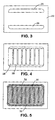
- the resistive element 18 is shown in greater detail in the plan cross-section view of Figure 2. The detailed construction of the resistive element 18 is best explained with reference to the drawings of Figures 3 to 5 which show sequentially the manufacturing steps of the resistive element 18.
- parallel metal strips 26 of silver/palladium or silver/platinum metal alloy are printed on the substrate 20 to provide a pair of parallel conductive metal films for electrical contact to the terminals 14.
- the metal strips 26 are fired onto the surface of the substrate 20 forming metallic film contacts and then a plurality of parallel electrically resistive strips 28 are applied to the substrate sparming the gap between the metal strips 26 and partially overlapping the edges of the metal strips 26 at the respective longitudinal ends of the resistive strips 28 such that each resistive strip 28 provides an electrical connection between the metal strips 26.
- the resistive strips 28 are applied to the substrate 20 by screen printing a resistive ink on the surface of the substrate 20 and metal film contacts 26.
- the resistive ink is printed as a thick film, typically 15 to 20 microns. Once the resistive film has been printed, it is fired.
- the insulating film 30 is applied around the entire perimeter of the resistive element 18 so that it surrounds the resistive element 18 with the film 30 overlying the edges of the resistive element 18 and the surface of the ceramic substrate adjacent thereto.
- the insulating film 30 is applied as a rectangular block covering the resistive strips 28 including the region between the resistive strips 28 as well as the ceramic substrate 20 immediately adjacent to the end resistive strips 28.
- the film is also applied around the edges of the metal strips 26 forming the film contacts on opposite sides of the resistive element.
- Film-free contact regions 32 are provided on the strips 26 for electrical connection of the resistive element 18.
- the film-free contact regions 32 are printed with a solder paste for reflow soldering to the connecting leads 22.
- the insulating film 30 overlaps the strips 26 by 2mm or so around its periphery and by the same amount around the respective edges of the end resistive strips 28 adjacent to the respective edges of the substrate.
- the insulating film 30 may be applied over the whole surface of the substrate 20, except for contact regions 32, such that the film is applied up to the edges of the substrate 20 and, if desired, on the surface of the respective side edges of the substrate 20.
- the resistive element 18 has a different configuration to that shown in Figures 2 to 5.
- the resistive element 18 comprises a resistive film 34 in the form of a serpentine provided on the surface of the substrate 20.
- the resistive film 34 is preferably applied to the surface of the substrate 20 by vacuum deposition.
- the resistive film 34 terminates at metal film contacts 36 positioned at both ends of the resistive film 34.
- the insulating film 38 is applied over the entire area of the resistive film 34 as indicated by the hatched region.
- the insulating film 38 defines a border 41 around the edges of the resistive element 18 between the resistive element 18 and the respective edges of the ceramic substrate 20. Insulating film-free regions 40 are provided on the resistive film 34 to allow electrical connection thereto as described.
- the electrical device of Figure 7 is similar to that of Figure 1, except that the heat generating resistive element 18 is disposed between ceramic substrate 20, bonded to the base plate 24 as before, and a second ceramic substrate tile 42 in the interior of the housing 12.
- the resistive element 18 ofthe embodiment of Figure 7 has a different construction to the resistive element 18 of Figure 1 and is best described with reference to Figure 8.
- Figure 8 is a partial cut away plan view of the device shown in Figure 7, as indicated in the direction of arrow A in Figure 7.
- the resistive element 18 comprises an etched metal foil 44 in the form of a serpentine sandwiched between ceramic substrate tiles 20 and 42.
- the surface of the substrate 20 facing the second ceramic tile 42 is coated over the majority of its area with a high resistance thick film 46, typically a screen printed resistive ink which is fired to provide a film having a thickness of 15 to 20 microns.
- the high resistance thick film 46 is provided on at least the area of the substrate 20 in contact with the metal foil 44, and in the embodiment of Figure 8 is applied as rectangular block on the rectangular substrate 20 such that a resistance film-free border region 48 remains around the edge of the ceramic substrate 20 to reduce potential discharge between the resistive element 18 and the ground plane.
- the width of the border region 48 may be, for example, in the range I to 3mm.
- the high resistance thick film 46 electrically connects the surface of the substrate 20 to the metal foil 44 at the same electrical potential.
- the surface of the substrate 20 in contact with the base plate 24 is provided with a conductive film coating so that this side of the substrate 20 can be electrically connected to the base plate 24, preferably by reflow soldering.
- Contacts 50 (only one of which is shown in the drawing of Figure 8) are provided at the respective ends of the metal foil 44.
- the contacts 50 are integral with the metal foil 44 and provide increased surface area for connecting respective terminals (not shown in Figure 7) by well know resistance welding methods.
- the metal foil 44 is joined to the substrates 20 and 42 by a thermally conductive adhesive applied to a small, preferably central, area of the metal foil 44.
- the edges of the high resistance thick film 46 are coated with an insulating film, for example a silica over-glaze or polymer encapsulant, in a similar way that the edges of the resistive element 18 in the embodiment of Figure 1 are coated.
- the insulating film extends around the whole area of the surface of the substrate coated with the high resistance thick film 46.
- the insulating film is applied as a strip of material having a width of say 2mm overlapping the edges of the high resistance thick film 46 and the adjacent ceramic material around the border region 48. This can best shown in the drawing of Figure 9, which schematically shows the location of the high resistance thick film 46.
- Figure 9 the outline of the ceramic substrate 20 is shown in plan view with the area of the high resistance thick film 46 shown in the central region of the substrate 20.
- the edges of the high resistance thick film 46 are indicated at 52 and the edges of the ceramic substrate at 54.
- the area over which the high resistance thick film 46 is applied is indicated by the diagonal hatched lines 56 which surround the border region 48 of the ceramic substrate 20.
- about one-third of the width of the insulating film overlaps the high resistance thick film 46 along the edges 52, whilst the remaining two-thirds overlaps the surface of the ceramic substrate 20 covering the ceramic material immediately adjacent to the edges 52 but not the full width of the border region between the edges 52 and edges of the substrate 20.
- Figure 10 is a plan view similar to Figure 8 of a slightly different embodiment in which the border region 56 of insulating film is applied closer to the edges of the substrate 20 at the corners of the substrate where the contacts 50 are located.
- the border region 56 in Figure 10 has a slightly skewed shape compared with the rectangular frame of the border region 56 in the embodiment of Figure 9.
- the invention also contemplates embodiments in which the resistive element is provided on a cylindrical (tubular or solid) or arcuate shaped dielectric substrate.
- the resistive element may be provided on more than one surface of the substrate, for example the element may be provided on two adjoining surfaces of a dielectric substrate.
- the electrical device may comprise a plurality of resistive elements each provided on a separate layer of dielectric material in a laminated structure.
Landscapes
- Engineering & Computer Science (AREA)
- Microelectronics & Electronic Packaging (AREA)
- Manufacturing & Machinery (AREA)
- Physics & Mathematics (AREA)
- Electromagnetism (AREA)
- Chemical & Material Sciences (AREA)
- Ceramic Engineering (AREA)
- Details Of Resistors (AREA)
- Non-Adjustable Resistors (AREA)
Abstract
Description
- This invention relates to electrical devices such as power resistors and the like and in particular concerns improvements relating to the electrical insulation of such devices.
- Electrical devices such as power resistors and the like generate significant heat during operation and it is usual to provide such devices with a heat transfer medium for transferring heat from the device to a suitable heat sink such a metal plate or other body of heat conducting material.
- A power resistor is described in US-A-5,355,281 in which a heat generating electrically conductive element is secured to one side of a bonded ceramic-copper laminate plate. The heat-generating element is enclosed within a resistor housing by attachment of the heat conducting plate to an open end of the housing. The laminated plate comprises an intermediate layer of nickel-plated copper sandwiched between first and second alumina (aluminium oxide) ceramic layers. The heat-generating element is secured to the alumina substrate on one side of the plate while the ceramic substrate on the other side of the plate is nickel-plated and is located on the exterior of the assembled device. Internally, the element is electrically connected to a terminal provided on the exterior of the housing. Typically in devices of this type the interior of the housing is filled with a so-called "potting compound" of silicon resin insulating material which is mixed under vacuum conditions to eliminate voids in the insulation so that partial discharge of the high voltage resistor element is minimized during operation.
- The service life of high voltage electrical devices is usually limited by breakdown of the insulation, as measured by partial discharge. Partial discharge increases over time as insulation deteriorates due to the growth of voids in the body of the insulation material due to spark erosion. Spark erosion of the insulation occurs due to variations in the electrical field strength at voids in the body of the insulation material and at the edges of the insulation where divergence of the electrical field is greatest. Although partial discharge can be measured relatively easy, it is extremely difficult to predict or observe where it occurs.
- There is a requirement to improve the quality of the insulation and hence partial discharge characteristics and service life of high voltage electrical devices such as power resistors of the aforementioned type.
- According to an aspect of the invention, there is provided an electrical device comprising an electrically conductive resistive element provided on a ceramic substrate for transferring heat from the element, characterised in that a continuous film of electrically insulating material is applied around the perimeter of the resistive element so that the insulating film surrounds the element with the said film overlying the edge or edges of the element and the dielectric material adjacent thereto.
- The continuous film of insulating material surrounding the resistive element can significantly reduce partial discharge of the device. By overlying the edge or edges of the resistive element and the adjacent dielectric, preferably ceramic material, the film can minimise high voltage divergent fields, particularly at surface discontinuities such as at the corners and edges of the resistive element.
- In preferred embodiments the insulating film comprises a thick film silica over-glaze. The over-glaze may comprise, for example, a low temperature glass encapsulant composition or any similar material suitable for forming an insulating and protective (passivation) layer over thick film circuits, particularly over thick film resistors. The insulating film may comprise a thick film polymer encapsulant composition suitable for encapsulation applications on resistor networks and the like. In other embodiments, thin film dielectric materials, such as quartz or alumina, may be used instead.
- The thickness of the insulating film is typically in the range of 3 to 25 microns, and preferably 5 to 20 microns. In embodiments where the insulating film comprises a thick film silica over-glaze or thick film polymer encapsulant the film thickness is preferably 15 to 20 microns. In embodiments where a thin film quartz or alumina dielectric is used the insulating film typically has a thickness of 5 to 10 microns due to the higher dielectric strength of these materials.
- Preferably, the resistive element is applied to the surface of the dielectric material and comprises at least one electrical contact on the surface of the dielectric material and the film overlies the edge or edges of the contact and the dielectric material immediately adjacent to the edge or edges ofthe contact or contacts. In embodiments where one or more electrical contacts are provided on the surface of the dielectric material, the insulating film overlies the edge or edges of the contact or contacts in addition to the resistive material of the element electrically connected to the contact or contacts of the element. In embodiments where the contact or contacts define part of the perimeter of the resistive element, a continuous film of the insulating material surrounds the element.
- The insulating film may be applied over substantially the whole area of the resistive element with the contact or contacts having a film-free region surrounded by the insulating film so that electrical connection may be made to the film-free region of the contact or contacts.
- In embodiments in which the resistive element comprises a resistive film applied to the surface of the dielectric substrate, the resistive film may comprise a resistive ink printed on the surface of the substrate. In such embodiments, it is desirable to first print the metallic film forming the contact or contacts and then the resistive film partially overlapping the metallic film so that the resistive film forms an electrical connection with the conductive metal film.
- In an embodiment of the invention, the resistive element may comprise a highly resistive film applied to at least part of the surface of the dielectric material and further comprise a metallic foil element provided on and electrically connected to the resistive film, by contact or other means. The foil element has a significantly lower electrical resistance than the resistive film. The resistive film readily enables the surface of the dielectric substrate having the resistive film to be electrically connected at the same electrical potential to the foil element.
- In preferred embodiments the insulating film is applied around the perimeter of the high resistance thick film with the insulating film overlying the edges of the resistive film and the adjacent dielectric material. The width of the insulating film may be in the region of about 2 millimetres with a third of the width of the insulating film covering the resistive film and the other two-thirds covering the ceramic substrate immediately adjacent to the edge or edges of the resistive film.
- The metallic foil element is preferably attached to the resistive film on the ceramic substrate by a heat conductive adhesive.
- In embodiments where the resistive element comprises a metallic foil element, the metallic foil element is preferably sandwiched between two dielectric ceramic substrates each of which may have a resistive film on its surface in contact with the foil element.
- In preferred embodiments the dielectric material comprises alumina (aluminium oxide), and preferably the ceramic substrate comprises a substantially planar ceramic tile. A metal or metal alloy conductive film may be applied to the face of the tile on the opposite side ofthe tile to the resistive element so that the tile may be connected to a metallic heat sink for transferring heat from the resistive element during operation.
- In preferred embodiments the resistive element is enclosed within a casing containing an insulating material such as silicon resin.
- The electrical device may be a power resistor, semi-conductor or diode for example.
- The thermally conductive dielectric material may comprise a ceramic material or mica. The dielectric material may be provided on an electrically conductive substrate, for example a plasma sprayed coating on an aluminium substrate or as a porcellainised steel.
- According to another aspect of the present invention there is provided an electrical device comprising an electrically conductive resistive element provided on a heat transfer medium for transferring heat from the element, the heat transfer medium having a layer or body of electrically conductive material and a layer of thermally conductive dielectric material disposed between the element and the said electrically conductive material, characterised in that a continuous film of electrically insulating material is applied around the perimeter of the resistive element to surround the element with the said film overlying the edge or edges of the element and the dielectric material adjacent thereto.
- The invention contemplates electrical devices at various stages of assembly with the dielectric substrate joined to a layer or body of thermally, and possibly, electrically conductive material such as a metallic heat sink and also devices having a resistive element provided on a dielectric substrate only.
- According to another aspect of the invention, there is provided an electrical device comprising an electrically conductive heat generating resistive element provided on a heat transfer medium for transferring heat from the element, the heat transfer medium comprising a layer or body of electrically conductive material and a layer of thermally conductive dielectric material disposed between the element and the said electrically conductive material, the element being in contact with a resistive film provided on the surface of the dielectric material facing the said element; characterised in that a continuous film of electrically insulating material is applied around the perimeter of the resistive film overlying the edge or edges of the resistive film and the dielectric material adjacent thereto.
- Various embodiments of the invention will now be more particularly described, by way of example only, with reference to the accompanying drawings, in which:
- Figure 1 is a cross-section view of a power resistor according to an embodiment of the present invention;
- Figure 2 is a plan cross-section view along line I-I of Figure 1;
- Figure 3 is a plan view of a ceramic substrate having a conductive film printed thereon;
- Figure 4 is a plan view of the ceramic substrate of Figure 3 having a plurality of thin film resistive strips printed on the substrate;
- Figure 5 is a plan view of the substrate of Figure 4 having a film of insulating material material thereon;
- Figure 6 is a view similar to that of Figure 5 of a ceramic substrate having a different pattern of resistive film, electrical contacts and insulated film on the substrate;
- Figure 7 is a cross-section view of a power resistor according to a second embodiment of the invention;
- Figure 8 is a partial cut away view of the power resistor of Figure 7, as viewed in direction A in the drawing of Figure 7; and
- Figure 9 is a plan view of a ceramic substrate having a high resistance film and insulating film applied thereto.
- Figure 10 is a plan view similar to Figure 8 of a different embodiment of power resistor.
- Referring to Figure 1, an
electrical device 10 comprises a power resistor, that is to say a resistor having a power rating of 1 watt or more. The device includes an injection- mouldedhousing 12 having a pair of electrical terminals 14 (only one of which is shown in the drawing of Figure 1) which extend throughrespective bore openings 16 in thehousing 12. Embodiments are also envisaged where fourterminals 14 are provided. Theterminals 14 are electrically connected to a resistor comprising aresistive element 18 provided on a thermally conductive dielectricceramic substrate 20. In this embodiment theceramic substrate 20 comprises an aluminium oxide substrate. Theterminal 14 is connected to theresistive element 18 by a connectinglead 22 soldered to theresistive element 18 as explained in more detail below. Theceramic substrate 20 is bonded, preferably soldered, to a nickel-platedcopper base plate 24 which constitutes a heat sink of the electrical device. The housing is bonded to thebase plate 24, preferably by a silicon-based adhesive. - The
housing 12 sits on thebase plate 24 so that the interior of thehousing 12 is closed by thebase plate 24. The interior of thehousing 12 is "potted" with a silicon resin insulating material in a manner well known to those skilled in the art. Collectively, theceramic substrate 20 andbase plate 24 define a heat transfer medium for transferring heat generated by theresistive element 18 in use. - The
resistive element 18 is shown in greater detail in the plan cross-section view of Figure 2. The detailed construction of theresistive element 18 is best explained with reference to the drawings of Figures 3 to 5 which show sequentially the manufacturing steps of theresistive element 18. - In Figure 3 parallel metal strips 26 of silver/palladium or silver/platinum metal alloy are printed on the
substrate 20 to provide a pair of parallel conductive metal films for electrical contact to theterminals 14. The metal strips 26 are fired onto the surface of thesubstrate 20 forming metallic film contacts and then a plurality of parallel electricallyresistive strips 28 are applied to the substrate sparming the gap between the metal strips 26 and partially overlapping the edges of the metal strips 26 at the respective longitudinal ends of theresistive strips 28 such that eachresistive strip 28 provides an electrical connection between the metal strips 26. Theresistive strips 28 are applied to thesubstrate 20 by screen printing a resistive ink on the surface of thesubstrate 20 andmetal film contacts 26. The resistive ink is printed as a thick film, typically 15 to 20 microns. Once the resistive film has been printed, it is fired. - An electrically insulating
film 30, for example a thick film silica glaze or polymer encapsulant, is applied to the entire region of theresistive element 18 on thesubstrate 20, as shown by the hatched area in the drawing of Figure 5. The insulatingfilm 30 is applied around the entire perimeter of theresistive element 18 so that it surrounds theresistive element 18 with thefilm 30 overlying the edges of theresistive element 18 and the surface of the ceramic substrate adjacent thereto. As can be seen in Figure 5, the insulatingfilm 30 is applied as a rectangular block covering theresistive strips 28 including the region between theresistive strips 28 as well as theceramic substrate 20 immediately adjacent to the end resistive strips 28. The film is also applied around the edges of the metal strips 26 forming the film contacts on opposite sides of the resistive element. Film-free contact regions 32 are provided on thestrips 26 for electrical connection of theresistive element 18. The film-free contact regions 32 are printed with a solder paste for reflow soldering to the connecting leads 22. The insulatingfilm 30 overlaps thestrips 26 by 2mm or so around its periphery and by the same amount around the respective edges of the endresistive strips 28 adjacent to the respective edges of the substrate. In an alternative embodiment to the one illustrated, the insulatingfilm 30 may be applied over the whole surface of thesubstrate 20, except forcontact regions 32, such that the film is applied up to the edges of thesubstrate 20 and, if desired, on the surface of the respective side edges of thesubstrate 20. - Referring now to Figure 6, in this embodiment the
resistive element 18 has a different configuration to that shown in Figures 2 to 5. In this embodiment theresistive element 18 comprises aresistive film 34 in the form of a serpentine provided on the surface of thesubstrate 20. Theresistive film 34 is preferably applied to the surface of thesubstrate 20 by vacuum deposition. Theresistive film 34 terminates atmetal film contacts 36 positioned at both ends of theresistive film 34. In this arrangement, the insulatingfilm 38 is applied over the entire area of theresistive film 34 as indicated by the hatched region. The insulatingfilm 38 defines aborder 41 around the edges of theresistive element 18 between theresistive element 18 and the respective edges of theceramic substrate 20. Insulating film-free regions 40 are provided on theresistive film 34 to allow electrical connection thereto as described. - The electrical device of Figure 7 is similar to that of Figure 1, except that the heat generating
resistive element 18 is disposed betweenceramic substrate 20, bonded to thebase plate 24 as before, and a secondceramic substrate tile 42 in the interior of thehousing 12. - The
resistive element 18 ofthe embodiment of Figure 7 has a different construction to theresistive element 18 of Figure 1 and is best described with reference to Figure 8. Figure 8 is a partial cut away plan view of the device shown in Figure 7, as indicated in the direction of arrow A in Figure 7. In this embodiment theresistive element 18 comprises an etchedmetal foil 44 in the form of a serpentine sandwiched betweenceramic substrate tiles - The surface of the
substrate 20 facing the secondceramic tile 42 is coated over the majority of its area with a high resistancethick film 46, typically a screen printed resistive ink which is fired to provide a film having a thickness of 15 to 20 microns. The high resistancethick film 46 is provided on at least the area of thesubstrate 20 in contact with themetal foil 44, and in the embodiment of Figure 8 is applied as rectangular block on therectangular substrate 20 such that a resistance film-free border region 48 remains around the edge of theceramic substrate 20 to reduce potential discharge between theresistive element 18 and the ground plane. The width of theborder region 48 may be, for example, in the range I to 3mm. The high resistancethick film 46 electrically connects the surface of thesubstrate 20 to themetal foil 44 at the same electrical potential. - As previously mentioned in relation to the embodiment of Figure 1 the surface of the
substrate 20 in contact with thebase plate 24 is provided with a conductive film coating so that this side of thesubstrate 20 can be electrically connected to thebase plate 24, preferably by reflow soldering. Contacts 50 (only one of which is shown in the drawing of Figure 8) are provided at the respective ends of themetal foil 44. Thecontacts 50 are integral with themetal foil 44 and provide increased surface area for connecting respective terminals (not shown in Figure 7) by well know resistance welding methods. Themetal foil 44 is joined to thesubstrates metal foil 44. - The edges of the high resistance
thick film 46 are coated with an insulating film, for example a silica over-glaze or polymer encapsulant, in a similar way that the edges of theresistive element 18 in the embodiment of Figure 1 are coated. The insulating film extends around the whole area of the surface of the substrate coated with the high resistancethick film 46. The insulating film is applied as a strip of material having a width of say 2mm overlapping the edges of the high resistancethick film 46 and the adjacent ceramic material around theborder region 48. This can best shown in the drawing of Figure 9, which schematically shows the location of the high resistancethick film 46. In Figure 9 the outline of theceramic substrate 20 is shown in plan view with the area of the high resistancethick film 46 shown in the central region of thesubstrate 20. The edges of the high resistancethick film 46 are indicated at 52 and the edges of the ceramic substrate at 54. The area over which the high resistancethick film 46 is applied is indicated by the diagonal hatchedlines 56 which surround theborder region 48 of theceramic substrate 20. As can be seen in Figure 9, about one-third of the width of the insulating film overlaps the high resistancethick film 46 along theedges 52, whilst the remaining two-thirds overlaps the surface of theceramic substrate 20 covering the ceramic material immediately adjacent to theedges 52 but not the full width of the border region between theedges 52 and edges of thesubstrate 20. - Figure 10 is a plan view similar to Figure 8 of a slightly different embodiment in which the
border region 56 of insulating film is applied closer to the edges of thesubstrate 20 at the corners of the substrate where thecontacts 50 are located. Theborder region 56 in Figure 10 has a slightly skewed shape compared with the rectangular frame of theborder region 56 in the embodiment of Figure 9. - Although aspects of the invention have been described with reference to the embodiments shown in the accompanying drawings, it is to be understood that the invention is not limited to those precise embodiments and that various changes and modifications may be effected without further inventive skill and effort. For example, the invention also contemplates embodiments in which the resistive element is provided on a cylindrical (tubular or solid) or arcuate shaped dielectric substrate. In addition the resistive element may be provided on more than one surface of the substrate, for example the element may be provided on two adjoining surfaces of a dielectric substrate. The electrical device may comprise a plurality of resistive elements each provided on a separate layer of dielectric material in a laminated structure.
Claims (22)
- An electrical device comprising an electrically conductive resistive element provided on a thermally conductive dielectric material for transferring heat from the element, characterised in that a continuous film of electrically insulating material is applied around the perimeter of the resistive element so that the insulating film surrounds the element with the said film overlying the edge or edges of the element and the dielectric material adjacent thereto.
- A device as claimed in Claim 1 wherein the insulating film comprises a silica film over glaze, a polymer encapsulant, or a quartz or alumina dielectric.
- A device as claimed in Claim 1 or Claim 2 wherein the thickness of said insulating film is in the range 3 to 25 microns, preferably 5 to 20 microns.
- A device as claimed in any preceding claim wherein the resistive element is applied to the surface of the dielectric material and comprises at least one electrical contact on the said surface and wherein the said film overlies the edge or edges of the said contact and the dielectric material immediately adjacent thereto.
- A device as claimed in Claim 4 wherein the said insulating film is applied over substantially the whole area of the resistive element with the said contact having at least one insulating film free region surrounded by the said film for electrical connection thereto.
- A device as claimed in Claim 4 or Claim 5 wherein the said contact comprises a film of conductive material applied to the surface of the said dielectric material.
- A device as claimed in any of Claims 4 to 6 wherein the resistive element comprises a resistive film applied to the surface of the said dielectric material and the said contact.
- A device as claimed in Claim 6 wherein the resistive film comprises a resistive ink printed on the surface of the said dielectric material.
- A device as claimed in any of Claims 1 to 3 wherein the resistive element comprises a resistive film applied to at least part of the surface of the dielectric material, and a metallic foil element provided on and electrically connected to the said resistive film, the foil element having a lower electrical resistance than the said resistive film.
- A device as claimed in Claim 9 wherein the insulating film is applied around the perimeter of the resistive film overlying the edge or edges of the resistive film and the dielectric material adjacent thereto.
- A device as claimed in Claim 9 or Claim 10 wherein the metallic foil element is attached to the resistive film by a heat conductive adhesive.
- A device as claimed in any of Claims 9 to 11 wherein the metallic foil element is disposed between the said resistive film and a further thermally conductive dielectric material overlying the said resistive film.
- A device as claimed in any preceding claim wherein the dielectric material comprises alumina.
- A device as claimed in any preceding claim wherein the said dielectric material comprises a substantially planar ceramic tile.
- A device as claimed in claim 14 wherein a conductive film is applied to the face of the tile adjacent to the layer or body of electrically conductive material.
- A device as claimed in any preceding claim wherein the said resistive element is enclosed within a casing containing a insulating material.
- An electrical device as claimed in any preceding claim wherein said device comprises a power resistor.
- An electrical device as claimed in any preceding claim wherein the thermally conductive dielectric material is disposed between the resistive element and a second layer or body of thermally conductive material.
- An electrical device as claimed in Claim 18 wherein the second layer or body of thermally conductive material comprises an electrically conductive material.
- An electrical device as claimed in any preceding claim wherein the thermally conductive dielectric material comprises a ceramic material or mica.
- An electrical device comprising an electrically conductive heat generating resistive element provided on a heat transfer medium for transferring heat from the element, the heat transfer medium comprising a layer or body of electrically conductive material and a layer of thermally conductive dielectric material disposed between the element and the said electrically conductive material, the element being in contact with a resistive film provided on the surface of the dielectric material facing the said element; characterised in that a continuous film of electrically insulating material is applied around the perimeter of the resistive film overlying the edge or edges of the resistive film and the dielectric material adjacent thereto.
- An electrical device as herein before described with reference to the accompanying drawings.
Applications Claiming Priority (1)
| Application Number | Priority Date | Filing Date | Title |
|---|---|---|---|
| GBGB0415045.4A GB0415045D0 (en) | 2004-07-05 | 2004-07-05 | Electrical device having a heat generating resistive element |
Publications (2)
| Publication Number | Publication Date |
|---|---|
| EP1615239A1 true EP1615239A1 (en) | 2006-01-11 |
| EP1615239B1 EP1615239B1 (en) | 2014-05-07 |
Family
ID=32843595
Family Applications (1)
| Application Number | Title | Priority Date | Filing Date |
|---|---|---|---|
| EP05253965.7A Expired - Lifetime EP1615239B1 (en) | 2004-07-05 | 2005-06-27 | power resistor having a heat generating resistive element |
Country Status (4)
| Country | Link |
|---|---|
| US (1) | US7427911B2 (en) |
| EP (1) | EP1615239B1 (en) |
| JP (1) | JP4836506B2 (en) |
| GB (1) | GB0415045D0 (en) |
Cited By (1)
| Publication number | Priority date | Publication date | Assignee | Title |
|---|---|---|---|---|
| EP3250003A1 (en) * | 2015-12-18 | 2017-11-29 | E.G.O. ELEKTRO-GERÄTEBAU GmbH | Heating device |
Families Citing this family (4)
| Publication number | Priority date | Publication date | Assignee | Title |
|---|---|---|---|---|
| JP4859144B2 (en) * | 2005-10-03 | 2012-01-25 | アルファ・エレクトロニクス株式会社 | Metal foil resistors |
| US20110292963A1 (en) * | 2010-01-28 | 2011-12-01 | Conductive Compounds, Inc. | Laser position detection system |
| JP5403017B2 (en) * | 2011-08-30 | 2014-01-29 | 株式会社デンソー | Ceramic heater and gas sensor element using the same |
| US20190049077A1 (en) * | 2017-08-11 | 2019-02-14 | Elemental LED, Inc. | Flexible Power Distribution System |
Citations (6)
| Publication number | Priority date | Publication date | Assignee | Title |
|---|---|---|---|---|
| US3654580A (en) * | 1969-03-14 | 1972-04-04 | Sanders Associates Inc | Resistor structure |
| US3813631A (en) * | 1972-08-09 | 1974-05-28 | Hitachi Ltd | High resistance resistor device for dc high voltage circuits |
| DE4300084A1 (en) * | 1993-01-06 | 1994-07-07 | Heraeus Sensor Gmbh | Resistance thermometer used as temp. sensor |
| US5355281A (en) | 1993-06-29 | 1994-10-11 | E.B.G. Elektronische Bauelemente Gesellschaft M.B.H. | Electrical device having a bonded ceramic-copper heat transfer medium |
| EP0713227A1 (en) * | 1994-11-19 | 1996-05-22 | ABB Management AG | Thermistor and current limiting device with at least one thermistor |
| EP0770862A1 (en) * | 1995-05-11 | 1997-05-02 | Matsushita Electric Industrial Co., Ltd. | Temperature sensor element, temperature sensor having the same and method for producing the same temperature sensor element |
Family Cites Families (16)
| Publication number | Priority date | Publication date | Assignee | Title |
|---|---|---|---|---|
| US3955169A (en) * | 1974-11-08 | 1976-05-04 | The United States Of America As Represented By The Secretary Of The Air Force | High power resistor |
| US4677413A (en) * | 1984-11-20 | 1987-06-30 | Vishay Intertechnology, Inc. | Precision power resistor with very low temperature coefficient of resistance |
| US4613844A (en) * | 1985-08-26 | 1986-09-23 | Rca Corporation | High power RF thick film resistor and method for the manufacture thereof |
| US4716396A (en) * | 1986-07-10 | 1987-12-29 | Dale Electronics, Inc. | High power density, low corona resistor |
| JPH01133701U (en) * | 1988-03-07 | 1989-09-12 | ||
| JP2616515B2 (en) * | 1991-06-26 | 1997-06-04 | 日本電気株式会社 | Thick film resistor, thick film printed wiring board, method of manufacturing the same, and thick film hybrid integrated circuit |
| DE69225685T2 (en) | 1991-11-22 | 1998-11-26 | Canon K.K., Tokio/Tokyo | Liquid crystal composition, liquid crystal device and display device |
| JPH07106729A (en) * | 1993-09-30 | 1995-04-21 | Murata Mfg Co Ltd | Thick film circuit component manufacturing method |
| US5481241A (en) * | 1993-11-12 | 1996-01-02 | Caddock Electronics, Inc. | Film-type heat sink-mounted power resistor combination having only a thin encapsulant, and having an enlarged internal heat sink |
| JPH0883701A (en) * | 1994-09-12 | 1996-03-26 | Teikoku Tsushin Kogyo Co Ltd | High power type resistor |
| US5841340A (en) * | 1996-05-07 | 1998-11-24 | Rf Power Components, Inc. | Solderless RF power film resistors and terminations |
| JPH09320805A (en) * | 1996-05-29 | 1997-12-12 | Micron Denki Kk | Automotive AT solenoid valve current limiting resistor and method of manufacturing the same |
| JPH09330801A (en) * | 1996-06-07 | 1997-12-22 | Matsushita Electric Ind Co Ltd | Resistor and manufacturing method thereof |
| US5990780A (en) * | 1998-02-06 | 1999-11-23 | Caddock Electronics, Inc. | Low-resistance, high-power resistor having a tight resistance tolerance despite variations in the circuit connections to the contacts |
| JP2001185407A (en) * | 1999-12-24 | 2001-07-06 | Seiden Techno Co Ltd | POWER RESISTOR, RESISTANCE ELEMENT, AND MANUFACTURING METHOD THEREOF |
| JP4508558B2 (en) * | 2003-06-18 | 2010-07-21 | コーア株式会社 | Electronic component and its manufacturing method |
-
2004
- 2004-07-05 GB GBGB0415045.4A patent/GB0415045D0/en not_active Ceased
-
2005
- 2005-06-27 EP EP05253965.7A patent/EP1615239B1/en not_active Expired - Lifetime
- 2005-07-01 US US11/173,045 patent/US7427911B2/en not_active Expired - Lifetime
- 2005-07-05 JP JP2005195882A patent/JP4836506B2/en not_active Expired - Lifetime
Patent Citations (6)
| Publication number | Priority date | Publication date | Assignee | Title |
|---|---|---|---|---|
| US3654580A (en) * | 1969-03-14 | 1972-04-04 | Sanders Associates Inc | Resistor structure |
| US3813631A (en) * | 1972-08-09 | 1974-05-28 | Hitachi Ltd | High resistance resistor device for dc high voltage circuits |
| DE4300084A1 (en) * | 1993-01-06 | 1994-07-07 | Heraeus Sensor Gmbh | Resistance thermometer used as temp. sensor |
| US5355281A (en) | 1993-06-29 | 1994-10-11 | E.B.G. Elektronische Bauelemente Gesellschaft M.B.H. | Electrical device having a bonded ceramic-copper heat transfer medium |
| EP0713227A1 (en) * | 1994-11-19 | 1996-05-22 | ABB Management AG | Thermistor and current limiting device with at least one thermistor |
| EP0770862A1 (en) * | 1995-05-11 | 1997-05-02 | Matsushita Electric Industrial Co., Ltd. | Temperature sensor element, temperature sensor having the same and method for producing the same temperature sensor element |
Cited By (1)
| Publication number | Priority date | Publication date | Assignee | Title |
|---|---|---|---|---|
| EP3250003A1 (en) * | 2015-12-18 | 2017-11-29 | E.G.O. ELEKTRO-GERÄTEBAU GmbH | Heating device |
Also Published As
| Publication number | Publication date |
|---|---|
| US7427911B2 (en) | 2008-09-23 |
| EP1615239B1 (en) | 2014-05-07 |
| GB0415045D0 (en) | 2004-08-04 |
| US20060108353A1 (en) | 2006-05-25 |
| JP2006024933A (en) | 2006-01-26 |
| JP4836506B2 (en) | 2011-12-14 |
Similar Documents
| Publication | Publication Date | Title |
|---|---|---|
| US7782173B2 (en) | Chip resistor | |
| JP2024010234A (en) | chip resistor | |
| US9754705B2 (en) | Resistor, method of manufacturing the same, and board having the same | |
| CN113206048B (en) | Semiconductor device and method for manufacturing the same | |
| KR100823378B1 (en) | Ceramic heating element | |
| KR100349780B1 (en) | Chip Thermistor | |
| CN100530485C (en) | Chip fuse box | |
| CN107545968B (en) | Resistor element and resistor element mounting board | |
| US7427911B2 (en) | Electrical device having a heat generating resistive element | |
| WO2022091644A1 (en) | Chip resistor | |
| JPH09320802A (en) | Resistor | |
| KR101075664B1 (en) | Chip resister and method of manufacturing the same | |
| CN113826173B (en) | Resistor | |
| US20070096864A1 (en) | Surface mount composite electronic component and method for manufacturing same | |
| JPH10308157A (en) | fuse | |
| JP4295035B2 (en) | Manufacturing method of chip resistor | |
| JP2001160502A (en) | Surge absorbing element and method of manufacturing the same | |
| KR101771818B1 (en) | Resistor element and board having the same mounted thereon | |
| JP2001126901A (en) | Chip components | |
| KR101771836B1 (en) | Chip resistor and chip resistor assembly | |
| JP2004288661A (en) | Wiring board | |
| JP3464138B2 (en) | Electronic component storage package | |
| US20190013120A1 (en) | Component substrate having a protective function and method for production thereof | |
| KR20180017842A (en) | Chip resistor and chip resistor assembly | |
| JP2004179111A (en) | Chip type surge absorber and method of manufacturing the same |
Legal Events
| Date | Code | Title | Description |
|---|---|---|---|
| PUAI | Public reference made under article 153(3) epc to a published international application that has entered the european phase |
Free format text: ORIGINAL CODE: 0009012 |
|
| AK | Designated contracting states |
Kind code of ref document: A1 Designated state(s): AT BE BG CH CY CZ DE DK EE ES FI FR GB GR HU IE IS IT LI LT LU MC NL PL PT RO SE SI SK TR |
|
| AX | Request for extension of the european patent |
Extension state: AL BA HR LV MK YU |
|
| 17P | Request for examination filed |
Effective date: 20060629 |
|
| AKX | Designation fees paid |
Designated state(s): AT BE BG CH CY CZ DE DK EE ES FI FR GB GR HU IE IS IT LI LT LU MC NL PL PT RO SE SI SK TR |
|
| 17Q | First examination report despatched |
Effective date: 20080526 |
|
| GRAP | Despatch of communication of intention to grant a patent |
Free format text: ORIGINAL CODE: EPIDOSNIGR1 |
|
| INTG | Intention to grant announced |
Effective date: 20131122 |
|
| GRAS | Grant fee paid |
Free format text: ORIGINAL CODE: EPIDOSNIGR3 |
|
| GRAA | (expected) grant |
Free format text: ORIGINAL CODE: 0009210 |
|
| AK | Designated contracting states |
Kind code of ref document: B1 Designated state(s): AT BE BG CH CY CZ DE DK EE ES FI FR GB GR HU IE IS IT LI LT LU MC NL PL PT RO SE SI SK TR |
|
| REG | Reference to a national code |
Ref country code: GB Ref legal event code: FG4D |
|
| REG | Reference to a national code |
Ref country code: AT Ref legal event code: REF Ref document number: 667230 Country of ref document: AT Kind code of ref document: T Effective date: 20140515 |
|
| REG | Reference to a national code |
Ref country code: IE Ref legal event code: FG4D |
|
| REG | Reference to a national code |
Ref country code: DE Ref legal event code: R096 Ref document number: 602005043521 Country of ref document: DE Effective date: 20140618 |
|
| REG | Reference to a national code |
Ref country code: NL Ref legal event code: VDEP Effective date: 20140507 |
|
| REG | Reference to a national code |
Ref country code: LT Ref legal event code: MG4D |
|
| PG25 | Lapsed in a contracting state [announced via postgrant information from national office to epo] |
Ref country code: GR Free format text: LAPSE BECAUSE OF FAILURE TO SUBMIT A TRANSLATION OF THE DESCRIPTION OR TO PAY THE FEE WITHIN THE PRESCRIBED TIME-LIMIT Effective date: 20140808 Ref country code: IS Free format text: LAPSE BECAUSE OF FAILURE TO SUBMIT A TRANSLATION OF THE DESCRIPTION OR TO PAY THE FEE WITHIN THE PRESCRIBED TIME-LIMIT Effective date: 20140907 Ref country code: FI Free format text: LAPSE BECAUSE OF FAILURE TO SUBMIT A TRANSLATION OF THE DESCRIPTION OR TO PAY THE FEE WITHIN THE PRESCRIBED TIME-LIMIT Effective date: 20140507 Ref country code: LT Free format text: LAPSE BECAUSE OF FAILURE TO SUBMIT A TRANSLATION OF THE DESCRIPTION OR TO PAY THE FEE WITHIN THE PRESCRIBED TIME-LIMIT Effective date: 20140507 Ref country code: CY Free format text: LAPSE BECAUSE OF FAILURE TO SUBMIT A TRANSLATION OF THE DESCRIPTION OR TO PAY THE FEE WITHIN THE PRESCRIBED TIME-LIMIT Effective date: 20140507 |
|
| PG25 | Lapsed in a contracting state [announced via postgrant information from national office to epo] |
Ref country code: ES Free format text: LAPSE BECAUSE OF FAILURE TO SUBMIT A TRANSLATION OF THE DESCRIPTION OR TO PAY THE FEE WITHIN THE PRESCRIBED TIME-LIMIT Effective date: 20140507 Ref country code: PL Free format text: LAPSE BECAUSE OF FAILURE TO SUBMIT A TRANSLATION OF THE DESCRIPTION OR TO PAY THE FEE WITHIN THE PRESCRIBED TIME-LIMIT Effective date: 20140507 Ref country code: SE Free format text: LAPSE BECAUSE OF FAILURE TO SUBMIT A TRANSLATION OF THE DESCRIPTION OR TO PAY THE FEE WITHIN THE PRESCRIBED TIME-LIMIT Effective date: 20140507 |
|
| PG25 | Lapsed in a contracting state [announced via postgrant information from national office to epo] |
Ref country code: PT Free format text: LAPSE BECAUSE OF FAILURE TO SUBMIT A TRANSLATION OF THE DESCRIPTION OR TO PAY THE FEE WITHIN THE PRESCRIBED TIME-LIMIT Effective date: 20140908 |
|
| PG25 | Lapsed in a contracting state [announced via postgrant information from national office to epo] |
Ref country code: BE Free format text: LAPSE BECAUSE OF FAILURE TO SUBMIT A TRANSLATION OF THE DESCRIPTION OR TO PAY THE FEE WITHIN THE PRESCRIBED TIME-LIMIT Effective date: 20140507 Ref country code: EE Free format text: LAPSE BECAUSE OF FAILURE TO SUBMIT A TRANSLATION OF THE DESCRIPTION OR TO PAY THE FEE WITHIN THE PRESCRIBED TIME-LIMIT Effective date: 20140507 Ref country code: DK Free format text: LAPSE BECAUSE OF FAILURE TO SUBMIT A TRANSLATION OF THE DESCRIPTION OR TO PAY THE FEE WITHIN THE PRESCRIBED TIME-LIMIT Effective date: 20140507 Ref country code: RO Free format text: LAPSE BECAUSE OF FAILURE TO SUBMIT A TRANSLATION OF THE DESCRIPTION OR TO PAY THE FEE WITHIN THE PRESCRIBED TIME-LIMIT Effective date: 20140507 Ref country code: SK Free format text: LAPSE BECAUSE OF FAILURE TO SUBMIT A TRANSLATION OF THE DESCRIPTION OR TO PAY THE FEE WITHIN THE PRESCRIBED TIME-LIMIT Effective date: 20140507 Ref country code: CZ Free format text: LAPSE BECAUSE OF FAILURE TO SUBMIT A TRANSLATION OF THE DESCRIPTION OR TO PAY THE FEE WITHIN THE PRESCRIBED TIME-LIMIT Effective date: 20140507 |
|
| REG | Reference to a national code |
Ref country code: CH Ref legal event code: PL |
|
| REG | Reference to a national code |
Ref country code: DE Ref legal event code: R097 Ref document number: 602005043521 Country of ref document: DE |
|
| PG25 | Lapsed in a contracting state [announced via postgrant information from national office to epo] |
Ref country code: NL Free format text: LAPSE BECAUSE OF FAILURE TO SUBMIT A TRANSLATION OF THE DESCRIPTION OR TO PAY THE FEE WITHIN THE PRESCRIBED TIME-LIMIT Effective date: 20140507 |
|
| PLBE | No opposition filed within time limit |
Free format text: ORIGINAL CODE: 0009261 |
|
| STAA | Information on the status of an ep patent application or granted ep patent |
Free format text: STATUS: NO OPPOSITION FILED WITHIN TIME LIMIT |
|
| REG | Reference to a national code |
Ref country code: IE Ref legal event code: MM4A |
|
| 26N | No opposition filed |
Effective date: 20150210 |
|
| PG25 | Lapsed in a contracting state [announced via postgrant information from national office to epo] |
Ref country code: CH Free format text: LAPSE BECAUSE OF NON-PAYMENT OF DUE FEES Effective date: 20140630 Ref country code: IT Free format text: LAPSE BECAUSE OF FAILURE TO SUBMIT A TRANSLATION OF THE DESCRIPTION OR TO PAY THE FEE WITHIN THE PRESCRIBED TIME-LIMIT Effective date: 20140507 Ref country code: IE Free format text: LAPSE BECAUSE OF NON-PAYMENT OF DUE FEES Effective date: 20140627 Ref country code: LI Free format text: LAPSE BECAUSE OF NON-PAYMENT OF DUE FEES Effective date: 20140630 |
|
| REG | Reference to a national code |
Ref country code: DE Ref legal event code: R097 Ref document number: 602005043521 Country of ref document: DE Effective date: 20150210 |
|
| PG25 | Lapsed in a contracting state [announced via postgrant information from national office to epo] |
Ref country code: SI Free format text: LAPSE BECAUSE OF FAILURE TO SUBMIT A TRANSLATION OF THE DESCRIPTION OR TO PAY THE FEE WITHIN THE PRESCRIBED TIME-LIMIT Effective date: 20140507 |
|
| PG25 | Lapsed in a contracting state [announced via postgrant information from national office to epo] |
Ref country code: MC Free format text: LAPSE BECAUSE OF FAILURE TO SUBMIT A TRANSLATION OF THE DESCRIPTION OR TO PAY THE FEE WITHIN THE PRESCRIBED TIME-LIMIT Effective date: 20140507 |
|
| PG25 | Lapsed in a contracting state [announced via postgrant information from national office to epo] |
Ref country code: BG Free format text: LAPSE BECAUSE OF FAILURE TO SUBMIT A TRANSLATION OF THE DESCRIPTION OR TO PAY THE FEE WITHIN THE PRESCRIBED TIME-LIMIT Effective date: 20140507 |
|
| REG | Reference to a national code |
Ref country code: FR Ref legal event code: PLFP Year of fee payment: 12 |
|
| PG25 | Lapsed in a contracting state [announced via postgrant information from national office to epo] |
Ref country code: TR Free format text: LAPSE BECAUSE OF FAILURE TO SUBMIT A TRANSLATION OF THE DESCRIPTION OR TO PAY THE FEE WITHIN THE PRESCRIBED TIME-LIMIT Effective date: 20140507 Ref country code: LU Free format text: LAPSE BECAUSE OF NON-PAYMENT OF DUE FEES Effective date: 20140627 Ref country code: HU Free format text: LAPSE BECAUSE OF FAILURE TO SUBMIT A TRANSLATION OF THE DESCRIPTION OR TO PAY THE FEE WITHIN THE PRESCRIBED TIME-LIMIT; INVALID AB INITIO Effective date: 20050627 |
|
| REG | Reference to a national code |
Ref country code: FR Ref legal event code: PLFP Year of fee payment: 13 |
|
| REG | Reference to a national code |
Ref country code: FR Ref legal event code: PLFP Year of fee payment: 14 |
|
| PGFP | Annual fee paid to national office [announced via postgrant information from national office to epo] |
Ref country code: GB Payment date: 20240509 Year of fee payment: 20 |
|
| PGFP | Annual fee paid to national office [announced via postgrant information from national office to epo] |
Ref country code: DE Payment date: 20240502 Year of fee payment: 20 |
|
| PGFP | Annual fee paid to national office [announced via postgrant information from national office to epo] |
Ref country code: AT Payment date: 20240529 Year of fee payment: 20 |
|
| PGFP | Annual fee paid to national office [announced via postgrant information from national office to epo] |
Ref country code: FR Payment date: 20240509 Year of fee payment: 20 |
|
| REG | Reference to a national code |
Ref country code: DE Ref legal event code: R071 Ref document number: 602005043521 Country of ref document: DE |
|
| PG25 | Lapsed in a contracting state [announced via postgrant information from national office to epo] |
Ref country code: GB Free format text: LAPSE BECAUSE OF EXPIRATION OF PROTECTION Effective date: 20250626 |
|
| REG | Reference to a national code |
Ref country code: GB Ref legal event code: PE20 Expiry date: 20250626 |