EP1615225B1 - Verfahren zum dauerhaften Schreibschutz für einen Teilbereich einer Speicherkarte und entsprechende Speicherkarte - Google Patents
Verfahren zum dauerhaften Schreibschutz für einen Teilbereich einer Speicherkarte und entsprechende Speicherkarte Download PDFInfo
- Publication number
- EP1615225B1 EP1615225B1 EP04396046A EP04396046A EP1615225B1 EP 1615225 B1 EP1615225 B1 EP 1615225B1 EP 04396046 A EP04396046 A EP 04396046A EP 04396046 A EP04396046 A EP 04396046A EP 1615225 B1 EP1615225 B1 EP 1615225B1
- Authority
- EP
- European Patent Office
- Prior art keywords
- memory
- write
- memory card
- card
- command
- Prior art date
- Legal status (The legal status is an assumption and is not a legal conclusion. Google has not performed a legal analysis and makes no representation as to the accuracy of the status listed.)
- Expired - Lifetime
Links
Images


Classifications
-
- G—PHYSICS
- G06—COMPUTING OR CALCULATING; COUNTING
- G06F—ELECTRIC DIGITAL DATA PROCESSING
- G06F12/00—Accessing, addressing or allocating within memory systems or architectures
- G06F12/14—Protection against unauthorised use of memory or access to memory
- G06F12/1416—Protection against unauthorised use of memory or access to memory by checking the object accessibility, e.g. type of access defined by the memory independently of subject rights
- G06F12/1425—Protection against unauthorised use of memory or access to memory by checking the object accessibility, e.g. type of access defined by the memory independently of subject rights the protection being physical, e.g. cell, word, block
- G06F12/1433—Protection against unauthorised use of memory or access to memory by checking the object accessibility, e.g. type of access defined by the memory independently of subject rights the protection being physical, e.g. cell, word, block for a module or a part of a module
Definitions
- the present invention relates to a method for permanently write protecting a portion of a memory card and partially permanently write protected memory card.
- This invention also relates to an electronic device, a software, a system and a module utilizing the method of the invention.
- Different types of memory cards such as Compact Flash, Secure Digital or multimedia cards (MMC) are used in various small electronic devices such as personal digital assistants (PDA) or mobile terminals to store data.
- PDA personal digital assistants
- This data can be for example a program that is run on the device or data stored by the user.
- a method for permanently write protecting a part of memory of a memory card is defined by claim 1.
- the method comprises steps of defining at least one unused bit in a specific data register of said memory card to indicate that permanent write protection of the part of the memory is allowed, setting said at least one bit in order to redefine the command to allow permanent write protection of the part of the memory of said memory card, and executing the command in order to permanently write protect said at least one part of the memory.
- Still other embodiments of the invention provide an electronic device and a computer programmable product which use the method of the invention.
- the PARTIAL_PERM_WP bit In order to maintain backwards compatibility, the PARTIAL_PERM_WP bit should be re-programmable. Additionally, in order to prevent accidental permanent protection, the PARTIAL_TERM_WP bit could be cleared automatically when SET_WRITE_PROTECT 5 command is received. This requires that the PARTIAL_PERM_WP bit is set individually each time a write protect group is write protected. Part of the CSD 2 (Table 22 of the MMC specification) fields according to the embodiment of invention is presented in Table 2. Table 2 permanent write protection of write protect groups PARTIAL_PERM_WP 1 R/W/E [17:17]
- CMD31 As another example for understanding the invention for partially write protecting a portion of a MMC 1, there is defined a new command 5 (CMD31). This command would permanently protect individual write protection groups. The segments of the card that can be write protected are defined using WP_GRP_SIZE bits of CSD 2 as usual. SET_PERM_WRITE_PROT command then sets the write protection of the addressed write protection group.
- MMC state diagram data transfer mode
- Fig. 3 MMC state diagram (data transfer mode) according to this other example can be seen in Fig. 3 .
- first CMD7 is sent in order to select one card and put it in the Transfer State (tran). After this CMD31 is sent and after successful operation the MMC returns back to Transfer State (tran). All data communication in data transfer mode is point-to point between the host and the selected card.
- This SET_EDIT_PORT command defines a portion that is editable by the user in the memory 4 of the MMC 1. After this command is performed, the commands that edit (writes, removes or alters) the data can only be directed to this portion, and the write protected portion 3 is left intact.
- a new type of memory card according to the invention could also be added to the MMC specification.
- This new type of MMC memory card has for example one permanently write protected area and one user editable area.
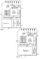
- the partially write protected memory card 1 contains primary technology memory portion 8 and at least one secondary technology memory portion 9. These memory technologies can for example be FLASH and ROM.
- the memory card 1 according to the invention also contains an additional data register 7 (Extended CSD, EXT_CSD), in which the existence and characteristics of the secondary technology memory portion 9 are described.
- EXT_CSD 7 Extended CSD, Extended CSD, EXT_CSD
- the structure of this EXT_CSD 7 is similar to the structure of the CSD 2.
- the primary technology memory portion is active after power up. All register data (for example CSD, access times and density) contained on the MMC applies to this primary technology portion 8. This ensures that the MMC is backwards compatible with the previous versions of the MMC specification.
- the Extended CSD (EXT_CSD) register is read.
- the partially write protected memory card 1 also contains at least two technology memory portions 8 and 9.
- the existence and characteristics of the memory portions 8 and 9 are described in the EXT_CSD register 7.
- both technology memory portions are active after power up, and accessing of both memory portions 8 and 9 is done after reading the Extended CSD register 7.
- the second technology memory portion 9 is Read Only Memory.
- This ROM portion appears as write protected area of the memory of the memory card 1. This size of this area is defined using write protect group size bit in the CSD 2. Also this embodiment is backwards compatible with the previous versions of the MMC specification.
- the device 6 which uses the method of the invention can be for example a mobile terminal or a memory card reader/controller.
- This device 6 will conform physically and electronically with the standards of the memory card in use.
- This standard can for example be the MMC specification.
- the device 6 can comprise a user interface 11, central processor 12 and internal memory 13. These different blocks of the device 6 are connected to each other and to the MMC 1 via data bus. If a software is used to permanently write protect a portion of a memory card 1, the software can be stored in the internal memory 13 of the device 6, and executed in the central processor 12.
Landscapes
- Engineering & Computer Science (AREA)
- Theoretical Computer Science (AREA)
- Computer Security & Cryptography (AREA)
- Physics & Mathematics (AREA)
- General Engineering & Computer Science (AREA)
- General Physics & Mathematics (AREA)
- Storage Device Security (AREA)
Claims (19)
- Verfahren zum permanenten Schreib schützen eines Teils eines Speichers (4) einer Speicherkarte (1), umfassend- Schreibschützen zumindest eines Teils des Speichers (4) durch einen Befehl (5),
dadurch gekennzeichnet, dass es umfasst- Definieren zumindest eines nicht verwendeten Bits in einem bestimmten Speicherregister (2) der Speicherkarte (1), um anzuzeigen, dass permanenter Schreibschutz des Teils des Speichers (4) erlaubt ist,- Setzen des zumindest einen Bits, um den Befehl neu zu definieren, um dauerhaften Schreibschutz des Teils des Speichers (4) der Speicherkarte (1) zu erlauben,- Ausführen des Befehls (5), um den zumindest einen Teil des Speichers (4) permanent schreibzuschützen. - Verfahren gemäß Anspruch 1, wobei das zumindest eine Bit einen gewissen vorbestimmten Wert aufweist.
- Verfahren gemäß Anspruch 1, wobei das zumindest eine Bit reprogrammierbar ist.
- Verfahren gemäß einem der Ansprüche 1 bis 3, wobei das Ausführen des Befehls (5) das zumindest eine Bit automatisch ausziffert.
- Verfahren gemäß einem der Ansprüche 1 bis 4, wobei der zumindest eine Teil des Speichers (4) zumindest eine Speichergruppe umfasst, welche eine gewisse Speichergröße aufweist, die in dem bestimmten Speicherregister definiert ist (2).
- Verfahren gemäß Anspruch 5, wobei das Neudefinieren des Befehls (5) individuell den permantenen Schreibschutz jeder Speichergruppe erlaubt.
- Verfahren gemäß einem der vorhergehenden Ansprüche, wobei die Speicherkarte (1) eine Multimedia-Karte (MMC) ist.
- Teilweise permanent schreibgeschützte Speicherkarte (1), umfassend eine Karten-Schnittstellen-Steuerung (10), der angeordnet ist, um zumindest einen Teil des Speichers (4) durch einen Befehl (5) schreibzuschützen, dadurch gekennzeichnet, dass ein bestimmtes Speicherregister (2) angeordnet ist, um zumindest ein Bit zu definieren, um anzugeben, dass permanenter Schreibschutz des Teils des Speichers (4) erlaubt ist, wobei die Steuerung (10) angeordnet ist, um das zumindest eine Bit zu bestimmen, um den Befehl (5) neu zu definieren, um permanenten Schreibschutz des Teils des Speichers (4) der Speicherkarte (1) zu erlauben, und wobei die Steuerung (10) angeordnet ist, um den Befehl (5) auszuführen, den zumindest einen Teil des Speichers (4) permanent schreibzuschützen.
- Teilweise permanent schreibgeschützte Speicherkarte (1) gemäß Anspruch 8, wobei der Speicher (4) angeordnet ist, um zumindest eine Speichergruppe zu umfassen.
- Teilweise permanent schreibgeschützte Speicherkarte (1) gemäß Anspruch 9, wobei das bestimmte Speicherregister (2) angeordnet ist, um eine Speichergröße von zumindest einer Speichergruppe zu definieren.
- Teilweise permanent schreibgeschützte Speicherkarte (1) gemäß Anspruch 10, wobei die Steuerung (10) angeordnet ist, um den Befehl (5) zu definieren, um individuell permanenten Schreibschutz jeder Speichergruppe zu erlauben.
- Teilweise permanent schreibgeschützte Speicherkarte (1) gemäß einem der Ansprüche 8 bis 11, wobei ein zusätzliches Speicherregister (7) angeordnet ist, um das Vorhandensein und die Eigenschaften des zumindest einen Teils des Speichers (4) zu steuern.
- Teilweise permanent schreibgeschützte Speicherkarte (1) gemäß Anspruch 12, wobei das zusätzliche Speicherregister (7) angeordnet ist, um den Zugang zu dem zumindest einen Teil des Speichers (4) zu definieren.
- Teilweise permanent schreibgeschützte Speicherkarte (1) gemäß einem der Ansprüche 8 bis 13, wobei der Speicher (4) angeordnet ist, um unterschiedliche Speichertechnologien (8, 9) zu implementieren.
- Teilweise permanent schreibgeschützte Speicherkarte (1) gemäß einem der Ansprüche 8 bis 14, wobei sie eine Multimedia-Karte (MMC) ist.
- Elektronische Vorrichtung (6), umfassend eine Benutzerschnittstelle (11), einen zentralen Prozessor (12) und einen internen Speicher (13), wobei die Vorrichtung (6) weiterhin eine Speicherkarte (1) gemäß einem der Ansprüche 8 bis 15 umfasst.
- Vorrichtung (6) gemäß Anspruch 16, wobei die Vorrichtung (6) weiterhin ein Modul (14) zum Schreibschutz der Speicherkarte (1) umfasst.
- Vorrichtung (6) gemäß einem der Ansprüche 1 bis 17, wobei die Vorrichtung (6) eine der folgenden ist: ein Mobilendgerät und ein Speicherkarten-Leser/-Steuerung.
- Computer-programmierbares Produkt, umfassend computer-ausführbare Code -Mittel zum Durchführen einer der Schritte des Verfahrens nach einem der Ansprüche 1 bis 7, wenn das Produkt in dem Prozessor (10, 12) ausgeführt wird.
Priority Applications (4)
| Application Number | Priority Date | Filing Date | Title |
|---|---|---|---|
| DE602004019279T DE602004019279D1 (de) | 2004-07-08 | 2004-07-08 | Verfahren zum dauerhaften Schreibschutz für einen Teilbereich einer Speicherkarte und entsprechende Speicherkarte |
| EP04396046A EP1615225B1 (de) | 2004-07-08 | 2004-07-08 | Verfahren zum dauerhaften Schreibschutz für einen Teilbereich einer Speicherkarte und entsprechende Speicherkarte |
| AT04396046T ATE422081T1 (de) | 2004-07-08 | 2004-07-08 | Verfahren zum dauerhaften schreibschutz für einen teilbereich einer speicherkarte und entsprechende speicherkarte |
| US11/176,669 US7827370B2 (en) | 2004-07-08 | 2005-07-08 | Partial permanent write protection of a memory card and partially permanently write protected memory card |
Applications Claiming Priority (1)
| Application Number | Priority Date | Filing Date | Title |
|---|---|---|---|
| EP04396046A EP1615225B1 (de) | 2004-07-08 | 2004-07-08 | Verfahren zum dauerhaften Schreibschutz für einen Teilbereich einer Speicherkarte und entsprechende Speicherkarte |
Publications (2)
| Publication Number | Publication Date |
|---|---|
| EP1615225A1 EP1615225A1 (de) | 2006-01-11 |
| EP1615225B1 true EP1615225B1 (de) | 2009-01-28 |
Family
ID=34932021
Family Applications (1)
| Application Number | Title | Priority Date | Filing Date |
|---|---|---|---|
| EP04396046A Expired - Lifetime EP1615225B1 (de) | 2004-07-08 | 2004-07-08 | Verfahren zum dauerhaften Schreibschutz für einen Teilbereich einer Speicherkarte und entsprechende Speicherkarte |
Country Status (4)
| Country | Link |
|---|---|
| US (1) | US7827370B2 (de) |
| EP (1) | EP1615225B1 (de) |
| AT (1) | ATE422081T1 (de) |
| DE (1) | DE602004019279D1 (de) |
Families Citing this family (14)
| Publication number | Priority date | Publication date | Assignee | Title |
|---|---|---|---|---|
| JP2009211153A (ja) * | 2008-02-29 | 2009-09-17 | Toshiba Corp | メモリ装置、情報処理装置及び電力制御方法 |
| US20090307140A1 (en) | 2008-06-06 | 2009-12-10 | Upendra Mardikar | Mobile device over-the-air (ota) registration and point-of-sale (pos) payment |
| US8117378B2 (en) * | 2008-10-29 | 2012-02-14 | Microchip Technology Incorporated | Preventing unintended permanent write-protection |
| US8862767B2 (en) | 2011-09-02 | 2014-10-14 | Ebay Inc. | Secure elements broker (SEB) for application communication channel selector optimization |
| US8971144B2 (en) | 2012-01-19 | 2015-03-03 | Quixant Plc | Hardware write-protection |
| EP3080744A1 (de) | 2013-12-10 | 2016-10-19 | Memory Technologies LLC | Speichermodul mit authentifiziertem speicherzugriff |
| WO2015089230A1 (en) | 2013-12-10 | 2015-06-18 | Memory Technologies Llc | Unified memory type aware storage module |
| US9766823B2 (en) | 2013-12-12 | 2017-09-19 | Memory Technologies Llc | Channel optimized storage modules |
| US9977628B2 (en) * | 2014-04-16 | 2018-05-22 | Sandisk Technologies Llc | Storage module and method for configuring the storage module with memory operation parameters |
| US9767045B2 (en) | 2014-08-29 | 2017-09-19 | Memory Technologies Llc | Control for authenticated accesses to a memory device |
| RU170409U1 (ru) * | 2016-12-28 | 2017-04-24 | Валерий Аркадьевич Конявский | Мобильный компьютер с аппаратной защитой данных |
| WO2020211070A1 (en) * | 2019-04-19 | 2020-10-22 | Intel Corporation | Multi-mode protected memory |
| US11184170B2 (en) * | 2019-06-28 | 2021-11-23 | Micron Technology, Inc. | Public key protection techniques |
| US12242758B2 (en) | 2021-11-09 | 2025-03-04 | Samsung Electronics Co., Ltd. | Storage device and an operating method of a storage controller thereof |
Family Cites Families (3)
| Publication number | Priority date | Publication date | Assignee | Title |
|---|---|---|---|---|
| US5345413A (en) * | 1993-04-01 | 1994-09-06 | Microchip Technology Incorporated | Default fuse condition for memory device after final test |
| US5363334A (en) * | 1993-04-10 | 1994-11-08 | Microchip Technology Incorporated | Write protection security for memory device |
| US6279114B1 (en) * | 1998-11-04 | 2001-08-21 | Sandisk Corporation | Voltage negotiation in a single host multiple cards system |
-
2004
- 2004-07-08 EP EP04396046A patent/EP1615225B1/de not_active Expired - Lifetime
- 2004-07-08 DE DE602004019279T patent/DE602004019279D1/de not_active Expired - Lifetime
- 2004-07-08 AT AT04396046T patent/ATE422081T1/de not_active IP Right Cessation
-
2005
- 2005-07-08 US US11/176,669 patent/US7827370B2/en active Active
Also Published As
| Publication number | Publication date |
|---|---|
| ATE422081T1 (de) | 2009-02-15 |
| EP1615225A1 (de) | 2006-01-11 |
| DE602004019279D1 (de) | 2009-03-19 |
| US20060018154A1 (en) | 2006-01-26 |
| US7827370B2 (en) | 2010-11-02 |
Similar Documents
| Publication | Publication Date | Title |
|---|---|---|
| EP1615225B1 (de) | Verfahren zum dauerhaften Schreibschutz für einen Teilbereich einer Speicherkarte und entsprechende Speicherkarte | |
| US20200333874A1 (en) | Card and host apparatus | |
| JP2537199B2 (ja) | Icカ―ド | |
| US8041912B2 (en) | Memory devices with data protection | |
| US9152562B2 (en) | Storage sub-system for a computer comprising write-once memory devices and write-many memory devices and related method | |
| CN100468307C (zh) | 存储卡和搭载在存储卡中的卡用控制器以及存储卡的处理装置 | |
| WO1999026253A1 (en) | Programmable access protection in a flash memory device | |
| JPH113284A (ja) | 情報記憶媒体およびそのセキュリティ方法 | |
| EP1868097B1 (de) | Chip für eine integrierte Schaltung, Datenleseverfahren und Datenschreibverfahren | |
| JPS62190584A (ja) | 携帯可能電子装置 | |
| US7325144B2 (en) | Portable information processor having password code checking function | |
| US7840745B2 (en) | Data accessing system, controller and storage device having the same, and operation method thereof | |
| JPH0765139A (ja) | Icメモリカード | |
| EP1079340A2 (de) | Gegen unberechtigten Zugriff versicherte Chipkarte | |
| US6415371B1 (en) | Storage system, storage device, storage medium controller, access device, method for protecting data, storage medium and computer data signal | |
| CN114911413B (zh) | 电子装置与其操作方法 | |
| EP1692592B1 (de) | Verfahren zur steuerung des zugangs in einem flash-speicher und system zur implementierung eines solchen verfahrens | |
| JP7005934B2 (ja) | 電子情報記憶媒体、icカード、データ送信方法、データ書き込み方法、データ送信プログラム及びデータ書き込みプログラム | |
| US20060294283A1 (en) | Universal Serial Bus Device | |
| CN100380345C (zh) | 内存结构及其所使用的控制器 | |
| JPH089795Y2 (ja) | Icカード | |
| US20070088927A1 (en) | Method of protecting a storage device for a windows operating system | |
| TWI406175B (zh) | 記憶卡以及用於記憶卡之方法 | |
| JP2537198B2 (ja) | 携帯可能電子装置 | |
| JP2008123450A (ja) | 記録媒体及びメモリアクセス可能な電子機器 |
Legal Events
| Date | Code | Title | Description |
|---|---|---|---|
| PUAI | Public reference made under article 153(3) epc to a published international application that has entered the european phase |
Free format text: ORIGINAL CODE: 0009012 |
|
| AK | Designated contracting states |
Kind code of ref document: A1 Designated state(s): AT BE BG CH CY CZ DE DK EE ES FI FR GB GR HU IE IT LI LU MC NL PL PT RO SE SI SK TR |
|
| AX | Request for extension of the european patent |
Extension state: AL HR LT LV MK |
|
| 17P | Request for examination filed |
Effective date: 20060324 |
|
| AKX | Designation fees paid |
Designated state(s): AT BE BG CH CY CZ DE DK EE ES FI FR GB GR HU IE IT LI LU MC NL PL PT RO SE SI SK TR |
|
| 17Q | First examination report despatched |
Effective date: 20060512 |
|
| RIC1 | Information provided on ipc code assigned before grant |
Ipc: G11C 7/24 20060101ALI20070514BHEP Ipc: G06K 19/073 20060101AFI20070514BHEP |
|
| GRAP | Despatch of communication of intention to grant a patent |
Free format text: ORIGINAL CODE: EPIDOSNIGR1 |
|
| GRAS | Grant fee paid |
Free format text: ORIGINAL CODE: EPIDOSNIGR3 |
|
| GRAA | (expected) grant |
Free format text: ORIGINAL CODE: 0009210 |
|
| AK | Designated contracting states |
Kind code of ref document: B1 Designated state(s): AT BE BG CH CY CZ DE DK EE ES FI FR GB GR HU IE IT LI LU MC NL PL PT RO SE SI SK TR |
|
| REG | Reference to a national code |
Ref country code: GB Ref legal event code: FG4D |
|
| REG | Reference to a national code |
Ref country code: CH Ref legal event code: EP |
|
| REG | Reference to a national code |
Ref country code: IE Ref legal event code: FG4D |
|
| REF | Corresponds to: |
Ref document number: 602004019279 Country of ref document: DE Date of ref document: 20090319 Kind code of ref document: P |
|
| NLV1 | Nl: lapsed or annulled due to failure to fulfill the requirements of art. 29p and 29m of the patents act | ||
| PG25 | Lapsed in a contracting state [announced via postgrant information from national office to epo] |
Ref country code: ES Free format text: LAPSE BECAUSE OF FAILURE TO SUBMIT A TRANSLATION OF THE DESCRIPTION OR TO PAY THE FEE WITHIN THE PRESCRIBED TIME-LIMIT Effective date: 20090509 Ref country code: NL Free format text: LAPSE BECAUSE OF FAILURE TO SUBMIT A TRANSLATION OF THE DESCRIPTION OR TO PAY THE FEE WITHIN THE PRESCRIBED TIME-LIMIT Effective date: 20090128 Ref country code: SI Free format text: LAPSE BECAUSE OF FAILURE TO SUBMIT A TRANSLATION OF THE DESCRIPTION OR TO PAY THE FEE WITHIN THE PRESCRIBED TIME-LIMIT Effective date: 20090128 Ref country code: FI Free format text: LAPSE BECAUSE OF FAILURE TO SUBMIT A TRANSLATION OF THE DESCRIPTION OR TO PAY THE FEE WITHIN THE PRESCRIBED TIME-LIMIT Effective date: 20090128 |
|
| PG25 | Lapsed in a contracting state [announced via postgrant information from national office to epo] |
Ref country code: PT Free format text: LAPSE BECAUSE OF FAILURE TO SUBMIT A TRANSLATION OF THE DESCRIPTION OR TO PAY THE FEE WITHIN THE PRESCRIBED TIME-LIMIT Effective date: 20090629 Ref country code: PL Free format text: LAPSE BECAUSE OF FAILURE TO SUBMIT A TRANSLATION OF THE DESCRIPTION OR TO PAY THE FEE WITHIN THE PRESCRIBED TIME-LIMIT Effective date: 20090128 Ref country code: AT Free format text: LAPSE BECAUSE OF FAILURE TO SUBMIT A TRANSLATION OF THE DESCRIPTION OR TO PAY THE FEE WITHIN THE PRESCRIBED TIME-LIMIT Effective date: 20090128 Ref country code: SE Free format text: LAPSE BECAUSE OF FAILURE TO SUBMIT A TRANSLATION OF THE DESCRIPTION OR TO PAY THE FEE WITHIN THE PRESCRIBED TIME-LIMIT Effective date: 20090428 |
|
| PG25 | Lapsed in a contracting state [announced via postgrant information from national office to epo] |
Ref country code: BE Free format text: LAPSE BECAUSE OF FAILURE TO SUBMIT A TRANSLATION OF THE DESCRIPTION OR TO PAY THE FEE WITHIN THE PRESCRIBED TIME-LIMIT Effective date: 20090128 |
|
| PG25 | Lapsed in a contracting state [announced via postgrant information from national office to epo] |
Ref country code: EE Free format text: LAPSE BECAUSE OF FAILURE TO SUBMIT A TRANSLATION OF THE DESCRIPTION OR TO PAY THE FEE WITHIN THE PRESCRIBED TIME-LIMIT Effective date: 20090128 Ref country code: CZ Free format text: LAPSE BECAUSE OF FAILURE TO SUBMIT A TRANSLATION OF THE DESCRIPTION OR TO PAY THE FEE WITHIN THE PRESCRIBED TIME-LIMIT Effective date: 20090128 Ref country code: DK Free format text: LAPSE BECAUSE OF FAILURE TO SUBMIT A TRANSLATION OF THE DESCRIPTION OR TO PAY THE FEE WITHIN THE PRESCRIBED TIME-LIMIT Effective date: 20090128 |
|
| PG25 | Lapsed in a contracting state [announced via postgrant information from national office to epo] |
Ref country code: SK Free format text: LAPSE BECAUSE OF FAILURE TO SUBMIT A TRANSLATION OF THE DESCRIPTION OR TO PAY THE FEE WITHIN THE PRESCRIBED TIME-LIMIT Effective date: 20090128 Ref country code: RO Free format text: LAPSE BECAUSE OF FAILURE TO SUBMIT A TRANSLATION OF THE DESCRIPTION OR TO PAY THE FEE WITHIN THE PRESCRIBED TIME-LIMIT Effective date: 20090128 |
|
| PLBE | No opposition filed within time limit |
Free format text: ORIGINAL CODE: 0009261 |
|
| STAA | Information on the status of an ep patent application or granted ep patent |
Free format text: STATUS: NO OPPOSITION FILED WITHIN TIME LIMIT |
|
| 26N | No opposition filed |
Effective date: 20091029 |
|
| PG25 | Lapsed in a contracting state [announced via postgrant information from national office to epo] |
Ref country code: BG Free format text: LAPSE BECAUSE OF FAILURE TO SUBMIT A TRANSLATION OF THE DESCRIPTION OR TO PAY THE FEE WITHIN THE PRESCRIBED TIME-LIMIT Effective date: 20090428 |
|
| PG25 | Lapsed in a contracting state [announced via postgrant information from national office to epo] |
Ref country code: MC Free format text: LAPSE BECAUSE OF NON-PAYMENT OF DUE FEES Effective date: 20090731 |
|
| REG | Reference to a national code |
Ref country code: CH Ref legal event code: PL |
|
| REG | Reference to a national code |
Ref country code: IE Ref legal event code: MM4A |
|
| PG25 | Lapsed in a contracting state [announced via postgrant information from national office to epo] |
Ref country code: LI Free format text: LAPSE BECAUSE OF NON-PAYMENT OF DUE FEES Effective date: 20090731 Ref country code: CH Free format text: LAPSE BECAUSE OF NON-PAYMENT OF DUE FEES Effective date: 20090731 |
|
| PG25 | Lapsed in a contracting state [announced via postgrant information from national office to epo] |
Ref country code: IE Free format text: LAPSE BECAUSE OF NON-PAYMENT OF DUE FEES Effective date: 20090708 |
|
| PG25 | Lapsed in a contracting state [announced via postgrant information from national office to epo] |
Ref country code: GR Free format text: LAPSE BECAUSE OF FAILURE TO SUBMIT A TRANSLATION OF THE DESCRIPTION OR TO PAY THE FEE WITHIN THE PRESCRIBED TIME-LIMIT Effective date: 20090429 |
|
| PG25 | Lapsed in a contracting state [announced via postgrant information from national office to epo] |
Ref country code: IT Free format text: LAPSE BECAUSE OF FAILURE TO SUBMIT A TRANSLATION OF THE DESCRIPTION OR TO PAY THE FEE WITHIN THE PRESCRIBED TIME-LIMIT Effective date: 20090128 |
|
| PG25 | Lapsed in a contracting state [announced via postgrant information from national office to epo] |
Ref country code: LU Free format text: LAPSE BECAUSE OF NON-PAYMENT OF DUE FEES Effective date: 20090708 |
|
| PG25 | Lapsed in a contracting state [announced via postgrant information from national office to epo] |
Ref country code: HU Free format text: LAPSE BECAUSE OF FAILURE TO SUBMIT A TRANSLATION OF THE DESCRIPTION OR TO PAY THE FEE WITHIN THE PRESCRIBED TIME-LIMIT Effective date: 20090729 |
|
| PG25 | Lapsed in a contracting state [announced via postgrant information from national office to epo] |
Ref country code: TR Free format text: LAPSE BECAUSE OF FAILURE TO SUBMIT A TRANSLATION OF THE DESCRIPTION OR TO PAY THE FEE WITHIN THE PRESCRIBED TIME-LIMIT Effective date: 20090128 |
|
| PG25 | Lapsed in a contracting state [announced via postgrant information from national office to epo] |
Ref country code: CY Free format text: LAPSE BECAUSE OF FAILURE TO SUBMIT A TRANSLATION OF THE DESCRIPTION OR TO PAY THE FEE WITHIN THE PRESCRIBED TIME-LIMIT Effective date: 20090128 |
|
| REG | Reference to a national code |
Ref country code: GB Ref legal event code: 732E Free format text: REGISTERED BETWEEN 20130815 AND 20130821 |
|
| REG | Reference to a national code |
Ref country code: DE Ref legal event code: R081 Ref document number: 602004019279 Country of ref document: DE Owner name: MEMORY TECHNOLOGIES LLC, US Free format text: FORMER OWNER: NOKIA CORP., ESPOO, FI Effective date: 20131118 Ref country code: DE Ref legal event code: R081 Ref document number: 602004019279 Country of ref document: DE Owner name: MEMORY TECHNOLOGIES LLC, LAS VEGAS, US Free format text: FORMER OWNER: NOKIA CORP., ESPOO, FI Effective date: 20131118 Ref country code: DE Ref legal event code: R081 Ref document number: 602004019279 Country of ref document: DE Owner name: MEMORY TECHNOLOGIES LLC, LAS VEGAS, US Free format text: FORMER OWNER: NOKIA CORP., 02610 ESPOO, FI Effective date: 20131118 |
|
| REG | Reference to a national code |
Ref country code: FR Ref legal event code: TP Owner name: MEMORY TECHNOLOGIES LLC, US Effective date: 20141112 |
|
| REG | Reference to a national code |
Ref country code: FR Ref legal event code: PLFP Year of fee payment: 13 |
|
| REG | Reference to a national code |
Ref country code: FR Ref legal event code: PLFP Year of fee payment: 14 |
|
| REG | Reference to a national code |
Ref country code: FR Ref legal event code: PLFP Year of fee payment: 15 |
|
| P01 | Opt-out of the competence of the unified patent court (upc) registered |
Effective date: 20230512 |
|
| PGFP | Annual fee paid to national office [announced via postgrant information from national office to epo] |
Ref country code: GB Payment date: 20230719 Year of fee payment: 20 |
|
| PGFP | Annual fee paid to national office [announced via postgrant information from national office to epo] |
Ref country code: FR Payment date: 20230725 Year of fee payment: 20 Ref country code: DE Payment date: 20230719 Year of fee payment: 20 |
|
| REG | Reference to a national code |
Ref country code: GB Ref legal event code: PE20 Expiry date: 20240707 |
|
| PG25 | Lapsed in a contracting state [announced via postgrant information from national office to epo] |
Ref country code: GB Free format text: LAPSE BECAUSE OF EXPIRATION OF PROTECTION Effective date: 20240707 |
|
| PG25 | Lapsed in a contracting state [announced via postgrant information from national office to epo] |
Ref country code: GB Free format text: LAPSE BECAUSE OF EXPIRATION OF PROTECTION Effective date: 20240707 |