EP1610461A2 - Digitales adaptives Hysteresesystem - Google Patents
Digitales adaptives Hysteresesystem Download PDFInfo
- Publication number
- EP1610461A2 EP1610461A2 EP05011656A EP05011656A EP1610461A2 EP 1610461 A2 EP1610461 A2 EP 1610461A2 EP 05011656 A EP05011656 A EP 05011656A EP 05011656 A EP05011656 A EP 05011656A EP 1610461 A2 EP1610461 A2 EP 1610461A2
- Authority
- EP
- European Patent Office
- Prior art keywords
- value
- input signal
- output
- digital input
- state
- Prior art date
- Legal status (The legal status is an assumption and is not a legal conclusion. Google has not performed a legal analysis and makes no representation as to the accuracy of the status listed.)
- Withdrawn
Links
- 230000003044 adaptive effect Effects 0.000 title abstract description 3
- 238000000034 method Methods 0.000 claims abstract description 45
- 238000013139 quantization Methods 0.000 abstract description 8
- 238000005070 sampling Methods 0.000 description 10
- 238000010586 diagram Methods 0.000 description 9
- 238000006243 chemical reaction Methods 0.000 description 5
- 230000005236 sound signal Effects 0.000 description 4
- 238000005259 measurement Methods 0.000 description 2
- 239000000654 additive Substances 0.000 description 1
- 230000000996 additive effect Effects 0.000 description 1
- 230000002939 deleterious effect Effects 0.000 description 1
- 230000000694 effects Effects 0.000 description 1
- 230000002708 enhancing effect Effects 0.000 description 1
- 238000012986 modification Methods 0.000 description 1
- 230000004048 modification Effects 0.000 description 1
- 238000012552 review Methods 0.000 description 1
- 238000012546 transfer Methods 0.000 description 1
- 230000001960 triggered effect Effects 0.000 description 1
Images


Classifications
-
- H—ELECTRICITY
- H03—ELECTRONIC CIRCUITRY
- H03H—IMPEDANCE NETWORKS, e.g. RESONANT CIRCUITS; RESONATORS
- H03H17/00—Networks using digital techniques
- H03H17/02—Frequency selective networks
- H03H17/0219—Compensation of undesirable effects, e.g. quantisation noise, overflow
Definitions
- the invention generally relates to analog to digital conversion circuitry and more particularly to hysteresis techniques used in digital measurement systems.
- CDs compact disks
- DAT digital audio tapes
- MP3s digital audio media
- One problem with each of these media is that they use different sampling rates and thus different frequencies when providing audio data. It would be very expensive to build complete subsystems to handle each of the varying rates, so it has been common to use a device called a sample rate converter to transfer audio data from one digital sampling frequency rate to another. For example, a CD is sampled at 44.1 kHz while a DAT is sampled at 48 kHz. The backend of the system is to operate at only a single frequency, thus it is required to convert one of the signals to that desired frequency.
- the DAT frequency sample rate of 48 kHz could be converted to a 44.1 kHz rate, which would then be utilized by a digital/analog converter system to provide the desired analog audio signal. Therefore, only a single set of backend circuitry would be required if the rates were converted to a common rate.
- sample rate converter integrated circuits have been developed which have the capability of converting between various input and output frequencies.
- An example of one of these is the Cirrus Logic CS8420.
- the basic operation of a sample rate converter is that the data is interpolated at an oversampling rate, then resampled at the desired output rate, and then decimated or filtered to produce the final resultant output.
- One of the requirements of this process is that the ratio between the input and output clocks be positively determined. For example, in the CS8420 there are 3 to 1 and I to 3 maximum ratios. Given this relatively limited ratio, the rate measurement circuitry was relatively simple to build.
- an adaptive digital hysteresis technique In an adaptive digital hysteresis technique according to the present invention, two modes are used to develop the output value, rather than the conventional single rounding technique, to reduce the quantization errors.
- floor and ceiling modes To determine which of two different schemes, referred to as floor and ceiling modes, to use, it is necessary to have appropriate trip points to select modes.
- the floor and ceiling trip points are developed based on the value of the input signal. For example, if the input signal exceeds a given amount, floor mode is used, while if it is below a given amount ceiling mode is used. If in a given mode, further data values are received that do not meet or exceed the other trip point, operation continues in the existing mode.
- the output values of the technique have a lower output error as compared to prior art rounding with hysteresis techniques.
- This improved hysteresis technique results in a lower error frequency ratio value in a sample rate converter so that large ratios can be used.
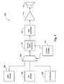
- Figure 1 is a block diagram of an exemplary system having multiple digital audio inputs, each of which has a different sampling rate, which is provided to a single rate conversion and output system.
- Figure 2 is a block diagram of a sample rate converter of Fig. 1.
- Figure 3 is a block diagram of the sample rate converter chip of Fig. 2.
- Figure 4 is a block diagram of the rate estimator block of Fig. 3.
- Figure 5 is a block diagram of the U/8 generator block of Fig. 4.
- Figure 1 illustrates a simplified version of an exemplary audio system, which is capable of receiving signals from three digital audio sources and providing an audio output.
- a first source is a Compact Disk (CD) source 102.
- a second source is a Digital Audio Tape (DAT) 104.
- the third illustrated source is an MP3 source 106.
- the CD source 102 will have the conventional CD sampling rate of 44.1 kHz, while the DAT source will have its conventional sampling rate of 48 kHz.
- An MP3 source may have many different sampling rates, but, in this example, an exemplary rate of 192 kHz is used.
- the outputs from each of these sources 102, 104 and 106 are provided as inputs to a multiplexer 108.
- the multiplexer 108 selects which of the sources are going to be provided to a sample rate converter 110.
- the sample rate converter 110 is used to convert the incoming digital audio signal at its rate into a digital audio signal at a different sampling rate. As an example, assume an output sample rate of 24 kHz from the sample rate converter 110. This output is a very low fidelity output given that the effective upper limit would be approximately 12 kHz but is one, which could be used in many environments as compared to the conventional upper limit of 20 kHz. These environments may include an automobile environment or a simple headset.
- the output of the sample rate converter 110 is provided to a digital to analog (D/A) converter 112.
- D/A digital to analog
- the output of the D/A converter 112 is provided to an amplifier 114, which, in turn, provides an output to a speaker 116 that outputs an audio signal.
- Control circuitry 118 is used to select the input of the multiplexer 108 and to provide the sample rate converter 110 with the desired input frequency and other particular setup parameters.
- the above system is just one simple example for the purpose of illustrating embodiments according to the present invention. Variations are possible, such as different types or numbers of sources and different types of input or output.
- the input and output are simple external connections for the source rate converter, with control settings to program the sample rate converter.
- One such example is used in professional audio equipment.
- FIG. 2 provides a more detailed block diagram of the sample rate converter 110.
- a serial audio input block 200 receives three signals. The SDIN or serial audio data input signal, the ISCLK or input serial audio bit clock signal and the ILRCK or input serial audio left/right clock signal.
- the ILRCK signal is also provided to a phased locked loop (PLL) 202.
- the PLL 202 generates a series of oversampled or multiplied versions of the ILRCK signal for use by a sample rate converter chip 204.
- the sample rate converter chip 204 receives the digital input signal from the serial audio input 200.
- the sample rate converter chip 204 provides its output signal to a serial audio output block 206.
- the output block 206 includes output signals of SDOUT, OSCLK and OLRCK.
- the signals mean serial audio data output signal, output serial audio bit clock signal and output serial audio left/right clock signal.
- the left/right clock signals are the sampling rates for the respective input or output audio data.
- FIG. 3 provides a more detailed block diagram of the sample rate converter chip 204.
- Data is provided at the frequency of the ILRCK signal to an interpolation block 208.
- the interpolation block 208 provides an up-sampled output at a frequency multiple of the ILRCK signal. This output is provided to a resampler block 210.
- the resampler block 210 develops an analog signal from the signal provided by the interpolation block 208 and then samples this analog signal at a multiple of the desired output frequency.
- This digital output at the higher sampling rate is provided to a decimation block 212, which reduces the frequency of the data to the desired frequency.
- a rate estimator block 214 receives the various multiples of the IRLCK and OLRCK signals from the PLL 202 and provides signals to the interpolation block 208 and the resampler 210 block to allow the interpolation block 208 and resampler block 210 to properly up-sample the signal and resample the signal.
- FIG. 4 is a block diagram of the rate estimator block 214.
- a series of multiples of the ILRCK signal preferably 16, 32, 64 and 128 times the input frequency, are provided to rate estimator logic 300.
- signals that are preferably the frequency of the OLRCK signals and 16 times and 128 times the OLRCK frequency are also provided to rate estimator logic 300.
- the ratio generator 302 has an output signal to the rate estimator logic 300 which is a digital value representative of 16 times the ratio between the input frequency and output frequency signals.
- the rate estimator logic 300 uses this output signal from ratio generator 302 in combination with the other signals to provide properly timed signals to the interpolation block 208 and the resampler 210.
- FIG. 5 illustrates a detailed block diagram of the U/8 generator 302.
- the 16 times output frequency (16*f) or OLRCK signal is provided to a 13 bit counter 400.
- the 16 times input frequency (16*f) or ILRCK signal is provided to a 9-bit counter 402.
- the output of the 13-bit counter 400 is in two portions, an upper 8-bit portion and a lower 5-bit portion.
- the upper 8-bit portion and the lower 5-bit portion are provided to a hysteresis rule block 404, which operates according to the hysteresis technique described below.
- the output of the hysteresis rule block 404 is provided to a D flip-flop 406 which is clocked or triggered every time the counter 402 rolls over.
- the rollover signal is also provided to an 8-bit register 408 to latch an 8-bit value into this register 408.
- the upper 8-bits of the 13-bit counter 400 are provided to a floor input of a two (2) input multiplexer 410.
- the 8-bit value is also provided to a one adder so that the 8-bit value plus 1 is provided as the second or ceiling (ceil) input of the multiplexer 410.
- the 8-bit value from the counter 400 or the 8-bit value plus one are the two potential outputs of the multiplexer 410.
- the selection of the particular input is based on the output of the D flip-flop 406, which indicates the hysteresis rule that is in effect.
- the output of the multiplexer 410 is provided to the input of the 8-bit register 408 so that each time the counter 402 rolls over, the upper 8-bits of the counter 400, or potentially one more based on the hysteresis rule, is loaded into the register 408.
- This value in the register 408 is used by the rate estimator logic 300 as the ratio of the input and output sample rates.
- the maximum output error with this scheme is (1.5 - delta). For example, if O[n] is 3, then the maximum M[n] is 4.4999.
- Hysteresis techniques according to the present invention have two modes of operation:
- the floor function rounds positive numbers with a fractional value to the truncated integer and the ceil function rounds positive numbers with a fractional value to the next higher integer. It is understood that the rounding can occur at other than integer values of significance if desired.
- the maximum output error with this scheme is (1 - delta).
- delta is set to the unit in last place or ulp of M[n].
- the hysteresis range remains the same as M[n] changes values. In both schemes, the output is changed to a new value just by hitting the threshold, but it requires another change in M[n] equal to or greater than 1 to pass through the hysteresis region.
- delta is 2 -5 or 0.03125 based on the 5-bit fractional value of the 13-bit counter 400. If one assumes that U/8 must be greater than two for other reasons, then the lowest ceiling trip point is 2.96875 and the lowest floor trip point is 2.03125. Because of uncertainty in the last bit, the actual point may be 2.0625 so that the maximum down sample ratio is 16/2.0625 or 7.76, though the up sample ratio may be 8.
- circuit of Figure 5 could be modified to accomplish this "smaller" case by removing the adder from the ceiling input of the multiplexer 410 and including a subtractor in the floor input.
- the hysteresis technique according to the present invention for the "larger" case is as follows.
- the maximum output error with this scheme is also (2 - delta), with a hysteresis range of +/-1.
- circuit of Figure 5 could be modified to accomplish this "larger" case by having the ceiling input adder add two instead of one and by including an adder in the floor input.
- a hysteresis technique which improves the output of the sample rate converter by reducing errors in the measured input and output frequency ratio value due to quantization errors
Landscapes
- Physics & Mathematics (AREA)
- Engineering & Computer Science (AREA)
- Computer Hardware Design (AREA)
- Mathematical Physics (AREA)
- Analogue/Digital Conversion (AREA)
Applications Claiming Priority (2)
| Application Number | Priority Date | Filing Date | Title |
|---|---|---|---|
| US10/876,030 US20050286380A1 (en) | 2004-06-24 | 2004-06-24 | Digital adaptive hysteresis system |
| US876030 | 2004-06-24 |
Publications (1)
| Publication Number | Publication Date |
|---|---|
| EP1610461A2 true EP1610461A2 (de) | 2005-12-28 |
Family
ID=35033396
Family Applications (1)
| Application Number | Title | Priority Date | Filing Date |
|---|---|---|---|
| EP05011656A Withdrawn EP1610461A2 (de) | 2004-06-24 | 2005-05-31 | Digitales adaptives Hysteresesystem |
Country Status (3)
| Country | Link |
|---|---|
| US (1) | US20050286380A1 (de) |
| EP (1) | EP1610461A2 (de) |
| JP (1) | JP2006050575A (de) |
Family Cites Families (5)
| Publication number | Priority date | Publication date | Assignee | Title |
|---|---|---|---|---|
| JPS63292813A (ja) * | 1987-05-26 | 1988-11-30 | Toshiba Corp | 多入力ディジタルフィルタ |
| JP3199371B2 (ja) * | 1990-07-30 | 2001-08-20 | 松下電器産業株式会社 | 丸め装置 |
| US5654645A (en) * | 1995-07-27 | 1997-08-05 | Cypress Semiconductor Corp. | Buffer with controlled hysteresis |
| US5870320A (en) * | 1997-06-23 | 1999-02-09 | Sun Microsystems, Inc. | Method for reducing a computational result to the range boundaries of a signed 16-bit integer in case of overflow |
| US6529930B1 (en) * | 1998-11-16 | 2003-03-04 | Hitachi America, Ltd. | Methods and apparatus for performing a signed saturation operation |
-
2004
- 2004-06-24 US US10/876,030 patent/US20050286380A1/en not_active Abandoned
-
2005
- 2005-05-31 EP EP05011656A patent/EP1610461A2/de not_active Withdrawn
- 2005-06-23 JP JP2005183681A patent/JP2006050575A/ja active Pending
Also Published As
| Publication number | Publication date |
|---|---|
| US20050286380A1 (en) | 2005-12-29 |
| JP2006050575A (ja) | 2006-02-16 |
Similar Documents
| Publication | Publication Date | Title |
|---|---|---|
| CA1241381A (en) | Interpolating filter arrangement with irrational ratio between the input and the output sampling frequencies | |
| US6215423B1 (en) | Method and system for asynchronous sample rate conversion using a noise-shaped numerically control oscillator | |
| JP3193769B2 (ja) | サンプリング周波数変換器 | |
| US10348326B2 (en) | Digital silicon microphone with interpolation | |
| US20080256157A1 (en) | Information Processing Device and Information Processing Method | |
| US7479912B1 (en) | Low-power high-performance audio DAC system including internal oscillator, FIFO memory, and ASRC | |
| US5880973A (en) | Signal processing system and method for enhanced cascaded integrator-comb interpolation filter stabilization | |
| US7408485B1 (en) | Asynchronous sampling rate converter and method for audio DAC | |
| US6538592B1 (en) | Variable dynamic range analog-to-digital converter | |
| JPH05110442A (ja) | 高次シグマ−デルタ変調器の安定化方法および構成 | |
| US6249235B1 (en) | Sampling frequency conversion apparatus and fractional frequency dividing apparatus for sampling frequency | |
| CN101326725A (zh) | 异步采样率转换器 | |
| TWI232639B (en) | Sigma-delta data conversion employing quantization error feedback | |
| US10659074B2 (en) | Delta-sigma modulator, electronic device, and method for controlling delta-sigma modulator | |
| EP1374415A2 (de) | Delta-sigma-wandler welcher einen multiplizierer enthält | |
| US20060179095A1 (en) | Sample rate converter | |
| US6842131B1 (en) | Delta-sigma modulator | |
| JP2004521568A (ja) | オーバーサンプリングされたデータを用いた端数間引きフィルタ | |
| JP2002076898A (ja) | ノイズシェーパ | |
| KR20060014028A (ko) | 비트 이진 레이트 승산기로 구성된 바이-쿼드 디지털 필터 | |
| KR102895678B1 (ko) | 디지털 마이크로폰들에서의 효율적인 디지털 이득 구현 | |
| EP1610461A2 (de) | Digitales adaptives Hysteresesystem | |
| TW408531B (en) | Signal processing method and device | |
| US6278392B1 (en) | Gain adjustable sigma delta modulator system | |
| JP3510142B2 (ja) | デジタル利得スケーラ/加算器に対するスケーラブルオーバフロークランプおよびこのための方法 |
Legal Events
| Date | Code | Title | Description |
|---|---|---|---|
| PUAI | Public reference made under article 153(3) epc to a published international application that has entered the european phase |
Free format text: ORIGINAL CODE: 0009012 |
|
| 17P | Request for examination filed |
Effective date: 20050630 |
|
| AK | Designated contracting states |
Kind code of ref document: A2 Designated state(s): AT BE BG CH CY CZ DE DK EE ES FI FR GB GR HU IE IS IT LI LT LU MC NL PL PT RO SE SI SK TR |
|
| AX | Request for extension of the european patent |
Extension state: AL BA HR LV MK YU |
|
| RIN1 | Information on inventor provided before grant (corrected) |
Inventor name: KANG, CHANG YONG |
|
| STAA | Information on the status of an ep patent application or granted ep patent |
Free format text: STATUS: THE APPLICATION HAS BEEN WITHDRAWN |
|
| 18W | Application withdrawn |
Effective date: 20080110 |