EP1607899A1 - Kartenerkennung - Google Patents
Kartenerkennung Download PDFInfo
- Publication number
- EP1607899A1 EP1607899A1 EP04253573A EP04253573A EP1607899A1 EP 1607899 A1 EP1607899 A1 EP 1607899A1 EP 04253573 A EP04253573 A EP 04253573A EP 04253573 A EP04253573 A EP 04253573A EP 1607899 A1 EP1607899 A1 EP 1607899A1
- Authority
- EP
- European Patent Office
- Prior art keywords
- signal
- card
- state
- integrated circuit
- semiconductor integrated
- Prior art date
- Legal status (The legal status is an assumption and is not a legal conclusion. Google has not performed a legal analysis and makes no representation as to the accuracy of the status listed.)
- Granted
Links
Images

Classifications
-
- G—PHYSICS
- G06—COMPUTING OR CALCULATING; COUNTING
- G06K—GRAPHICAL DATA READING; PRESENTATION OF DATA; RECORD CARRIERS; HANDLING RECORD CARRIERS
- G06K7/00—Methods or arrangements for sensing record carriers, e.g. for reading patterns
- G06K7/0013—Methods or arrangements for sensing record carriers, e.g. for reading patterns by galvanic contacts, e.g. card connectors for ISO-7816 compliant smart cards or memory cards, e.g. SD card readers
- G06K7/0056—Methods or arrangements for sensing record carriers, e.g. for reading patterns by galvanic contacts, e.g. card connectors for ISO-7816 compliant smart cards or memory cards, e.g. SD card readers housing of the card connector
- G06K7/0069—Methods or arrangements for sensing record carriers, e.g. for reading patterns by galvanic contacts, e.g. card connectors for ISO-7816 compliant smart cards or memory cards, e.g. SD card readers housing of the card connector including means for detecting correct insertion of the card, e.g. end detection switches notifying that the card has been inserted completely and correctly
-
- G—PHYSICS
- G06—COMPUTING OR CALCULATING; COUNTING
- G06K—GRAPHICAL DATA READING; PRESENTATION OF DATA; RECORD CARRIERS; HANDLING RECORD CARRIERS
- G06K7/00—Methods or arrangements for sensing record carriers, e.g. for reading patterns
- G06K7/0013—Methods or arrangements for sensing record carriers, e.g. for reading patterns by galvanic contacts, e.g. card connectors for ISO-7816 compliant smart cards or memory cards, e.g. SD card readers
- G06K7/0021—Methods or arrangements for sensing record carriers, e.g. for reading patterns by galvanic contacts, e.g. card connectors for ISO-7816 compliant smart cards or memory cards, e.g. SD card readers for reading/sensing record carriers having surface contacts
Definitions
- This invention relates to systems utilising cards for storing data, particularly including set-top-boxes for use in pay-television systems.
- a smartcard is a card with an embedded microchip that can be loaded with data. Smartcards are often used in the field of pay-television where a card may be loaded with data including the viewing rights of the card holder. The card may then be inserted into a set-top-box to allow access to particular services. Smartcards also have extensive use in many other applications.
- the detection of an inserted smartcard is used to trigger particular system processes. For example, for security reasons, insertion of a smartcard into a set-top-box may cause a system reset prior to reading data from the card. Detection of a smartcard is often performed by means of a contact signal that is generated when the smartcard makes electrical contact with a card reader. The state of a contact signal thus allows a smart card to be detected.
- smartcard interfaces are mechanical in nature and this can result in certain problems. For example, at the moment of insertion, the electrical contact between the card and the card reader may be temporarily unstable due to small vibrations and other mechanical perturbations of the card, sometimes referred to as bouncing. This causes noise to occur in the contact signal and rapid fluctuations between high and low signals. During this period, it is difficult to determine when stable electrical contact between the card and card reader has been made.
- a resistor and capacitor filter arrangement is provided to smooth the contact signal and remove noise over a long time period of time.
- One known technique for determining when a sufficiently noise-free contact signal is present is to periodically sample the contact signal. If successive sampled signals have the same value, then the signal is assumed to be stable.
- One problem associated with this technique is that brief periods of transient stability in the contact signal may result in multiple erroneous system resets.
- An embodiment of the invention comprises a card reader for reading data stored on a card.
- a contact signal is present whose state is indicative of the presence or absence of electrical contact between the card and the card reader.
- a high state indicates the presence of electrical contact and a low state indicates the absence of electrical contact.
- vibrations and other mechanical perturbations of the card cause the state of the contact signal to fluctuate rapidly between high and low states.
- the state of the contact signal is periodically sampled for a predetermined period of time and the number of samples for which the contact signal was high are counted. If the number of high samples exceeds a threshold then stable electrical contact is deemed to have been established between the card and the card reader and a system reset is performed.
- the contact signal is sampled once every millisecond for 64 milliseconds, and a system reset occurs if the number of high samples exceeds 47.
- the present invention may be utilised in any system in which a card such as a smartcard is used to store data that may be read by the system.
- a card such as a smartcard
- the invention may be employed in a pay-television system in which a smartcard used to store a subscriber's viewing rights is read by a set-top-box.
- the invention may also be employed in any other card reading system.
- One system embodying the invention includes a card interface comprising a slot allowing insertion of a card and a card reader for reading data stored on the card.
- a card interface comprising a slot allowing insertion of a card and a card reader for reading data stored on the card.
- electrical contacts on the card engage with corresponding contacts in the card reader allowing signals and data to pass from the card to the card reader.
- data may be read from the card via one or more data access contacts.
- the electrical contact between the card and card reader results in the change in state of a signal, referred to herein as the contact signal, which is detected by the card reader.
- the state of the contact signal is indicative of the presence or absence of electrical contact between the card and the card reader.
- the contact signal may be a specific signal generated for the purpose of card detection, or an existing signal within the card interface system. For example, in one embodiment, an existing signal which is used to indicate the presence of a card for other purposes may be used as the contact signal.
- the contact signal may be a digital signal having one of two digital level states which may be referred to respectively as a high (or 1) state, and a low (or 0) state.
- a high state indicating electrical contact between the card and the card reader, may be produced by a voltage near to the supply voltage of the system.
- a low state indicating no electrical contact between the card and the card reader, may be provided by a voltage near to zero.
- a high state shows the presence of a card while a low state shows the absence of a card.
- insertion of a card into the card reader causes a change in state of the contact signal from a low state to a high state.
- the polarity of the contact signal sense may be reversed by an XOR gate so that a low state may be indicative of the presence of a card while a high state may be indicative of the absence of a card.
- Figure 1 shows the change in the contact signal as a function of time during insertion of a card into the card interface.
- a stable low contact signal is produced, illustrated by a constant low contact signal on the left hand side of the figure.
- a stable high contact signal is present, illustrated by a constant high contact signal at the right hand side of the figure.
- small vibrations and other mechanical perturbations of the card results in unstable contact between the card and the card reader. This instability causes periods of rapid fluctuation between a low and high contact signal states. During this period, it is difficult to determine when stable electrical contact between the card and card reader has been made.
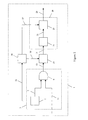
- Figure 2 is a schematic diagram of a circuit for determining when a contact signal has attained a particular stable state indicating that a card is interfaced with the card reader.
- the circuit may be part of a semiconductor integrated circuit that is located, for example, between the card and a micro-controller of a set-top-box, or within the card itself.
- a clock 5 is arranged to generate a periodic clock signal. In the preferred embodiment for example, the clock 5 generates a signal in the form of a one bit digital high pulse every millisecond.
- the clock signal is transmitted via pathway 7 to a first input of an AND gate 9.
- a second input of AND gate 9 receives the contact signal via pathway 11.
- a state signal is transmitted from the output of AND gate 9.
- the state signal is asserted whenever the presence of a high contact signal coincides with the receipt of a clock signal.
- a signal such as the state signal may be asserted by having a particular state such as digital high state.
- a one bit digital high pulse is transmitted from the output of AND gate 9 whenever the presence of a high contact signal coincides with the receipt of a clock signal.
- the state of the contact signal is periodically sampled. For example, in the preferred embodiment, since clock signals are generated every millisecond, the state of the contact signal is sampled every millisecond. Only when the contact signal is sampled as high will a state signal transmitted from AND gate 9 be asserted.
- the state signal output from AND gate 9 is transmitted via pathway 13 to a counter 15.
- the counter 15 has an initial value of zero and is arranged to increment by one each time the state signal on pathway 13 is asserted.
- the value of the counter 15 is caused to be periodically reset to zero by periodic reset signals received by the counter 15 from pathway 16.
- the counter 15 is reset to zero every 64 milliseconds.
- the time period between successive resets of the counter 15 may be referred to as the sampling period.
- the counter 15 thus stores a value that is representative of the number of samples in which the contact signal was sampled as high in the current sampling period.
- the value of counter 15 is transmitted via pathway 17 to a comparator 19.
- the comparator is arranged to output a comparison signal if the value received from the counter 15 is greater than a predetermined threshold.
- the comparator is arranged to output a signal in the form of a one bit pulse only if the value received from the counter 15 is greater than 47.
- the comparison signal output from the comparator 19 is transmitted via pathway 21 to a latch 23.
- the latch 23 also receives periodic latch signals from pathway 27 , each one being received by the latch shortly before the counter 15 is reset.
- the latch 23 is arranged to output a card detection signal upon receipt of a latch signal only if a comparison signal has been received by the latch 23 since the last latch signal.
- a card detection signal is output at the end of a sampling period only if the number of samples in which the contact signal was sampled as high taken within the sampling period exceeded a predetermined threshold.
- the threshold may be considered an absolute value, or as a percentage of the total number of samples within the sampling period.
- a card detection signal in the form of a one bit pulse is output if the contact signal was sampled as high in at least 48 of the samples in the sampling period.
- the clock signal generated by clock 5 is transmitted to a second counter 29 via pathway 31.
- counter 29 is a six bit binary cyclic counter providing for 64 count values.
- the counter 29 is initially set to its minimum value and is arranged to increment by one upon receipt of a clock signal on pathway 31. When counter 29 has reached the maximum value, receipt of a clock signal causes the counter to be reset to the minimum value once again.
- the counter 29 is further arranged to output a first signal on pathway 27 when the counter reaches its maximum value, and to output a second signal on pathway 16 when the counter is reset to the minimum value.
- two signals separated by a millisecond are periodically transmitted from the counter 29 every 64 milliseconds.
- the first signal is the latch signal received by the latch and the second signal is the reset signal that causes counter 15 to be reset.
- the circuit illustrated in Figure 2 causes the state of the contact signal to be sampled once every millisecond in successive sampling periods of 64 milliseconds. At the end of each sampling period, a card detection signal is output if the contact signal was sampled as high on at least 48 of the samples. The counter 15 is then reset and a new set of samples are taken in the next sampling period. This process may be thought of as dividing time into successive 64 millisecond sampling periods and determining the average contact signal during each period (where a low contact signal is considered to have a value of zero and a high contact signal is considered to have a value of one). If the average value for a sampling period exceeds a threshold then the state of the contact signal throughout this period is deemed to be a stable high state for the purpose of card detection.
- the parameters such as the length of the sampling period, the time interval between samples and the threshold are not limited to those values mentioned above.
- samples may be taken every two milliseconds over a sampling period of 80 milliseconds, and the threshold is 60.
- the values of these parameters may be chosen depending on factors including the desired speed at which cards are detected and the stability of card signals that is required.
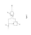
- FIG. 3 shows a schematic representation of a circuit which provides a means for determining whether a card is being inserted into or removed from the card interface.
- the card detection signals transmitted on pathway 25 shown in Figure 2 form a first input of an AND gate 27.
- the card detection signals also form the input of a latch 29.
- the latch 29 Upon receiving an input, the latch 29 is arranged to store the input value and to output a previously stored value. Latch 29 initially stores a low value. The output of the latch 29 is negated and input into the second input of the AND gate 27.
- the card detection signal transmitted on pathway 25 will change from a low value (since no card was previously inserted) to a high value (indicating that a card has been detected).
- a high signal will be transmitted along pathway 25, and the first input of the AND gate 27 will be high.
- the high contact signal will also be input into the latch 29, causing a previously stored low contact signal to be output.
- this low signal becomes high, and the second input of the AND gate 27 is high. In this case, the output of AND gate will be high, indicating that a card has been inserted.
- the card detection signal transmitted on pathway 25 will change from a high value to a low value.
- a low signal will be present on pathway 25 and the first input of the AND gate will be low.
- the low contact signal will also be input into the latch 29, causing the previously stored high contact signal to be output.
- this high signal becomes low, and the second input of the AND gate 27 is low. In this case, the output of AND gate will be low. Therefore the process of removing a card does not result in a signal being output from AND gate 27.
- multiple card interfaces may be provided to enable multiple cards to be used with a single system.
- a circuit illustrated in Figure 2 may be provided for each card interface, so that detection of cards may be performed independently.
- some components may be shared between the interfaces. For example, only a single clock 5 and counter 29 may be provided, with each interface sharing these components. However, other components such as the counter 15 may be provided for each separate interface.
Landscapes
- Engineering & Computer Science (AREA)
- Artificial Intelligence (AREA)
- Computer Vision & Pattern Recognition (AREA)
- Physics & Mathematics (AREA)
- General Physics & Mathematics (AREA)
- Theoretical Computer Science (AREA)
- Electronic Switches (AREA)
- Storage Device Security (AREA)
Priority Applications (3)
| Application Number | Priority Date | Filing Date | Title |
|---|---|---|---|
| DE602004008239T DE602004008239D1 (de) | 2004-06-15 | 2004-06-15 | Kartenerkennung |
| EP04253573A EP1607899B1 (de) | 2004-06-15 | 2004-06-15 | Kartenerkennung |
| US11/152,673 US7506810B2 (en) | 2004-06-15 | 2005-06-14 | Card detection |
Applications Claiming Priority (1)
| Application Number | Priority Date | Filing Date | Title |
|---|---|---|---|
| EP04253573A EP1607899B1 (de) | 2004-06-15 | 2004-06-15 | Kartenerkennung |
Publications (2)
| Publication Number | Publication Date |
|---|---|
| EP1607899A1 true EP1607899A1 (de) | 2005-12-21 |
| EP1607899B1 EP1607899B1 (de) | 2007-08-15 |
Family
ID=34930407
Family Applications (1)
| Application Number | Title | Priority Date | Filing Date |
|---|---|---|---|
| EP04253573A Expired - Lifetime EP1607899B1 (de) | 2004-06-15 | 2004-06-15 | Kartenerkennung |
Country Status (3)
| Country | Link |
|---|---|
| US (1) | US7506810B2 (de) |
| EP (1) | EP1607899B1 (de) |
| DE (1) | DE602004008239D1 (de) |
Cited By (1)
| Publication number | Priority date | Publication date | Assignee | Title |
|---|---|---|---|---|
| US8395407B2 (en) | 2008-06-02 | 2013-03-12 | Sartorius Weighing Technology Gmbh | Electronic device and method for testing a circuit board |
Families Citing this family (5)
| Publication number | Priority date | Publication date | Assignee | Title |
|---|---|---|---|---|
| TWI301574B (en) * | 2005-12-05 | 2008-10-01 | Via Tech Inc | Memory card detect circuit |
| US20090093172A1 (en) * | 2007-10-04 | 2009-04-09 | Chien-Hua Chen | Systems and methods for utilizing single detective pin of host to support plurality of external apparatus |
| TWI463800B (zh) * | 2011-11-22 | 2014-12-01 | Inventec Corp | 除彈跳裝置及其方法 |
| US9680458B1 (en) * | 2016-08-11 | 2017-06-13 | Schweitzer Engineering Laboratories, Inc. | Input-controlled multiple threshold debounce system |
| US10256801B2 (en) | 2016-08-31 | 2019-04-09 | M31 Technology Corporation | Integrated circuit with clock detection and selection function and related method and storage device |
Citations (2)
| Publication number | Priority date | Publication date | Assignee | Title |
|---|---|---|---|---|
| US5912618A (en) * | 1995-12-20 | 1999-06-15 | U.S. Philips Corporation | System for detecting the presence of an electrically conductive object, particularly an integrated circuit on a chip card |
| US20020179707A1 (en) * | 2001-06-04 | 2002-12-05 | Semiconductor Components Industries, Llc. | Smart card reader circuit and insertion detection method |
Family Cites Families (4)
| Publication number | Priority date | Publication date | Assignee | Title |
|---|---|---|---|---|
| US4814591A (en) * | 1987-04-13 | 1989-03-21 | Kabushiki Kaisha Toshiba | Portable medium |
| US5235635A (en) * | 1990-09-27 | 1993-08-10 | Advanced Micro Devices, Inc. | Keypad monitor with keypad activity-based activation |
| WO1995033228A1 (en) * | 1994-05-27 | 1995-12-07 | Elonex Technologies, Inc. | Computer reset signal debouncing circuit |
| GB2437121A (en) * | 2006-04-11 | 2007-10-17 | Wolfson Microelectronics Plc | A debounce circuit with low latency |
-
2004
- 2004-06-15 EP EP04253573A patent/EP1607899B1/de not_active Expired - Lifetime
- 2004-06-15 DE DE602004008239T patent/DE602004008239D1/de not_active Expired - Lifetime
-
2005
- 2005-06-14 US US11/152,673 patent/US7506810B2/en active Active
Patent Citations (2)
| Publication number | Priority date | Publication date | Assignee | Title |
|---|---|---|---|---|
| US5912618A (en) * | 1995-12-20 | 1999-06-15 | U.S. Philips Corporation | System for detecting the presence of an electrically conductive object, particularly an integrated circuit on a chip card |
| US20020179707A1 (en) * | 2001-06-04 | 2002-12-05 | Semiconductor Components Industries, Llc. | Smart card reader circuit and insertion detection method |
Cited By (3)
| Publication number | Priority date | Publication date | Assignee | Title |
|---|---|---|---|---|
| US8395407B2 (en) | 2008-06-02 | 2013-03-12 | Sartorius Weighing Technology Gmbh | Electronic device and method for testing a circuit board |
| US8508236B2 (en) | 2008-06-02 | 2013-08-13 | Sartorius Weighing Technology Gmbh | Electronic device and method for testing a circuit board |
| US8508235B2 (en) | 2008-06-02 | 2013-08-13 | Sartorius Weighing Technology Gmbh | Electronic device and method for testing a circuit board |
Also Published As
| Publication number | Publication date |
|---|---|
| EP1607899B1 (de) | 2007-08-15 |
| US20050284938A1 (en) | 2005-12-29 |
| DE602004008239D1 (de) | 2007-09-27 |
| US7506810B2 (en) | 2009-03-24 |
Similar Documents
| Publication | Publication Date | Title |
|---|---|---|
| US8805905B2 (en) | On-line randomness test for restart random number generators | |
| EP1607899B1 (de) | Kartenerkennung | |
| US20030089774A1 (en) | Apparatus and method for reading magnetic stripes | |
| US6008672A (en) | Input signal reading circuit having a small delay and a high fidelity | |
| US6473841B1 (en) | Signal processing apparatus with memory access history storage | |
| US9319296B2 (en) | Methods for embedding an out-of-band signal into a communication protocol capture stream | |
| EP0301084B1 (de) | Gerät und vorrichtung zur prüfung von kontaktunterbrechungen von schaltungszwischenverbindungen | |
| US20080016082A1 (en) | Memory card detection circuit and method thereof | |
| CN111078118B (zh) | 一种用于对按键进行防抖处理的装置及方法 | |
| US11615049B2 (en) | Programmable serial input-output controller, operation system and method | |
| JPH0823326A (ja) | クロック障害検出回路 | |
| US6473700B1 (en) | Apparatus for use in a logic analyzer for compressing digital data for waveform viewing | |
| CN117054728A (zh) | 时钟丢失检测方法及系统 | |
| CN107168902A (zh) | 一种利用dma实现高速can波特率的自动识别方法 | |
| JP4112874B2 (ja) | コネクタ着脱検出方法およびインタフェース装置 | |
| CN116794552A (zh) | 毛刺检测电路、毛刺检测方法及电子设备 | |
| US8219889B2 (en) | Communication error detection apparatus | |
| US7427879B2 (en) | Frequency detector utilizing pulse generator, and method thereof | |
| KR20190127108A (ko) | Plc의 입력 신호 필터링 장치 | |
| US7970045B2 (en) | Method and device for adapting a signal | |
| JPH03252526A (ja) | センサー出力回路 | |
| KR101192902B1 (ko) | 이동 통신 시스템에서의 동기 검출 방법 및 장치 | |
| JP4381029B2 (ja) | 記憶装置及び記憶制御システム | |
| JP2001282325A (ja) | プログラマブルコントローラ及びこれを用いたコントロールシステム。 | |
| KR100433985B1 (ko) | 마이컴의 노이즈 제거 장치 |
Legal Events
| Date | Code | Title | Description |
|---|---|---|---|
| PUAI | Public reference made under article 153(3) epc to a published international application that has entered the european phase |
Free format text: ORIGINAL CODE: 0009012 |
|
| AK | Designated contracting states |
Kind code of ref document: A1 Designated state(s): AT BE BG CH CY CZ DE DK EE ES FI FR GB GR HU IE IT LI LU MC NL PL PT RO SE SI SK TR |
|
| AX | Request for extension of the european patent |
Extension state: AL HR LT LV MK |
|
| 17P | Request for examination filed |
Effective date: 20060621 |
|
| AKX | Designation fees paid |
Designated state(s): DE FR GB IT |
|
| GRAP | Despatch of communication of intention to grant a patent |
Free format text: ORIGINAL CODE: EPIDOSNIGR1 |
|
| GRAS | Grant fee paid |
Free format text: ORIGINAL CODE: EPIDOSNIGR3 |
|
| GRAA | (expected) grant |
Free format text: ORIGINAL CODE: 0009210 |
|
| AK | Designated contracting states |
Kind code of ref document: B1 Designated state(s): DE FR GB IT |
|
| REG | Reference to a national code |
Ref country code: GB Ref legal event code: FG4D |
|
| REF | Corresponds to: |
Ref document number: 602004008239 Country of ref document: DE Date of ref document: 20070927 Kind code of ref document: P |
|
| ET | Fr: translation filed | ||
| REG | Reference to a national code |
Ref country code: GB Ref legal event code: S117 |
|
| PLBE | No opposition filed within time limit |
Free format text: ORIGINAL CODE: 0009261 |
|
| STAA | Information on the status of an ep patent application or granted ep patent |
Free format text: STATUS: NO OPPOSITION FILED WITHIN TIME LIMIT |
|
| 26N | No opposition filed |
Effective date: 20080516 |
|
| PG25 | Lapsed in a contracting state [announced via postgrant information from national office to epo] |
Ref country code: DE Free format text: LAPSE BECAUSE OF FAILURE TO SUBMIT A TRANSLATION OF THE DESCRIPTION OR TO PAY THE FEE WITHIN THE PRESCRIBED TIME-LIMIT Effective date: 20071116 |
|
| GBPC | Gb: european patent ceased through non-payment of renewal fee |
Effective date: 20080615 |
|
| PG25 | Lapsed in a contracting state [announced via postgrant information from national office to epo] |
Ref country code: GB Free format text: LAPSE BECAUSE OF NON-PAYMENT OF DUE FEES Effective date: 20080615 |
|
| REG | Reference to a national code |
Ref country code: GB Ref legal event code: S28 Free format text: APPLICATION FILED |
|
| REG | Reference to a national code |
Ref country code: GB Ref legal event code: S28 Free format text: RESTORATION ALLOWED Effective date: 20100614 |
|
| PG25 | Lapsed in a contracting state [announced via postgrant information from national office to epo] |
Ref country code: IT Free format text: LAPSE BECAUSE OF NON-PAYMENT OF DUE FEES Effective date: 20080630 |
|
| PGFP | Annual fee paid to national office [announced via postgrant information from national office to epo] |
Ref country code: GB Payment date: 20140527 Year of fee payment: 11 |
|
| REG | Reference to a national code |
Ref country code: GB Ref legal event code: S117 Free format text: CORRECTIONS ALLOWED; REQUEST FOR CORRECTION UNDER SECTION 117 FILED ON 03 APRIL 2008 ALLOWED ON 21 AUGUST 2014. |
|
| GBPC | Gb: european patent ceased through non-payment of renewal fee |
Effective date: 20150615 |
|
| PG25 | Lapsed in a contracting state [announced via postgrant information from national office to epo] |
Ref country code: GB Free format text: LAPSE BECAUSE OF NON-PAYMENT OF DUE FEES Effective date: 20150615 |
|
| REG | Reference to a national code |
Ref country code: FR Ref legal event code: PLFP Year of fee payment: 13 |
|
| REG | Reference to a national code |
Ref country code: FR Ref legal event code: PLFP Year of fee payment: 14 |
|
| REG | Reference to a national code |
Ref country code: FR Ref legal event code: TP Owner name: STMICROELECTRONICS (RESEARCH & DEVELOPMENT) LI, GB Effective date: 20180105 |
|
| REG | Reference to a national code |
Ref country code: FR Ref legal event code: PLFP Year of fee payment: 15 |
|
| PGFP | Annual fee paid to national office [announced via postgrant information from national office to epo] |
Ref country code: FR Payment date: 20200520 Year of fee payment: 17 |
|
| PG25 | Lapsed in a contracting state [announced via postgrant information from national office to epo] |
Ref country code: FR Free format text: LAPSE BECAUSE OF NON-PAYMENT OF DUE FEES Effective date: 20210630 |