EP1606885B1 - Digital pulse width controlled oscillation modulator - Google Patents
Digital pulse width controlled oscillation modulator Download PDFInfo
- Publication number
- EP1606885B1 EP1606885B1 EP04722600A EP04722600A EP1606885B1 EP 1606885 B1 EP1606885 B1 EP 1606885B1 EP 04722600 A EP04722600 A EP 04722600A EP 04722600 A EP04722600 A EP 04722600A EP 1606885 B1 EP1606885 B1 EP 1606885B1
- Authority
- EP
- European Patent Office
- Prior art keywords
- modulator
- integrator
- output
- comparator
- filter
- Prior art date
- Legal status (The legal status is an assumption and is not a legal conclusion. Google has not performed a legal analysis and makes no representation as to the accuracy of the status listed.)
- Expired - Lifetime
Links
- 230000010355 oscillation Effects 0.000 title claims description 20
- 238000013139 quantization Methods 0.000 claims abstract description 14
- 238000006243 chemical reaction Methods 0.000 claims description 12
- 230000005540 biological transmission Effects 0.000 claims description 2
- 230000006870 function Effects 0.000 description 16
- 238000010586 diagram Methods 0.000 description 9
- 230000004044 response Effects 0.000 description 8
- 230000035945 sensitivity Effects 0.000 description 6
- 238000007493 shaping process Methods 0.000 description 3
- 230000003321 amplification Effects 0.000 description 2
- 238000001914 filtration Methods 0.000 description 2
- 238000003199 nucleic acid amplification method Methods 0.000 description 2
- XUIMIQQOPSSXEZ-UHFFFAOYSA-N Silicon Chemical compound [Si] XUIMIQQOPSSXEZ-UHFFFAOYSA-N 0.000 description 1
- 230000001419 dependent effect Effects 0.000 description 1
- 230000000694 effects Effects 0.000 description 1
- 230000005520 electrodynamics Effects 0.000 description 1
- 230000008030 elimination Effects 0.000 description 1
- 238000003379 elimination reaction Methods 0.000 description 1
- 238000005516 engineering process Methods 0.000 description 1
- 238000000034 method Methods 0.000 description 1
- 230000000630 rising effect Effects 0.000 description 1
- 238000005070 sampling Methods 0.000 description 1
- 229910052710 silicon Inorganic materials 0.000 description 1
- 239000010703 silicon Substances 0.000 description 1
- 230000005236 sound signal Effects 0.000 description 1
- 230000001629 suppression Effects 0.000 description 1
- 230000001360 synchronised effect Effects 0.000 description 1
Images


Classifications
-
- H—ELECTRICITY
- H03—ELECTRONIC CIRCUITRY
- H03M—CODING; DECODING; CODE CONVERSION IN GENERAL
- H03M5/00—Conversion of the form of the representation of individual digits
- H03M5/02—Conversion to or from representation by pulses
- H03M5/04—Conversion to or from representation by pulses the pulses having two levels
- H03M5/06—Code representation, e.g. transition, for a given bit cell depending only on the information in that bit cell
- H03M5/08—Code representation by pulse width
-
- H—ELECTRICITY
- H03—ELECTRONIC CIRCUITRY
- H03M—CODING; DECODING; CODE CONVERSION IN GENERAL
- H03M3/00—Conversion of analogue values to or from differential modulation
- H03M3/30—Delta-sigma modulation
- H03M3/50—Digital/analogue converters using delta-sigma modulation as an intermediate step
- H03M3/502—Details of the final digital/analogue conversion following the digital delta-sigma modulation
- H03M3/506—Details of the final digital/analogue conversion following the digital delta-sigma modulation the final digital/analogue converter being constituted by a pulse width modulator
-
- H—ELECTRICITY
- H03—ELECTRONIC CIRCUITRY
- H03M—CODING; DECODING; CODE CONVERSION IN GENERAL
- H03M7/00—Conversion of a code where information is represented by a given sequence or number of digits to a code where the same, similar or subset of information is represented by a different sequence or number of digits
- H03M7/30—Compression; Expansion; Suppression of unnecessary data, e.g. redundancy reduction
- H03M7/3002—Conversion to or from differential modulation
- H03M7/3004—Digital delta-sigma modulation
- H03M7/3015—Structural details of digital delta-sigma modulators
- H03M7/302—Structural details of digital delta-sigma modulators characterised by the number of quantisers and their type and resolution
- H03M7/3024—Structural details of digital delta-sigma modulators characterised by the number of quantisers and their type and resolution having one quantiser only
- H03M7/3028—Structural details of digital delta-sigma modulators characterised by the number of quantisers and their type and resolution having one quantiser only the quantiser being a single bit one
-
- H—ELECTRICITY
- H03—ELECTRONIC CIRCUITRY
- H03M—CODING; DECODING; CODE CONVERSION IN GENERAL
- H03M7/00—Conversion of a code where information is represented by a given sequence or number of digits to a code where the same, similar or subset of information is represented by a different sequence or number of digits
- H03M7/30—Compression; Expansion; Suppression of unnecessary data, e.g. redundancy reduction
- H03M7/3002—Conversion to or from differential modulation
- H03M7/3004—Digital delta-sigma modulation
- H03M7/3015—Structural details of digital delta-sigma modulators
- H03M7/3031—Structural details of digital delta-sigma modulators characterised by the order of the loop filter, e.g. having a first order loop filter in the feedforward path
- H03M7/3033—Structural details of digital delta-sigma modulators characterised by the order of the loop filter, e.g. having a first order loop filter in the feedforward path the modulator having a higher order loop filter in the feedforward path, e.g. with distributed feedforward inputs
- H03M7/304—Structural details of digital delta-sigma modulators characterised by the order of the loop filter, e.g. having a first order loop filter in the feedforward path the modulator having a higher order loop filter in the feedforward path, e.g. with distributed feedforward inputs with distributed feedback, i.e. with feedback paths from the quantiser output to more than one filter stage
Definitions
- the present invention relates in general to a digital pulse width modulator, and to a power conversion system implementing such a modulator. More specifically, the invention relates to a system for conversion of sampled digital signals such as Pulse Code Modulated (PCM) signals to a Pulse Width Modulated (PWM) signal, also known as PCM-PWM conversion.
- PCM Pulse Code Modulated
- PWM Pulse Width Modulated
- Prior art digital PWM modulators generate a pulse width modulated signal with a carrier frequency of minimum twice the signal frequency to comply with the Nyquist criteria.
- the objective for such a system implementation is to achieve noise and distortion artifacts lower than quantization noise of the sampled signals, which is a challenging task when operating with sampled audio signals of 24 bit resolution. The result is a complex and expensive system.
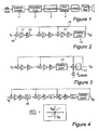
- Such a system is illustrated in fig 1 , and comprises a sample rate converter 1, an oversampler 2, a noise shaper 4 and an error correcting algorithm unit 3.
- the carrier frequency is dependent on the sample frequency, making the use of a sample rate converter 1 necessary.
- sample rate conversion becomes mandatory.
- the sample rate converter 1 can be complex to implement due to high order filtering. Quantization errors and aliasing will be introduced leading to reduced dynamic ranges.
- an error correcting algorithm 3 and a noise shaper 4 must be comprised in the design leading to unnecessary complexity and cost.
- the noise shaper 3 is limited in bandwidth, as the maximum loop gain to suppress the quantization noise is constrained by the stability of the noise shaping loop. Therefore, the noise shaper 4 does still not achieve a satisfactory dynamic range.
- Analog PWM modulators where an analog input signal is converted into a PWM signal is also known from prior art systems.
- prior art systems In order to obtain a stable system and shape the control loop characteristics, such prior art systems often require additional lead-, lag, lead-lag or lag-lead compensators in the control structure.
- the object of the present invention is to overcome or at least mitigate the above problems, and provide a non-complex system capable of receiving a sampled digital input signal and converting it to PWM domain.
- a pulse width modulator comprising a plurality of integrators with integrator gains arranged in series, a comparator for comparing the output of the last integrator with a reference, and thereby creating the PWM signal, means for realizing self-oscillation at a desired switching frequency, and a feedback path connected to a point down stream said comparator and leading to a plurality of summing points, each preceding one of said integrators.
- the PWM signal is quantized in time by the clock frequency of the modulator, and the integrator gains are adapted to reduce any quantization noise.
- the loop gain is thus set to reduce the noise generated by quantization in the system.
- the system can provide an improved loop gain bandwidth corresponding to the switching frequency, leading to much wider control bandwidths compared to prior art systems. This leads to even higher suppression of noise and distortion components within the modulator bandwidth, since the ratio between the switching frequency and the modulator bandwidth can be less than in prior art systems.
- quantization noise has been mentioned specifically, it is clear that any noise introduced into the modulator will be reduced by the invention.
- the noise can be reduced to levels corresponding to the resolution of the digital input signal, typically a 24-bit signal.
- the effect of the multiple feedback loop and the integrators with gain is similar to that of the noise shaper of prior art, but the self-oscillating nature of the system has the benefit of higher loop gain in the modulator loop compared to what can be obtained by a noise shaper.
- the obtainable dynamic range is therefore higher than prior art, and at the same time the use of noise shapers is eliminated.
- the modulator is independent of the format of the input signal, especially regarding the sampling frequency, the modulator according to the invention need not to be synchronized with the signal source. This is of great benefit and eliminates the use of prior art sample rate converters and oversamplers.
- a modulator according to the invention can be implemented on less than 10% of the silicon area required for a prior art modulator. Efficiency is improved and cost is reduced dramatically.
- the modulator according to the invention further provides a carrier frequency (equal to the switching frequency) which varies with the modulation index.
- a carrier frequency equal to the switching frequency
- VFPWM Variable carrier Frequency Pulse Width Modulation
- the feedback path is connected directly to the output of the comparator. This results in a modulator that is functionally separated from any switching stage amplification or other elements supplied with the PWM signal.
- the integrator gains can be selected so that the system transfer function is a low pass filter, where the loop gain is equal to the mirrored frequency response around the cut-off frequency. Such a design is particularly advantageous for audio implementations.
- the system transfer function can be implemented as a Bessel or Butterworth low-pass filter.
- These filter implementations provide very suitable frequency characteristics and sensitivity functions which will provide a stabile and very robust system. Furthermore it will be easy to shape the overall system characteristics.
- G n G n - 1 2 M
- M M ⁇ [0, ⁇ ]
- a signal amplitude limiter can be provided following each integrator gain, preferably with a limitation corresponding to a dynamic range of the input signal.
- the amplitude limiters serve to stabilize the feedback loops in the case of aggressive loop implementations, implemented to achieve high performance with very few integrators.
- the self-oscillation can be achieved with a positive feedback of the comparator.
- This design results in a hysteresis loop which brings the system to a controlled oscillation and hereby generates the modulator carrier signal.
- the switching frequency is determined by the integrator gain immediately preceding the comparator.
- the self-oscillation can alternatively be achieved by a filter or time delay preceding the comparator, said filter or time delay being arranged to give the system an open loop phase lag of 180 degrees at the desired switching frequency.
- the phase-lag will result in a non-hysteresis oscillation, thus generating the modulator carrier signal.
- a second aspect of the invention is a power conversion system comprising a modulator according the first aspect of the invention, a switching stage connected to the oscillation control, and an output filter connected to the switching stage.
- Such a power converter is very suitable in all types of precision DC-AC conversion applications such as audio amplification, motor or electro-dynamic transducer drive applications or line drivers for line transmission.
- Fig 2 is a general block diagram of a modulator 10 according to a first preferred embodiment of the invention.
- the modulator comprises a chain of serially connected integrators 11, with associated integrator gains 12, the output of this chain being connected to an oscillation control 13.
- the integrator gains 12 are shown as separate elements. In practice, and as will be shown with reference to fig 7 , the integrator has an inherent gain, and then an additional adjustment of this gain is provided. The adjustment can very well be an attenuation of the integrator gain.
- the oscillation control 13 is arranged to cause self-oscillation of the modulator, and includes a comparator 17, (see figs 5 and 6 ) for comparing the output of the last integrator 11' in the integrator chain with a reference.
- the comparator 17 is a simple sign detector, in which case the reference is the ground level.
- the result of this comparison is the PWM signal, which can be supplied to a switching amplifier power stage, as illustrated in fig 8 .
- a feedback path 14 is connected to a point downstream the oscillation control, and arranged to provide a negative feedback signal to summation points 15 provided immediately preceding each integrator 11.
- the system is implemented as a general N'th order lowpass system by selecting the integrator gains 12 in a suitable way, where the number of integrators N equals the order of the system.
- the output carrier is created by deliberately causing the loop to be unstable, and the resulting oscillation frequency is the carrier frequency, typically in the area of 500KHz.
- the generation of the PWM signal is quantized in time by the clock frequency of the digital system, typically in the area of 100-200MHz. With a carrier (switching) frequency of around 500 kHz, this gives a time resolution of each carrier cycle of around 200-400, or 7-9 bits. This quantization results in quantization noise in the same way as in the case of the oversampler of prior art.
- Fig 3 illustrates schematically how the quantization noise is introduced into the system.
- the quantization noise can be suppressed to an almost infinitesimal level in the total audio band.
- voltage limiters can be provided on the output of each integrator gain 12.
- Fig 5 illustrates how the oscillation control 13 in fig 2 can be implemented as a hysteresis control 13a.
- a positive feedback 16 is provided from the output of the comparator 17 to a summation point 18 preceding the comparator.
- O(s) 1.
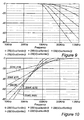
- the transfer function is a general low pass function, and by adjusting the integrator gains the pole configuration can be set to form for example a Butterworth or Bessel filter characteristic.
- the diagram shows the reduction of the quantization noise and other distortion components. For example, for a fifth order system, any errors will be reduced with up to 69 dB at 20 KHz.
- Fig 6 illustrates how the oscillation control 13 in fig 2 can be implemented as a non-hysteresis control 13b.
- the oscillation control 13b now includes a control block 20 for creating an open loop phase lag.
- the self-oscillation can be achieved by providing phase lag of 180 degrees or a delay corresponding to a 180-degree phase lag at the preferred carrier frequency.
- the purpose of this control block 20 is thus to provide the necessary phase lag for bringing the loop into oscillation, and this can be accomplished by using pure delay, integrating functions or local filter systems.
- the control block 20 in fig 6 is a local filter O(s) of a general all pass filter type. This filter type is preferred because it has an absolute gain of 1, which means that this implementation has the same transfer function H(s) as the hysteresis system (see Eq. 1).
- the different implementations ( figs 5 and 6 ) of the oscillation control 13a, 13b have equal system performance. However, an additional P integrators will be required for the filter 20 in the case of the non-hysteresis approach, for the same performance.
- the loop gain is determined by the number of integrators in the global loop.
- the benefit of a non-hysteresis control ( fig 4 ) is the possibility of a very steep phase characteristic around the carrier frequency to achieve low variation of the carrier frequency as function of the modulation index. This property can be valuable in some applications.
- the integrator gains are selected to have a ratio of a multiple of 2.
- Fig 7 shows a more detailed implementation of a 2:nd order modulator according to fig 5 , using the above described shifting technique for achieving the gains.
- the summing point 18 and comparator 17 in fig 3 are embodied by an adder 21, having a sign bit output 22.
- the output 22 has signal levels of ⁇ V, where V is the peak value of the PWM signal.
- the summation points 15 in fig 5 are further embodied by two adders 23a, 23b, and the integrators 11 in fig 5 are embodied by two adders 24a, 24b.
- the integrator gains 12 in fig 5 are embodied partly by the gain of the adders 24a, 24b, and partly by two shifting registers 25a, 25b.
- the shifting registers 25a, 25b act to adjust the gain of the adders 24a, 24b to achieve the desired filtering.
- the adjustment can be performed by shifting right, i.e. attenuating the gain of the adders 24a, 24b.
- the first shifting register 25a which is the gain immediately preceding the comparator 21, can be arranged to perform one shifting operation less than the register 25b, in order to realize a first integrator gain G 1 equal to twice the second integrator gain G 2 .
- further gain coefficients according to e.g. fig 12 may be accomplished by further adders and shifting registers.
- the modulator further has a feedback path 26 connected to the output 22 of the adder 21.
- This feedback 26 has two separate objectives: Firstly, it provides an oscillation control by providing a feedback 27 to itself. This corresponds to the hysteresis control loop 16 in fig 5 . Secondly, it provides a feedback 28 of the output 22 to the two adders 23a, 23b, corresponding to the multiple feedback loop 14 in fig 5 .
- An interface block 29 is arranged to receive a serial data stream and placing a sample in a parallel register, here a 24-bit register, which is connected to the adder 23b.
- Synchronization of one or a plurality of modulators can be achieved by applying phase lock loops 30 to each of the modulators. Thereby synchronization can be obtained by phase control of the modulators.
- a preferred embodiment of a power converter according to the invention is shown in fig 8 , where a switching output power stage 31 is provided to the modulator 10 as shown in fig 2 .
- the switching signal is filtered in an output filter 32, and connected to a load 33, e.g. an audio speaker.
- the feedback path 14 is moved down stream, and is connected to the output of the switching stage 31.
- the benefit of this approach is to reduce the errors added by the output stage such as blanking delay errors.
- the THD and noise introduced by the output stage will be multiplied by the sensitivity function and therefore brought to a very low level.
- a feedback instead can be applied from the output filter 32 by adding compensation of at least N-1 poles of the output filter 32, where N is the order of the filter.
- the invention can advantageously be used in any digital to analog conversion systems also where high dynamic range and high linearity are required as e.g. audio systems and in particular in switching power amplifiers for audio use or any other power conversion system. Further, the invention can be used for general D/A conversion.
Landscapes
- Engineering & Computer Science (AREA)
- Theoretical Computer Science (AREA)
- Amplifiers (AREA)
- Compression, Expansion, Code Conversion, And Decoders (AREA)
- Dc-Dc Converters (AREA)
- Analogue/Digital Conversion (AREA)
- Preparation Of Compounds By Using Micro-Organisms (AREA)
- Medicines Containing Plant Substances (AREA)
Applications Claiming Priority (3)
| Application Number | Priority Date | Filing Date | Title |
|---|---|---|---|
| SE0300780 | 2003-03-24 | ||
| SE0300780A SE0300780D0 (sv) | 2003-03-24 | 2003-03-24 | Digital pulse width controlled oscillation modulator |
| PCT/IB2004/000852 WO2004086629A1 (en) | 2003-03-24 | 2004-03-23 | Digital pulse width controlled oscillation modulator |
Publications (2)
| Publication Number | Publication Date |
|---|---|
| EP1606885A1 EP1606885A1 (en) | 2005-12-21 |
| EP1606885B1 true EP1606885B1 (en) | 2009-02-11 |
Family
ID=20290741
Family Applications (1)
| Application Number | Title | Priority Date | Filing Date |
|---|---|---|---|
| EP04722600A Expired - Lifetime EP1606885B1 (en) | 2003-03-24 | 2004-03-23 | Digital pulse width controlled oscillation modulator |
Country Status (12)
| Country | Link |
|---|---|
| US (1) | US7479840B2 (enExample) |
| EP (1) | EP1606885B1 (enExample) |
| JP (1) | JP4477623B2 (enExample) |
| KR (1) | KR101076636B1 (enExample) |
| CN (1) | CN1765055B (enExample) |
| AT (1) | ATE422730T1 (enExample) |
| AU (1) | AU2004223010B2 (enExample) |
| CA (1) | CA2519884A1 (enExample) |
| DE (1) | DE602004019401D1 (enExample) |
| ES (1) | ES2319423T3 (enExample) |
| SE (1) | SE0300780D0 (enExample) |
| WO (1) | WO2004086629A1 (enExample) |
Families Citing this family (10)
| Publication number | Priority date | Publication date | Assignee | Title |
|---|---|---|---|---|
| WO2007098766A1 (en) * | 2006-03-01 | 2007-09-07 | Danmarks Teknishe Universitet | Digital self-oscillating modulator |
| US7868803B2 (en) * | 2006-10-13 | 2011-01-11 | Panasonic Corporation | Semiconductor device having ΔΣ modulator, and semiconductor system |
| US7714675B2 (en) * | 2006-12-05 | 2010-05-11 | Broadcom Corporation | All digital Class-D modulator and its saturation protection techniques |
| KR100963847B1 (ko) * | 2008-02-12 | 2010-06-16 | 주식회사 씨자인 | 교차 입력신호 변조기 |
| TW201015863A (en) * | 2008-10-07 | 2010-04-16 | Unisonic Technologies Co Ltd | PWM control circuit using city power-line electricity frequency modulation to reduce electromagnetic interference and method thereof |
| JP5413216B2 (ja) * | 2010-01-25 | 2014-02-12 | 富士通株式会社 | 遅延時間差測定回路 |
| US8081041B2 (en) * | 2010-02-19 | 2011-12-20 | Exar Corporation | Glue-logic based method and system for minimizing losses in oversampled digitally controlled DC-DC converters |
| CN110850923B (zh) | 2014-05-22 | 2022-05-13 | 德克萨斯仪器股份有限公司 | 具有双计数器数字积分器的直流到直流转换器控制器装置 |
| EP3416285B1 (en) * | 2017-06-16 | 2021-06-02 | ICEpower a/s | Self-oscillating amplifier system |
| KR102905493B1 (ko) * | 2019-12-26 | 2025-12-29 | 시냅틱스 인코포레이티드 | 저 지연, 저 전력 및 고 선형성 클래스-d 변조 루프 |
Family Cites Families (8)
| Publication number | Priority date | Publication date | Assignee | Title |
|---|---|---|---|---|
| JPH05304475A (ja) * | 1992-04-10 | 1993-11-16 | Nec Corp | ノイズシェイパ |
| ATE366483T1 (de) | 1996-03-28 | 2007-07-15 | Texas Instr Denmark As | Umwandlung eines pcm-signals in ein gleichmässig pulsbreitenmoduliertes signal |
| US5777512A (en) * | 1996-06-20 | 1998-07-07 | Tripath Technology, Inc. | Method and apparatus for oversampled, noise-shaping, mixed-signal processing |
| US5886586A (en) * | 1996-09-06 | 1999-03-23 | The Regents Of The University Of California | General constant frequency pulse-width modulators |
| EP1042865B8 (en) * | 1997-04-02 | 2005-01-19 | Bang & Olufsen Icepower A/S | Pulse referenced control method for enhanced power amplification of a pulse modulated signal |
| US6390579B1 (en) * | 1999-04-15 | 2002-05-21 | Hewlett-Packard Company | Pulse width modulator using delay-line technology with automatic calibration of delays to desired operating frequency |
| SE0003342D0 (sv) * | 2000-09-19 | 2000-09-19 | Bang & Olufsen Powerhouse As | Controlled self-oscillation modulator and power conversion system using such a modulator |
| GB0110340D0 (en) * | 2001-04-27 | 2001-06-20 | Watts Robert D | A signal processing circuit |
-
2003
- 2003-03-24 SE SE0300780A patent/SE0300780D0/xx unknown
-
2004
- 2004-03-23 KR KR1020057017984A patent/KR101076636B1/ko not_active Expired - Fee Related
- 2004-03-23 AU AU2004223010A patent/AU2004223010B2/en not_active Ceased
- 2004-03-23 WO PCT/IB2004/000852 patent/WO2004086629A1/en not_active Ceased
- 2004-03-23 CA CA002519884A patent/CA2519884A1/en not_active Abandoned
- 2004-03-23 CN CN2004800079817A patent/CN1765055B/zh not_active Expired - Fee Related
- 2004-03-23 JP JP2006506372A patent/JP4477623B2/ja not_active Expired - Fee Related
- 2004-03-23 EP EP04722600A patent/EP1606885B1/en not_active Expired - Lifetime
- 2004-03-23 ES ES04722600T patent/ES2319423T3/es not_active Expired - Lifetime
- 2004-03-23 US US10/548,432 patent/US7479840B2/en not_active Expired - Fee Related
- 2004-03-23 DE DE602004019401T patent/DE602004019401D1/de not_active Expired - Lifetime
- 2004-03-23 AT AT04722600T patent/ATE422730T1/de not_active IP Right Cessation
Also Published As
| Publication number | Publication date |
|---|---|
| KR20060005346A (ko) | 2006-01-17 |
| EP1606885A1 (en) | 2005-12-21 |
| CA2519884A1 (en) | 2004-10-07 |
| WO2004086629A1 (en) | 2004-10-07 |
| US20060232351A1 (en) | 2006-10-19 |
| US7479840B2 (en) | 2009-01-20 |
| AU2004223010A1 (en) | 2004-10-07 |
| JP4477623B2 (ja) | 2010-06-09 |
| AU2004223010B2 (en) | 2006-12-07 |
| ATE422730T1 (de) | 2009-02-15 |
| JP2006521736A (ja) | 2006-09-21 |
| KR101076636B1 (ko) | 2011-10-26 |
| ES2319423T3 (es) | 2009-05-07 |
| CN1765055B (zh) | 2012-01-11 |
| DE602004019401D1 (de) | 2009-03-26 |
| CN1765055A (zh) | 2006-04-26 |
| SE0300780D0 (sv) | 2003-03-24 |
Similar Documents
| Publication | Publication Date | Title |
|---|---|---|
| US7058464B2 (en) | Device and method for signal processing | |
| US7612608B2 (en) | Sigma-delta based Class D audio or servo amplifier with load noise shaping | |
| EP1653604B1 (en) | Switching power amplifier and method for amplifying a digital input signal | |
| US7605653B2 (en) | Sigma-delta based class D audio power amplifier with high power efficiency | |
| WO2002099966A1 (en) | Switching amplifier having digital correction and method therefor | |
| US7317413B2 (en) | Multi-channel digital to analog (D/A) conversion | |
| US7479840B2 (en) | Digital pulse width controlled oscillation modulator | |
| TWI504161B (zh) | 數位類比轉換系統與方法 | |
| US7170360B2 (en) | Device and method for digital pulse width modulation | |
| US20080278209A1 (en) | Method of pulse width modulation signal processing and device including signal processing for pulse width modulation | |
| US8698662B2 (en) | System and method for a high resolution digital input class D amplifier with feedback | |
| EP1653605B1 (en) | Noise shaper for shaping a power spectral density of an error signal and method therefor | |
| US9431973B2 (en) | Pulse-width modulation generator | |
| JP4660778B2 (ja) | Pwm信号生成器、pwm信号生成装置およびデジタルアンプ | |
| US8698661B2 (en) | System and method for pulse width modulation digital-to-analog converter | |
| EP1813015B1 (en) | Arrangement for amplifying a pwm input signal | |
| JP2006222660A (ja) | A/d変換器、d/a変換器及び伝送装置 |
Legal Events
| Date | Code | Title | Description |
|---|---|---|---|
| PUAI | Public reference made under article 153(3) epc to a published international application that has entered the european phase |
Free format text: ORIGINAL CODE: 0009012 |
|
| 17P | Request for examination filed |
Effective date: 20050922 |
|
| AK | Designated contracting states |
Kind code of ref document: A1 Designated state(s): AT BE BG CH CY CZ DE DK EE ES FI FR GB GR HU IE IT LI LU MC NL PL PT RO SE SI SK TR |
|
| AX | Request for extension of the european patent |
Extension state: AL LT LV MK |
|
| DAX | Request for extension of the european patent (deleted) | ||
| 17Q | First examination report despatched |
Effective date: 20061120 |
|
| GRAP | Despatch of communication of intention to grant a patent |
Free format text: ORIGINAL CODE: EPIDOSNIGR1 |
|
| GRAS | Grant fee paid |
Free format text: ORIGINAL CODE: EPIDOSNIGR3 |
|
| GRAA | (expected) grant |
Free format text: ORIGINAL CODE: 0009210 |
|
| AK | Designated contracting states |
Kind code of ref document: B1 Designated state(s): AT BE BG CH CY CZ DE DK EE ES FI FR GB GR HU IE IT LI LU MC NL PL PT RO SE SI SK TR |
|
| REG | Reference to a national code |
Ref country code: GB Ref legal event code: FG4D |
|
| REG | Reference to a national code |
Ref country code: CH Ref legal event code: EP |
|
| REG | Reference to a national code |
Ref country code: IE Ref legal event code: FG4D |
|
| REF | Corresponds to: |
Ref document number: 602004019401 Country of ref document: DE Date of ref document: 20090326 Kind code of ref document: P |
|
| REG | Reference to a national code |
Ref country code: ES Ref legal event code: FG2A Ref document number: 2319423 Country of ref document: ES Kind code of ref document: T3 |
|
| PG25 | Lapsed in a contracting state [announced via postgrant information from national office to epo] |
Ref country code: FI Free format text: LAPSE BECAUSE OF FAILURE TO SUBMIT A TRANSLATION OF THE DESCRIPTION OR TO PAY THE FEE WITHIN THE PRESCRIBED TIME-LIMIT Effective date: 20090211 Ref country code: SI Free format text: LAPSE BECAUSE OF FAILURE TO SUBMIT A TRANSLATION OF THE DESCRIPTION OR TO PAY THE FEE WITHIN THE PRESCRIBED TIME-LIMIT Effective date: 20090211 |
|
| PG25 | Lapsed in a contracting state [announced via postgrant information from national office to epo] |
Ref country code: SE Free format text: LAPSE BECAUSE OF FAILURE TO SUBMIT A TRANSLATION OF THE DESCRIPTION OR TO PAY THE FEE WITHIN THE PRESCRIBED TIME-LIMIT Effective date: 20090511 Ref country code: PL Free format text: LAPSE BECAUSE OF FAILURE TO SUBMIT A TRANSLATION OF THE DESCRIPTION OR TO PAY THE FEE WITHIN THE PRESCRIBED TIME-LIMIT Effective date: 20090211 Ref country code: AT Free format text: LAPSE BECAUSE OF FAILURE TO SUBMIT A TRANSLATION OF THE DESCRIPTION OR TO PAY THE FEE WITHIN THE PRESCRIBED TIME-LIMIT Effective date: 20090211 |
|
| PG25 | Lapsed in a contracting state [announced via postgrant information from national office to epo] |
Ref country code: BE Free format text: LAPSE BECAUSE OF FAILURE TO SUBMIT A TRANSLATION OF THE DESCRIPTION OR TO PAY THE FEE WITHIN THE PRESCRIBED TIME-LIMIT Effective date: 20090211 |
|
| PG25 | Lapsed in a contracting state [announced via postgrant information from national office to epo] |
Ref country code: EE Free format text: LAPSE BECAUSE OF FAILURE TO SUBMIT A TRANSLATION OF THE DESCRIPTION OR TO PAY THE FEE WITHIN THE PRESCRIBED TIME-LIMIT Effective date: 20090211 Ref country code: DK Free format text: LAPSE BECAUSE OF FAILURE TO SUBMIT A TRANSLATION OF THE DESCRIPTION OR TO PAY THE FEE WITHIN THE PRESCRIBED TIME-LIMIT Effective date: 20090211 Ref country code: CZ Free format text: LAPSE BECAUSE OF FAILURE TO SUBMIT A TRANSLATION OF THE DESCRIPTION OR TO PAY THE FEE WITHIN THE PRESCRIBED TIME-LIMIT Effective date: 20090211 Ref country code: PT Free format text: LAPSE BECAUSE OF FAILURE TO SUBMIT A TRANSLATION OF THE DESCRIPTION OR TO PAY THE FEE WITHIN THE PRESCRIBED TIME-LIMIT Effective date: 20090713 Ref country code: MC Free format text: LAPSE BECAUSE OF NON-PAYMENT OF DUE FEES Effective date: 20090331 |
|
| REG | Reference to a national code |
Ref country code: CH Ref legal event code: PL |
|
| PG25 | Lapsed in a contracting state [announced via postgrant information from national office to epo] |
Ref country code: RO Free format text: LAPSE BECAUSE OF FAILURE TO SUBMIT A TRANSLATION OF THE DESCRIPTION OR TO PAY THE FEE WITHIN THE PRESCRIBED TIME-LIMIT Effective date: 20090211 Ref country code: SK Free format text: LAPSE BECAUSE OF FAILURE TO SUBMIT A TRANSLATION OF THE DESCRIPTION OR TO PAY THE FEE WITHIN THE PRESCRIBED TIME-LIMIT Effective date: 20090211 |
|
| PLBE | No opposition filed within time limit |
Free format text: ORIGINAL CODE: 0009261 |
|
| STAA | Information on the status of an ep patent application or granted ep patent |
Free format text: STATUS: NO OPPOSITION FILED WITHIN TIME LIMIT |
|
| REG | Reference to a national code |
Ref country code: IE Ref legal event code: MM4A |
|
| 26N | No opposition filed |
Effective date: 20091112 |
|
| PG25 | Lapsed in a contracting state [announced via postgrant information from national office to epo] |
Ref country code: BG Free format text: LAPSE BECAUSE OF FAILURE TO SUBMIT A TRANSLATION OF THE DESCRIPTION OR TO PAY THE FEE WITHIN THE PRESCRIBED TIME-LIMIT Effective date: 20090511 Ref country code: LI Free format text: LAPSE BECAUSE OF NON-PAYMENT OF DUE FEES Effective date: 20090331 Ref country code: IE Free format text: LAPSE BECAUSE OF NON-PAYMENT OF DUE FEES Effective date: 20090323 Ref country code: CH Free format text: LAPSE BECAUSE OF NON-PAYMENT OF DUE FEES Effective date: 20090331 |
|
| PG25 | Lapsed in a contracting state [announced via postgrant information from national office to epo] |
Ref country code: GR Free format text: LAPSE BECAUSE OF FAILURE TO SUBMIT A TRANSLATION OF THE DESCRIPTION OR TO PAY THE FEE WITHIN THE PRESCRIBED TIME-LIMIT Effective date: 20090512 |
|
| PG25 | Lapsed in a contracting state [announced via postgrant information from national office to epo] |
Ref country code: LU Free format text: LAPSE BECAUSE OF NON-PAYMENT OF DUE FEES Effective date: 20090323 |
|
| PG25 | Lapsed in a contracting state [announced via postgrant information from national office to epo] |
Ref country code: HU Free format text: LAPSE BECAUSE OF FAILURE TO SUBMIT A TRANSLATION OF THE DESCRIPTION OR TO PAY THE FEE WITHIN THE PRESCRIBED TIME-LIMIT Effective date: 20090812 |
|
| PG25 | Lapsed in a contracting state [announced via postgrant information from national office to epo] |
Ref country code: TR Free format text: LAPSE BECAUSE OF FAILURE TO SUBMIT A TRANSLATION OF THE DESCRIPTION OR TO PAY THE FEE WITHIN THE PRESCRIBED TIME-LIMIT Effective date: 20090211 |
|
| PG25 | Lapsed in a contracting state [announced via postgrant information from national office to epo] |
Ref country code: CY Free format text: LAPSE BECAUSE OF FAILURE TO SUBMIT A TRANSLATION OF THE DESCRIPTION OR TO PAY THE FEE WITHIN THE PRESCRIBED TIME-LIMIT Effective date: 20090211 |
|
| REG | Reference to a national code |
Ref country code: FR Ref legal event code: PLFP Year of fee payment: 12 |
|
| PGFP | Annual fee paid to national office [announced via postgrant information from national office to epo] |
Ref country code: DE Payment date: 20150304 Year of fee payment: 12 Ref country code: ES Payment date: 20150324 Year of fee payment: 12 Ref country code: IT Payment date: 20150316 Year of fee payment: 12 Ref country code: NL Payment date: 20150303 Year of fee payment: 12 |
|
| PGFP | Annual fee paid to national office [announced via postgrant information from national office to epo] |
Ref country code: GB Payment date: 20150305 Year of fee payment: 12 Ref country code: FR Payment date: 20150313 Year of fee payment: 12 |
|
| REG | Reference to a national code |
Ref country code: DE Ref legal event code: R119 Ref document number: 602004019401 Country of ref document: DE |
|
| REG | Reference to a national code |
Ref country code: NL Ref legal event code: MM Effective date: 20160401 |
|
| GBPC | Gb: european patent ceased through non-payment of renewal fee |
Effective date: 20160323 |
|
| REG | Reference to a national code |
Ref country code: FR Ref legal event code: ST Effective date: 20161130 |
|
| PG25 | Lapsed in a contracting state [announced via postgrant information from national office to epo] |
Ref country code: NL Free format text: LAPSE BECAUSE OF NON-PAYMENT OF DUE FEES Effective date: 20160401 Ref country code: DE Free format text: LAPSE BECAUSE OF NON-PAYMENT OF DUE FEES Effective date: 20161001 Ref country code: FR Free format text: LAPSE BECAUSE OF NON-PAYMENT OF DUE FEES Effective date: 20160331 Ref country code: GB Free format text: LAPSE BECAUSE OF NON-PAYMENT OF DUE FEES Effective date: 20160323 |
|
| PG25 | Lapsed in a contracting state [announced via postgrant information from national office to epo] |
Ref country code: IT Free format text: LAPSE BECAUSE OF NON-PAYMENT OF DUE FEES Effective date: 20160323 |
|
| REG | Reference to a national code |
Ref country code: ES Ref legal event code: FD2A Effective date: 20170428 |
|
| PG25 | Lapsed in a contracting state [announced via postgrant information from national office to epo] |
Ref country code: ES Free format text: LAPSE BECAUSE OF NON-PAYMENT OF DUE FEES Effective date: 20160324 |