EP1605523A1 - Semiconductor device - Google Patents
Semiconductor device Download PDFInfo
- Publication number
- EP1605523A1 EP1605523A1 EP04718410A EP04718410A EP1605523A1 EP 1605523 A1 EP1605523 A1 EP 1605523A1 EP 04718410 A EP04718410 A EP 04718410A EP 04718410 A EP04718410 A EP 04718410A EP 1605523 A1 EP1605523 A1 EP 1605523A1
- Authority
- EP
- European Patent Office
- Prior art keywords
- semiconductor
- substrate
- light emitting
- semiconductor device
- cavity
- Prior art date
- Legal status (The legal status is an assumption and is not a legal conclusion. Google has not performed a legal analysis and makes no representation as to the accuracy of the status listed.)
- Withdrawn
Links
Images



Classifications
-
- H—ELECTRICITY
- H10—SEMICONDUCTOR DEVICES; ELECTRIC SOLID-STATE DEVICES NOT OTHERWISE PROVIDED FOR
- H10H—INORGANIC LIGHT-EMITTING SEMICONDUCTOR DEVICES HAVING POTENTIAL BARRIERS
- H10H20/00—Individual inorganic light-emitting semiconductor devices having potential barriers, e.g. light-emitting diodes [LED]
- H10H20/80—Constructional details
- H10H20/85—Packages
- H10H20/858—Means for heat extraction or cooling
- H10H20/8582—Means for heat extraction or cooling characterised by their shape
-
- H—ELECTRICITY
- H10—SEMICONDUCTOR DEVICES; ELECTRIC SOLID-STATE DEVICES NOT OTHERWISE PROVIDED FOR
- H10H—INORGANIC LIGHT-EMITTING SEMICONDUCTOR DEVICES HAVING POTENTIAL BARRIERS
- H10H20/00—Individual inorganic light-emitting semiconductor devices having potential barriers, e.g. light-emitting diodes [LED]
- H10H20/80—Constructional details
- H10H20/84—Coatings, e.g. passivation layers or antireflective coatings
- H10H20/841—Reflective coatings, e.g. dielectric Bragg reflectors
-
- H—ELECTRICITY
- H10—SEMICONDUCTOR DEVICES; ELECTRIC SOLID-STATE DEVICES NOT OTHERWISE PROVIDED FOR
- H10H—INORGANIC LIGHT-EMITTING SEMICONDUCTOR DEVICES HAVING POTENTIAL BARRIERS
- H10H20/00—Individual inorganic light-emitting semiconductor devices having potential barriers, e.g. light-emitting diodes [LED]
- H10H20/80—Constructional details
- H10H20/85—Packages
- H10H20/857—Interconnections, e.g. lead-frames, bond wires or solder balls
-
- H—ELECTRICITY
- H10—SEMICONDUCTOR DEVICES; ELECTRIC SOLID-STATE DEVICES NOT OTHERWISE PROVIDED FOR
- H10H—INORGANIC LIGHT-EMITTING SEMICONDUCTOR DEVICES HAVING POTENTIAL BARRIERS
- H10H20/00—Individual inorganic light-emitting semiconductor devices having potential barriers, e.g. light-emitting diodes [LED]
- H10H20/80—Constructional details
- H10H20/85—Packages
- H10H20/858—Means for heat extraction or cooling
- H10H20/8581—Means for heat extraction or cooling characterised by their material
-
- H—ELECTRICITY
- H10—SEMICONDUCTOR DEVICES; ELECTRIC SOLID-STATE DEVICES NOT OTHERWISE PROVIDED FOR
- H10W—GENERIC PACKAGES, INTERCONNECTIONS, CONNECTORS OR OTHER CONSTRUCTIONAL DETAILS OF DEVICES COVERED BY CLASS H10
- H10W72/00—Interconnections or connectors in packages
- H10W72/071—Connecting or disconnecting
- H10W72/075—Connecting or disconnecting of bond wires
- H10W72/07551—Connecting or disconnecting of bond wires characterised by changes in properties of the bond wires during the connecting
- H10W72/07554—Connecting or disconnecting of bond wires characterised by changes in properties of the bond wires during the connecting changes in dispositions
-
- H—ELECTRICITY
- H10—SEMICONDUCTOR DEVICES; ELECTRIC SOLID-STATE DEVICES NOT OTHERWISE PROVIDED FOR
- H10W—GENERIC PACKAGES, INTERCONNECTIONS, CONNECTORS OR OTHER CONSTRUCTIONAL DETAILS OF DEVICES COVERED BY CLASS H10
- H10W72/00—Interconnections or connectors in packages
- H10W72/50—Bond wires
- H10W72/541—Dispositions of bond wires
- H10W72/547—Dispositions of multiple bond wires
Definitions
- the present invention relates to a semiconductor device.
- the present invention relates to a semiconductor device equipped with a semiconductor light emitting element such as a semiconductor laser or a light emitting diode or the like.
- the material onto which the semiconductor element is mounted preferably has the same coefficient of thermal expansion as the semiconductor element and has a high thermal conductivity.
- One example of a semiconductor device with an improved heat releasing construction is disclosed in Japanese Examined Patent Number 4-36473.
- This substrate is a composite material having main components of copper, tungsten, and molybdenum. Its coefficient of thermal expansion is close to that of the mounted semiconductor light emitting element at 5.0 to 8.5 x 10 -6 /K.
- the thermal conductivity is high at 200 W/m-K or greater.
- elements will be represented by their chemical symbols with copper as Cu, tungsten as W, and the like.
- the substrate which is provided with a conductive part, is a flat board-shaped ceramic with a high thermal conductivity.
- these semiconductor devices including these types of light emitting devices, there is a demand for high output from the semiconductor element. As a result, there has been a trend toward increased size of the semiconductor element, and the amount of heat generation has also dramatically increased.
- the present invention provides a semiconductor device comprising a semiconductor element, and a substrate which has an upper surface onto which the element is mounted and a bottom surface which is positioned on the opposite side.
- L being the length of the long edge of the main surface of the semiconductor element
- H being the distance from the semiconductor element mounting part on the upper surface of the substrate to the bottom surface
- the ratio H/L is 0.3 or greater.
- the part of the heat releasing substrate on which this light emitting element is mounted is formed as a cavity.
- a metal layer is formed on the top surface.
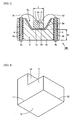
- FIG. 1 there is a cross-section representing an example of a semiconductor device according to Implementation mode 1 of the present invention.
- Figure 2 is a perspective view showing one mode of the semiconductor element represented in Figure 1.
- a semiconductor device 100 of Figure 1 there is a semiconductor element 1 having a main surface 1a.
- a substrate 2 which is integrated with a frame part 2c on which the element is mounted.
- Substrate 2 has an upper surface 2a and a lower surface 2b.
- Main surface 1a of semiconductor element 1 is opposite upper surface 2a of substrate 2.
- main surface 1a is a rectangle.
- the length of the long side of main surface 1a is a length L, corresponds to that of long side 11.
- the length in the short side direction corresponds to that of short side 12. This is the same for other implementation modes, but if main surface 1a is rectangular, normally, the surface of the other side is approximately the same shape. However, this does not always have to be the case. As shown in Figure 3, there are examples of the main surface being other than a rectangle.
- the length in the long direction of the main surface of the semiconductor element of the present invention is measured from the outline of an image projected in a direction perpendicular to the main surface. Examples are shown in Figures 3A through 3E.
- the part displayed as L is the length in the long direction. For example, if it is a circle or square, length L is the diameter or the length of one of its sides, respectively.
- ratio L/H is 0.3 or greater.
- ratio L/H is 0.45 to 1.5, and more preferably it is between 0.5 and 1.25.
- Figure 4 is a cross-sectional diagram of a semiconductor device for schematically describing the release of heat.
- a heat Q is generated from semiconductor light emitting element 1, as shown by arrows 50, the heat spreads within substrate 2 and is transmitted to bottom surface 2b of substrate 2.
- distance Z By making distance Z larger, the area contributing to the heat release of bottom surface 2b of substrate 2 is enlarged. In other words, the heat generated from semiconductor light emitting element 1 is efficiently released.
- distance H must be increased.
- distance H is increased, and the amount of heat release from bottom surface 2b is increased.
- distance Y is preferably 2 times or greater the length L of first side 11.
- substrate 2 is a heat releasing member.
- the material will depend on the package design according to the needs of the semiconductor device. In addition to packaging the semiconductor device, there is also the need for ease of manufacturing, light weight, and a long usage lifespan. However, as described previously, the most important properties are that the heat expansion factor be similar to that of the semiconductor element and that it has a high heat conductivity.
- the heat conductivity of the substrate of the present invention is 170 W/m-K or greater, and preferably 200 W/m-K or greater.
- the material of the substrate is (1) various inorganic and organic materials and their compounds, (2) composite material in which these various inorganic and organic materials are microscopically mixed without being chemically combined. (3) combined material in which these materials are macroscopically combined.
- examples include: semi-metals such as carbon (for example, graphite, diamond), Si, and the like; metal materials having as the main components Al, Cu, Ag, Au, and transition metals of Groups 4a through 7a, 8a of the periodic table; compounds of semi-metals and metals such as TiC, ZrN, and the like; compounds of semi-metals such as SiC, B 4 C, and the like; compounds of semi-metals and non-metals such as Si 3 N 4 and BN and the like; and compounds of metals and semi-metals such as AlN.
- the organic materials these are compounds present in living organisms, in the natural world, and those which are synthesized. Examples include DNA, enzymes, natural or synthetic rubber, fibers, resin, organic metal compounds, and the like.
- the various materials of (1) are microscopically mixed and dispersed or arranged.
- various composite materials such as Cu-W, Cu-Mo, Al-SiC, Al-AlN, Ag-C, Si-SiC, and the like.
- some of the materials from (1) and (2) are combined in bulk. This can take many forms. Examples include: layered bodies of Cu and Mo, Al and SiC, and the like; board-shaped examples with the middle part being Cu and the outer perimeter being Cu-Mo; functionally layered examples in which there is a gradient with the amount of Cu changing in the thickness direction of a Cu-Mo layer, and the like. These are created as appropriate depending on the package design. We will introduce implementation examples of representative substrates below.
- the coefficient of thermal expansion is normally 5 to 12 x 10 -6 /K.
- the coefficient of thermal expansion is in the range of 8 to 20x10 -6 /K.
- the Cu content is preferably in the range of 5 to 40% by mass, more preferably in the range of 10 to 35% by mass, and even more preferably in the range of 10 to 20% by mass.
- a molded body with a main component of W or Mo powder is made, or this is further sintered, and a porous body is created. Cu is infiltrated into the pores (infiltrating method).
- a mixture of powder with main components of Cu and W or Cu and Mo is molded, and this is sintered (sintering method).
- the Al content is preferably in the range of 25 to 35 % by mass.
- This material is manufactured by the following methods: a casting method in which SiC powder is dispersed in Al molten solution and cooled; an infiltration method in which Al is infiltrated into the pores of a porous body having a main component of SiC; a sintering method in which after molding a mixture having main components of Al powder and SiC powder, this is sintered.
- connection means such as a bonding wire, flip chip, via hole, and the like, is provided between substrate 2 and semiconductor element 1.
- a metal layer 13 is formed on element mounting surface 2a of substrate 2 for connection with the semiconductor element or for electrifying the element.
- the surface roughness of surface 2a preferably has a maximum roughness by JIS standards (JIS B 0601) of Rmax in a range of 0.1 to 20 micrometers. When the maximum roughness is less than 0.1 micrometers, an anchoring effect is difficult to achieve when forming the metal layer.
- Rmax exceeds 20 micrometers
- the amount of adsorbed gas such as oxygen and the like on surface 2a increases, and the amount of gas released when forming the metal layer increases, and the degree of vacuum needed for film formation is difficult to achieve.
- Rmax is between 0.1 micrometers and 8 micrometers. When Rmax exceeds 8 micrometers, holes are easily generated during joining, and there can be unevenness in joining strength.
- the semiconductor device of the present invention by having the dimensions of the substrate and the main surface of the semiconductor element within a prescribed range as described above, the heat generated by the element is released smoothly. With this, the effects of excess temperature rise by the element, such as reduction in output of the semiconductor device or the deterioration of members near the element, is reduced greatly. Increased output from the device and extended usage life is possible.
- FIG. 5 there is shown a cross-section of a semi-conductor device according to Implementation mode 2 of the present invention.
- semiconductor element 1 is a light emitting element.
- the design of device 100 is controlled as described above with regard to H/L.
- Metal layer 13 is formed on element mounting surface 2a and is preferably formed with the surface form as described above. With this implementation mode, the metal layer has a role of reflecting light emitted by light emitting element 1.
- the metal layer is normally constructed from a metal with a high reflectance such as silver or aluminum or from a metal having a main component of a high reflectance metal.
- Metal layer 13 is formed by plating or vapor deposition so that it covers the element mounting surface.
- the metal layer may be formed on other parts, not just the element mounting surface, or it may be formed on the entire surface of substrate 2.
- the substrate body is conductive, for example if it is of a metal material or the like, bright silver plating by an electroplating method is preferred.
- the reflectance of the element mounting surface itself is high, there does not have to be a metal layer.
- metal layer 13 is provided in a cavity 2u, but it is also possible to use a substrate 2 without cavity 2u and have metal layer 13 provided on element mounting surface 2a of substrate 2.
- the thickness of substrate 2, or in other words the distance H from bottom surface 2b to element mounting surface 2a, can be established according to the dimensions of semiconductor light emitting element 1.
- distance H can be 0.3 mm or greater and 10 mm or less.
- Semiconductor light emitting element 1 is provided so that it contacts metal layer 13.
- the element is constructed from a compound semiconductor light emitting element of the II-VI group or III-V group, such as ZnSe, GaAs, GaP, GaN, InP, and the like.
- group II elements include zinc (Zn) and cadmium (Cd).
- Group III elements include boron (B), aluminum (Al), gallium (Ga), and indium (In).
- Group V elements include nitrogen (N), phosphorus (P), arsenic (As), and antimony (Sb).
- Group VI elements include oxygen (O), sulfur (S), selenium (Se), and tellurium (T). These compound semiconductors can be formed on top of a substrate of sapphire or the like.
- Substrate 2 can be constructed from a Fe-Ni alloy or Fe-Ni-Co alloy, for example.
- an intermediate layer (not shown) provided between element mounting surface 2a and metal layer 13.
- examples include Ni, Ni-Cr, Ni-P, Ni-B, Ni-Co, Cu, and Au, and the like. These are formed by plating.
- examples include Ti, V, Cr, Ni, NiCr alloy, Cu, W, Zr, Nb, and Ta, and the like.
- the intermediate layer can be multi-layered with a plating layer and/or vapor deposition layer described above. The thickness of the intermediate layer is preferably 0.01 to 5 micrometers, and more preferably 0.1 micrometers to 1 micrometer.
- FIG. 6 shows a perspective view of the semiconductor element of this implementation mode.
- the element has a step part 1d, but this can be eliminated.
- Side 11 is the long side of semiconductor light emitting element 1
- side 12 is the short side.
- the length of side 11 corresponds to length L. and extends approximately perpendicular to step part 1d of light emitting element.
- Side 12 extends approximately parallel to the step part.
- main surface 1a is not rectangular, it is as described previously. For example, even if main surface 1a is rectangular but with rounded corners, an extrapolation line is drawn along the outline projection of main surface 1a, and this is determined to be long side L.
- semiconductor light emitting element 1 power is supplied from main surface 1a and/or from the side opposite of main surface 1a.
- Light is emitted from a light emitting layer (not shown) provided within semiconductor light emitting element.
- Semiconductor light emitting element can be a light emitting diode, or it can be a semiconductor laser.
- the wavelength of the light generated by semiconductor light emitting element is not particularly limited.
- holes 2h which pass through substrate 2. Holes 2h are approximately cylindrical in shape. On the inside of holes 2h, there are an insulating glass 4 and pins 3a and 3b. Pins 3a and 3B supply power to semiconductor light emitting element 1 and are constructed from stainless steel (SUS) or a Fe-Co-Ni alloy. In addition, as long as the electrical resistance is small, pins 3a and 3b can be formed from other compositions. Insulating glass 4 is provided for positioning of pins 3a and 3b inside holes 2h. Insulating glass 4 fills holes 2h and also has the function of insulating pins 3a and 3b and substrate 2.
- Bonding wires 21 and 22 electrically connect pins 3a and 3b with semiconductor light emitting element 1. The power supplied from pins 3a and 3b is supplied to semiconductor light emitting element 1 via bonding wires 21 and 22. Bonding wires 21 and 22 can be constructed from gold, aluminum, or their alloys.
- the length in the long direction in other words, the length L of the long side is preferably 1 mm or greater, or the surface area of main surface 1a is preferably 1 mm 2 or greater.
- the heat generated from semiconductor light emitting element 1 is not adequately released to the exterior and removed, the temperature of the element itself rises. This could result in reduced light emitting efficiency, and it may lead to shifting of wavelengths of light so that light is no longer being emitted at a constant color. Furthermore, due to the heat, peripheral members such as fluorescent bodies and the like can deteriorate. As a result of the above, the lifespan of the semiconductor device is shortened. In particular, when length L of the light emitting element exceeds 1 mm, the temperature in the central part of the element tends to rise, and its lifespan is shortened. In the semiconductor device of the present implementation mode, because H/L is optimized, an adequate release of heat is conducted, and the above problems are kept in check.
- Figure 7 shows a cross-section of a semiconductor device according to Implementation mode 3 of the present invention.
- Figure 8 is a cross-section showing an enlargement of the area within circle V of Figure 7.
- the design of this semiconductor device is controlled as described above with regard to H/L.
- a metal layer is formed on the element mounting surface and is preferably formed with the surface form as described above. The metal layer has a role of reflecting light emitted by light emitting element 1.
- semiconductor device 100 of this implementation mode has no pins.
- a connection member 33 is provided on top of substrate 2.
- a terminal plate 34 which is formed from an insulating plate 31 and an electrode 32, is affixed to substrate 2 by connection member 33.
- Connection member 33 is a solder or an adhesive for example.
- a groove 2t is formed on substrate 2 in order to prevent connection member 33 from flowing into cavity 2u. If connection member 33 flows into cavity 2u, this results in surface unevenness in cavity 2u, and the light reflectance is reduced.
- Other means may be used as long as the same object is achieved. For example, there can be an area with bumps.
- Insulating plate 31 is constructed from ceramic, for example. However, instead of insulating plate 31, an insulating film, such as silicon nitride film or silicon oxide film can be provided.
- a conductive electrode 32 for electrical connection with bonding wires 21 and 24. This electrode is formed by printing, vacuum deposition, plating, and the like. Groove 2t can be formed by mechanical processing or sand blasting.
- groove 2t can be formed by partially removing the undercoat plating formed on the surface of substrate 2 or it can be provided in a region which is not plated.
- the width of the groove is preferably 50 micrometers or greater and 1 mm or less. More preferably, it is 100 micrometers or greater and 500 micrometers or less. If the width is too narrow, the connection member can easily get over the groove. If the width is too large, it becomes wasted space.
- Implementation mode 3 of the present invention has a connection member 33 which is provided at a separate position from cavity 2u and which connects substrate 2 with terminal plate 34.
- Substrate 2 is provided with a groove 2t as a means for preventing connection member 33 from flowing into cavity 2u. With this construction, the semiconductor device of Implementation mode 3 of the present invention prevents reduction in light emitting efficiency of the device by preventing the connection member from covering the metal layer in the cavity.
- a semiconductor device 100 having a construction as shown in Figure 7 was prepared.
- the substrate was constructed from a composite material containing copper at 15% by mass and tungsten at 85% by mass, and the semiconductor light emitting element 1 was a GaN series compound semiconductor light emitting diode.
- Bottom surface 2b of semiconductor device 100 was mounted on top of a copper frame. Using materials described above, and having various measurements for dimension Y of substrate 2, dimension L (length L of the long side) of the element, and substrate thickness H (distance H from element mounting surface 2a to bottom surface 2b), the samples shown in Table 1 were prepared.
- the semiconductor light emitting elements 1 from Samples 1 through 10 were illuminated with a current of 1A. After one minute of illumination, temperatures T1 were measured by using a radiation thermometer (noncontact). Illumination was continued, and after three minutes of illumination, measurements for temperature T3 were taken for each of Samples 1 through 9. The rate of temperature increase ((T3-T1)/T1) were measured for each of Samples 1 through 10. These results are also shown in Table 1. With regard to the rate of temperature increase shown in Table 1, the double circle indicates that the rate of temperature increase was less than 10%. A single circle indicates that the rate of temperature increase was less than 20%. An X indicates that the rate of temperature increase was 20% or greater. As seen from Table 1, Sample 2, which is outside the scope of the present invention, had a large rate of temperature increase.
- samples with the substrate construction of Figure 1 were prepared.
- the substrates were approximately the same size as the above substrates and were made of composite material containing Al at 30% by mass and SiC at 70% by mass.
- Si semiconductor elements of approximately the same size as the light emitting element described above were used.
- the samples were in the approximately the same range of H/L as above. By following approximately the same steps and in the approximately same H/L range as described above, when the rate of temperature increase was confirmed, results with the same trends as described above were obtained.
- a semiconductor device that can adequately remove heat generated by the semiconductor element is provided.
- the semiconductor device equipped with a light emitting element a semiconductor device with excellent light emitting efficiency is provided.
Landscapes
- Led Device Packages (AREA)
- Led Devices (AREA)
Abstract
Description
| Sample No. | Substrate dimension Y (mm) | Element dimension L (mm) | Substrate thickness H (mm) | H/L | Rate of |
| 1 | 3 | 1 | 1 | 1 | o ○ |
| 2 | 3 | 1 | 0.2 | 0.2 | X |
| 3 | 3 | 1 | 0.3 | 0.3 | ○ |
| 4 | 3 | 1 | 0.45 | 0.45 | ○ |
| 5 | 3 | 1 | 0.5 | 0.5 | o ○ |
| 6 | 3 | 1 | 0.75 | 0.75 | o ○ |
| 7 | 3 | 1 | 1.25 | 1.25 | o ○ |
| 8 | 3 | 1 | 1.5 | 1.5 | o ○ |
| 9 | 3 | 1 | 2 | 2 | o ○ |
| 10 | 2 | 1 | 1 | 1 | o ○ |
Claims (3)
- A semiconductor device, comprising:a semiconductor element;a substrate having an upper surface on which said element is mounted and a bottom surface which is positioned on the opposite side;a ratio H/L being 0.3 or greater, with L being the length in the long direction of a main surface of said semiconductor element, and H being the distance from a semiconductor element mounting part on said upper surface of said substrate to said bottom surface.
- A semiconductor device as described in Claim 1, wherein:said semiconductor element is a light emitting element;a part of said substrate on which said element is mounted is formed as a cavity;and a metal layer is formed on said upper surface.
- A semiconductor device as described in Claim 2, wherein:there is a connection member which connects between said substrate and a terminal plate which supplies power to said semiconductor light emitting element;said connection member is placed at a position separate from said cavity;a means for preventing infiltration of said connection member into said cavity is provided on said upper surface adjacent to said connection member.
Applications Claiming Priority (3)
| Application Number | Priority Date | Filing Date | Title |
|---|---|---|---|
| JP2003069711 | 2003-03-14 | ||
| JP2003069711 | 2003-03-14 | ||
| PCT/JP2004/002982 WO2004082034A1 (en) | 2003-03-14 | 2004-03-08 | Semiconductor device |
Publications (2)
| Publication Number | Publication Date |
|---|---|
| EP1605523A1 true EP1605523A1 (en) | 2005-12-14 |
| EP1605523A4 EP1605523A4 (en) | 2012-04-04 |
Family
ID=32984625
Family Applications (1)
| Application Number | Title | Priority Date | Filing Date |
|---|---|---|---|
| EP20040718410 Withdrawn EP1605523A4 (en) | 2003-03-14 | 2004-03-08 | SEMICONDUCTOR DEVICE |
Country Status (6)
| Country | Link |
|---|---|
| US (3) | US7335925B2 (en) |
| EP (1) | EP1605523A4 (en) |
| JP (1) | JP4001169B2 (en) |
| KR (1) | KR101007164B1 (en) |
| CN (1) | CN100420048C (en) |
| WO (1) | WO2004082034A1 (en) |
Cited By (7)
| Publication number | Priority date | Publication date | Assignee | Title |
|---|---|---|---|---|
| EP1848042A1 (en) * | 2006-04-21 | 2007-10-24 | LEXEDIS Lighting GmbH | LED package with submount |
| EP1744374A4 (en) * | 2004-04-12 | 2009-05-20 | Sumitomo Electric Industries | SEMICONDUCTOR LIGHT EMITTING ELEMENT MOUNTING BRACKET, AND SEMICONDUCTOR LIGHT EMITTING ELECTROLUMINESCENT DEVICE USING THE SAME |
| WO2009132808A3 (en) * | 2008-04-30 | 2010-05-06 | Ledon Lighting Jennersdorf Gmbh | Led element with a thin-layer semiconductor element made of gallium nitride |
| US8044412B2 (en) | 2006-01-20 | 2011-10-25 | Taiwan Semiconductor Manufacturing Company, Ltd | Package for a light emitting element |
| EP2398081B1 (en) * | 2009-02-13 | 2018-05-09 | Denka Company Limited | Composite substrate for led light emitting element, method of production of same, and led light emitting element |
| EP2757604B1 (en) | 2011-09-13 | 2018-06-13 | Denka Company Limited | Method of manufacturing a clad material for led light-emitting element holding substrate |
| EP3357098B1 (en) * | 2015-11-03 | 2019-08-21 | ADE photonExa GmbH | Led illumination module |
Families Citing this family (36)
| Publication number | Priority date | Publication date | Assignee | Title |
|---|---|---|---|---|
| EP1605523A4 (en) * | 2003-03-14 | 2012-04-04 | Sumitomo Electric Industries | SEMICONDUCTOR DEVICE |
| JP4895777B2 (en) * | 2006-01-27 | 2012-03-14 | 京セラ株式会社 | WIRING BOARD FOR LIGHT EMITTING ELEMENT AND LIGHT EMITTING DEVICE |
| US20090273004A1 (en) * | 2006-07-24 | 2009-11-05 | Hung-Yi Lin | Chip package structure and method of making the same |
| JP2010512662A (en) | 2006-12-11 | 2010-04-22 | ザ リージェンツ オブ ザ ユニバーシティ オブ カリフォルニア | Transparent light emitting diode |
| JPWO2008111504A1 (en) * | 2007-03-12 | 2010-06-24 | 日亜化学工業株式会社 | High power light emitting device and package used therefor |
| KR101438826B1 (en) * | 2008-06-23 | 2014-09-05 | 엘지이노텍 주식회사 | Light emitting device |
| TWM354185U (en) * | 2008-09-25 | 2009-04-01 | Lighthouse Technology Co Ltd | Improved packaging substrate and light-emitting device applying the same |
| US7923739B2 (en) * | 2009-06-05 | 2011-04-12 | Cree, Inc. | Solid state lighting device |
| US8598602B2 (en) * | 2009-01-12 | 2013-12-03 | Cree, Inc. | Light emitting device packages with improved heat transfer |
| JP5245970B2 (en) * | 2009-03-26 | 2013-07-24 | 豊田合成株式会社 | LIGHT EMITTING DIODE, ITS MANUFACTURING METHOD, AND LAMP |
| KR101077479B1 (en) * | 2009-05-20 | 2011-10-27 | 주식회사 두성에이텍 | Method of manufacturing light emitting diode unit and light emitting diode unit manufactured by the method |
| US8686445B1 (en) | 2009-06-05 | 2014-04-01 | Cree, Inc. | Solid state lighting devices and methods |
| US9111778B2 (en) | 2009-06-05 | 2015-08-18 | Cree, Inc. | Light emitting diode (LED) devices, systems, and methods |
| US8860043B2 (en) * | 2009-06-05 | 2014-10-14 | Cree, Inc. | Light emitting device packages, systems and methods |
| JP5759376B2 (en) * | 2009-07-17 | 2015-08-05 | 電気化学工業株式会社 | Manufacturing method of LED chip assembly |
| US8890189B2 (en) | 2009-07-31 | 2014-11-18 | Denki Kagaku Kogyo Kabushiki Kaisha | Wafer for LED mounting, method for manufacturing same, and LED-mounted structure using the wafer |
| WO2011037876A1 (en) * | 2009-09-25 | 2011-03-31 | Cree, Inc. | Lighting device having heat dissipation element |
| US8502257B2 (en) * | 2009-11-05 | 2013-08-06 | Visera Technologies Company Limited | Light-emitting diode package |
| TW201126765A (en) * | 2010-01-29 | 2011-08-01 | Advanced Optoelectronic Tech | Package structure of compound semiconductor and manufacturing method thereof |
| CN102194964A (en) * | 2010-03-12 | 2011-09-21 | 展晶科技(深圳)有限公司 | Compound semi-conductor packaging structure and manufacturing method thereof |
| US8269244B2 (en) | 2010-06-28 | 2012-09-18 | Cree, Inc. | LED package with efficient, isolated thermal path |
| US8648359B2 (en) | 2010-06-28 | 2014-02-11 | Cree, Inc. | Light emitting devices and methods |
| USD643819S1 (en) | 2010-07-16 | 2011-08-23 | Cree, Inc. | Package for light emitting diode (LED) lighting |
| TWI414050B (en) * | 2010-10-19 | 2013-11-01 | 聯京光電股份有限公司 | Packaging board and manufacturing method thereof |
| US8610140B2 (en) | 2010-12-15 | 2013-12-17 | Cree, Inc. | Light emitting diode (LED) packages, systems, devices and related methods |
| USD679842S1 (en) | 2011-01-03 | 2013-04-09 | Cree, Inc. | High brightness LED package |
| TW201251140A (en) | 2011-01-31 | 2012-12-16 | Cree Inc | High brightness light emitting diode (LED) packages, systems and methods with improved resin filling and high adhesion |
| CN103348496A (en) | 2011-02-07 | 2013-10-09 | 克利公司 | Components and methods for light emitting diode (LED) lighting |
| US8598694B2 (en) * | 2011-11-22 | 2013-12-03 | Infineon Technologies Ag | Chip-package having a cavity and a manufacturing method thereof |
| JP5792694B2 (en) * | 2012-08-14 | 2015-10-14 | 株式会社東芝 | Semiconductor light emitting device |
| USD774006S1 (en) * | 2014-08-27 | 2016-12-13 | Mitsubishi Electric Corporation | Light source module |
| JP6801950B2 (en) * | 2015-04-15 | 2020-12-16 | ショット日本株式会社 | Through Silicon Via and Semiconductor Package |
| TWI598538B (en) * | 2015-07-31 | 2017-09-11 | 宏齊科技股份有限公司 | Portable light-emitting device without using pre-storage power supply and LED package structure thereof |
| JP7027129B2 (en) * | 2017-11-09 | 2022-03-01 | シチズン電子株式会社 | Light emitting device |
| US11592166B2 (en) | 2020-05-12 | 2023-02-28 | Feit Electric Company, Inc. | Light emitting device having improved illumination and manufacturing flexibility |
| US11876042B2 (en) | 2020-08-03 | 2024-01-16 | Feit Electric Company, Inc. | Omnidirectional flexible light emitting device |
Family Cites Families (30)
| Publication number | Priority date | Publication date | Assignee | Title |
|---|---|---|---|---|
| JPS5176971A (en) * | 1974-12-27 | 1976-07-03 | Hitachi Ltd | |
| JPS59228778A (en) * | 1983-06-09 | 1984-12-22 | Sumitomo Electric Ind Ltd | Light emitting diode |
| JPS6074485A (en) | 1983-09-29 | 1985-04-26 | Toshiba Corp | Semiconductor light-emitting device |
| US5529852A (en) * | 1987-01-26 | 1996-06-25 | Sumitomo Electric Industries, Ltd. | Aluminum nitride sintered body having a metallized coating layer on its surface |
| JPH0436473A (en) * | 1990-05-31 | 1992-02-06 | Daiichi Kosho Kk | Chemical plating liquid composition of lead or lead-tin alloy |
| EP0952617B1 (en) * | 1993-04-28 | 2004-07-28 | Nichia Corporation | Gallium nitride-based III-V group compound semiconductor device |
| US5925898A (en) * | 1996-07-18 | 1999-07-20 | Siemens Aktiengesellschaft | Optoelectronic transducer and production methods |
| JPH1051065A (en) * | 1996-08-02 | 1998-02-20 | Matsushita Electron Corp | Semiconductor laser device |
| JPH10150227A (en) * | 1996-11-15 | 1998-06-02 | Rohm Co Ltd | Chip type light emitting device |
| JP3432113B2 (en) * | 1997-07-07 | 2003-08-04 | シャープ株式会社 | Optical semiconductor device |
| JPH11163419A (en) * | 1997-11-26 | 1999-06-18 | Rohm Co Ltd | Light emitting device |
| DE19829197C2 (en) * | 1998-06-30 | 2002-06-20 | Siemens Ag | Component emitting and / or receiving radiation |
| US6335548B1 (en) * | 1999-03-15 | 2002-01-01 | Gentex Corporation | Semiconductor radiation emitter package |
| CA2380356C (en) * | 1999-07-26 | 2011-01-18 | Labosphere Institute | Bulk-shaped lens, light-emitting unit, lighting equipment and optical information system |
| US6252726B1 (en) * | 1999-09-02 | 2001-06-26 | Lightlogic, Inc. | Dual-enclosure optoelectronic packages |
| JP2001168443A (en) * | 1999-12-06 | 2001-06-22 | Kyocera Corp | Package for storing optical semiconductor elements |
| JP4897133B2 (en) | 1999-12-09 | 2012-03-14 | ソニー株式会社 | Semiconductor light emitting device, method for manufacturing the same, and mounting substrate |
| US6486499B1 (en) | 1999-12-22 | 2002-11-26 | Lumileds Lighting U.S., Llc | III-nitride light-emitting device with increased light generating capability |
| US6885035B2 (en) * | 1999-12-22 | 2005-04-26 | Lumileds Lighting U.S., Llc | Multi-chip semiconductor LED assembly |
| JP4432275B2 (en) * | 2000-07-13 | 2010-03-17 | パナソニック電工株式会社 | Light source device |
| JP4309030B2 (en) * | 2000-07-17 | 2009-08-05 | 三菱電線工業株式会社 | Light emitting device |
| WO2002045470A1 (en) * | 2000-11-30 | 2002-06-06 | Tokuyama Corporation | Substrate and production method therefor |
| JP4737842B2 (en) | 2001-01-30 | 2011-08-03 | 京セラ株式会社 | Manufacturing method of light emitting element storage package |
| US6874910B2 (en) * | 2001-04-12 | 2005-04-05 | Matsushita Electric Works, Ltd. | Light source device using LED, and method of producing same |
| JP4055373B2 (en) * | 2001-05-31 | 2008-03-05 | 日亜化学工業株式会社 | Method for manufacturing light emitting device |
| JP3956941B2 (en) * | 2001-06-15 | 2007-08-08 | 日亜化学工業株式会社 | Nitride semiconductor light emitting device and light emitting device using the same |
| JP4959071B2 (en) | 2001-07-04 | 2012-06-20 | ローム株式会社 | Surface mount semiconductor device |
| JP2003066287A (en) | 2001-08-24 | 2003-03-05 | Citizen Electronics Co Ltd | Bidirectional optical transmission device |
| US6531328B1 (en) * | 2001-10-11 | 2003-03-11 | Solidlite Corporation | Packaging of light-emitting diode |
| EP1605523A4 (en) * | 2003-03-14 | 2012-04-04 | Sumitomo Electric Industries | SEMICONDUCTOR DEVICE |
-
2004
- 2004-03-08 EP EP20040718410 patent/EP1605523A4/en not_active Withdrawn
- 2004-03-08 WO PCT/JP2004/002982 patent/WO2004082034A1/en not_active Ceased
- 2004-03-08 JP JP2005503515A patent/JP4001169B2/en not_active Expired - Fee Related
- 2004-03-08 US US10/539,926 patent/US7335925B2/en not_active Expired - Lifetime
- 2004-03-08 KR KR1020057013031A patent/KR101007164B1/en not_active Expired - Fee Related
- 2004-03-08 CN CNB2004800040997A patent/CN100420048C/en not_active Expired - Fee Related
-
2007
- 2007-10-30 US US11/929,492 patent/US7504671B2/en not_active Expired - Lifetime
- 2007-10-30 US US11/929,387 patent/US7420223B2/en not_active Expired - Lifetime
Cited By (13)
| Publication number | Priority date | Publication date | Assignee | Title |
|---|---|---|---|---|
| EP1744374A4 (en) * | 2004-04-12 | 2009-05-20 | Sumitomo Electric Industries | SEMICONDUCTOR LIGHT EMITTING ELEMENT MOUNTING BRACKET, AND SEMICONDUCTOR LIGHT EMITTING ELECTROLUMINESCENT DEVICE USING THE SAME |
| US7897990B2 (en) | 2004-04-12 | 2011-03-01 | Sumitomo Electric Industries, Ltd. | Semiconductor light emitting element mounting member, and semiconductor light emitting device employing it |
| US8044412B2 (en) | 2006-01-20 | 2011-10-25 | Taiwan Semiconductor Manufacturing Company, Ltd | Package for a light emitting element |
| US8552460B2 (en) | 2006-01-20 | 2013-10-08 | Tsmc Solid State Lighting Ltd. | Package for a light emitting element |
| EP2387082A3 (en) * | 2006-04-21 | 2014-08-06 | Tridonic Jennersdorf GmbH | LED platform having a LED chip on a membrane |
| WO2007121973A1 (en) * | 2006-04-21 | 2007-11-01 | Lexedis Lighting Gmbh | Led platform having a led chip on a membrane |
| EP1848042A1 (en) * | 2006-04-21 | 2007-10-24 | LEXEDIS Lighting GmbH | LED package with submount |
| US8946740B2 (en) | 2006-04-21 | 2015-02-03 | Lexedis Lighting Gmbh | LED platform with membrane |
| WO2009132808A3 (en) * | 2008-04-30 | 2010-05-06 | Ledon Lighting Jennersdorf Gmbh | Led element with a thin-layer semiconductor element made of gallium nitride |
| CN102047451B (en) * | 2008-04-30 | 2013-05-08 | 莱登照明詹纳斯多夫股份公司 | LED element with a thin-layer semiconductor element made of gallium nitride |
| EP2398081B1 (en) * | 2009-02-13 | 2018-05-09 | Denka Company Limited | Composite substrate for led light emitting element, method of production of same, and led light emitting element |
| EP2757604B1 (en) | 2011-09-13 | 2018-06-13 | Denka Company Limited | Method of manufacturing a clad material for led light-emitting element holding substrate |
| EP3357098B1 (en) * | 2015-11-03 | 2019-08-21 | ADE photonExa GmbH | Led illumination module |
Also Published As
| Publication number | Publication date |
|---|---|
| JP4001169B2 (en) | 2007-10-31 |
| CN100420048C (en) | 2008-09-17 |
| JPWO2004082034A1 (en) | 2006-06-15 |
| CN1748327A (en) | 2006-03-15 |
| US7420223B2 (en) | 2008-09-02 |
| US20080105894A1 (en) | 2008-05-08 |
| WO2004082034A1 (en) | 2004-09-23 |
| KR101007164B1 (en) | 2011-01-12 |
| US7335925B2 (en) | 2008-02-26 |
| US20060118808A1 (en) | 2006-06-08 |
| KR20050106399A (en) | 2005-11-09 |
| US7504671B2 (en) | 2009-03-17 |
| US20080067540A1 (en) | 2008-03-20 |
| EP1605523A4 (en) | 2012-04-04 |
Similar Documents
| Publication | Publication Date | Title |
|---|---|---|
| US7504671B2 (en) | Semiconductor device | |
| US9147812B2 (en) | Methods of assembly for a semiconductor light emitting device package | |
| KR101045507B1 (en) | Light emitting element mounting member and semiconductor device using same | |
| EP0183016B1 (en) | Material for a semiconductor device and process for its manufacture | |
| CN101097847B (en) | Nickel-tin bonding systems for semiconductor wafers and devices | |
| US8183588B2 (en) | High efficiency group III nitride LED with lenticular surface | |
| TWI406387B (en) | Light emitting diode (LED) element and manufacturing method thereof | |
| CN100438103C (en) | Mounting member for semiconductor light emitting element and semiconductor light emitting device using the same | |
| JP2007142479A (en) | Semiconductor device | |
| US20060154393A1 (en) | Systems and methods for removing operating heat from a light emitting diode | |
| KR100768539B1 (en) | Semiconductor Emission Emitter Package | |
| CN1529357A (en) | Package for accommodating semiconductor chips, manufacturing method thereof, and semiconductor device | |
| CN118281141A (en) | Light Emitting Diode Package | |
| WO2017223255A1 (en) | Light emitting diode package | |
| JP2007250979A (en) | Semiconductor package | |
| Horng et al. | Optimized thermal management from a chip to a heat sink for high-power GaN-based light-emitting diodes | |
| JP2004200347A (en) | Light emitting diode with high heat dissipation performance | |
| JP2008198962A (en) | Light emitting device and manufacturing method thereof | |
| US20250287767A1 (en) | Light source and substrate | |
| CN103392241A (en) | Optoelectronic semiconductor device and method for producing an optoelectronic semiconductor device |
Legal Events
| Date | Code | Title | Description |
|---|---|---|---|
| PUAI | Public reference made under article 153(3) epc to a published international application that has entered the european phase |
Free format text: ORIGINAL CODE: 0009012 |
|
| 17P | Request for examination filed |
Effective date: 20050628 |
|
| AK | Designated contracting states |
Kind code of ref document: A1 Designated state(s): AT BE BG CH CY CZ DE DK EE ES FI FR GB GR HU IE IT LI LU MC NL PL PT RO SE SI SK TR |
|
| AX | Request for extension of the european patent |
Extension state: AL LT LV MK |
|
| DAX | Request for extension of the european patent (deleted) | ||
| RBV | Designated contracting states (corrected) |
Designated state(s): DE FR GB |
|
| RIN1 | Information on inventor provided before grant (corrected) |
Inventor name: TSUZUKI, YASUSHI Inventor name: ISHII, TAKASHI Inventor name: HIGAKI, KENJIROITAMI WORKS OF SUMITOMO ELECTRIC IN Inventor name: ISHIDU, SADAMU |
|
| A4 | Supplementary search report drawn up and despatched |
Effective date: 20120306 |
|
| RIC1 | Information provided on ipc code assigned before grant |
Ipc: H01L 33/64 20100101AFI20120229BHEP |
|
| 17Q | First examination report despatched |
Effective date: 20120612 |
|
| GRAP | Despatch of communication of intention to grant a patent |
Free format text: ORIGINAL CODE: EPIDOSNIGR1 |
|
| RIC1 | Information provided on ipc code assigned before grant |
Ipc: H01L 33/64 20100101AFI20151105BHEP Ipc: H01L 33/62 20100101ALN20151105BHEP |
|
| INTG | Intention to grant announced |
Effective date: 20151123 |
|
| RIC1 | Information provided on ipc code assigned before grant |
Ipc: H01L 33/62 20100101ALN20151113BHEP Ipc: H01L 33/64 20100101AFI20151113BHEP |
|
| STAA | Information on the status of an ep patent application or granted ep patent |
Free format text: STATUS: THE APPLICATION IS DEEMED TO BE WITHDRAWN |
|
| 18D | Application deemed to be withdrawn |
Effective date: 20160405 |