EP1603330A2 - Verfahren und Vorrichtung zur Rekonstruktion und Regelung der Phasenlage eines Abtasttaktes bezüglich eines abzutastenden analogen Signals - Google Patents
Verfahren und Vorrichtung zur Rekonstruktion und Regelung der Phasenlage eines Abtasttaktes bezüglich eines abzutastenden analogen Signals Download PDFInfo
- Publication number
- EP1603330A2 EP1603330A2 EP05011782A EP05011782A EP1603330A2 EP 1603330 A2 EP1603330 A2 EP 1603330A2 EP 05011782 A EP05011782 A EP 05011782A EP 05011782 A EP05011782 A EP 05011782A EP 1603330 A2 EP1603330 A2 EP 1603330A2
- Authority
- EP
- European Patent Office
- Prior art keywords
- analog signal
- sampling
- phase position
- signal
- sampled
- Prior art date
- Legal status (The legal status is an assumption and is not a legal conclusion. Google has not performed a legal analysis and makes no representation as to the accuracy of the status listed.)
- Granted
Links
- 238000000034 method Methods 0.000 title claims abstract description 24
- 230000001105 regulatory effect Effects 0.000 title claims description 4
- 238000005070 sampling Methods 0.000 claims abstract description 115
- 230000002123 temporal effect Effects 0.000 claims abstract description 46
- 230000009466 transformation Effects 0.000 claims description 6
- 230000004069 differentiation Effects 0.000 claims description 4
- 230000001276 controlling effect Effects 0.000 claims description 3
- 238000004364 calculation method Methods 0.000 description 9
- 230000006870 function Effects 0.000 description 6
- 239000011159 matrix material Substances 0.000 description 6
- 238000011156 evaluation Methods 0.000 description 4
- 230000002349 favourable effect Effects 0.000 description 4
- 230000008569 process Effects 0.000 description 4
- 238000000926 separation method Methods 0.000 description 4
- 238000011161 development Methods 0.000 description 3
- 230000018109 developmental process Effects 0.000 description 3
- 230000001419 dependent effect Effects 0.000 description 2
- 238000009795 derivation Methods 0.000 description 2
- 230000006399 behavior Effects 0.000 description 1
- 230000008859 change Effects 0.000 description 1
- 238000006243 chemical reaction Methods 0.000 description 1
- 238000012937 correction Methods 0.000 description 1
- 230000008878 coupling Effects 0.000 description 1
- 238000010168 coupling process Methods 0.000 description 1
- 238000005859 coupling reaction Methods 0.000 description 1
- 230000006866 deterioration Effects 0.000 description 1
- 238000010586 diagram Methods 0.000 description 1
- 125000000524 functional group Chemical group 0.000 description 1
- 230000010354 integration Effects 0.000 description 1
- 238000007620 mathematical function Methods 0.000 description 1
- 230000000737 periodic effect Effects 0.000 description 1
- 238000012545 processing Methods 0.000 description 1
- 230000003068 static effect Effects 0.000 description 1
- 230000001360 synchronised effect Effects 0.000 description 1
- 238000012549 training Methods 0.000 description 1
Images




Classifications
-
- H—ELECTRICITY
- H03—ELECTRONIC CIRCUITRY
- H03M—CODING; DECODING; CODE CONVERSION IN GENERAL
- H03M1/00—Analogue/digital conversion; Digital/analogue conversion
- H03M1/12—Analogue/digital converters
- H03M1/124—Sampling or signal conditioning arrangements specially adapted for A/D converters
- H03M1/1245—Details of sampling arrangements or methods
- H03M1/1255—Synchronisation of the sampling frequency or phase to the input frequency or phase
-
- G—PHYSICS
- G09—EDUCATION; CRYPTOGRAPHY; DISPLAY; ADVERTISING; SEALS
- G09G—ARRANGEMENTS OR CIRCUITS FOR CONTROL OF INDICATING DEVICES USING STATIC MEANS TO PRESENT VARIABLE INFORMATION
- G09G5/00—Control arrangements or circuits for visual indicators common to cathode-ray tube indicators and other visual indicators
- G09G5/003—Details of a display terminal, the details relating to the control arrangement of the display terminal and to the interfaces thereto
- G09G5/006—Details of the interface to the display terminal
- G09G5/008—Clock recovery
Definitions
- the invention relates to a method and a device, with which the phase position of a sampling clock with respect to a analog signal to be sampled reconstructed and can be regulated.
- analog video signals In the processing or evaluation of analog signals, especially analog video signals, these are often coupled sampled. In the case of analog video signals occurs in particular often a line-coupled scan. This means that analog signal exactly at the sampling frequency (also called pixel frequency designated) to be displayed on a screen or monitor Pixels are sampled, with each individual pixel once sampled or sampled.
- sampling frequency also called pixel frequency designated
- coupled sampling of analog signals is not just the sampling or pixel frequency of importance, but also the phase position of the sampling clock with respect to the scanned Signal, for example, a pixel signal.
- the phase angle is kept constant.
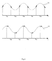
- the illustrated herein Course of an analog signal 10 carries the information itself alternating signal values W1 and W2.
- the signal value W1 could be a black pixel be assigned to the signal value W2, however, a white pixel.
- the analog signal 10 is at a time interval of Ta, which the inverse sampling frequency represents different Sampling times 12 sampled, which represented by dots Samples 14 are obtained.
- the lower graph in Figure 1 illustrates the facts at optimal phase angle of the sampling clock with respect to the analog signal 10.
- the samples 14 differ by the maximum possible separation of the sampling results D, so that Sampling results E1, which clearly the signal value W1 are assignable, and sampling results E2, which is beyond doubt belong to the signal value W2. Accordingly, the phase position the sampling clock with respect to the analog signal and thus the mentioned synchronization of considerable importance for the Evaluability of the signal.
- the amount of phase deviation of the signal from the sample clock or, if present, not known by a synchronizing pulse because of the coupled sampling only one sampling point per signal to be sampled, especially in the line-coupled Sampling of an analog video signal only one sample per pixel, is available.
- the invention is thus based on the problem of a method to provide with which the phase position of the sampling clock with respect to the analog signal to be sampled and reliably determined and regulated.
- the invention is based on the problem of a device to provide with which such Method is practically feasible.
- the idea underlying the invention is in addition to the usual sampling or sample values in addition to different Times temporal gradient of the analog signal to determine or to sample from the specific sample values and the determined temporal gradient the original to reconstruct analog signals at least in sections, with the help of the reconstructed waveform the phase angle of the sampling clock relative to the analog signal determine and supply them to a control loop, which the Adjusted phase position in a suitable manner.
- phase position of the sampling clock with respect to the analog signal determinable with sufficient accuracy and in a control loop includable.
- a phasing can not only in static pictures, but also in moving pictures be performed. Since a possible phase jump immediately can be corrected, for example within a row with video signals, the evaluation or the picture remains sharp and high contrast and a phase jump would be from an observer, for example, on a monitor, usually not be noticed.
- the analog signal 10 as shown in Figure 2 with the sampling clock Ta which the represents inverse sampling frequency sampled equidistant.
- a however, continuous sampling at this frequency is not absolutely necessary.
- Figure 2 illustrates the influence of the phase position on the temporal Gradients in the sampling points. While at the upper graphs shown unfavorable phase position the gradients assume maximum values in the sampling times in the case of the ideal phase position shown in the lower graph the sampling times always a disappearing temporal Gradient before. This fact can be used to determine the phase position the sampling clock with respect to the analog signal to be sampled 10 are used. For this, however, are knowledge about at least part of the time course of the analogue Signal 10 required.
- the reconstruction of the waveform is based on it, one for the analog waveform 10 suitable mathematical function to choose and their parameters by fitting this function to at least a portion of the samples and the temporal To determine gradients.
- This can be a variety of functions Find use, for example trigonometric Functions or polynomial functions.
- the approximate Reconstructions of the waveform 10 always a polynomial fourth Based on order.
- the Determination of the five coefficients of the fourth-order polynomial has always been the method of least squares used.
- Algorithms usable especially if not polynomial functions, but other functions or functional groups the reconstruction of the analog waveform 10 is based be placed.
- FIG. 3 shows the result of the reconstruction of the Waveform 10 at worst-case phase, Figure 4, however at most favorable phase position of the sampling clock. How to do that Takes representations, gives the respective approximately reconstructed Waveform 20 in both cases the waveform the analog signal 10 sufficiently accurate again.
- Exemplary for non-sinusoidal waveforms of the analogue Signals are in the figures 5 and 6 respectively subregions of a analog signal 10, which in turn based on the Samples 14a, 14b, 14c as well as in these sampling times present temporal gradient based on a polynomial fourth order were reconstructed.
- the approximately reconstructed Waveform 20 is dashed in both figures shown.
- the sampling was at worst Phase position, in Figure 6, however, almost ideal Phase position of the sampling clock.
- FIG. 5 here are the local 10 analog and analog extremes of the approximately reconstructed waveform 20 not more exactly together.
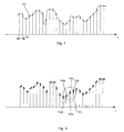
- FIG. 7 again shows a partial area a waveform of an analog signal 10, which is sampled with the sampling clock Ta.
- a 108 MHz data signal sampled at a sampling frequency of 108 MHz, which is a sample clock Ta and thus a period duration of 9.25 ns per sample.
- the temporal gradients are again determined at the sampling times, so that is shown in Figure 8 discretization of the waveform of the analog signal 10, wherein for the determination the phase angle of the sampling clock with respect to the analog Signal 10 only the marked area with the sampling times 12a, 12b, 12c and the samples 14a, 14b, 14c is used, which shown enlarged in Figure 9 is.
- the time axis is preferably no longer interpreted as such, but as the axis of the phase position.
- the control loop or the Control loop for controlling the phase position a base clock of 648 MHz
- per sampling clock Ta six phase positions can be adjusted.
- correspond two sampling clocks Ta in which in the present embodiment three samples 14a, 14b, 14c are scanned, twelve phase positions, as shown in Figure 9 on the phase angle axis are worn off.
- the timeline can continue as such are considered and at a later date the Conversion of a time information into a phase angle information respectively.
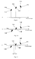
- a first Transformation of the samples carried out are the sampled values of the analog signal 10 into a desired one Value range transferred. This allows a simpler and more accurate calculation of the approximately reconstructed Signal waveform and the phase position.
- this transformation is done by addition the negative value of the median value of the samples, in FIG 9 so the negative sample 14b, to all samples 14a, 14b, 14c, which are used for the reconstruction of the waveform used portion of the analog signal 10th are located.
- three new samples 14A are obtained.
- 14B, 14C wherein the average sample 14B in FIG the phase lag axis comes to rest.
- the closest to a sample or time point Zero of the first time derivative of the reconstructed Signal waveform to determine and then their distance on the To determine the phase angle axis from said sampling time, which the sought phase difference ⁇ the phase position represents the sampling clock of the ideal phase position. is not a reinterpretation of the time axis as described above takes place in a phasing axis, so would be at this point the time interval of the determined, a sample or sampling time nearest zero from this sampling time to be determined and this in the phase difference ⁇ to convert the phase position of the sample clock from the ideal phase position.
- the mean sample 14B nearest zero of the first temporal Derivation of the waveform of the analog signal 10 is determined. This is advantageous because in the case of viewing the sample 14A or 14C is the nearest zero the time derivation outside of the considered value range could lie, leading to phase changes in the scheme could cause the phase angle and this possibly unstable would let.
- the nearest Zero point of such a sample can be determined, which is temporally between two further sampling times, the in turn part of the approximate reconstruction of the Waveform of the analog signal 10 used portion of the analog signal 10.
- Sample time 12b nearest zero of the first temporal derivative of the waveform of the analog signal 10 will preferably be the per se known Newton-Horner scheme used, with the starting value for the zero-search preferred the sampling time 12b of the sample under consideration 14B is used.
- the Newton-Horner scheme has the property that it is at the zero closest to the seed converges.
- the following is the time interval determined from the Zero of the selected sample 14B or the associated one Sampling point 12b, the phase angle of the sampling clock with respect to of the analog signal or the phase difference of the sampling clock determined to the ideal phase position and a control loop or fed to a control loop, which the phase position such Regulates that the sampling time 12b with the temporal Location of the particular zero coincides as possible.
- the control loop causes a setting of that phase position, which is the ideal Phasing comes closest.
- FIG. 12 shows a device according to the invention for reconstruction and controlling the phase angle of a sampling clock with respect to an analog signal to be sampled.
- an analog signal input designates, from which the analog Signal 10 to a to a first AD converter 40, for others to a temporal differentiation unit 50 introduced is.
- the device further comprises a clock 32, which provides a clock signal which, if necessary, modified by a phase locked loop, the first AD converter 40, a second AD converter 45 and a module for determining the Phase position 60 can be fed.
- the analog signal 10 is based of the clock signal 33 can be scanned at different times.
- the resulting samples 42 of the analog signal 10 are the module for determining the phase angle 60 can be fed.
- the time-differentiated analog signal 52 together with the clock signal 33 the second AD converter 45 are supplied. Due to the coupling with the clock signal 33, this second AD converter 45, the time-differentiated analog signal 52 at the same times.
- the first AD converter 40 it samples the analog signal 10, so sampled to each at some point Value of the analog signal 10 belonging to that time Value of the time differentiated signal 52 sampled can be.
- the second AD converter 45 After sampling the time-differentiated analog signal 52, the second AD converter 45 provides the module for determination the phase angle 60, the temporal gradient of the analog signal 54 at the sampling times available.
- the module for Determination of the phase position 60 itself which with reference to FIG. 13 will be explained in more detail, is the phase position or the phase difference with respect to the ideal phase of the sampling clock of the waveform of the analog signal 10 determinable.
- the calculated phase position or phase difference with respect to Ideal phase 82 is in the present embodiment a Proportional-integral controller (PI controller) fed to which Moreover, the clock signal 33 is applied.
- PI controller Proportional-integral controller
- the phase information 92 calculable for the control loop or the control loop which here as a delay locked loop (delay locked loop - DLL) 95 is executed.
- the mentioned PI controller provides an advantageous embodiment of the invention, since he is the System behavior in phase noise and phase jumps improved, however, it is not mandatory.
- control loop or the DLL 95 is based on the phase information 92 the clock of the clock 32 so changeable that this one outputs a shifted clock 97, which in turn be supplied as a new clock signal 33 to the other components which allows an iterative control of the phase position of the sampling clock with respect to the analog signal 10 to be scanned is.
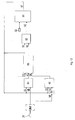
- FIG. 13 shows an exemplary embodiment of the module for determining the phase position 60 shown in FIG 12.
- a portion of the signal sampled by the analog 42 Signal 10 and by the temporal gradient of the analogue Signal 54 predetermined range of the waveform of the analog signal 10 for the approximate reconstruction of the Waveform are used, wherein at least a part the sampled values 42 of the analog signal 10 and at least a part of the temporal gradient of the analog signal 54 use find.
- the storage registers 62, 63, 64 are in the illustrated embodiment scanned at different times Samples of the analog signal 42 assignable. In the registers 65, 66, 67, however, can at different times certain temporal gradient of the analog signal 54 are stored. Below are the contents of the register 62, 63, 64, 65, 66, 67 can be fed to a microcontroller, in which the sectionwise reconstruction of the waveform of the analog signal 10 can take place.
- the phase angle of the sampling clock with respect to the analog signal 10 from the temporal Distance of this sampling time from the temporal position the particular zero, or when using a phase angle axis from the distance on the phase angle axis of the sampling time or values from the determined zero point determined become.
- the calculated phase position or phase difference compared to the ideal phase 82 of the sampling clock can ultimately from the module for determining the phase position 60 output become.
- An advantageous development of the invention further provides the Integration of a median operator 69, with the help of the in the registers 62, 63, 64 stored samples of the analog Signals 42 are related to the middle of these values which allows a transformation of the samples of the analog Signal 42 is effected in the vicinity of the zero value. This allows a more accurate calculation of the reconstructed Waveform.
- the device according to the invention it is not necessary, the device according to the invention to continuously supply data for the calculation of the phase angle. In usually it is sufficient if the microcontroller after completion In one calculation, the values for the next calculation are available be put. As a phase change in general is very slow and rare, exists beyond the ability to focus only on individual reconstruction processes the phase position and corresponding control processes to restrict, for example, a process in the Center of a line of a video signal. In these cases would be for the calculation comparatively much time available.
- the calculation of the phase position of the sampling clock with respect to the Waveform of the analog signal 10 can be to any Time to be performed. This is especially true interesting, if hardware or components are saved should.
Landscapes
- Engineering & Computer Science (AREA)
- Theoretical Computer Science (AREA)
- Physics & Mathematics (AREA)
- Computer Hardware Design (AREA)
- General Physics & Mathematics (AREA)
- Synchronisation In Digital Transmission Systems (AREA)
- Analogue/Digital Conversion (AREA)
- Stabilization Of Oscillater, Synchronisation, Frequency Synthesizers (AREA)
Abstract
Description
- Figur 1
- aus dem Stand der Technik bekannter und bereits behandelter Einfluss der Phasenlage des Abtasttaktes bezüglich des abzutastenden analogen Signals auf die Verwertbarkeit bzw. Güte der Abtastergebnisse,
- Figur 2
- Einfluss der Phasenlage auf die zeitlichen Gradienten des analogen Signals in den Abtastzeitpunkt,
- Figur 3
- sinusoidaler Abschnitt eines analogen Signals sowie polynominale Rekonstruktion dieses Abschnitts bei ungünstigster Phasenlage,
- Figur 4
- sinusoidaler Abschnitt eines analogen Signals sowie polynominale Rekonstruktion bei günstigster Phasenlage,
- Figur 5
- weiteres Beispiel eines Ausschnitts aus einem analogen Signal sowie dessen Rekonstruktion bei ungünstigster Phasenlage,
- Figur 6
- weiteres Beispiel eines Ausschnitts aus einem analogen Signal sowie dessen Rekonstruktion bei günstigerer Phasenlage,
- Figur 7
- größerer, nicht periodischer Ausschnitt aus einem abzutastenden analogen Signal,
- Figur 8
- Diskretisierung des Signalausschnitts aus Figur 7 anhand der Abtastwerte sowie der zu den Abtastzeitpunkten vorliegenden zeitlichen Gradienten,
- Figur 9
- vergrößerte Darstellung des in Figur 8 markierten Bereichs,
- Figur 10
- Transformation der Werte aus Figur 9 in einen für die Auswertung günstigen Wertebereich,
- Figur 11
- Differenz Δϕ der aktuellen Phasenlage zur idealen Phasenlage,
- Figur 12
- Blockschaltbild einer erfindungsgemäßen Vorrichtung zur Rekonstruktion und Regelung der Phasenlage eines Abtasttaktes bezüglich eines abzutastenden analogen Signals,
- Figur 13
- Detaildarstellung des Moduls zur Bestimmung der Phasenlage (60) aus Figur 12.
- 10
- analoger Signal
- 12
- Abtastzeitpunkt
- 12a
- Abtastzeitpunkt
- 12b
- Abtastzeitpunkt
- 12c
- Abtastzeitpunkt
- 14
- Abtastwert
- 14A
- Abtastwert
- 14B
- Abtastwert
- 14C
- Abtastwert
- 14a
- Abtastwert
- 14b
- Abtastwert
- 14c
- Abtastwert
- 16a
- zeitlicher Gradient
- 16b
- zeitlicher Gradient
- 16c
- zeitlicher Gradient
- 20
- näherungsweise rekonstruierter Signalverlauf
- 30
- Eingang analoges Signal
- 32
- Taktgeber
- 33
- Taktsignal
- 35
- optionaler Tiefpassfilter
- 40
- AD-Wandler 1
- 42
- Abtastwerte des analogen Signals
- 45
- AD-Wandler 2
- 50
- zeitliche Differenziereinheit
- 52
- zeitlich differenziertes analoges Signal
- 54
- zeitliche Gradienten des analogen Signals
- 60
- Modul zur Bestimmung der Phasenlage
- 62
- Register 1
- 63
- Register 2
- 64
- Register 3
- 65
- Register 4
- 66
- Register 5
- 67
- Register 6
- 69
- Medianoperator
- 80
- Microcontroller
- 82
- berechnete Phasenlage bzw. -differenz gegenüber Idealphase
- 90
- PI-Regler
- 92
- Phaseninformation für DLL
- 95
- DLL
- 97
- verschobener Takt
- Ta
- Abtasttakt
- W1
- Signalwert 1
- W2
- Signalwert 2
- E
- nicht zuordenbare Abtastergebnisse
- E1
- W1 zuordenbare Abtastergebnisse
- E2
- W2 zuordenbare Abtastergebnisse
- D
- Trennung der Abtastergebnisse
- Δϕ
- Phasendifferenz gegenüber Idealphase
Claims (16)
- Verfahren zur Rekonstruktion und Regelung der Phasenlage eines Abtasttaktes (Ta) bezüglich eines abzutastenden analogen Signals (10) bestehend aus1.1 dem Abtasten von Werten (42) des analogen Signals (10) mit dem Abtasttakt (Ta) zu verschiedenen Zeitpunkten,1.2 der Bestimmung der zeitlichen Gradienten (54) des analogen Signals zu verschiedenen Zeitpunkten,1.3 der näherungsweisen Rekonstruktion des Signalsverlaufs des analogen Signals (10) in wenigstens einem Teilbereich des durch die abgetasteten Werte (42) und die bestimmten Gradienten (54) vorgegebenen Bereichs unter Verwendung wenigstens eines Teils der abgetasteten Werte (14a, 14b, 14c) des analogen Signals (10) und eines Teils der bestimmten zeitlichen Gradienten (16a, 16b, 16c),1.4 der Bestimmung einer einem Abtastzeitpunkt (12b) nächstgelegenen Nullstelle der ersten zeitlichen Ableitung des rekonstruierten Signalverlaufs,1.5 der Ermittlung der Phasenlage (Δϕ) des Abtasttaktes (Ta) bezüglich des analogen Signals (10) aus dem zeitlichen Abstand dieses Abtastzeitpunktes (12b) von der zeitlichen Lage der bestimmten Nullstelle,1.6 der Zuführung der ermittelten Phasenlage (Δϕ) in eine Regelschleife (95, 90), welche die Phasenlage (Δϕ) derart nachregelt, dass dieser Abtastzeitpunkt (12b) mit der zeitlichen Lage der bestimmten Nullstelle möglichst zusammenfällt.
- Verfahren nach Anspruch 1,
dadurch gekennzeichnet, dass die Gradienten des analogen Signals (45) in denjenigen Zeitpunkten bestimmt werden, in denen die Werte des analogen Signals (42) abgetastet werden. - Verfahren nach einem der Ansprüche 1 bis 2,
dadurch gekennzeichnet, dass mindestens drei Werte (14a, 14b 14c) des analogen Signals (10) abgetastet und in mindestens drei Zeitpunkten (12a, 12b, 12c) die zeitlichen Gradienten (16a, 16b, 16c) des analogen Signals (10) bestimmt werden. - Verfahren nach Anspruch 2,
dadurch gekennzeichnet, dass zur näherungsweise Rekonstruktion des Signalverlaufs des analogen Signals (10) drei Datenpaare bestehend aus je einem Abtastwert (14a, 14b, 14c) und dem zugehörigen zeitlichen Gradienten (16a, 16b, 16c) zum Abtastzeitpunkt (12a, 12b, 12c) des jeweiligen Abtastwertes (14a, 14b, 14c) herangezogen werden. - Verfahren nach einem der Ansprüche 3 oder 4,
dadurch gekennzeichnet, dass derjenige Abtastzeitpunkt (12b), dessen nächstgelegene Nullstelle der ersten zeitlichen Ableitung des näherungsweise rekonstruierten Signalverlaufs bestimmt wird, zeitlich zwischen zwei weiteren Abtastzeitpunkten (12a, 12c) liegt. - Verfahren nach einem der Ansprüche 1 bis 5,
dadurch gekennzeichnet, dass zur näherungsweisen Rekonstruktion des Signalverlaufs des analogen Signals (10) ein Polynom, insbesondere ein Polynom vierter Ordnung verwendet wird. - Verfahren nach Anspruch 6,
dadurch gekennzeichnet, dass zur Bestimmung geeigneter Koeffizienten des Polynoms die Methode der kleinsten Fehlerquadrate angewandt wird. - Verfahren nach einem der Ansprüche 1 bis 7,
dadurch gekennzeichnet, dass der für die Rekonstruktion des Signalverlaufs des analogen Signals (10) herangezogene Wertebereich der abgetasteten Werte (14a, 14b, 14c) des analogen Signals (10) durch eine Transformation in einen gewünschten Wertebereich überführt wird, insbesondere durch Addition eines einheitlichen Wertes zu allen im herangezogenen Wertebereich liegenden Abtastwerten (14a, 14b, 14c). - Verfahren nach einem der Ansprüche 1 bis 8,
dadurch gekennzeichnet, dass für die Bestimmung der einem Abtastzeitpunkt (14B) nächstgelegenen Nullstelle das Newton-Horner-Schema eingesetzt wird. - Vorrichtung zur Rekonstruktion und Regelung der Phasenlage (82) eines Abtasttaktes (Ta) bezüglich eines abzutastenden analogen Signals (10) umfassend10.1 einen Taktgeber (32) zur Erzeugung eines den Abtasttakt (Ta) bildenden Taktsignals (33),10.2 mindestens einen mit dem Taktgeber (32) gekoppelten AD-Wandler (40) zum Abtasten von Werten (42) des analogen Signals (10) zu verschiedenen Zeitpunkten,10.3 eine Einrichtung zur einfachen zeitlichen Differentiation des analogen Signals (50),10.4 mindestens einen mit dem Taktgeber (32) gekoppelten AD-Wandler (45) zum Abtasten des zeitlich differenzierten analogen Signals (52) zu verschiedenen Zeitpunkten,10.5 ein Modul zur Bestimmung der Phasenlage (60) durch10.5.1 näherungsweise Rekonstruktion des Signalverlaufs des analogen Signals (10) in wenigstens einem Teilbereich des durch die abgetasteten Werte (42, 54) des analogen Signals (10) und des differenzierten analogen Signals (52) vorgegebenen Bereichs des analogen Signals (10) unter Verwendung wenigstens eines Teils der abgetasteten Werte des analogen Signals (42) und wenigstens eines Teils der abgetasteten Werte des zeitlich differenzierten analogen Signals (54),10.5.2 die Bestimmung einer einem Abtastzeitpunkt (12b) nächstgelegenen Nullstelle der ersten zeitlichen Ableitung des näherungsweisen rekonstruierten Signalverlaufs,10.5.3 die Ermittlung der Phasenlage (82) des Abtasttaktes (Ta) bezüglich des analogen Signals (10) aus dem zeitlichen Abstand dieses Abtastzeitpunktes (12b) von der zeitlichen Lage der bestimmten Nullstelle,10.6 einen Regelkreis (95, 90) zur Nachführung der Phasenlage (82) des Abtasttaktes (Ta) bezüglich des analogen Signals (10) anhand der im Modul zur Bestimmung der Phasenlage (60) bestimmten Phasenlage (82).
- Vorrichtung nach Anspruch 10,
dadurch gekennzeichnet, dass die AD-Wandler (40, 45) derart mit dem Taktgeber (32) gekoppelt sind, dass zu jedem zu einem gewissen Zeitpunkt abgetasteten Wert (42) des analogen Signals (10) der zu diesem Zeitpunkt gehörige Wert (54) des zeitlich differenzierten Signals (52) abtastbar ist. - Vorrichtung nach einem der Ansprüche 10 bis 11,
dadurch gekennzeichnet, dass für jeden zur näherungsweisen Rekonstruktion des Signalverlaufs des analogen Signals (10) verwendeten abgetasteten Wert (42) des analogen Signals (10) je ein Speicherregister (62, 63, 64) und für jeden zu dieser Rekonstruktion abgetasteten Wert (54) des zeitlich differenzierten analogen Signals (52) ebenfalls je ein Speicherregister (65, 66, 67) vorgesehen ist, insbesondere jeweils drei Speicherregister. - Vorrichtung nach einem der Ansprüche 10 bis 12,
dadurch gekennzeichnet, dass das Modul zur Bestimmung der Phasenlage (60) einen Medianoperator (69) umfasst. - Vorrichtung nach einem der Ansprüche 10 bis 13,
dadurch gekennzeichnet, dass das Modul zur Bestimmung der Phasenlage (60) einen Microcontroller (80) umfasst. - Vorrichtung nach einem der Ansprüche 10 bis 14,
dadurch gekennzeichnet, dass der Regelkreis zur Nachführung der Phasenlage (95, 90) einen Verzögerungsregelkreis (delay locked loop - DLL) (95) umfasst. - Vorrichtung nach einem der Ansprüche 10 bis 15,
dadurch gekennzeichnet, dass der Regelkreis zur Nachführung der Phasenlage (95, 90) ein Regelelement (90), insbesondere einen Proportional-Integral-Regler (PI-Regler) umfasst.
Applications Claiming Priority (2)
| Application Number | Priority Date | Filing Date | Title |
|---|---|---|---|
| DE102004027093A DE102004027093A1 (de) | 2004-06-02 | 2004-06-02 | Verfahren und Vorrichtung zur Rekonstruktion und Regelung der Phasenlage eines Abtasttaktes bezüglich eines abzutastenden analogen Signals |
| DE102004027093 | 2004-06-02 |
Publications (3)
| Publication Number | Publication Date |
|---|---|
| EP1603330A2 true EP1603330A2 (de) | 2005-12-07 |
| EP1603330A3 EP1603330A3 (de) | 2007-10-03 |
| EP1603330B1 EP1603330B1 (de) | 2010-12-22 |
Family
ID=34937119
Family Applications (1)
| Application Number | Title | Priority Date | Filing Date |
|---|---|---|---|
| EP05011782A Expired - Lifetime EP1603330B1 (de) | 2004-06-02 | 2005-06-01 | Verfahren und Vorrichtung zur Rekonstruktion und Regelung der Phasenlage eines Abtasttaktes bezüglich eines abzutastenden analogen Signals |
Country Status (3)
| Country | Link |
|---|---|
| US (1) | US7215273B2 (de) |
| EP (1) | EP1603330B1 (de) |
| DE (2) | DE102004027093A1 (de) |
Families Citing this family (6)
| Publication number | Priority date | Publication date | Assignee | Title |
|---|---|---|---|---|
| US7656335B2 (en) | 2005-06-02 | 2010-02-02 | Micronas Gmbh | Device for determining a measure for a signal change and a method of phase control |
| DE102005055543A1 (de) * | 2005-11-18 | 2007-05-31 | Micronas Gmbh | Verfahren zum Einstellen von Abtast-Zeitpunkten eines Abtasttakts in einem Bildsignal-Abtastsystem bzw. Schaltung zum Durchführen eines solchen Verfahrens |
| TWI355854B (en) * | 2007-12-21 | 2012-01-01 | Ite Tech Inc | Digital image converting apparatus and method with |
| US7728753B2 (en) * | 2008-10-13 | 2010-06-01 | National Semiconductor Corporation | Continuous synchronization for multiple ADCs |
| DE102012207535A1 (de) * | 2012-05-07 | 2013-11-07 | Siemens Aktiengesellschaft | Isolierband-Material, Verfahren zur Herstellung und Verwendung dazu |
| EP3559685A1 (de) | 2016-12-21 | 2019-10-30 | Vestas Wind Systems A/S | Bestimmung einer eigenschaft eines elektrischen signals einer windturbine |
Family Cites Families (6)
| Publication number | Priority date | Publication date | Assignee | Title |
|---|---|---|---|---|
| DE19751719A1 (de) | 1997-11-21 | 1999-05-27 | Thomson Brandt Gmbh | Signalverarbeitungsverfahren für ein analoges Bildsignal |
| US6473131B1 (en) * | 2000-06-30 | 2002-10-29 | Stmicroelectronics, Inc. | System and method for sampling an analog signal level |
| US6542101B1 (en) | 2000-07-14 | 2003-04-01 | Lucent Technologies Inc. | Method and apparatus for performing analog-to-digital conversion using previous signal sample(s) |
| US7391416B2 (en) * | 2001-12-27 | 2008-06-24 | Oplus Technologies, Inc. | Fine tuning a sampling clock of analog signals having digital information for optimal digital display |
| TWI220843B (en) * | 2002-04-01 | 2004-09-01 | Mstar Semiconductor Inc | Apparatus and method of clock recovery for sampling analog signals |
| DE10254469B4 (de) * | 2002-11-21 | 2004-12-09 | Sp3D Chip Design Gmbh | Verfahren und Vorrichtung zur Bestimmung einer Frequenz für die Abtastung analoger Bilddaten |
-
2004
- 2004-06-02 DE DE102004027093A patent/DE102004027093A1/de not_active Withdrawn
-
2005
- 2005-06-01 DE DE502005010702T patent/DE502005010702D1/de not_active Expired - Lifetime
- 2005-06-01 EP EP05011782A patent/EP1603330B1/de not_active Expired - Lifetime
- 2005-06-01 US US11/142,833 patent/US7215273B2/en not_active Expired - Fee Related
Also Published As
| Publication number | Publication date |
|---|---|
| US20060023120A1 (en) | 2006-02-02 |
| US7215273B2 (en) | 2007-05-08 |
| DE502005010702D1 (de) | 2011-02-03 |
| EP1603330A3 (de) | 2007-10-03 |
| EP1603330B1 (de) | 2010-12-22 |
| DE102004027093A1 (de) | 2005-12-29 |
Similar Documents
| Publication | Publication Date | Title |
|---|---|---|
| DE69726335T2 (de) | Videoadapter und digitales Bildanzeigegerät | |
| DE69901831T2 (de) | Schaltung und verfahren zum kalibrieren der phasenabweichung zwischen mehreren analog-digital-wandlern in einem datenerfassungssystem | |
| DE69318475T2 (de) | Verstärkerverfahren und -anlage | |
| DE2805601C2 (de) | Schaltungsanordnung zur digitalen Korrektur von Zeitbasisfehlern eines Fernsehsignals | |
| DE69615755T2 (de) | Vorrichtung zur Verarbeitung eines Videosignals, System zum Verarbeiten von Informationen und Verfahren zum Verarbeiten eines Videosignals | |
| DE2720432A1 (de) | Fernseh-synchronsignalgenerator | |
| EP0425041B1 (de) | Digitale Schaltungsanordnung zur Verarbeitung eines analogen Bildsignals mit einem unverkoppelten Systemtakt | |
| EP1603330B1 (de) | Verfahren und Vorrichtung zur Rekonstruktion und Regelung der Phasenlage eines Abtasttaktes bezüglich eines abzutastenden analogen Signals | |
| DE10056926A1 (de) | Verfahren und Vorrichtung zur Konditionierung eines periodischen Analogsignals | |
| DE69606947T2 (de) | Nichtlineare bildformatanpassung | |
| DE3787903T2 (de) | Getriggerter, programmierbarer Skew-Signal-Generator. | |
| DE4137404C2 (de) | Verfahren zur Reduktion von Rauschen | |
| DE68910603T2 (de) | Vorrichtung zur Erzeugung eines Rasterablenksignals. | |
| DE102006011126B4 (de) | Verfahren und Schaltung zum zeilenverkoppelten Erzeugen eines Taktes | |
| DE2646737C3 (de) | Hilfstraeger-regenerationsschaltung fuer einen farbfernsehempfaenger | |
| DE3855895T2 (de) | Taktsignal-Versorgungssystem | |
| DE3853087T2 (de) | Videotrickvorrichtung. | |
| DE102006003282B4 (de) | Verfahren zum Bestimmen und Verfahren zum Kompensieren einer Kennlinie eines A/D-Wandlers, Schaltungsanordnung zum Bestimmen einer solchen Kennlinie bzw. A/D-Wandler-Schaltungsanordnung | |
| EP0497416B1 (de) | Schaltungsanordnung zur Zeitbasis-Transformation eines digitalen Bildsignals | |
| DE10254469B4 (de) | Verfahren und Vorrichtung zur Bestimmung einer Frequenz für die Abtastung analoger Bilddaten | |
| DE3779792T2 (de) | Zeitbasiskorrigierer. | |
| DE4237225A1 (de) | Anordnung zur Verdopplung der Teilbildfrequenz eines Bildsignals | |
| DE3719876C2 (de) | Schaltungsanordnung zur Phasenregelung, insbesondere für die Horizontalablenkung in Datensichtgeräten | |
| DE3787623T2 (de) | Zeitintervall-Digitalumsetzer mit Datenglättung. | |
| DE3626208C2 (de) |
Legal Events
| Date | Code | Title | Description |
|---|---|---|---|
| PUAI | Public reference made under article 153(3) epc to a published international application that has entered the european phase |
Free format text: ORIGINAL CODE: 0009012 |
|
| AK | Designated contracting states |
Kind code of ref document: A2 Designated state(s): AT BE BG CH CY CZ DE DK EE ES FI FR GB GR HU IE IS IT LI LT LU MC NL PL PT RO SE SI SK TR |
|
| AX | Request for extension of the european patent |
Extension state: AL BA HR LV MK YU |
|
| PUAL | Search report despatched |
Free format text: ORIGINAL CODE: 0009013 |
|
| AK | Designated contracting states |
Kind code of ref document: A3 Designated state(s): AT BE BG CH CY CZ DE DK EE ES FI FR GB GR HU IE IS IT LI LT LU MC NL PL PT RO SE SI SK TR |
|
| AX | Request for extension of the european patent |
Extension state: AL BA HR LV MK YU |
|
| 17P | Request for examination filed |
Effective date: 20071124 |
|
| 17Q | First examination report despatched |
Effective date: 20071227 |
|
| AKX | Designation fees paid |
Designated state(s): DE FR GB IT NL |
|
| GRAP | Despatch of communication of intention to grant a patent |
Free format text: ORIGINAL CODE: EPIDOSNIGR1 |
|
| GRAS | Grant fee paid |
Free format text: ORIGINAL CODE: EPIDOSNIGR3 |
|
| GRAA | (expected) grant |
Free format text: ORIGINAL CODE: 0009210 |
|
| AK | Designated contracting states |
Kind code of ref document: B1 Designated state(s): DE FR GB IT NL |
|
| REG | Reference to a national code |
Ref country code: GB Ref legal event code: FG4D Free format text: NOT ENGLISH |
|
| REF | Corresponds to: |
Ref document number: 502005010702 Country of ref document: DE Date of ref document: 20110203 Kind code of ref document: P |
|
| REG | Reference to a national code |
Ref country code: DE Ref legal event code: R096 Ref document number: 502005010702 Country of ref document: DE Effective date: 20110203 |
|
| REG | Reference to a national code |
Ref country code: NL Ref legal event code: VDEP Effective date: 20101222 |
|
| PG25 | Lapsed in a contracting state [announced via postgrant information from national office to epo] |
Ref country code: NL Free format text: LAPSE BECAUSE OF FAILURE TO SUBMIT A TRANSLATION OF THE DESCRIPTION OR TO PAY THE FEE WITHIN THE PRESCRIBED TIME-LIMIT Effective date: 20101222 |
|
| PLBE | No opposition filed within time limit |
Free format text: ORIGINAL CODE: 0009261 |
|
| STAA | Information on the status of an ep patent application or granted ep patent |
Free format text: STATUS: NO OPPOSITION FILED WITHIN TIME LIMIT |
|
| 26N | No opposition filed |
Effective date: 20110923 |
|
| PG25 | Lapsed in a contracting state [announced via postgrant information from national office to epo] |
Ref country code: IT Free format text: LAPSE BECAUSE OF FAILURE TO SUBMIT A TRANSLATION OF THE DESCRIPTION OR TO PAY THE FEE WITHIN THE PRESCRIBED TIME-LIMIT Effective date: 20101222 |
|
| REG | Reference to a national code |
Ref country code: DE Ref legal event code: R097 Ref document number: 502005010702 Country of ref document: DE Effective date: 20110923 |
|
| GBPC | Gb: european patent ceased through non-payment of renewal fee |
Effective date: 20110601 |
|
| REG | Reference to a national code |
Ref country code: GB Ref legal event code: S28 Free format text: APPLICATION FILED |
|
| PG25 | Lapsed in a contracting state [announced via postgrant information from national office to epo] |
Ref country code: GB Free format text: LAPSE BECAUSE OF NON-PAYMENT OF DUE FEES Effective date: 20110601 |
|
| REG | Reference to a national code |
Ref country code: GB Ref legal event code: S28 Free format text: RESTORATION ALLOWED Effective date: 20120705 |
|
| PGFP | Annual fee paid to national office [announced via postgrant information from national office to epo] |
Ref country code: GB Payment date: 20140618 Year of fee payment: 10 |
|
| PGFP | Annual fee paid to national office [announced via postgrant information from national office to epo] |
Ref country code: DE Payment date: 20140619 Year of fee payment: 10 |
|
| PGFP | Annual fee paid to national office [announced via postgrant information from national office to epo] |
Ref country code: FR Payment date: 20140619 Year of fee payment: 10 |
|
| REG | Reference to a national code |
Ref country code: DE Ref legal event code: R119 Ref document number: 502005010702 Country of ref document: DE |
|
| GBPC | Gb: european patent ceased through non-payment of renewal fee |
Effective date: 20150601 |
|
| REG | Reference to a national code |
Ref country code: FR Ref legal event code: ST Effective date: 20160229 |
|
| PG25 | Lapsed in a contracting state [announced via postgrant information from national office to epo] |
Ref country code: GB Free format text: LAPSE BECAUSE OF NON-PAYMENT OF DUE FEES Effective date: 20150601 Ref country code: DE Free format text: LAPSE BECAUSE OF NON-PAYMENT OF DUE FEES Effective date: 20160101 |
|
| PG25 | Lapsed in a contracting state [announced via postgrant information from national office to epo] |
Ref country code: FR Free format text: LAPSE BECAUSE OF NON-PAYMENT OF DUE FEES Effective date: 20150630 |