EP1599892B1 - Glühkörper für lichtquellen mit hohem wirkungsgrad - Google Patents
Glühkörper für lichtquellen mit hohem wirkungsgrad Download PDFInfo
- Publication number
- EP1599892B1 EP1599892B1 EP04715406A EP04715406A EP1599892B1 EP 1599892 B1 EP1599892 B1 EP 1599892B1 EP 04715406 A EP04715406 A EP 04715406A EP 04715406 A EP04715406 A EP 04715406A EP 1599892 B1 EP1599892 B1 EP 1599892B1
- Authority
- EP
- European Patent Office
- Prior art keywords
- emitter
- micro
- oxide
- temperature
- operating temperature
- Prior art date
- Legal status (The legal status is an assumption and is not a legal conclusion. Google has not performed a legal analysis and makes no representation as to the accuracy of the status listed.)
- Expired - Lifetime
Links
Images



Classifications
-
- H—ELECTRICITY
- H01—ELECTRIC ELEMENTS
- H01K—ELECTRIC INCANDESCENT LAMPS
- H01K1/00—Details
- H01K1/02—Incandescent bodies
- H01K1/04—Incandescent bodies characterised by the material thereof
-
- H—ELECTRICITY
- H01—ELECTRIC ELEMENTS
- H01K—ELECTRIC INCANDESCENT LAMPS
- H01K1/00—Details
- H01K1/02—Incandescent bodies
- H01K1/14—Incandescent bodies characterised by the shape
-
- H—ELECTRICITY
- H01—ELECTRIC ELEMENTS
- H01K—ELECTRIC INCANDESCENT LAMPS
- H01K3/00—Apparatus or processes adapted to the manufacture, installing, removal, or maintenance of incandescent lamps or parts thereof
- H01K3/02—Manufacture of incandescent bodies
Definitions
- the present invention relates to an emitter for incandescent light sources, in particular shaped as a filament or a plate, capable of being brought to incandescence by the passage of electric current.
- Emissivity, absorbance, transmittance and reflectance are functions, not only of wavelength, but also of temperature T and of the angle of incidence/emission ⁇ , but the above relationships hold true for any T, any wavelength and any angle, since they descend from pure thermodynamic considerations.
- the curves of reflectance and spectral transmittance at a given temperature T from which descend the values of absorbance and emissivity at that temperature, can be calculated a priori through the optical constants (always at temperature T) of the material or of the materials constituting the emitter for any geometry of the emitter and for any angle of incidence/emission.
- optical constants of the material are the real value n and the imaginary value k of the refraction index; the values of n and k for most known materials have been measured experimentally and are available in the literature. In general, there are no values of n and k available at the temperatures of interest for incandescent sources.
- the reflectance and transmittance calculation presented in the remainder of the description and in the related figures, refer to optical constants measured at ambient temperature; however, the above considerations have general validity and can easily be transferred to the case of high temperatures.
- a black body is a grey body with emissivity ⁇ ( ⁇ , T, ⁇ ) independent of ⁇ and of ⁇ and equal to 100% (maximum value).
- the emission spectrum of a grey body can be obtained multiplying the black body spectrum I( ⁇ ) (given by Planck's relationship) for an emissivity value of ⁇ (T).
- Planck's curve Planck I( ⁇ ) must instead be multiplied times a spectral emissivity curve ⁇ ( ⁇ , T, ⁇ ).
- the mean emissivity of tungsten is about 30%, which corresponds to a mean reflectance of about 70%.
- the peak in the emission spectrum is at a wavelength slightly greater than 1 micron, which presupposes that most of the radiation is emitted in the form of infrared.
- the tungsten filament is not an actual grey body, but it has a spectral emissivity that is more or less constant in the visible spectrum, and tends significantly to decrease in near infrared, as is readily apparent from the reflectance and spectral emissivity curves shown in Figure 1.
- the curves CRW and CEW respectively represent the reflectance and the emissivity of tungsten at ambient temperature for different wavelengths in the visible and near infrared spectrum.
- FIG. 2 compares the Planck's curve at 2800K, designated CP, with the spectral power emitted by a tungsten filament at 2800K; for tungsten, the chart shows both the experimentally measured values (curve PM), and the values calculated using the optical constants of tungsten at ambient temperature (curve PC).
- the efficiency of a light bulb can be improved by modifying the surface micro-structure of an incandescent filament, so as to increase emissivity in the visible region of the spectrum and/or suppress the emission of energy outside the visible region of the spectrum; a similar solution is also disclosed by DE-A-198 45 423.
- the present invention aims to provide an emitter for incandescent sources, capable of being brought to incandescence by a passage of electric current, having a higher efficiency than filaments for incandescent lamps obtained with traditional techniques.
- efficiency of the light source means the ratio between the visible component (i.e. the component between 380 nm and 780 nm) of the electromagnetic radiation and the sum between the visible component and the near infrared component (i.e. the component between 780 nm and 2300 nm).
- an emitter for incandescent light source is capable of being brought to incandescence by the passage of electrical current, and is provided with means for maximising absorbance ⁇ ( ⁇ ) for ⁇ belonging to the visible region of the spectrum and minimising absorbance ⁇ ( ⁇ ) for ⁇ belonging to the infrared region of the spectrum, in such a way that, at equal operating temperature T, the ratio between the radiation emitted in the visible region of the spectrum and the radiation emitted in the infrared region of the spectrum of the emitter is greater than the same ratio for a tradition incandescent filament.
- the aforesaid means comprise a nanostructure formed on at least one surface of the emitter, comprising an ordered series of micro-projections and/or of micro-cavities and permanently encapsulated in a dielectric matrix of refractory material, such as alumina, yttria, zirconia, or any other oxide with high melting point.
- a dielectric matrix of refractory material such as alumina, yttria, zirconia, or any other oxide with high melting point.
- the nanostructuring of the emitter surface is aimed at obtaining a relative increase in emissivity (or decrease in reflectance) in the visible region of the spectrum, to a greater extent than the relative increase in emissivity (or decrease in reflectance) in the infrared region of the spectrum.
- the aforesaid matrix of refractory oxide instead, has the dual function of:
- the aforementioned item ii) has a particular importance because it allows to use materials having, in the presence or absence of superficial structuring, a spectral emissivity that is particularly high in the visible region and low in the infrared, even at operating temperatures exceeding the melting point; for such materials, in spite of the good spectral emissivity properties, luminous efficiency would otherwise be limited by their use at low temperature (as is well known, the visible component emitted by a grey body grows as temperature grows, reaching the maximum point at T of about 6000K, the surface temperature of the Sun).
- the choice of the material whereof the emitter is made is at least as important as the morphology of the microstructure obtained on the emitter.
- a material such as gold has a spectral emissivity at room temperature that is particularly suited to obtain an efficient emitter, since spectral reflectance in the near infrared region is very high and drops suddenly in the visible region of the spectrum (hence the yellow colour, due to high absorption in the blue portion).
- the curve CRAu represents the reflectance of a gold foil, which is sharply higher than planar tungsten as per curve CRW in the near infrared region, and with a much more sudden drop in the visible region with respect to tungsten; in said Figure 1, the curve CEAu represents the emissivity of the same gold foil.
- the efficiency (as previously defined) of a planar tungsten emitter at 2000K is about 6%, whilst that of a planar gold emitter is about 8% (superficial temperature of 2000K, greater than the melting point of gold).
- one element of the solution according to the present invention consists of structuring the surface of the emitter, which is preferably in plate form with parallel faces, but can also be in the form of a wire, cylindrical or with any other cross section, with the three-dimensional micro-structure having periodicity below the visible wavelength and such as to increase absorption selectively, mainly in the visible region of the spectrum.
- This allows, at equal equilibrium temperature, to increase the portion of radiation emitted in the visible region, increasing the portion emitted in the infrared region to a lesser extent than the visible portion and thereby enhancing the luminous efficiency of the emitter.
- the dimensions of the emitter according to the invention are in the order of tens or hundreds of nanometres.
- the size and periodicity of the micro-structure are determined according to the real and imaginary refraction index of the material used, to the operating temperature and to the spectral reflectance curve to be obtained.
- the spectral reflectance curve depends not only on the structure of the anti-reflection grating provided, but also on the angle of incidence and polarisation of the light.
- the anti-reflection micro-structure according to the invention can be optimised as a function of a specific angle of incidence (typically, normal incidence) and of a polarisation state, which means that the reflectance curve will in fact be optimised only for one specific angle of incidence.
- the grating can be optimised, in terms of pitch, height and shape of the micro-projections or of the micro-cavities, in such a way as to minimise the angular sensitivity of the grating.
- the increase in efficiency of visible emission is obtained by means of an appropriate micro-structuring of the surface of the incandescence emitter; said micro-structuring is operative to reduce the reflectance ⁇ in the visible region of the spectrum, reducing the reflectance ⁇ in the near infrared region to a lesser extent, in order to increase emission efficiency in the visible region.
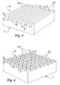
- the desired anti-reflection behaviour can be obtained both with a one-dimensional grating, i.e. with periodic projections along a single direction on the surface of the filament, both with a two-dimensional diffraction grating, i.e. with periodic projections along two orthogonal directions, not being necessarily parallel to each other, on the surface of the filament.
- the reference F designates a portion of an emitter which superficially has a diffraction grating R formed by periodic micro-projections R1 along a single direction; in the case shown in Figures 4 and 5, instead, the portion F of emitter according to the invention superficially has a diffraction grating R formed by periodic micro-projections R2 along two orthogonal directions.
- the anti-reflection structure R could have also different symmetries, such as a rhombic, hexagonal or any other type of symmetry.
- the reference h designates the depth or height of the projections R1, R2, the reference D designates the width of the projections and P the period of the grating R;
- the filling factor of the grating R is defined as the ratio D/P in the case of Figure 3, as the ratio D 2 /P 2 in the case of Figure 4 and as the ratio ⁇ D 2 /(4P 2 ) in the case of Figure 5.
- Figure 6 shows a portion F of an emitter whose superficial diffraction grating R is instead formed by micro-cavities C periodic along two orthogonal directions, being not necessarily parallel to each other; in substance, the .anti-reflection structure as proposed in Figure 6 has a shape that is complementary to the shape of the structure shown in Figure 5.
- the anti-reflection grating according to the invention can also be multi-level or with continuous profile, which allows to increase the degrees of freedom to optimise the grating and further enhance efficiency.
- the diffraction grating R is permanently encapsulated in a layer of refractory oxide, for instance yttrium oxide; the presence of said layer of oxide has many advantages:
- the microstructure R is therefore suitable to modify the spectral emissivity of the emitter F, increasing the portion of emitted visible light, and hence the luminous efficiency of the lamp or light source which incorporates said emitter.
- the micro-projections R1, R2 or the micro-cavities C will be conceived to maximise the electromagnetic emission in the visible spectrum from emitter F, without reducing and, in fact, possibly increasing reflectance in other spectral regions.
- the operation of the microstructure R is based on Kirchoff's law, according to which under thermal equilibrium conditions the electromagnetic radiation absorbed by a body at a specific wavelength is equal to the emitted electromagnetic radiation.
- a direction consequence of this law is that if the surface of a body has low spectral reflectance at a given wavelength, the corresponding spectral emissivity will be very high; vice versa, if spectral reflectance is high, the corresponding emissivity will be low.
- the dependence of spectral reflectance on the angle and on the polarisation state impacts on a similar angular dependency of spectral emissivity, based on the above considerations.
- the corresponding emission lobe will not be Lambertian (constant radiance, as in the case of unstructured source), but will follow the angular behaviour of the grating given by the microstructure R.
- the emitted radiation moreover, will have a degree of polarisation and coherence, unlike the radiation emitted by an incandescent source according to the prior art.
- a refractory oxide is used to encapsulate the filament provided with the grating, in such a way that the softening or even the passage to the liquid state of the nano-structured conductor material does not entail the destruction of the grating, and ultimately of the emitter.
- the refractory oxide which is non deformable at the temperature of incandescence of the emitter (1500K-2000K depending on the material) in fact constitutes a complementary matrix to the anti-reflection grating and it is therefore capable of maintaining the shape thereof even if the material constituting the emitter is deformed or liquefied. In this way, the performance of the grating is assured and the behaviour of the a priori designed emission is maintained, as explained above.
- the emitter or a part thereof is made with a conductor or semiconductor with low melting point, but having optical constants that are suitable significantly to enhance the efficiency of the emitter through an appropriate nanostructuring.
- Conductor material of particular interest in this sense are for instance gold, silver and copper.
- FIGS 11 and 12 are partial and schematic representations of two emitters F according to the present invention, which extend between respective electrodes H.
- the emitter F has an anti-reflection structure R of the type shown in Figure 5, constituted by substantially cylindrical micro-projections or pillars R2, whilst in the case of Figure 12 the structure R is of the type shown in Figure 6, constituted by micro-cavities C having circular cross section.
- the emitter F is structured in such a way as to obtain a two-dimensional phase grating, for instance made of gold, in which the electrical current that induces incandescence passes.
- the electrodes H are instead made of a high melting point conductor material, such as tungsten and the like, or semiconductor material, such as carbon and the like.
- the low melting point material of the emitter F traversed by current reaches: high temperature; for example, in the exemplified case, in which the material of interest is gold, the radiation is emitted by the emitter at an operating temperature around 1900-2000 degrees Kelvin. As previously explained, at such temperatures a gold grating would be liquefied.
- the layer of refractory oxide is provided, designated by the reference OR in Figures 11 and 12, which fully coats the emitter F, following its profile in its structured part R; in other words, the refractory oxide R is the perfect female 8 in the case of structure with micro-projections R2) or the perfect male (in the case of structure with micro-cavities C) of the grating R.
- the oxide OR with high melting temperature can for instance be a ceramic base oxide, thorium, cerium, yttrium, aluminium, zirconium oxide.
- the oxide matrix OR preserves the phase profile of the grating R, i.e. assures that its shape is maintained, even if the material constituting the emitter reaches the liquid state.
- one or more throats or cavities G are provided, open on the material of the emitter F; for example in correspondence with one or both electrodes as schematically shown in Figure 11, or within the refractory oxide structure, as schematically shown in Figure 12.
- Such cavities or throats G are provided to be filled by the material of the emitter F whose volume can expand at high temperatures; said throats G therefore serve to prevent delamination phenomena between the oxide OR and the material of the emitter F, as well as ruptures of the device.
- the micro-structure R. can be obtained directly from the material that constitutes the emitter F.
- a first possible method provides for the construction of a template made of porous alumina (porous aluminium oxide).
- a template made of porous alumina porous aluminium oxide
- an aluminium film with a thickness in the order of a micron, is plated by means of sputtering or thermal evaporation onto a suitable substrate, for example made of glass of silica, and it is subsequently subjected to an anodisation process.
- the process of anodising the aluminium film can be carried out using different electrolytic solutions depending on the size and distance of the alumina pores to be obtained.
- the layer of alumina obtained by means of the first anodisation of the aluminium film has an irregular structure; to obtain a highly regular structure, it becomes necessary to carry out successive anodisation processes, and in particular at least
- the etching step as per item ii) above is important to define on the residual part of irregular alumina preferential areas of growth of the alumina itself in the second anodisation step.
- the regular alumina template is obtained, it is infiltrated with the desired emitter material, for example by means of magnetron sputtering (DC or RF), i.e. in such a way that the alumina structure serves as a mould for the structured area of the emitter F.
- DC or RF magnetron sputtering
- the alumina structure can subsequently be eliminated in such a way as to be replaced with a refractory.oxide whose melting point is higher than alumina and which can be plated by means of RF sputtering.
- the alumina structure which is transparent, can be maintained, in order to assure that the shape of the grating R will be maintained at the operating temperatures of the emitter itself; in this case, on the part of the emitter F that is not structured and protected by the porous alumina will be plated a refractory oxide, in order to provide a globally closed container of the emitter material.
- Another possible manufacturing process starts from a filament, or from a planar lamina of the selected material, and etch the microstructure R under wavelength using any one of the known nanopatterning methods (electronic beam, or FIB or simple advanced photo lithography).
- the emitter thus obtained will be coated by refractory oxide, for instance by means of sputtering, CVD, electroplating.
- the emitter F according to the invention can be formed with multiple, mutually different materials.
- the basic material of the emitter can be a conductor with high melting point, for instance tungsten, designated as W, with the microstructure R obtained directly on said material; on said micro-structure is provided a thin and uniform coating of conductor or semiconductor material with low melting point and having more advantageous optical characteristics than tungsten, such as gold, designated by the reference Au; the coating Au allows to maintain the profile of the micro-projection R, whilst exploiting the more favourable emissivity properties of gold; the layer of refractory oxide OR enables to preserve the shape of the structure under conditions of operating temperature exceeding the melting temperature of the layer with low melting point Au.
- This embodiment also can be provided with a layer of refractory oxide OR on the layer of material W with high melting point, in order to prevent its evaporation and/or oxidation.
- the micro-structure R can be obtained on a layer of conductor or semiconductor material with low melting point, advantageous from the optical point of view, such as gold, designated by the reference Au, with said layer Au bearing the grating R obtained on a layer of conductor material with high melting point, such as tungsten, indicated by the reference W;
- a first layer OR of refractory oxide allows to preserve the shape of the microstructure R in conditions of operating temperature exceeding the melting temperature of the layer with low melting point Au in which the micro-structure itself is formed.
- a second layer of refractory oxide OR can be provided on the layer of material with high melting point W, in order to prevent its evaporation and/or oxidation.
- the micro-structure R can be obtained directly on a layer of refractory oxide OR; on the layer OR in which the structure R is formed is provided a thin, uniform coating of conductor or semiconductor material with low melting point, such as gold, designated by the reference Au; the layer Au obtained on the microstructure R formed in the oxide OR serves here directly as an emitter or carrier of electrical current; a second layer of refractory oxide OR which coats the layer Au allows to preserve the shape of the structure under conditions of operating temperature exceeding the melting temperature of the layer with low melting point.
- the emitter F described herein can be used to obtain incandescent light sources of various kinds, and in particular for the production of motor vehicle lighting devices.
- the invention is also suitable for application for the purpose of obtaining planar matrix of micro-sources of incandescent light, where the each of the latter is provided with a respective filament or emitter in accordance with the invention.
Landscapes
- Engineering & Computer Science (AREA)
- Manufacturing & Machinery (AREA)
- Resistance Heating (AREA)
- Circuit Arrangement For Electric Light Sources In General (AREA)
- Non-Portable Lighting Devices Or Systems Thereof (AREA)
- Luminescent Compositions (AREA)
Claims (28)
- Ein Emitter für Glühlichtquellen, der in der Lage ist, durch den Durchgang von elektrischem Strom zum Glühen gebracht zu werden, wobei auf zumindest einer Oberfläche des Emitters (F) eine Mikrostruktur (R) bereitgestellt wird, die wirksam ist, die Absorptionsfähigkeit für Wellenlängen, die zu dem sichtbaren Bereich des Spektrums gehören, zu erhöhen, dadurch gekennzeichnet, dass- die genannte Mikrostruktur (R) zumindest teilweise aus einem Material (W; Au; W, Au) gebildet ist, dessen Schmelztemperatur niedriger als eine Betriebstemperatur des Emitters (F) ist, und- zumindest ein wesentlicher Teil des Emitters (F), der die genannte Mikrostruktur (R) einschließt, mit einem feuerfesten Oxid (OR) oder einem Oxid mit einer hohen Schmelztemperatur beschichtet ist,wobei das genannte Oxid wirksam ist, ein Profil der genannten Mikrostruktur (R) in dem Fall der Deformation oder Zustandsänderung des genannten Materials (W; Au; W, Au) zu erhalten, die aus der Verwendung des Emitters (F) bei Betriebstemperaturen folgt, die die Schmelztemperatur des genannten Materials (W; Au; W, Au) überschreiten.
- Ein Emitter, wie in Anspruch 1 beansprucht, dadurch gekennzeichnet, dass das genannte Oxid (OR) wirksam ist, ein Profil der genannten Mikrostruktur (R) ebenso vor den Effekten des Verdampfens des jeweiligen Materials (W; Au; W, Au) zu schützen.
- Ein Emitter, wie in Anspruch 1 beansprucht, dadurch gekennzeichnet, dass der Emitter (F) beinahe vollständig, insbesondere mit Ausnahme von bestimmten Bereichen zur Verbindung mit Anschlüssen (H), mit dem genannten Oxid (OR) beschichtet ist.
- Ein Emitter, wie in Anspruch 1 beansprucht, dadurch gekennzeichnet, dass die genannte Mikrostruktur (R) aus einem Leiter, Halbleiter oder Verbundmaterial (W; Au; W, Au) hergestellt ist, dessen optische Konstanten in Kombination mit der Form der Mikrostruktur (R) so sind, dass eine höhere Leuchtemissionseffizienz als für ein klassisches Glühfilament ermöglicht wird, wobei die genannte Effizienz als das Verhältnis von dem Anteil der sichtbaren Strahlung, welcher bei der Betriebstemperatur in dem Bereich von 380 nm - 780 nm ausgestrahlt wird, und dem Anteil der Strahlung, welcher bei der selben Temperatur in dem Bereich von 380 nm - 2300 nm ausgestrahlt wird, definiert ist.
- Ein Emitter, wie in Anspruch 1 beansprucht, dadurch gekennzeichnet, dass das genannte Material (Au) aus einem Leiter, einem Halbleiter und einem Verbundmaterial ausgewählt wird, dessen Schmelztemperatur niedriger als die Betriebstemperatur des Filaments (F) ist.
- Ein Emitter, wie in Anspruch 1 beansprucht, dadurch gekennzeichnet, dass er aus zumindest einer ersten Schicht eines Leitermaterials (W), das bei einer höheren Temperatur als der Betriebstemperatur des Emitters (F) schmilzt, wie Wolfram, und einer zweiten Schicht eines Materials (Au), das aus einem Leiter, einem Halbleiter und einem Verbundmaterial ausgewählt wird, dessen Schmelztemperatur niedriger als die Betriebstemperatur des Emitters (F) ist, gebildet wird.
- Emitter, wie in Anspruch 1 beansprucht, dadurch gekennzeichnet, dass die genannte Mikrostruktur (R) zumindest teilweise aus einem Material gebildet wird, das aus Gold, Silber und Kupfer ausgewählt wird.
- Emitter, wie in Anspruch 1 beansprucht, dadurch gekennzeichnet, dass das genannte Oxid (OR) aus keramischen Basisoxiden, Thorium, Cerium, Yttrium, Aluminium oder Zirkoniumoxid ausgewählt wird.
- Ein Emitter, wie in Anspruch 1 beansprucht, dadurch gekennzeichnet, dass die genannte Mikrostruktur (R) mithilfe einer Oberflächenmikrostruktur des Emitters (F), d.h. mit dem selben Material, aus dem der Emitter gebildet ist, erhalten wird.
- Ein Emitter, wie in Anspruch 1 beansprucht, dadurch gekennzeichnet, dass die genannte Mikrostruktur ein Beugungsgitter (R) umfasst, das zumindest eine Mehrzahl von Mikrovorsprüngen (R1, R2) oder eine Mehrzahl von Mikrohohlräumen (C) aufweist, wobei die Abmessungen (h, D) der Mikrovorsprünge (R1, R2) oder der Mikrohohlräume (C) und die Periode (P) des Gitters (R) so sind, dass sie- die Emission sichtbarer elektromagnetischer Strahlung von dem Material (W; Au; W, Au), aus dem zumindest die Mikrostruktur (R) gebildet ist, erhöhen, und/oder- die Emission infraroter elektromagnetischer Strahlung von dem Material (W; Au; W, Au), aus dem zumindest die Mikrostruktur (R) gebildet ist, verringern, und/oder- die Emission der infraroten elektromagnetischen Strahlung von dem Material (W; Au; W, Au), aus dem zumindest die Mikrostruktur gebildet ist, zu einem geringeren Grade mit Hinsicht auf die Zunahme in dem sichtbaren Emissionsvermögen erhöhen.
- Ein Emitter, wie in Anspruch 10 beansprucht, dadurch gekennzeichnet, dass das genannte Gitter (R) erhalten wird durch ein- erstes Leitermaterial (W), das bei einer höheren Temperatur als der Betriebstemperatur des Emitters (F) schmilzt, wobei das erste Material einen strukturierten Teil besitzt,- eine Beschichtungslage (Au), die zumindest den strukturierten Teil des genannten ersten Materials (W) bedeckt, wobei die Beschichtungslage aus einem zweiten Material (Au) besteht, das aus einem Leiter, einem Halbleiter oder einem Verbundmaterial ausgewählt ist, der oder das bei einer niedrigeren Temperatur als der Betriebstemperatur des Emitters (F) schmilzt,wobei die Beschichtungslage (Au) hinreichend dünn ist, so dass sie das Profil des strukturierten Teils des ersten Materials (W) nachbildet, um damit das genannte Gitter (R) zu bilden, und das zweite Material (Au) eine größere Emissionseffizienz als das erste Material (W) besitzt, wobei die genannte Effizienz als das Verhältnis von dem Anteil der sichtbaren Strahlung, welcher bei der Betriebstemperatur in dem Bereich von 380 nm - 780 nm ausgestrahlt wird, und dem Anteil der Strahlung, welcher bei der selben Temperatur in dem Bereich von 380 nm - 2300 nm ausgestrahlt wird, definiert ist.
- Ein Emitter, wie in Anspruch 10 beansprucht, dadurch gekennzeichnet, dass- das genannte Gitter (R) auf der Oberfläche einer Schicht (Au) eines ersten Leiters, Halbleiters oder Verbundmaterials erhalten wird, dessen Schmelztemperatur niedriger als die Betriebstemperatur des Filaments (F) ist,- die genannte Schicht (Au) auf einem zweiten Leitermaterial (W) positioniert ist, dessen Schmelztemperatur höher als die Betriebstemperatur des Emittters (F) ist,wobei das erste Material (Au) eine größere Emissionseffizienz als das zweite Material (W) aufweist, wobei die genannte Effizienz als das Verhältnis von dem Anteil der sichtbaren Strahlung, welcher bei der Betriebstemperatur in dem Bereich von 380 nm - 780 nm ausgestrahlt wird, und dem Anteil der Strahlung, welcher bei der selben Temperatur in dem Bereich von 380 nm - 2300 nm ausgestrahlt wird, definiert ist.
- Ein Emitter, wie in Anspruch 10 beansprucht, dadurch gekennzeichnet, dass das genannte Gitter (R) erhalten wird durch- eine Schicht aus dem genannten Oxid (OR), das einen strukturierten Teil besitzt,- eine Beschichtungslage (Au), die zumindest den strukturierten Teil der genannten Schicht aus dem Oxid (OR) bedeckt, wobei die Beschichtungslage aus einem Material (Au) besteht, das aus einem Leiter, einem Halbleiter oder einem Verbundmaterial ausgewählt ist, der oder das bei einer niedrigeren Temperatur als der Betriebstemperatur des Emitters (F) schmilzt,wobei die Beschichtungslage (Au) hinreichend dünn ist, so dass sie das Profil des strukturierten Teils der genannten Schicht aus Oxid (OR) nachbildet, um damit das genannte Gitter (R) zu bilden, und wobei die Beschichtungslage (Au) wiederum durch eine Einkapselungsschicht beschichtet ist, die aus dem genannten Oxid (OR) gebildet ist.
- Ein Emitter, wie in Anspruch 3 beansprucht, dadurch gekennzeichnet, dass zumindest eine Kehlung oder ein Hohlraum (G) bereitgestellt wird, die oder der auf dem Material, das den Emitter (F) bildet, offen ist und in zumindest den genannten Elektroden (H) oder dem genannten Oxid (OR) ausgebildet ist, wobei der Hohlraum oder die Hohlräume (F), die bereitgestellt werden, so wirksam sind, dass sie einen Teil des genannten Materials als ein Ergebnis der Volumenausdehnungen desselben aufnehmen und/oder Ablösungsphänomene zwischen dem genannten Oxid (OR) und dem genannten Material und/oder Brüche des Komplexes, der durch das genannte Material, das genannte Oxid (OR) und die genannten Elektroden (H) gebildet wird, verhindern.
- Ein Emitter, wie in Anspruch 10 beansprucht, dadurch gekennzeichnet, dass die Periodizität der Mikrovorsprünge (R1, R2) oder der Mikrohohlräume (C) von der Ordnung der Wellenlänge der sichtbaren Strahlung ist.
- Ein Emitter, wie in Anspruch 10 beansprucht, dadurch gekennzeichnet, dass die Periodizität der Mikrovorsprünge (R1, R2) oder der Mikrohohlräume (C) zwischen 0,2 und 1 Mikron liegt.
- Ein Emitter, wie in Anspruch 10 beansprucht, dadurch gekennzeichnet, dass die Höhe oder Tiefe der Mikrovorsprünge (R1, R2) oder der Mikrohohlräume (C) zwischen 0,2 und 1 Mikron liegt.
- Ein Emitter, wie in Anspruch 1 beansprucht, dadurch gekennzeichnet, dass die genannte Mikrostruktur (R) binär, d.h. zwei Niveaus aufweisend, ist.
- Ein Emitter, wie in Anspruch 1 beansprucht, dadurch gekennzeichnet, dass die genannte Mikrostruktur (R) mehrere Niveaus aufweist, d.h. einen Vorsprung mit mehr als zwei Niveaus besitzt.
- Ein Emitter, wie in Anspruch 1 beansprucht, dadurch gekennzeichnet, dass die genannte Mikrostruktur (R) einen stufenlosen Vorsprung hat.
- Ein Emitter, wie in Anspruch 1 beansprucht, dadurch gekennzeichnet, dass er bei einer niedrigeren Temperatur als der Schmelztemperatur des genannten Oxids (OR) arbeitet.
- Ein Emitter, wie in Anspruch 1 beansprucht, dadurch gekennzeichnet, dass er als ein Filament oder ein ebenes Plättchen, das unter der Wellenlänge des sichtbaren Lichts strukturiert ist, konfiguriert ist, und dadurch, dass die genannte Mikrostruktur (R) ein zweidimensionales Gitter aus absorbierendem Material (k > 1) ist.
- Ein Verfahren zum Herstellen eines Emitters, der in der Lage ist, durch den Durchgang von elektrischem Strom zum Glühen gebracht zu werden, die Schritte umfassend:a) Bilden einer Vorlage aus porösem Aluminium;b) Infiltrieren der Vorlage aus porösem Aluminium mit einem Material, das bestimmt ist, den Emitter (F) zu bilden, auf eine solche Weise, dass die Aluminiumstruktur als eine Form für zumindest einen Teil einer Antireflexionsmikrostruktur (R) des Emitters (F) dient, wobei das genannte Material (Au) eine Schmelztemperatur besitzt, die niedriger als die Betriebstemperatur ist, bei der der Emitter (F) verwendet werden soll,c) Abscheiden eines feuerfesten Oxids (OR) auf den Teil des Emitters (F), der dazu bestimmt ist, sich zwischen zwei jeweiligen Anschlüssen (H) auszudehnen, wobei das genannte Oxid (OR) wirksam ist, ein Profil der genannten Mikrostruktur (R) in dem Fall der Deformation oder Zustandsänderung des jeweiligen Materials (Au) zu erhalten, die aus der Verwendung des Emitters (F) bei Betriebstemperaturen folgt, die die Schmelztemperatur des genannten Materials (Au) überschreiten,wobei die Vorlage aus porösem Aluminium beibehalten wird oder sonst vor dem Schritt c) entfernt wird.
- Ein Verfahren, wie in Anspruch 23 beansprucht, in dem der Schritt a) das Abscheiden eines Aluminiumfilms mit einer Dicke in der Ordnung von 1 Mikron auf einem geeigneten Substrat und die nachfolgende Anodisierung desselben umfasst, wobei die Anodisierung zumindest umfasst:- eine erste Phase der Anodisierung des Aluminiumfilms;- eine Phase des Reduzierens des ungleichmäßigen Aluminiumfilms, der als Ergebnis der ersten Anodisierungsphase erhalten wird;- eine zweite Phase der Anodisierung des Aluminiumfilms beginnend mit dem übriggebliebenen Teil des ungleichmäßigen Aluminiums, das durch die genannte Reduzierungsphase nicht entfernt worden ist.
- Ein Verfahren zum Herstellen eines Emitters, der in der Lage ist, durch den Durchgang von elektrischem Strom zum Glühen gebracht zu werden, die Schritte umfassend:- Bereitstellen eines dünnen oder plättchenartigen Elements des Materials, aus dem der Emitter (F) herzustellen ist, wobei das Material eine Schmelztemperatur besitzt, die niedriger als die Temperatur ist, bei der der Emitter (F) verwendet werden soll;- Ätzen des genannten Elements, um eine Antireflexionsmikrostruktur (R) auszubilden,und Beschichten des Emitters (F), in dem die Antireflexionsmikrostruktur (R) mit einem feuerfesten Oxid (OR) ausgebildet worden ist, wobei das genannte Oxid (OR) wirksam ist, ein Profil der genannten Mikrostruktur (R) in dem Fall der Deformation oder Zustandsänderung des jeweiligen Materials (Au) zu erhalten, die aus der Verwendung des Emitters (F) bei Betriebstemperaturen folgt, die die Schmelztemperatur des genannten Materials (Au) überschreiten.
- Eine Glühlichtquelle, die einen Lichtemitter umfasst, der in der Lage ist, durch den Durchgang von elektrischem Strom zum Glühen gebracht zu werden, dadurch gekennzeichnet, dass der genannte Emitter (F) so ist, wie es in einem oder mehreren der Ansprüche 1 bis 22 beansprucht ist.
- Eine Leuchtvorrichtung, insbesondere für Motorfahrzeuge, eine oder mehrere Lichtquellen (1), wie in Anspruch 26 beansprucht, umfassend.
- Eine ebene Matrix von Mikroquellen von Glühlicht, von denen jede jeweils einen Emitter (F) wie in einem oder mehreren der Ansprüche 1 bis 22 beansprucht umfasst.
Applications Claiming Priority (3)
| Application Number | Priority Date | Filing Date | Title |
|---|---|---|---|
| IT000166A ITTO20030166A1 (it) | 2003-03-06 | 2003-03-06 | Emettitore ad alta efficienza per sorgenti di luce ad incandescenza. |
| ITTO20030166 | 2003-03-06 | ||
| PCT/IB2004/000563 WO2004079773A2 (en) | 2003-03-06 | 2004-02-27 | High efficiency emitter for incandescent light sources |
Publications (2)
| Publication Number | Publication Date |
|---|---|
| EP1599892A2 EP1599892A2 (de) | 2005-11-30 |
| EP1599892B1 true EP1599892B1 (de) | 2006-12-27 |
Family
ID=32948214
Family Applications (1)
| Application Number | Title | Priority Date | Filing Date |
|---|---|---|---|
| EP04715406A Expired - Lifetime EP1599892B1 (de) | 2003-03-06 | 2004-02-27 | Glühkörper für lichtquellen mit hohem wirkungsgrad |
Country Status (10)
| Country | Link |
|---|---|
| US (1) | US7800290B2 (de) |
| EP (1) | EP1599892B1 (de) |
| JP (1) | JP2006520074A (de) |
| CN (1) | CN1748283A (de) |
| AT (1) | ATE349772T1 (de) |
| AU (1) | AU2003289669A1 (de) |
| DE (1) | DE602004003916T2 (de) |
| ES (1) | ES2277242T3 (de) |
| IT (1) | ITTO20030166A1 (de) |
| WO (2) | WO2004079897A2 (de) |
Families Citing this family (25)
| Publication number | Priority date | Publication date | Assignee | Title |
|---|---|---|---|---|
| US5876621A (en) * | 1997-09-30 | 1999-03-02 | Sapienza; Richard | Environmentally benign anti-icing or deicing fluids |
| KR100730144B1 (ko) * | 2005-08-30 | 2007-06-19 | 삼성에스디아이 주식회사 | 플라즈마 디스플레이 패널 |
| US8044567B2 (en) | 2006-03-31 | 2011-10-25 | General Electric Company | Light source incorporating a high temperature ceramic composite and gas phase for selective emission |
| US7722421B2 (en) * | 2006-03-31 | 2010-05-25 | General Electric Company | High temperature ceramic composite for selective emission |
| US20070228986A1 (en) * | 2006-03-31 | 2007-10-04 | General Electric Company | Light source incorporating a high temperature ceramic composite for selective emission |
| US7851985B2 (en) * | 2006-03-31 | 2010-12-14 | General Electric Company | Article incorporating a high temperature ceramic composite for selective emission |
| WO2007139022A1 (ja) * | 2006-05-26 | 2007-12-06 | Nalux Co., Ltd. | 赤外光源およびその製造方法 |
| GB0620883D0 (en) | 2006-10-20 | 2006-11-29 | Johnson Matthey Plc | Exhaust system for a lean-burn internal combustion engine |
| US7781977B2 (en) | 2006-12-20 | 2010-08-24 | General Electric Company | High temperature photonic structure for tungsten filament |
| US20090160314A1 (en) * | 2007-12-20 | 2009-06-25 | General Electric Company | Emissive structures and systems |
| US8138675B2 (en) * | 2009-02-27 | 2012-03-20 | General Electric Company | Stabilized emissive structures and methods of making |
| WO2013081127A1 (ja) * | 2011-12-01 | 2013-06-06 | スタンレー電気株式会社 | 光源装置、および、フィラメント |
| JP2013134875A (ja) | 2011-12-26 | 2013-07-08 | Stanley Electric Co Ltd | 白熱電球、および、フィラメント |
| JP5964581B2 (ja) * | 2011-12-26 | 2016-08-03 | スタンレー電気株式会社 | 白熱電球 |
| US9709349B2 (en) * | 2012-11-15 | 2017-07-18 | The Board Of Trustees Of The Leland Stanford Junior University | Structures for radiative cooling |
| US10955596B1 (en) * | 2013-03-15 | 2021-03-23 | Wavefront Research, Inc. | Nanofabricated volume gratings |
| JP6239839B2 (ja) * | 2013-03-22 | 2017-11-29 | スタンレー電気株式会社 | 光源装置、および、フィラメント |
| FR3055738B1 (fr) * | 2016-09-05 | 2018-09-07 | Commissariat A L'energie Atomique Et Aux Energies Alternatives | Surface d'emission de rayonnement infrarouge ir a emissivite thermique elevee et a grande duree de vie et son procede de fabrication |
| US10797633B2 (en) | 2016-11-10 | 2020-10-06 | Mitsubishi Electric Research Laboratories, Inc. | Thermal emitter for energy conversion technical field |
| CN110031114A (zh) * | 2018-01-11 | 2019-07-19 | 清华大学 | 面源黑体 |
| EP3903044A1 (de) | 2018-12-27 | 2021-11-03 | Skycool Systems, Inc. | Kühlplattensystem |
| US11359841B2 (en) | 2019-04-17 | 2022-06-14 | SkyCool Systems, Inc. | Radiative cooling systems |
| CN116232457B (zh) * | 2023-05-06 | 2023-07-28 | 武汉工程大学 | 可调制发射率的红外发射器及红外发射器系统 |
| CN117645413A (zh) * | 2023-11-29 | 2024-03-05 | 玻璃新材料创新中心(安徽)有限公司 | 一种日间辐射冷却玻璃及其制备方法和应用 |
| EP4654248A1 (de) * | 2024-05-22 | 2025-11-26 | 4K-Mems Sa | Temperatur- und/oder strahlungsintensitätsstandard |
Family Cites Families (22)
| Publication number | Priority date | Publication date | Assignee | Title |
|---|---|---|---|---|
| US2077633A (en) * | 1930-06-14 | 1937-04-20 | G M Laberateries Inc | Photoelectric tube |
| US2603669A (en) * | 1948-10-26 | 1952-07-15 | Union Carbide & Carbon Corp | Large electrode with thermal stress relief |
| FR1439722A (fr) * | 1965-07-13 | 1966-05-20 | Philips Nv | Lampe électrique à incandescence utilisant un filament à rayonnement sélectif |
| NL7400762A (nl) * | 1974-01-21 | 1975-07-23 | Philips Nv | Electrische gloeilamp. |
| US4196368A (en) * | 1977-09-07 | 1980-04-01 | Eikonix Corporation | Improving incandescent bulb efficiency |
| GB2032173B (en) * | 1978-10-10 | 1982-11-24 | Gen Electric Co Ltd | Electric incandescent lamps |
| US4499398A (en) * | 1982-06-08 | 1985-02-12 | Munroe Ronald G | Incandescent lighting |
| US4864186A (en) * | 1988-03-29 | 1989-09-05 | Milewski John V | Single crystal whisker electric light filament |
| US5079473A (en) * | 1989-09-08 | 1992-01-07 | John F. Waymouth Intellectual Property And Education Trust | Optical light source device |
| US5152870A (en) * | 1991-01-22 | 1992-10-06 | General Electric Company | Method for producing lamp filaments of increased radiative efficiency |
| US5389853A (en) * | 1992-10-01 | 1995-02-14 | General Electric Company | Incandescent lamp filament with surface crystallites and method of formation |
| US5416376A (en) * | 1992-10-29 | 1995-05-16 | The Regents Of The University Of California | Aerogel-supported filament |
| US5814840A (en) * | 1995-06-06 | 1998-09-29 | Purdue Research Foundation | Incandescent light energy conversion with reduced infrared emission |
| US5955839A (en) * | 1997-03-26 | 1999-09-21 | Quantum Vision, Inc. | Incandescent microcavity lightsource having filament spaced from reflector at node of wave emitted |
| US6281629B1 (en) * | 1997-11-26 | 2001-08-28 | Ushiodenki Kabushiki Kaisha | Short arc lamp having heat transferring plate and specific connector structure between cathode and electrode support |
| DE19845423A1 (de) * | 1998-10-02 | 2000-04-13 | Fraunhofer Ges Forschung | Heißer Strahler |
| US6607673B2 (en) * | 2000-05-17 | 2003-08-19 | The University Of Tokyo | Method for manufacturing a diamond cylinder array having dents therein |
| ITTO20010341A1 (it) * | 2001-04-10 | 2002-10-10 | Fiat Ricerche | Sorgente di luce a matrice di microfilamenti. |
| US6768256B1 (en) * | 2001-08-27 | 2004-07-27 | Sandia Corporation | Photonic crystal light source |
| US6611085B1 (en) * | 2001-08-27 | 2003-08-26 | Sandia Corporation | Photonically engineered incandescent emitter |
| DE10240056B4 (de) * | 2002-08-30 | 2005-06-23 | Fraunhofer-Gesellschaft zur Förderung der angewandten Forschung e.V. | Hochtemperaturstabiler Metallemitter sowie Verfahren zur Herstellung |
| ITTO20030167A1 (it) * | 2003-03-06 | 2004-09-07 | Fiat Ricerche | Procedimento per la realizzazione di emettitori nano-strutturati per sorgenti di luce ad incandescenza. |
-
2003
- 2003-03-06 IT IT000166A patent/ITTO20030166A1/it unknown
- 2003-12-23 WO PCT/IB2003/006313 patent/WO2004079897A2/en not_active Ceased
- 2003-12-23 AU AU2003289669A patent/AU2003289669A1/en not_active Abandoned
-
2004
- 2004-02-27 WO PCT/IB2004/000563 patent/WO2004079773A2/en not_active Ceased
- 2004-02-27 DE DE602004003916T patent/DE602004003916T2/de not_active Expired - Lifetime
- 2004-02-27 CN CNA200480001208XA patent/CN1748283A/zh active Pending
- 2004-02-27 US US10/534,389 patent/US7800290B2/en not_active Expired - Fee Related
- 2004-02-27 AT AT04715406T patent/ATE349772T1/de not_active IP Right Cessation
- 2004-02-27 ES ES04715406T patent/ES2277242T3/es not_active Expired - Lifetime
- 2004-02-27 EP EP04715406A patent/EP1599892B1/de not_active Expired - Lifetime
- 2004-02-27 JP JP2006506282A patent/JP2006520074A/ja not_active Withdrawn
Also Published As
| Publication number | Publication date |
|---|---|
| JP2006520074A (ja) | 2006-08-31 |
| US7800290B2 (en) | 2010-09-21 |
| WO2004079773A3 (en) | 2005-01-13 |
| WO2004079773A2 (en) | 2004-09-16 |
| ITTO20030166A1 (it) | 2004-09-07 |
| WO2004079897A2 (en) | 2004-09-16 |
| CN1748283A (zh) | 2006-03-15 |
| WO2004079897A3 (en) | 2004-12-29 |
| DE602004003916T2 (de) | 2007-06-14 |
| DE602004003916D1 (de) | 2007-02-08 |
| AU2003289669A1 (en) | 2004-09-28 |
| US20060076868A1 (en) | 2006-04-13 |
| ES2277242T3 (es) | 2007-07-01 |
| ATE349772T1 (de) | 2007-01-15 |
| AU2003289669A8 (en) | 2004-09-28 |
| EP1599892A2 (de) | 2005-11-30 |
Similar Documents
| Publication | Publication Date | Title |
|---|---|---|
| US7800290B2 (en) | High efficiency emitter for incandescent light sources | |
| JP5689934B2 (ja) | 光源 | |
| JP2005501383A5 (de) | ||
| EP2005464A1 (de) | Lichtquellen mit einem keramischen hochtemperaturverbundstoff und gasphase zur selektiven emission | |
| JP2005501383A (ja) | フォトニクス加工白熱発光体 | |
| WO2007126696A1 (en) | High temperature ceramic composite for selective emission | |
| US9214330B2 (en) | Light source device and filament | |
| EP2787524B1 (de) | Lichtquellenvorrichtung und filament | |
| EP1249856A2 (de) | Lichtquelle mit einer Matrix von Mikrofilamenten | |
| US7851985B2 (en) | Article incorporating a high temperature ceramic composite for selective emission | |
| JP2003508875A (ja) | 光源および光源を製造する方法 | |
| US4196368A (en) | Improving incandescent bulb efficiency | |
| US20070228986A1 (en) | Light source incorporating a high temperature ceramic composite for selective emission | |
| Lunk | Incandescent lighting and powder metallurgical manufacturing of tungsten wire | |
| WO2008079564A2 (en) | High temperature photonic structure for tungsten filament | |
| JP2016015260A (ja) | フィラメント、それを用いた光源、および、フィラメントの製造方法 | |
| CAPELLO et al. | GLÜHKÖRPER FÜR LICHTQUELLEN MIT HOHEM WIRKUNGSGRAD EMETTEUR A EFFICACITE ELEVEE POUR SOURCES D’ECLAIRAGE A INCANDESCENCE | |
| JP6153734B2 (ja) | 光源装置 | |
| JP6239839B2 (ja) | 光源装置、および、フィラメント | |
| WO2009045605A2 (en) | Thermo-optically functional compositions, systems and methods of making | |
| Dawson et al. | The Incandescent Lamp | |
| JP6625902B2 (ja) | 発光体、フィラメント、フィラメントを用いた装置、および、白熱電球 | |
| JP2014164866A (ja) | フィラメント、および、その製造方法 | |
| JP2007234362A (ja) | 白熱電球および白熱電球の製造方法 |
Legal Events
| Date | Code | Title | Description |
|---|---|---|---|
| PUAI | Public reference made under article 153(3) epc to a published international application that has entered the european phase |
Free format text: ORIGINAL CODE: 0009012 |
|
| 17P | Request for examination filed |
Effective date: 20050523 |
|
| AK | Designated contracting states |
Kind code of ref document: A2 Designated state(s): AT BE BG CH CY CZ DE DK EE ES FI FR GB GR HU IE IT LI LU MC NL PT RO SE SI SK TR |
|
| AX | Request for extension of the european patent |
Extension state: AL LT LV MK |
|
| DAX | Request for extension of the european patent (deleted) | ||
| GRAP | Despatch of communication of intention to grant a patent |
Free format text: ORIGINAL CODE: EPIDOSNIGR1 |
|
| GRAS | Grant fee paid |
Free format text: ORIGINAL CODE: EPIDOSNIGR3 |
|
| GRAA | (expected) grant |
Free format text: ORIGINAL CODE: 0009210 |
|
| AK | Designated contracting states |
Kind code of ref document: B1 Designated state(s): AT BE BG CH CY CZ DE DK EE ES FI FR GB GR HU IE IT LI LU MC NL PT RO SE SI SK TR |
|
| PG25 | Lapsed in a contracting state [announced via postgrant information from national office to epo] |
Ref country code: CH Free format text: LAPSE BECAUSE OF FAILURE TO SUBMIT A TRANSLATION OF THE DESCRIPTION OR TO PAY THE FEE WITHIN THE PRESCRIBED TIME-LIMIT Effective date: 20061227 Ref country code: SI Free format text: LAPSE BECAUSE OF FAILURE TO SUBMIT A TRANSLATION OF THE DESCRIPTION OR TO PAY THE FEE WITHIN THE PRESCRIBED TIME-LIMIT Effective date: 20061227 Ref country code: AT Free format text: LAPSE BECAUSE OF FAILURE TO SUBMIT A TRANSLATION OF THE DESCRIPTION OR TO PAY THE FEE WITHIN THE PRESCRIBED TIME-LIMIT Effective date: 20061227 Ref country code: LI Free format text: LAPSE BECAUSE OF FAILURE TO SUBMIT A TRANSLATION OF THE DESCRIPTION OR TO PAY THE FEE WITHIN THE PRESCRIBED TIME-LIMIT Effective date: 20061227 Ref country code: CZ Free format text: LAPSE BECAUSE OF FAILURE TO SUBMIT A TRANSLATION OF THE DESCRIPTION OR TO PAY THE FEE WITHIN THE PRESCRIBED TIME-LIMIT Effective date: 20061227 Ref country code: RO Free format text: LAPSE BECAUSE OF FAILURE TO SUBMIT A TRANSLATION OF THE DESCRIPTION OR TO PAY THE FEE WITHIN THE PRESCRIBED TIME-LIMIT Effective date: 20061227 Ref country code: SK Free format text: LAPSE BECAUSE OF FAILURE TO SUBMIT A TRANSLATION OF THE DESCRIPTION OR TO PAY THE FEE WITHIN THE PRESCRIBED TIME-LIMIT Effective date: 20061227 Ref country code: BE Free format text: LAPSE BECAUSE OF FAILURE TO SUBMIT A TRANSLATION OF THE DESCRIPTION OR TO PAY THE FEE WITHIN THE PRESCRIBED TIME-LIMIT Effective date: 20061227 Ref country code: NL Free format text: LAPSE BECAUSE OF FAILURE TO SUBMIT A TRANSLATION OF THE DESCRIPTION OR TO PAY THE FEE WITHIN THE PRESCRIBED TIME-LIMIT Effective date: 20061227 Ref country code: FI Free format text: LAPSE BECAUSE OF FAILURE TO SUBMIT A TRANSLATION OF THE DESCRIPTION OR TO PAY THE FEE WITHIN THE PRESCRIBED TIME-LIMIT Effective date: 20061227 Ref country code: DK Free format text: LAPSE BECAUSE OF FAILURE TO SUBMIT A TRANSLATION OF THE DESCRIPTION OR TO PAY THE FEE WITHIN THE PRESCRIBED TIME-LIMIT Effective date: 20061227 |
|
| REG | Reference to a national code |
Ref country code: GB Ref legal event code: FG4D |
|
| REG | Reference to a national code |
Ref country code: SE Ref legal event code: TRGR |
|
| REG | Reference to a national code |
Ref country code: IE Ref legal event code: FG4D |
|
| REF | Corresponds to: |
Ref document number: 602004003916 Country of ref document: DE Date of ref document: 20070208 Kind code of ref document: P |
|
| PG25 | Lapsed in a contracting state [announced via postgrant information from national office to epo] |
Ref country code: MC Free format text: LAPSE BECAUSE OF NON-PAYMENT OF DUE FEES Effective date: 20070228 |
|
| PG25 | Lapsed in a contracting state [announced via postgrant information from national office to epo] |
Ref country code: BG Free format text: LAPSE BECAUSE OF FAILURE TO SUBMIT A TRANSLATION OF THE DESCRIPTION OR TO PAY THE FEE WITHIN THE PRESCRIBED TIME-LIMIT Effective date: 20070327 |
|
| PG25 | Lapsed in a contracting state [announced via postgrant information from national office to epo] |
Ref country code: PT Free format text: LAPSE BECAUSE OF FAILURE TO SUBMIT A TRANSLATION OF THE DESCRIPTION OR TO PAY THE FEE WITHIN THE PRESCRIBED TIME-LIMIT Effective date: 20070528 |
|
| NLV1 | Nl: lapsed or annulled due to failure to fulfill the requirements of art. 29p and 29m of the patents act | ||
| ET | Fr: translation filed | ||
| REG | Reference to a national code |
Ref country code: CH Ref legal event code: PL |
|
| REG | Reference to a national code |
Ref country code: ES Ref legal event code: FG2A Ref document number: 2277242 Country of ref document: ES Kind code of ref document: T3 |
|
| PLBE | No opposition filed within time limit |
Free format text: ORIGINAL CODE: 0009261 |
|
| STAA | Information on the status of an ep patent application or granted ep patent |
Free format text: STATUS: NO OPPOSITION FILED WITHIN TIME LIMIT |
|
| 26N | No opposition filed |
Effective date: 20070928 |
|
| PG25 | Lapsed in a contracting state [announced via postgrant information from national office to epo] |
Ref country code: IE Free format text: LAPSE BECAUSE OF NON-PAYMENT OF DUE FEES Effective date: 20070227 |
|
| PG25 | Lapsed in a contracting state [announced via postgrant information from national office to epo] |
Ref country code: GR Free format text: LAPSE BECAUSE OF FAILURE TO SUBMIT A TRANSLATION OF THE DESCRIPTION OR TO PAY THE FEE WITHIN THE PRESCRIBED TIME-LIMIT Effective date: 20070328 |
|
| PGFP | Annual fee paid to national office [announced via postgrant information from national office to epo] |
Ref country code: ES Payment date: 20080324 Year of fee payment: 5 |
|
| PGFP | Annual fee paid to national office [announced via postgrant information from national office to epo] |
Ref country code: SE Payment date: 20080219 Year of fee payment: 5 |
|
| PGFP | Annual fee paid to national office [announced via postgrant information from national office to epo] |
Ref country code: FR Payment date: 20080208 Year of fee payment: 5 |
|
| PG25 | Lapsed in a contracting state [announced via postgrant information from national office to epo] |
Ref country code: EE Free format text: LAPSE BECAUSE OF FAILURE TO SUBMIT A TRANSLATION OF THE DESCRIPTION OR TO PAY THE FEE WITHIN THE PRESCRIBED TIME-LIMIT Effective date: 20061227 |
|
| PG25 | Lapsed in a contracting state [announced via postgrant information from national office to epo] |
Ref country code: CY Free format text: LAPSE BECAUSE OF FAILURE TO SUBMIT A TRANSLATION OF THE DESCRIPTION OR TO PAY THE FEE WITHIN THE PRESCRIBED TIME-LIMIT Effective date: 20061227 Ref country code: LU Free format text: LAPSE BECAUSE OF NON-PAYMENT OF DUE FEES Effective date: 20070227 |
|
| PG25 | Lapsed in a contracting state [announced via postgrant information from national office to epo] |
Ref country code: HU Free format text: LAPSE BECAUSE OF FAILURE TO SUBMIT A TRANSLATION OF THE DESCRIPTION OR TO PAY THE FEE WITHIN THE PRESCRIBED TIME-LIMIT Effective date: 20070628 Ref country code: TR Free format text: LAPSE BECAUSE OF FAILURE TO SUBMIT A TRANSLATION OF THE DESCRIPTION OR TO PAY THE FEE WITHIN THE PRESCRIBED TIME-LIMIT Effective date: 20061227 |
|
| EUG | Se: european patent has lapsed | ||
| REG | Reference to a national code |
Ref country code: FR Ref legal event code: ST Effective date: 20091030 |
|
| REG | Reference to a national code |
Ref country code: ES Ref legal event code: FD2A Effective date: 20090228 |
|
| PG25 | Lapsed in a contracting state [announced via postgrant information from national office to epo] |
Ref country code: FR Free format text: LAPSE BECAUSE OF NON-PAYMENT OF DUE FEES Effective date: 20090302 |
|
| PG25 | Lapsed in a contracting state [announced via postgrant information from national office to epo] |
Ref country code: ES Free format text: LAPSE BECAUSE OF NON-PAYMENT OF DUE FEES Effective date: 20090228 |
|
| PG25 | Lapsed in a contracting state [announced via postgrant information from national office to epo] |
Ref country code: SE Free format text: LAPSE BECAUSE OF NON-PAYMENT OF DUE FEES Effective date: 20090228 |
|
| PGFP | Annual fee paid to national office [announced via postgrant information from national office to epo] |
Ref country code: DE Payment date: 20110223 Year of fee payment: 8 Ref country code: IT Payment date: 20110208 Year of fee payment: 8 |
|
| PGFP | Annual fee paid to national office [announced via postgrant information from national office to epo] |
Ref country code: GB Payment date: 20110223 Year of fee payment: 8 |
|
| GBPC | Gb: european patent ceased through non-payment of renewal fee |
Effective date: 20120227 |
|
| PG25 | Lapsed in a contracting state [announced via postgrant information from national office to epo] |
Ref country code: IT Free format text: LAPSE BECAUSE OF NON-PAYMENT OF DUE FEES Effective date: 20120227 |
|
| REG | Reference to a national code |
Ref country code: DE Ref legal event code: R119 Ref document number: 602004003916 Country of ref document: DE Effective date: 20120901 |
|
| PG25 | Lapsed in a contracting state [announced via postgrant information from national office to epo] |
Ref country code: GB Free format text: LAPSE BECAUSE OF NON-PAYMENT OF DUE FEES Effective date: 20120227 |
|
| PG25 | Lapsed in a contracting state [announced via postgrant information from national office to epo] |
Ref country code: DE Free format text: LAPSE BECAUSE OF NON-PAYMENT OF DUE FEES Effective date: 20120901 |