EP1598909B1 - Semiconductor device having quantum well structure, and method of forming the same - Google Patents
Semiconductor device having quantum well structure, and method of forming the same Download PDFInfo
- Publication number
- EP1598909B1 EP1598909B1 EP05002169A EP05002169A EP1598909B1 EP 1598909 B1 EP1598909 B1 EP 1598909B1 EP 05002169 A EP05002169 A EP 05002169A EP 05002169 A EP05002169 A EP 05002169A EP 1598909 B1 EP1598909 B1 EP 1598909B1
- Authority
- EP
- European Patent Office
- Prior art keywords
- temperature
- film
- barrier
- barrier film
- semiconductor
- Prior art date
- Legal status (The legal status is an assumption and is not a legal conclusion. Google has not performed a legal analysis and makes no representation as to the accuracy of the status listed.)
- Expired - Fee Related
Links
- 239000004065 semiconductor Substances 0.000 title claims description 338
- 238000000034 method Methods 0.000 title claims description 87
- 230000004888 barrier function Effects 0.000 claims description 387
- APFVFJFRJDLVQX-UHFFFAOYSA-N indium atom Chemical compound [In] APFVFJFRJDLVQX-UHFFFAOYSA-N 0.000 claims description 73
- 229910052738 indium Inorganic materials 0.000 claims description 70
- IJGRMHOSHXDMSA-UHFFFAOYSA-N Atomic nitrogen Chemical compound N#N IJGRMHOSHXDMSA-UHFFFAOYSA-N 0.000 claims description 62
- 150000004767 nitrides Chemical class 0.000 claims description 48
- 239000000203 mixture Substances 0.000 claims description 40
- 238000000151 deposition Methods 0.000 claims description 32
- GYHNNYVSQQEPJS-UHFFFAOYSA-N Gallium Chemical compound [Ga] GYHNNYVSQQEPJS-UHFFFAOYSA-N 0.000 claims description 31
- 229910052733 gallium Inorganic materials 0.000 claims description 31
- 229910052757 nitrogen Inorganic materials 0.000 claims description 31
- 230000015572 biosynthetic process Effects 0.000 description 41
- 229910002601 GaN Inorganic materials 0.000 description 35
- 239000013078 crystal Substances 0.000 description 35
- 238000005036 potential barrier Methods 0.000 description 26
- JMASRVWKEDWRBT-UHFFFAOYSA-N Gallium nitride Chemical compound [Ga]#N JMASRVWKEDWRBT-UHFFFAOYSA-N 0.000 description 17
- 230000003287 optical effect Effects 0.000 description 17
- 230000008859 change Effects 0.000 description 13
- 239000007789 gas Substances 0.000 description 13
- 150000001875 compounds Chemical class 0.000 description 12
- 230000000630 rising effect Effects 0.000 description 12
- 238000005253 cladding Methods 0.000 description 11
- 239000000758 substrate Substances 0.000 description 11
- 125000004429 atom Chemical group 0.000 description 10
- 229910002704 AlGaN Inorganic materials 0.000 description 7
- 230000007547 defect Effects 0.000 description 7
- 238000004519 manufacturing process Methods 0.000 description 7
- 230000005012 migration Effects 0.000 description 7
- 238000013508 migration Methods 0.000 description 7
- 238000011109 contamination Methods 0.000 description 6
- 238000000089 atomic force micrograph Methods 0.000 description 4
- 239000000470 constituent Substances 0.000 description 4
- 230000007423 decrease Effects 0.000 description 4
- 238000002073 fluorescence micrograph Methods 0.000 description 4
- QGZKDVFQNNGYKY-UHFFFAOYSA-N Ammonia Chemical compound N QGZKDVFQNNGYKY-UHFFFAOYSA-N 0.000 description 3
- 230000015556 catabolic process Effects 0.000 description 3
- 238000000354 decomposition reaction Methods 0.000 description 3
- 238000006731 degradation reaction Methods 0.000 description 3
- 238000005204 segregation Methods 0.000 description 3
- 229910052782 aluminium Inorganic materials 0.000 description 2
- XAGFODPZIPBFFR-UHFFFAOYSA-N aluminium Chemical compound [Al] XAGFODPZIPBFFR-UHFFFAOYSA-N 0.000 description 2
- 230000008021 deposition Effects 0.000 description 2
- 230000006866 deterioration Effects 0.000 description 2
- 238000010586 diagram Methods 0.000 description 2
- 239000001257 hydrogen Substances 0.000 description 2
- 229910052739 hydrogen Inorganic materials 0.000 description 2
- 125000004435 hydrogen atom Chemical class [H]* 0.000 description 2
- 230000006872 improvement Effects 0.000 description 2
- 238000005259 measurement Methods 0.000 description 2
- 238000012986 modification Methods 0.000 description 2
- 230000004048 modification Effects 0.000 description 2
- 238000007669 thermal treatment Methods 0.000 description 2
- 230000002411 adverse Effects 0.000 description 1
- 229910021529 ammonia Inorganic materials 0.000 description 1
- 239000000969 carrier Substances 0.000 description 1
- 239000012159 carrier gas Substances 0.000 description 1
- 238000004140 cleaning Methods 0.000 description 1
- 230000000052 comparative effect Effects 0.000 description 1
- 238000003795 desorption Methods 0.000 description 1
- 238000011156 evaluation Methods 0.000 description 1
- 230000005284 excitation Effects 0.000 description 1
- 230000001747 exhibiting effect Effects 0.000 description 1
- 239000000463 material Substances 0.000 description 1
- 229910000069 nitrogen hydride Inorganic materials 0.000 description 1
- 125000002524 organometallic group Chemical group 0.000 description 1
- 238000004904 shortening Methods 0.000 description 1
- 229910052710 silicon Inorganic materials 0.000 description 1
- 239000010703 silicon Substances 0.000 description 1
- 238000009751 slip forming Methods 0.000 description 1
- 230000006641 stabilisation Effects 0.000 description 1
- 238000011105 stabilization Methods 0.000 description 1
- 230000000087 stabilizing effect Effects 0.000 description 1
- 238000000927 vapour-phase epitaxy Methods 0.000 description 1
Images


Classifications
-
- H—ELECTRICITY
- H10—SEMICONDUCTOR DEVICES; ELECTRIC SOLID-STATE DEVICES NOT OTHERWISE PROVIDED FOR
- H10H—INORGANIC LIGHT-EMITTING SEMICONDUCTOR DEVICES HAVING POTENTIAL BARRIERS
- H10H20/00—Individual inorganic light-emitting semiconductor devices having potential barriers, e.g. light-emitting diodes [LED]
- H10H20/80—Constructional details
- H10H20/81—Bodies
- H10H20/822—Materials of the light-emitting regions
- H10H20/824—Materials of the light-emitting regions comprising only Group III-V materials, e.g. GaP
- H10H20/825—Materials of the light-emitting regions comprising only Group III-V materials, e.g. GaP containing nitrogen, e.g. GaN
-
- B—PERFORMING OPERATIONS; TRANSPORTING
- B82—NANOTECHNOLOGY
- B82Y—SPECIFIC USES OR APPLICATIONS OF NANOSTRUCTURES; MEASUREMENT OR ANALYSIS OF NANOSTRUCTURES; MANUFACTURE OR TREATMENT OF NANOSTRUCTURES
- B82Y20/00—Nanooptics, e.g. quantum optics or photonic crystals
-
- H—ELECTRICITY
- H01—ELECTRIC ELEMENTS
- H01S—DEVICES USING THE PROCESS OF LIGHT AMPLIFICATION BY STIMULATED EMISSION OF RADIATION [LASER] TO AMPLIFY OR GENERATE LIGHT; DEVICES USING STIMULATED EMISSION OF ELECTROMAGNETIC RADIATION IN WAVE RANGES OTHER THAN OPTICAL
- H01S5/00—Semiconductor lasers
- H01S5/30—Structure or shape of the active region; Materials used for the active region
- H01S5/34—Structure or shape of the active region; Materials used for the active region comprising quantum well or superlattice structures, e.g. single quantum well [SQW] lasers, multiple quantum well [MQW] lasers or graded index separate confinement heterostructure [GRINSCH] lasers
- H01S5/343—Structure or shape of the active region; Materials used for the active region comprising quantum well or superlattice structures, e.g. single quantum well [SQW] lasers, multiple quantum well [MQW] lasers or graded index separate confinement heterostructure [GRINSCH] lasers in AIIIBV compounds, e.g. AlGaAs-laser, InP-based laser
- H01S5/34333—Structure or shape of the active region; Materials used for the active region comprising quantum well or superlattice structures, e.g. single quantum well [SQW] lasers, multiple quantum well [MQW] lasers or graded index separate confinement heterostructure [GRINSCH] lasers in AIIIBV compounds, e.g. AlGaAs-laser, InP-based laser with a well layer based on Ga(In)N or Ga(In)P, e.g. blue laser
-
- H—ELECTRICITY
- H10—SEMICONDUCTOR DEVICES; ELECTRIC SOLID-STATE DEVICES NOT OTHERWISE PROVIDED FOR
- H10H—INORGANIC LIGHT-EMITTING SEMICONDUCTOR DEVICES HAVING POTENTIAL BARRIERS
- H10H20/00—Individual inorganic light-emitting semiconductor devices having potential barriers, e.g. light-emitting diodes [LED]
- H10H20/80—Constructional details
- H10H20/81—Bodies
- H10H20/811—Bodies having quantum effect structures or superlattices, e.g. tunnel junctions
- H10H20/812—Bodies having quantum effect structures or superlattices, e.g. tunnel junctions within the light-emitting regions, e.g. having quantum confinement structures
-
- H—ELECTRICITY
- H01—ELECTRIC ELEMENTS
- H01S—DEVICES USING THE PROCESS OF LIGHT AMPLIFICATION BY STIMULATED EMISSION OF RADIATION [LASER] TO AMPLIFY OR GENERATE LIGHT; DEVICES USING STIMULATED EMISSION OF ELECTROMAGNETIC RADIATION IN WAVE RANGES OTHER THAN OPTICAL
- H01S5/00—Semiconductor lasers
- H01S5/30—Structure or shape of the active region; Materials used for the active region
- H01S5/34—Structure or shape of the active region; Materials used for the active region comprising quantum well or superlattice structures, e.g. single quantum well [SQW] lasers, multiple quantum well [MQW] lasers or graded index separate confinement heterostructure [GRINSCH] lasers
- H01S5/3407—Structure or shape of the active region; Materials used for the active region comprising quantum well or superlattice structures, e.g. single quantum well [SQW] lasers, multiple quantum well [MQW] lasers or graded index separate confinement heterostructure [GRINSCH] lasers characterised by special barrier layers
Definitions
- the present invention relates to a semiconductor device having a quantum well structure and to a method of forming the same.
- Document 1 Japanese Patent Application Laid-Open No. 2001-168471 discloses a nitride semiconductor laser diode having a active layer with the quantum well structure.
- the active layer has intermediate layers each of which is provided between one of well layers and one of barrier layers in the active layer.
- the intermediate layers are made of Al d Ga 1-d N (0.30 ⁇ d ⁇ 1) and the bandgap energy of the intermediate layers is greater than that of the barrier layers.
- the addition of the intermediate layers can decrease the threshold voltage and driving voltage of the nitride semiconductor laser diode.
- This nitride semiconductor laser diode improves the luminous efficiency thereof by use of the AlGaN intermediate layers, which has a bandgap energy larger than that of the barrier layers, between the well layers and the barrier layers of nitride semiconductors containing indium.
- Document 2 Japanese Patent Application Laid-Open No. 10-84132 discloses semiconductor light emitting devices such as a semiconductor laser and a light emitting diode.
- the semiconductor light emitting devices have a light generating region with a superlattice structure.
- This light generating layer includes quantum well layers, barrier layers and buffer layers. Each buffer layer is located between one of the quantum well layers and one of the barrier layers. Potential barrier between the quantum well layers and the buffer layers is smaller than potential barrier between the quantum well layers and the barrier layers without the buffer layers.
- the buffer layers are formed so as not to work as a substantial barrier layer.
- the buffer layers alleviate stress from the difference between the lattice constants of the barrier layers and the quantum well layers.
- the quantum well layers are made of In X Ga 1-X N (0 ⁇ X) and the buffer layers are made of In Y Ga 1-Y N (0 ⁇ Y ⁇ X). Since potential barrier between the quantum well layers and the barriers layer become smaller if semiconductor material of the barrier layers contains indium, the barrier layers are made of GaN.
- Document 3 discloses a GaN-based compound semiconductor light emitting device.
- This GaN-based compound semiconductor light emitting device has a multilayer light generating region between an n-type GaN-based compound semiconductor layer and a p-type GaN-based compound semiconductor layer.
- the multilayer light generating region is constituted by In X Ga 1-X N (0 ⁇ X ⁇ 1) layers with different X values from each other, which are alternately arranged. Thickness of the In X Ga 1-X N layers in the multilayer light generating region falls within the range of 0.5 nanometers to 5 nanometers.
- the multilayer light generating region improves the emission output of the GaN-based compound semiconductor light emitting device.
- Document 4 discloses a method of forming a nitride semiconductor, which has a step of growing a well layer at the temperature of 750 degrees Celsius, and a step of growing a barrier layer after the well layer has been formed.
- the barrier layer is formed of a first semiconductor film and a second semiconductor film.
- the first barrier semiconductor film is grown with increase of temperature, and the second semiconductor film is grown at a fixed temperature immediately after the first semiconductor layer has been grown.
- EP 1 248 303 A discloses a semiconductor device having a multiple quantum well structure comprising: a well region made of a III-V nitride semiconductor containing nitrogen, indium and gallium; a barrier region formed thereon comprising a first barrier layer and a second barrier layer, the first barrier layer being made of a III-V nitride semiconductor containing nitrogen, indium and gallium, and the second barrier layer being made of a III-V nitride semiconductor containing nitrogen and gallium, the first barrier layer being provided between the second barrier layer and the well region, and an indium composition of the first barrier layer being smaller than that of the well region.
- the well region is formed at 820°C
- the second barrier layer is formed at 1050°C.
- the semiconductor layer referred to as the intermediate layers is formed of AlGaN semiconductor the bandgap of which is larger than that of the barrier layers.
- the temperature is raised to a temperature for growing the barrier layer and indium atoms are decomposed from the well layer during this raising. This decomposition makes it difficult to form abrupt junctions in the quantum well structure.
- the semiconductor layer referred to as the buffer layers is grown so as not to work as a substantial barrier layer. Since the lattice constant of the buffer layers is between that of the quantum well layers and that of the barrier layers, the buffer layers alleviate stress from the difference between the lattice constants of the barrier layer and the quantum well layer. But, a relatively large potential barrier is formed at respective interfaces in the following arrangements: between the quantum well layers and the buffer layers; between the buffer layers and the barrier layers.
- the quantum well structure increases the number of interfaces exhibiting the relatively large potential barrier because of the following: the lattice constant of the buffer layers is selected around the midpoint between that of the barrier layers and that of the well layer; the buffer layers and the well layer therebetween are inevitably located between the barrier layers.
- the light generating region is formed by repetitively growing the InGaN layers of different compositions at 800 degrees Celsius.
- the InGaN layers With increase of the number of growth of the InGaN layers, flatness of the surfaces of the InGaN layers is degraded growth by growth and thus it is difficult to form abrupt junctions between the InGaN layers. What is needed in single or multiple quantum well structures is abrupt junctions between well layers and barrier layers therein.
- One aspect of the present invention relates to a method as defined in claim 1 of forming a semiconductor device having a quantum well structure.
- This method has the period of changing the temperature without depositing any semiconductor film after the first barrier film has been formed on the well film.
- the second barrier film is formed on the first barrier film at the second temperature after the well film is covered with the first barrier film.
- the method provides a abrupt junction between the well film and the barrier film and improves the flatness of the quantum well structure.
- the step of forming the first barrier film on the well film at least a portion of the first barrier film is grown while changing a growth temperature.
- a portion of the first barrier film is formed while raising the temperature from the first temperature to the second temperature, which can gradually improve the crystal quality of the first barrier film and can also reduce damage to the well film during the temperature change.
- Another embodiment of the present invention relates to a method of forming a semiconductor device having a quantum well structure.
- This method comprises the steps of: forming a well film at a first temperature, the well film being made of a III-V nitride semiconductor containing nitrogen, indium and gallium; forming a first barrier film on the well film, the first barrier film being made of a III-V nitride semiconductor containing nitrogen, indium, and gallium, an indium composition of the first barrier film being smaller than an indium composition of the well film; after forming the first barrier film, rising a temperature without depositing a semiconductor film; and forming a second barrier film on the first barrier film at a second temperature, the second barrier film being made of a III-V nitride semiconductor, at least a portion of the first barrier film being formed during a temperature rise from the first temperature to a third temperature, the temperature in the temperature rising step being increased from the third temperature to the second temperature in a predetermined period of time, and a period of time for
- the first barrier film is thermally treated during the period of time for rising the temperature to the second temperature without depositing any semiconductor film. Atoms from the first barrier film migrate thereon during the temperature rising step and this migration improves the crystal quality of the active region and provides a semiconductor surface suitable for forming the second barrier film.
- Another embodiment of the present invention relates to a method of forming a semiconductor device having a quantum well structure.
- This method comprises the steps of: forming a well film at a first temperature, the well film being made of a III-V nitride semiconductor containing nitrogen, indium and gallium; forming a first barrier film on the well film, the first barrier film being made of a III-V nitride semiconductor containing nitrogen, indium and gallium, and an indium composition of the first barrier film being smaller than an indium composition of the well film; after forming the first barrier film, rising a temperature to a second temperature without depositing a semiconductor film; prior to forming a second barrier film, maintaining the second temperature in a predetermined period of time without depositing a semiconductor film; and forming the second barrier film on the first barrier film at the second temperature, the second barrier film being made of a III-V nitride semiconductor, at least a portion of the first barrier film being formed in a period of temperature rise from the first temperature to a third
- the first barrier film Prior to the formation of the second barrier film, the first barrier film is thermally treated in the period of time for which the temperature is kept at the second temperature without depositing any semiconductor film. Atoms from the first barrier film migrate thereon during the temperature keeping step and this migration improves the crystal quality of the active region and provides a semiconductor surface suitable for the formation of the second barrier film.
- the predetermined period is not less than one minute nor more than five minutes. If the period of time for rising the temperature without depositing any semiconductor film and the period of time for which the temperature is kept constant without depositing any semiconductor film is too short, sufficient migration does not occur. If these periods are too long, the emission characteristics of the light emitting device is not improved because of contaminations on the growing surface and/or degradation of crystal quality of the active layer.
- the step of forming the first barrier film on the well film is carried out in direct succession of the step of forming the well film at the first temperature.
- the above method can avoid contaminations on a semiconductor surface which will be the interface between the well film and the first barrier film and can effectively reduce deterioration of the well film in the subsequent temperature rise step.
- the first barrier film includes an In X1 Ga 1-X1 N semiconductor, where X1 is more than zero and less than one
- the second barrier film includes an In X2 Ga 1-X2 N semiconductor, where X2 is not less than zero and is less than one
- the well film includes an In X3 Ga 1-X3 N semiconductor, where X3 is more than zero and less than one, and X3 is larger than X1.
- This method provides an abrupt junction between the well film of the In X3 Ga 1-X3 N semiconductor and the first barrier film of the In X1 Ga 1-X1 N semiconductor.
- Another aspect of the present invention relates to a method as defined in claim 8 of forming a semiconductor device having a quantum well structure.
- This method provides the period for changing the temperature without depositing any semiconductor film after the first barrier film has been formed.
- the second barrier film is formed on the first barrier film after the temperature has been changed, and thus the first barrier film is covered with the second barrier film prior to the formation of the well film. Accordingly, the junction between the well film and the barrier film becomes abrupt.
- the step of forming the second barrier film on the first barrier film at least a portion of the second barrier film is formed at the first temperature.
- This method can reduce the period of time necessary for changing the temperature because a portion of the second barrier film is formed at the first temperature and the remaining of the second barrier film is grown in a period of time for stabilizing the temperature prior to forming the well film.
- the step of forming the well film on the second barrier film at the first temperature is carried out in direct succession of the step of forming the second barrier film on the first barrier film.
- the steps of forming the well film and forming the second barrier film are continuously carried out without any process step therebetween.
- this method can prevent the contamination on the surface which will be the interface between the well film and the first barrier film.
- the first barrier film is made of an In X2 Ga 1-X2 N semiconductor, where X2 is not less than zero and is less than one.
- the second barrier film is made of an In X1 Ga 1-X1 N semiconductor, where X1 is more than zero and less than one.
- the well film is made of an In X3 Ga 1-X3 N semiconductor, where X3 is more than zero and less than one, and X3 is larger than X1.
- This method provides an abrupt junction between the well film of the In X3 Ga 1-X3 N semiconductor and the second barrier film of the In X1 Ga 1-X1 N semiconductor.
- An embodiment of this method of the present invention further comprises: forming a third barrier film on the well film, the third barrier film being made of a III-V nitride semiconductor containing nitrogen, indium and gallium, and an indium composition of the third barrier film being smaller than the indium composition of the well film; after forming the third barrier film, changing temperature without depositing a semiconductor film; and after the step of changing the temperature, forming a fourth barrier film on the third barrier film at a second temperature, the third barrier film being formed at a fourth temperature, the fourth temperature being lower than the second temperature and the fourth temperature being equal to or higher than the first temperature.
- the period for changing the temperature without depositing any semiconductor film is provided after the third barrier film has been formed on the well film.
- the well film is covered with the third barrier film before the fourth barrier film is formed on the third barrier film at the second temperature. Accordingly, the junction between the well film and the barrier film exhibits excellent abruptness.
- a part or the whole of the third barrier film is formed while increasing the temperature and thus the crystal quality of the third barrier film can be gradually improved with depositing the film and the damage to the well film during the temperature change can also be reduced.
- An embodiment of this method comprises the steps of: forming a third barrier film on the well film, the third barrier film being made of a III-V nitride semiconductor containing nitrogen, indium and gallium, and an indium composition of the third barrier film being smaller than the indium composition of the well film; after forming the third barrier film, rising a temperature without depositing a semiconductor film; and forming a fourth barrier film on the third barrier film at the second temperature, the fourth barrier film being made of a III-V nitride semiconductor, at least a portion of the third barrier film being formed during the temperature rise from the first temperature to a fourth temperature, the fourth temperature being lower than the second temperature, the temperature in the step of increasing the temperature being increased from the fourth temperature to the second temperature in a predetermined period of time, and a period of time for the temperature rise from the first temperature to the fourth temperature being shorter than the predetermined period of time.
- the third barrier film is thermally treated while rising the temperature to the second temperature without depositing any semiconductor film. Atoms from the third barrier film migrate thereon during the temperature rise. This results in improving the crystal quality of the active region and providing a semiconductor surface suitable for the formation of the fourth barrier film.
- An embodiment of this method comprises the steps of: forming a third barrier film on the well film, the third barrier film being made of a III-V nitride semiconductor containing nitrogen, indium and gallium; after forming the third barrier film, rising a temperature to the second temperature without depositing a semiconductor film; after rising the temperature to the second temperature, maintaining the second temperature in a predetermined period of time without depositing a semiconductor film; and forming a fourth barrier film at the second temperature, the fourth barrier film being made of a III-V nitride semiconductor, at least a portion of the third barrier film being formed in a period of time for the temperature rise from the first temperature to a fourth temperature lower than the second temperature, the temperature in the step of increasing the temperature being increased from the fourth temperature to the second temperature, and a period of time for the temperature rise from the first temperature to the fourth temperature being shorter than the predetermined period of time.
- the third barrier film is thermally treated prior to the formation of the fourth barrier film in the period of time for keeping the temperature at the second temperature without depositing any semiconductor film. Atoms from the third barrier film migrate thereon in the above period. This results in improving the crystal quality of the active region and providing a semiconductor surface suitable for the formation of the fourth barrier film.
- the predetermined period of time is not less than 1 minute nor more than 5 minutes. In this method, sufficient migration does not occur if the period of time for increasing the temperature without depositing any semiconductor film and the period of time for which the temperature is kept constant without depositing any semiconductor film is too short. If these periods are too long, the emission characteristics of the light emitting device cannot be improved because of the contamination on the growing surface and/or degradation of crystal quality of the active layer.
- the step of forming the third barrier film on the well film is carried out in a succession of the step of forming the well film on the second barrier film at the first temperature.
- this method can prevent contamination on a semiconductor surface for the interface between the well film and the third barrier film and can effectively reduce the deterioration of the well film occurring in the subsequent temperature rising step.
- the fourth barrier film is made of an In X5 Ga 1-X5 N semiconductor, where X5 is not less than zero and is less than one;
- the third barrier film is made of an In X4 Ga 1-X4 N semiconductor, where X4 is more than zero and less than one, and where X3 is larger than X4.
- This method provides an abrupt junction between the well film of the In X3 Ga 1-X3 N semiconductor and the third barrier film of the In X4 Ga 1-X4 N semiconductor.
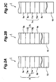
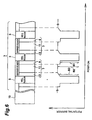
- Fig. 1 is a view showing a semiconductor optical device.
- Figs. 2A, 2B and 2C are views showing the structures of an active region.
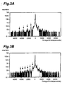
- Fig. 3A is an XRD profile showing the measurement result of the (0002) surface in the quantum well structure having five well layers and barrier layers alternately arranged, the well layers and barrier layers being formed at the same temperature.
- Fig. 3B is an XRD profile showing the measurement result of the (0002) surface in the quantum well structure including five well layers and barrier layers A, B, and C.
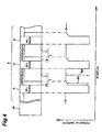
- Fig. 4 is a view showing a potential barrier profile of an active region in a modified semiconductor optical device according to the first embodiment.
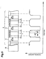
- Fig. 5 is a view showing a potential barrier profile of an active region in a modified semiconductor optical device according to the first embodiment.
- Fig. 6 is a view showing a potential barrier profile of an active region in a modified semiconductor optical device according to the first embodiment.
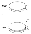
- Fig. 7A and Fig. 7B are views explaining a method of forming a semiconductor device in the second embodiment of the present invention.
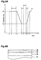
- Fig. 8A is a view showing a temperature profile for forming a well layer and barrier layers.
- Fig. 8B is a view showing a quantum well structure fabricated using the temperature profile P shown in Fig. 8A .
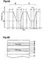
- Fig. 9A is a view showing a temperature profile for forming well layers and barrier layers.
- Fig. 9B is a view showing a quantum well structure fabricated using the temperature profile P shown in Fig. 9A .
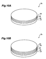
- Fig. 10A and Fig. 10B are views explaining a method of forming a semiconductor device in the second embodiment of the present invention.
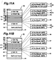
- Fig. 11A is a view showing a light emitting diode according to the second embodiment.
- Fig. 11B is a view showing a light emitting diode having another structure.
- Fig. 12A and Fig. 12B are views showing atomic force microscope (AFM) images in the structures of Fig. 11A and Fig. 11B , respectively.
- AFM atomic force microscope
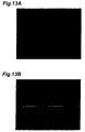
- Fig. 13A is a view showing a fluorescence microscope image of a surface of an epitaxial layer for the light emitting diode shown in Fig. 11A
- Fig. 13B is a view showing a fluorescence microscope image of a surface of an epitaxial layer for the light emitting diode shown in Fig. 11B .
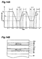
- Fig. 14A is a view showing a temperature profile for a film formation in a method of forming a semiconductor device in the third embodiment according to the present invention.
- Fig. 14B is a view showing a structure of the semiconductor device fabricated by the method shown in Fig. 14A .
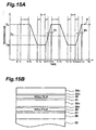
- Fig. 15A is a view showing a temperature profile for a film formation in a modified method of forming the semiconductor device according to the third embodiment.
- Fig. 15B is a view showing a structure of the semiconductor device fabricated by the method shown in Fig. 15A .
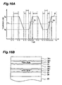
- Fig. 16A is a view showing a temperature profile of a film formation in another modified method of forming the semiconductor device according to the third embodiment.
- Fig. 16B is a view showing a structure of the semiconductor device fabricated by the method shown in Fig. 16A .
- Fig. 17A and Fig. 17B are views showing luminous images of light emitting diodes.
- Fig. 1 is a view showing a semiconductor optical device.
- Fig. 2A to Fig. 2C are views showing some examples of the active region in semiconductor optical device.
- the semiconductor device 1 includes an active region 3 having a quantum well structure.
- the active region 3 includes well regions 5 and barrier region 7.
- the well regions 5 are made of a III-V nitride semiconductor containing nitrogen (N), indium (In) and gallium (Ga).
- the barrier region 7 is made of a III-V nitride semiconductor containing nitrogen (N), indium (In) and gallium (Ga).
- a barrier region 7a has a first semiconductor layer 9a and a second semiconductor layer 11a.
- the first semiconductor layer 9a is made of a III-V compound semiconductor containing at least nitrogen (N), indium (In) and gallium (Ga).
- the second semiconductor layer 11a is made of a III-V compound semiconductor containing at least nitrogen (N) and gallium (N), and may contain indium (In).
- the first semiconductor layer 9a is provided between the second semiconductor layer 11a and a well region 5a.
- the indium composition of the first semiconductor layer 9a is smaller than that of the well regions 5a and 5b. If the second semiconductor layer 11a contains indium, its indium composition is smaller than that of the first semiconductor layer 9a.
- the quantum well structure having an abrupt junction between the well region and the barrier region is formed because the first semiconductor layer 9a and the well region both contain indium and the first semiconductor layer 9a in the first barrier region 7a is provided between the second semiconductor layer 11a and the well region 5a.
- a barrier region 7b has a third semiconductor layer 13b and a second semiconductor layer 11b.
- the third semiconductor layer 13b is made of a III-V compound semiconductor containing at least nitrogen (N), indium (In) and gallium (Ga).
- the second semiconductor layer 11b is made of a III-V compound semiconductor containing at least nitrogen (N) and gallium (Ga), and may further contain indium (In).
- the third semiconductor layer 13b is provided between the second semiconductor layer 11b and a well region 5b. If the second semiconductor layer 11b contains indium, its indium composition is smaller than that of the third semiconductor layer 13b.
- the indium composition of the third semiconductor layer 13b is smaller than that of well regions 5a and 5b.
- the semiconductor device 1 Since the well region 5b and the third semiconductor layer 13b both contain indium and the third semiconductor layer 13b is provided between the second semiconductor layer 11b and the well region 5b, the semiconductor device 1 has a quantum well structure with an abrupt junction between the well region and the barrier region.
- a barrier region 7c has a first semiconductor layer 9c, a second semiconductor layer 11c, and a third semiconductor layer 13c.
- the first semiconductor layer 9c is made of a III-V compound semiconductor containing at least nitrogen (N), indium (In) and gallium (Ga).
- the second semiconductor layer 11c is made of a III-V compound semiconductor containing at least nitrogen (N) and gallium (Ga), and may further contain indium.
- the third semiconductor layer 13c is made of a III-V compound semiconductor containing at least nitrogen (N), indium (In) and gallium (Ga).
- the first semiconductor layer 9c is provided between the second semiconductor layer 11c and the well region 5a.
- the third semiconductor layer 13c is provided between the second semiconductor layer 11c and the well region 5b. If the second semiconductor layer 11c contains indium, its indium composition is smaller than those of the first semiconductor layer 9c and the third semiconductor layer 13c. The indium compositions of the first and third semiconductor layers 9c, 13c are smaller than that of the well regions 5a, 5b.
- This semiconductor device 1 has a quantum well structure with abrupt junctions between the barrier region 7c and the well regions 5a and 5b because the first and third semiconductor layers 9c, 13c and the well regions 5a, 5b contain indium and the first and third semiconductor layers 9c, 13c are provided between the second semiconductor layer 11c and the well regions 5a, 5b, respectively.
- the active region 3 is provided on a primary surface 15a of a support member 15.
- the support member 15 can be, for example, a gallium nitride substrate and the support member 15 may include a gallium nitride substrate and a gallium nitride layer provided thereon.
- the semiconductor optical device 1 may include a first conductivity type semiconductor layer 17 and a second conductivity type semiconductor layer 19.
- the active region 3 is provided between the second conductivity type semiconductor layer 19 and the first conductivity type semiconductor layer 17.
- the semiconductor optical device 1 may include a second conductivity type contact layer 18.
- the second conductivity type semiconductor layer 19 is provided between the second conductivity type contact layer 18 and the active region 3.
- an electrode 20a is provided so as to cover the contact layer 18, and an electrode 20b is provided on a backside 15b of the support member 15.
- the first semiconductor layer 9a (9c) in the active region 3 is provided so as to cover the second semiconductor layer 11a (11c) of the barrier region 7a (7c).
- the well region 5a (5a) is provided on the barrier region 7a (7c).
- the first semiconductor layer 9a (9c) of the composition different from that of the second semiconductor layer 11a (11c) is formed prior to forming the well region 5a (5a). If constituents of the first semiconductor layer 9a (9c) are substantially the same as those of the well region 5a (5a), the first semiconductor layer 9a (9c) can provide a base suitable for forming the well region 5a (5a).
- the barrier region 7b (7c) in the active region 3 is provided on the well region 5b (5b).
- the third semiconductor layer 13b (13c) is provided so as to cover the well region 5b (5b).
- the third semiconductor layer 13b (13c) of the composition different from that of the second semiconductor layer 11b (11c) can be formed prior to forming the second semiconductor layer 11b (11c) of the barrier region 7b (7c).
- the well region 5b (5b) can be protected by use of the third semiconductor layer 13b (13c) during the formation of the second semiconductor layer 11b (11c).
- the second semiconductor layer 11a, 11b, 11c of the respective barrier regions can be made of an In X2 Ga 1-X2 N semiconductor, where X2 is not less than zero and is less than one.
- the first and third semiconductor layers 9a, 9c, 13b, 13c of the respective barrier regions can be made of an In X1 Ga 1-X1 N semiconductor, where X1 is more than zero and less than one.
- the well regions 5a, 5b can be made of an In X3 Ga 1-X3 N semiconductor, where X3 is more than zero and less than one.
- X3 is larger than X2 and X1 is larger than X2 (0 ⁇ X2 ⁇ X1 ⁇ X3).
- the indium composition difference (X3 - X1) between the first and third semiconductor layers 9a, 9c, 13b, 13c made of the In X1 Ga 1-X1 N semiconductor and the well regions 5a, 5b made of the In X3 Ga 1-X3 N semiconductor is not less than 0.04.
- the first and third semiconductor layers function as barrier layers and can confine carriers into the quantum well region.
- (X1 - X2) is preferably not more than 0.02 and the first and third semiconductor layers having compositions in the above range (X1 - X2 ⁇ 0.02) function as barrier region and are effective in confining the carrier into the quantum well region.
- the thickness D of the first and third semiconductor layers 9a, 9c, 13b, 13c is preferably not less than 1 nanometer.
- the well region 5b can be protected during the formation of the second semiconductor layer 11a, 11c, and the first semiconductor layers 9a, 9c with a surface suitable for formation of the well region 5a can be formed on the second semiconductor layer 11a, 11c.
- the first and third semiconductor layers 9a, 9c, 13b, 13c have respective thickness values not more than 5 nanometers.
- the second semiconductor layer 11a, 11b, 11c have respective thickness values sufficient to improve the crystal quality of the barrier region.
- the thickness of the barrier region is preferably not less than 5 nanometers. Within this thickness range, at least two semiconductor layers can be formed. The thickness of the barrier region is preferably not more than 30 nanometers. The thickness over this range increases driving voltage for the semiconductor device and thus may shorten the lifetime thereof.
- This light emitting diode has the following structure:
- Figs. 4 , 5 , and 6 are illustrations showing potential barriers of the active region in some modified semiconductor optical devices.
- a third semiconductor layer 13 is located between a second semiconductor layer 11 in the barrier region 7 and the well region 5.
- a relatively large potential barrier is formed between the third semiconductor layer 13 and the well region 5.
- the potential barrier monotonically changes in the third semiconductor layer 13 between the well region 5 and the second semiconductor layer 11.
- the well region 5, third semiconductor layer 13 and second semiconductor layer 11 are periodically arranged to form the active region 3.
- the barrier region has a number of semiconductor layers each having a different composition from each other and thus improves the periodicity of the active region 3.
- the potential barrier B2 of the second semiconductor layer 11 is larger than the potential barrier B3 of the third semiconductor layer 13.
- the third semiconductor layer 13 is located between the second semiconductor layer 11 of the barrier region 7 and the well region 5, and a first semiconductor layer 9 is located between the second semiconductor layer 11 and another well region 5.
- Relatively large potential barriers are formed in the following arrangements: between the third semiconductor layers 13 and the well region 5; between the first semiconductor layers 9 and the other well region 5.
- the potential barriers monotonically change in the first semiconductor layer 9 between the well region 5 and the second semiconductor layer 11 and in the third semiconductor layers 13 between the other well region 5 and the second semiconductor layer 11.
- the well region 5, first semiconductor layer 9, second semiconductor layer 11 and third semiconductor layer 13 are periodically arranged to form the active region 3.
- the barrier region has a number of semiconductor layers each having a composition different from each other and thus improves the periodicity of the active region 3.
- the potential barrier B2 of the second semiconductor layer 11 is larger than the potential barrier B1 of the first semiconductor layer 9.
- the potential barrier B2 of the second semiconductor layer 11 is also larger than the potential barrier B3 of the third semiconductor layer 13.
- the third semiconductor layer 13 is provided between the well region 5 and the second semiconductor layer 11 of the barrier region 7, and the first semiconductor layer 9 is located between the second semiconductor layer 11 and another well region 5.
- Large potential barriers are formed in the following arrangement: between the third semiconductor layer 13 and the well region 5; between the first semiconductor layer 9 and the other well regions 5.
- the potential barrier monotonically changes in the third semiconductor layer 13 between the well region and the second semiconductor layer 11.
- the potential barrier is almost constant in the first semiconductor layer 9 between the well region 5 and the second semiconductor layer 11.
- the well region 5, first semiconductor layer 9, second semiconductor layer 11 and third semiconductor layer 13 are periodically arranged to form the active region 3.
- the barrier region has a number of semiconductor layers each having a composition different from each other and thus improves the periodicity of the active region 3.
- the potential barrier B2 of the second semiconductor layer 11 is larger than the potential barrier B1 of the first semiconductor layer 9.
- the potential barrier B2 of the second semiconductor layer 11 is larger than the potential barrier B3 of the third semiconductor layer 13.
- the abrupt interfaces are formed between the well regions and the barrier regions in the quantum well structure.
- FIG. 7A and Fig. 7B are illustrations explaining a method of forming a semiconductor device as shown as the second embodiment of the present invention.
- a substrate is prepared.
- the substrate can be, for example, a single-crystal wafer made of gallium nitride.
- a gallium nitride film may be grown on this wafer, if required.
- organometallic vapor phase epitaxy (OMVPE) can be used to form this gallium nitride film and other III-V nitride semiconductor films formed in subsequent production steps.
- OMVPE organometallic vapor phase epitaxy
- a III-V nitride semiconductor film such as a gallium nitride layer 23, is grown on the gallium nitride substrate 21.
- the gallium nitride film 23 has an n type conductivity.
- the gallium nitride film 23 can work as a cladding layer, for example.
- an active region 25 is grown on the gallium nitride layer 23 to form a semiconductor substrate product E 1 like an epitaxial wafer.
- the active region 25 has a quantum well structure including well films and barrier semiconductor films.
- Fig. 8A is a diagram showing a temperature profile for forming a well film and barrier semiconductor films.
- Fig. 8B is an illustration showing a quantum well structure fabricated by use of the temperature profile P shown in Fig. 8A .
- a barrier A film 26, a barrier B film 27, a well film 28 and a barrier C film 29 are grown on the gallium nitride layer 23. As shown in Fig.
- the barrier A film 26 is formed at the temperature T B using a source gas therefor.
- the barrier A film 26 can be, for example, a III-V nitride semiconductor film, such as an undoped GaN film or an undoped InGaN film.
- the barrier A film 26 is grown in a period from time t 1 to time t 2 .
- the supply of the source gas is terminated to complete the formation of the barrier A film 26.
- change of the temperature starts.
- the temperature is T W .
- the barrier B film 27 is grown using a source gas therefor. In a period from time t 4 to time t 5 , the barrier B film 27 is formed prior to forming the well film 28.
- the barrier B film 27 is made of a III-V nitride semiconductor containing at least nitrogen (N), indium (In) and gallium (Ga), for example, an undoped InGaN film. A part or the whole of the barrier B film 27 may be formed at the temperature T W . In a preferred example, the barrier B film 27 is grown at the temperature T W .
- the OMVPE apparatus is set at the preferred temperature T W for formation of the well film (e.g., 820 degrees Celsius) and the source gas for the barrier B film 27 is changed to the source gas for the well film 28.
- the well film 28 is formed at the temperature T W .
- the well film 28 is made of a III-V nitride semiconductor containing at least nitrogen, indium and gallium.
- the step of forming the well film 28 is performed continuously after the step of forming the barrier B film 27, so that the well layer 28 is grown substantially in succession to the barrier B film 27.
- This method includes the step of changing the temperature without the formation of a semiconductor film after the step of forming the barrier A film 26.
- the barrier B film 27 is grown on the barrier A film 26 prior to the formation of the well film 28. Accordingly, an abrupt interface is provided between the well film 28 and the barrier B film 27.
- the barrier A film 26 is grown at the temperature T B higher than the temperature T W .
- a part or the whole of the barrier B film 27 is grown at the temperature T W .
- the indium composition of the barrier B film 27 is smaller than that of the well film 28.
- the barrier A film 26, the barrier B film 27 and the well film 28 can be, for example, an undoped GaN film, an undoped In 0.01 Ga 0.99 N film and an undoped In 0.15 Ga 0.85 N film, respectively.
- the OMVPE apparatus is set at the temperature T W , e.g., 820 degrees Celsius, suitable for the formation of the well film.
- a source gas for the barrier C film is then supplied at time t 6 to grow the barrier C film 29 on the well film 28.
- the source gas for the well film is changed to supply the source gas for the barrier C film.
- the barrier C film 29 is made of a III-V nitride semiconductor containing nitrogen, gallium and indium. The formation of the barrier C film 29 is started at the temperature Tw.
- the temperature starts to change.
- the supply of the source gas for the barrier C film is terminated.
- the barrier C film 29 is grown.
- the step of changing the temperature without forming a film is provided between time t 8 and time t 9 .
- the OMVPE apparatus is set at the temperature of T B .
- the barrier C film 29 is formed at the temperature that is lower than the temperature T B and is not lower than the temperature T W , and the indium composition of the barrier C film 29 is smaller than that of the well film 28.
- the barrier C film 29 can be, for example, an undoped In 0.01 Ga 0.99 N film.
- This method has the step of forming the barrier C film 29 which is performed prior to the step of changing the temperature without forming a film and after the formation of the well film 28. Accordingly, the junction between the well film 28 and the barrier C film becomes abrupt.
- Fig. 9A is a diagram showing a temperature profile for the formation of well films and barrier films.
- Fig. 9B is an illustration showing the quantum well structure fabricated by use of the temperature profile P shown in Fig. 9A .
- a barrier A film 30, a barrier B film 31, a well film 32 and a barrier C film 33 are further formed on the barrier C film 29.
- the sequence S1 shown in Fig. 9A is prepared, and this sequence is repeated by a number of times until the desired active region is formed.
- the sequence S1 is substantially the same as sequence S0 and time t 1 to t 9 in the sequence S0 correspond to time t 10 to t 18 in the sequence S0.
- a barrier A film 34 is formed on the barrier C film 33 in a period from time t 19 to time t 20 . Then, the formation of the active region 25 is completed.
- Fig. 10A and Fig. 10B are illustrations explaining a method of forming a semiconductor device in the second embodiment of the present invention.
- a III-V nitride film 35 containing at least nitrogen (N), aluminum (Al) and gallium (Ga) is formed on the active region 25 to provide a semiconductor substrate product E 2 such as an epitaxial wafer.
- the III-V nitride film 35 has the p type conductivity.
- the III-V nitride semiconductor film 35 is used as a cladding layer and is made of an AlGaN semiconductor, for example. Then, as shown in Fig.
- a III-V nitride semiconductor film 37 containing at least nitrogen and gallium is formed on the III-V nitride semiconductor film 35 to provide a semiconductor substrate product E 3 such as an epitaxial wafer.
- the III-V nitride semiconductor film 37 has the p type conductivity.
- the III-V nitride semiconductor film 37 is used as a contact layer and is made of GaN semiconductor, for example.
- the present embodiment describes the formation of the barrier region having the barrier A film, the barrier B film and the barrier C film
- a person skilled in the art can form another barrier region based on the description of the present embodiment, such as the barrier region having the barrier A film and the barrier B film or to form the barrier region having the barrier A film and the barrier C film.
- the barrier B film and the barrier C film are made of the III-V nitride without aluminum, the bandgap of the barrier B film and the barrier C film is not larger than the bandgap of the barrier A film.
- the crystal quality of the barrier B film and the barrier C film is better than that of the AlGaN film grown at about 800 degrees Celsius and strain to the well film becomes small. Since the barrier B film is located under the well film, the well film does not touch the surface of the barrier A film which may be contaminated during the temperature change from the film formation temperature of the barrier A film to the growth temperature of the well film.
- the barrier C film prevents the decomposition of indium atoms from the well film during the temperature change from the temperature for formation of the well film to the temperature for growth of the barrier A film. Since the barrier B film and the barrier C film have indium compositions smaller than that of the well film, the cover of the barrier C film prevents the decomposition of indium atoms from the well film during the change of temperature of the film forming apparatus. Accordingly, good quality of the well layer is obtained. Since the barrier B film and the barrier C film that are thinner than the barrier A film are provided between the well film and the barrier A film, the barrier A film with good crystal quality can be formed at high temperatures.
- the barrier A film such as the gallium nitride layer can be grown by step-flow using carrier gas H 2 .
- the growth temperature of the barrier A film is not lower than 900 degrees Celsius.
- the growth temperature of the barrier A film is preferably not higher than 1200 degrees Celsius. Accordingly, the crystal quality and flatness of the barrier semiconductor film be improved.
- the growth temperature of the well film depends on the desired indium composition thereof and is preferably not lower than 600 degrees Celsius and not higher than 900°C.
- a part or the whole of the barrier B film and the barrier C film can be grown during the temperature change. This growth manner can reduce time period necessary for formation of the active region. This results in shortening the duration in which the well region is placed under temperatures higher than the temperature of forming itself.
- a quantum well structure includes the well layers of InGaN and the barrier layers of GaN (or InGaN), the well layers are formed at the same temperature and in the same atmosphere as the barrier layers.
- the optimal deposition temperature for the barrier layers is higher than the optimal deposition temperature for the well layers.
- the crystal quality of the barrier layers is improved.
- the constituents of the well layers are decomposed therefrom and one of constituents, e.g., indium, desorbs from the surface thereof. This desorption makes it difficult to obtain a quantum well structure with excellent abrupt interfaces, and if the barrier layers are formed at a low temperature, crystal defects is likely to occur therein.
- the additional barrier semiconductor film is formed prior to the growth of a well film, and thus improves the crystal quality of the well film. Since the additional barrier semiconductor film is formed after growth of the well film, the crystal quality of the well film and the abruptness of the interface between the well film and the barrier film are not deteriorated and the crystal quality of the barrier semiconductor films is improved.
- Figs 3A and 3B are views of XRD profiles for evaluation and Fig 3B shows higher-order satellite peaks than Fig 3A .
- the semiconductor light generating device, such as the light emitting diode, formed by this method demonstrates good emission characteristics.
- Fig. 11A is an illustration showing a light emitting diode according to the present embodiment. Fabrication of the light emitting diode 51 will be described.
- a pretreatment (thermal cleaning) for GaN substrate 53 is carried out at about 1050 degrees Celsius in an atmosphere containing ammonia (NH 3 ) and hydrogen (H 2 ) for about ten minutes. After this pretreatment, a GaN semiconductor is grown at 1150 degrees Celsius on the GaN substrate 53 while being doped with silicon to obtain, for example, an n-type GaN film 55 of 2 micrometer thick.
- NH 3 ammonia
- H 2 hydrogen
- an InGaN semiconductor is grown at the temperature of 900 degrees Celsius to obtain, for example, an undoped (hereinafter abbreviated to "ud") In 0.01 Ga 0.99 N film 57 of 15 nanometer thick. Thereafter the temperature is changed.
- An InGaN semiconductor is grown at 820 degrees Celsius to obtain, for example, an ud-In 0.015 Ga 0.985 N film 59 of 3 nanometer thick.
- the ud-In 0.01 Ga 0.99 N film 57 and ud-In 0.015 Ga 0.985 N film 59 function as a lower cladding layer 61.
- an InGaN semiconductor is grown at the temperature of 820 degrees Celsius to obtain, for example, an ud-In 0.15 Ga 0.85 N film 65 of 2.5 nanometer thick.
- the ud-In 0.15 Ga 0.85 N film 65 functions as a well region.
- the temperature is changed from 820 to 900 degrees Celsius.
- an InGaN semiconductor is grown to obtain, for example, an ud-In U Ga 1-U N film 67 of 3 nanometer thick.
- the indium composition of the semiconductor film 67 decreases with distance from the well film.
- the ud-In U Ga 1-U N film 67 constitutes a part of a barrier region 73.
- a gas flow rate to form an In 0.015 Ga 0.985 N film at 820 degrees Celsius is used.
- an InGaN semiconductor is grown at the temperature to obtain, for example, an ud-In 0.01 Ga 0.99 N film 69 of 12 nanometer thick.
- the ud-In 0.01 Ga 0.99 N film 69 constitutes a part of the barrier region 73.
- the temperature is changed from 900 to 820 degrees Celsius. After the temperature becomes stable at 820 degrees Celsius, an InGaN semiconductor is grown at the temperature to obtain, for example, an ud-In 0.015 Ga 0.985 N film 71 of 3 nanometer thick.
- the ud-In 0.015 Ga 0.985 N film 71 constitutes a part of the barrier region 73.
- an upper cladding layer 63 is grown.
- the temperature is changed from 820 to 900 degrees Celsius.
- an InGaN semiconductor is grown to obtain, for example, an ud-In V Ga 1-V N film 72 of 3 nanometer thick.
- the indium composition of this semiconductor film 72 decreases with distance from the well film.
- the ud-In V Ga 1-V N film 72 constitutes a part of the upper cladding layer 63.
- a gas flow rate to form an In 0.015 Ga 0.985 N film at 820 degrees Celsius is used.
- an InGaN semiconductor is grown at the temperature to obtain, for example, an ud-In 0.01 Ga 0.99 N film 75 of 15 nanometer thick.
- the ud-In 0.01 Ga 0.99 N film 75 constitutes a part of the upper cladding layer 63.
- an Mg-doped AlGaN semiconductor is grown at the temperature of 1100 degrees Celsius to obtain, for example, a p-type Al 0.15 Ga 0.85 N film 77 of 20 nanometer thick.
- the p-type Al 0.15 Ga 0.85 N film 77 functions as a second cladding layer.
- an Mg-doped GaN semiconductor is grown to obtain, for example, a p-type GaN film 79 of 50 nanometer thick.
- the p-type GaN film 79 functions as a contact layer.
- a cathode electrode 81 made of Ti/Al is formed on a back surface of the substrate 53, and a semi-transparent electrode 83 made of Ni/Au is formed on the contact layer.
- a pad electrode 85 made of Ti/Au is formed on the semitransparent electrode 83.
- Fig. 11B is an illustration showing a light emitting diode having another structure. Fabrication of the light emitting diode 91 will be described. In the case of the light emitting diode 91, particularly, a lower cladding layer 93, well regions 95, barrier regions 97, and an upper cladding layer 99 are formed at the same temperature, e.g., at 820 degrees Celsius.
- Fig. 12A and Fig. 12B are illustrations showing atomic force microscope (AFM) images in the structures of Fig. 11A and Fig. 11B , respectively.
- AFM photographs show images of the surface of the quantum well structure (in the area of 10 ⁇ m ⁇ 10 ⁇ m) without growth of the p-AlGaN layer and p-GaN layer.
- the AFM image shown in Fig. 12B corresponds to the light emitting diode with the well layers and barrier layers formed at the same temperature, and shows four defects resulting from indium segregation.
- the defect density is preferably not more than 1 ⁇ 10 6 per square centimeter (1 ⁇ 10 6 cm -2 ).
- the defects appearing in Fig. 12B result from In segregation and are likely to appear at the relatively low temperature for depositing InGaN, where the In composition of InGaN is relatively high, where molar ratio [mole concentration of V group gas]/[mole concentration of III group gas] is relatively low in the growth of InGaN, and so on.
- Fig. 13A is a view of a fluorescence microscope image showing the surface of an epitaxial layer for the light emitting diode shown in Fig. 11A
- Fig. 13B a view of a fluorescence microscope image showing the surface of an epitaxial layer for the light emitting diode shown in Fig. 11B .
- the crystal quality of the barrier film is excellent because the barrier region is formed at the temperature different from that of the well region.
- the light emitting diode 51 emits light of almost uniform intensity.
- the crystal quality of the barrier film is not so good because the barrier region is formed at the same temperature as the well region.
- the film quality of the well region is nonuniform and the light emitting diode 91 has some non-luminous regions.
- the optical power of the light emitting diode 51 is 2.5 times the optical power of the light emitting diode 91.
- Fig. 14A and Fig. 14B are illustrations explaining a method of forming a semiconductor device in the third embodiment of the present invention. This method is different in the following points from the embodiment shown in Fig. 9A and Fig. 9B : the temperature is increased in a period from time t 7 to t 9 , the temperature is maintained at T B in a period M 1 between time t 9 and t 21 (instead of time t 10 ), and a barrier A film 30a is formed in a period from time t 21 to t 11 .
- the temperature is increased in a period from time t 16 to t 18 , the temperature is maintained at T 8 in a period M 1 from time t 18 to t 22 (instead of time t 19 ), and a barrier A film 34a is formed in a period between time t 22 and t 20 .
- the step of maintaining the temperature T B in the period M 1 without forming a semiconductor film is provided after the previous barrier formation.
- atoms from the formed barrier film can migrate thereon at the temperature T B higher than both the film formation temperature of the well film and the temperature during the temperature rise. This results in improving the flatness of the surface of the barrier film and the crystal quality of the active region previously formed and can provide a base suitable for forming the subsequent barrier film.
- Fig. 15A and Fig. 15B are illustrations explaining a modified method of forming the semiconductor device in the third embodiment of the present invention. This method is different in the following points from the embodiment shown in Fig. 9A and Fig. 9B : the temperature is increased in a period from time t 7 to t 24 , and a barrier C film 29b is formed in a period from time t 6 to t 23 (instead of time t 8 ). The temperature is increased without forming a film in a period M 2 from time t 23 to t 24 and, a barrier A film 30b is formed in a period from time t 25 (instead of time t 10 ) to t 11 after the temperature becomes stable.
- the temperature is increased in a period from time t 16 to time t 27 and a barrier C film 33b is formed in a period from time t 15 to time t 26 (instead of time t 17 ).
- the temperature is increased without forming a film in a period M 2 from time t 26 to time t 27 and, a barrier A film 34b is formed in a period from time t 28 (instead of time t 19 ) to time t 20 after the temperature becomes stable.
- the step of changing the temperature without forming a semiconductor film is provided after the previous barrier formation.
- This step permits atoms from the formed barrier film to migrate thereon. This results in improving the flatness of the surface of the barrier film and the crystal quality of the active region as compared to conventional devices, and can provide a base surface suitable for the subsequent barrier film formation.
- Fig. 16A and Fig. 16B are illustrations explaining a modified method of forming the semiconductor device in the third embodiment of the present invention. This method is different in the following points from the embodiment shown in Fig. 9A and Fig. 9B : a barrier C film 29c is formed in a period from time t 6 to t 29 (instead of time t 8 ); the temperature is increased without forming a semiconductor film in a period from time t 29 to t 30 ; the temperature is maintained at T B in a period from time t 30 to t 31 . After the temperature becomes stable, a barrier A film 30c is formed in a period from time t 31 (instead of time t 10 ) to t 11 .
- a barrier C film 33c is formed in a period from time t 15 to t 32 (instead of time t 17 ), the temperature is increased without forming a film in a period from time t 32 to time t 33 , and the temperature is maintained at T B in a period from time t 33 to t 34 .
- a barrier A film 34c is formed in a period from time t 34 (instead of time t 19 ) to t 20 .
- the step of changing the temperature without forming a semiconductor film and the step of maintaining the temperature is provided. These steps permit atoms from the formed barrier film to migrate thereon. This results in improving the flatness of the surface of the barrier film and the crystal quality of the active region and can provide a base surface suitable for the subsequent barrier film formation.
- any film formation is not carried out in the periods M 1 (e.g., the period from time t 9 to t 21 ), M 2 and M 3 to provide the previously grown semiconductor films with the thermal treatment in these examples and modifications.
- These periods enables atoms from the third barrier film to migrate thereon.
- the periods M 1 , M 2 and M 3 are preferably not less than one minute nor more than five minutes. In this method, sufficient migration will not occur if the period of increasing the temperature without forming a semiconductor film or the period of maintaining the temperature without forming a semiconductor film is too short. If these periods are too long, the emission characteristics of the light emitting device are not improved because of the contamination of the growing surface and/or degradation of crystal quality of the active layer.
- Fig. 17A and Fig. 17B are views showing emission images of light emitting diodes.
- the structure of these light emitting diodes is substantially the same as the structure shown in Fig. 11A .
- fabrication of the light emitting diode shown in Fig. 17A after the InGaN layers 67 and 72 are grown with change of temperature in the period of 30 seconds, two minutes are prepared for the temperature rise period to 900 degrees Celsius and the temperature maintaining period for stabilization.
- the first barrier layer is grown with a temperature rise to 900 degrees Celsius in a period of 2.5 minutes immediately after the formation of the well films 65, 71, and thus "period of changing temperature without forming a film" is not provided unlike the fabrication of the light emitting diode shown in Fig. 17A .
- the first barrier layer is formed in the same thickness by controlling the growth rate.
- the light emitting device exhibits uniform intensity of light
- Fig. 17B luminescent spots are observed in the luminous surface.
- the occurrence of these luminescent spots results from the crystal quality of each barrier layer formed with a temperature rise. It is thought that the barrier layer has a region with a poor crystal quality which is formed near the well layer and is not recovered with the growth thereof and that the poor crystal quality adversely affects the growth of the next well layer. Since the well layers are made of InGaN with high In composition, the quality thereof is likely to deteriorate if the crystal quality of the base surface is not good.
- the migration of atoms occurs in the vicinity of the surface of the first barrier film in the period of changing the temperature without forming a semiconductor film, thereby achieving good crystal quality and flatness of the first barrier film. That is, the crystal quality of the active layer can be recovered by providing the foregoing intermission of growth, in addition to the growth of the barrier at the temperature higher than that of the well layer, so that the quality of the active layer can be further enhanced.
- the first barrier layer is grown with increasing temperature and the second barrier layer is grown after the temperature becomes constant at a high temperature.
- the growth conditions are changed for formation of the second barrier layer so as to increase the growth rate and the partial pressure of hydrogen (H 2 ), and decrease the V/III molar ratio.
- the first barrier layer is grown with increasing temperature by the method in Document 4, and the first and the second barrier layers are continuously formed.
- the crystal quality of the first barrier layer is gradually improved in this method as the first barrier layer grows, the first barrier layer has a region near the well layer the crystal quality of which is insufficient.
- the embodiments according to the present invention describe semiconductor optical device, such as a light emitting diode, but the present invention is not limited to the quantum well structures for the light emitting layers.
- the present invention can also be used for other semiconductor devices having the quantum well structure, besides the semiconductor light emitting devices. Details of structures of these devices can be modified as necessary. We therefore claim all modifications and variations coming within the scope of the following claims.
Landscapes
- Physics & Mathematics (AREA)
- Nanotechnology (AREA)
- Engineering & Computer Science (AREA)
- Chemical & Material Sciences (AREA)
- Optics & Photonics (AREA)
- Biophysics (AREA)
- Life Sciences & Earth Sciences (AREA)
- Electromagnetism (AREA)
- General Physics & Mathematics (AREA)
- Crystallography & Structural Chemistry (AREA)
- Condensed Matter Physics & Semiconductors (AREA)
- Led Devices (AREA)
- Semiconductor Lasers (AREA)
- Recrystallisation Techniques (AREA)
- Physical Deposition Of Substances That Are Components Of Semiconductor Devices (AREA)
Description
- The present invention relates to a semiconductor device having a quantum well structure and to a method of forming the same.
- Document 1 (
Japanese Patent Application Laid-Open No. 2001-168471 - Document 2 (
Japanese Patent Application Laid-Open No. 10-84132 - Document 3 (
Japanese Patent Application Laid-Open No. 6-268257 - Document 4 (
Japanese Patent Application Laid-Open No. 2002-43618 -
EP 1 248 303 A - In the semiconductor light emitting device disclosed in
Document 1, the semiconductor layer referred to as the intermediate layers is formed of AlGaN semiconductor the bandgap of which is larger than that of the barrier layers. After this AlGaN semiconductor layer (intermediate layer) has been formed on an InGaN semiconductor layer (well layer), the temperature is raised to a temperature for growing the barrier layer and indium atoms are decomposed from the well layer during this raising. This decomposition makes it difficult to form abrupt junctions in the quantum well structure. - In the semiconductor light emitting device disclosed in
Document 2, the semiconductor layer referred to as the buffer layers is grown so as not to work as a substantial barrier layer. Since the lattice constant of the buffer layers is between that of the quantum well layers and that of the barrier layers, the buffer layers alleviate stress from the difference between the lattice constants of the barrier layer and the quantum well layer. But, a relatively large potential barrier is formed at respective interfaces in the following arrangements: between the quantum well layers and the buffer layers; between the buffer layers and the barrier layers. The quantum well structure increases the number of interfaces exhibiting the relatively large potential barrier because of the following: the lattice constant of the buffer layers is selected around the midpoint between that of the barrier layers and that of the well layer; the buffer layers and the well layer therebetween are inevitably located between the barrier layers. - In the semiconductor light emitting device disclosed in
Document 3, the light generating region is formed by repetitively growing the InGaN layers of different compositions at 800 degrees Celsius. With increase of the number of growth of the InGaN layers, flatness of the surfaces of the InGaN layers is degraded growth by growth and thus it is difficult to form abrupt junctions between the InGaN layers. What is needed in single or multiple quantum well structures is abrupt junctions between well layers and barrier layers therein. - It is an object of the present invention to provide a semiconductor device providing an abrupt junction in the quantum well structure, and a method of forming the semiconductor device.
- One aspect of the present invention relates to a method as defined in
claim 1 of forming a semiconductor device having a quantum well structure. - This method has the period of changing the temperature without depositing any semiconductor film after the first barrier film has been formed on the well film. Thus, the second barrier film is formed on the first barrier film at the second temperature after the well film is covered with the first barrier film. The method provides a abrupt junction between the well film and the barrier film and improves the flatness of the quantum well structure.
- In an embodiment of the method of the present invention, in the step of forming the first barrier film on the well film, at least a portion of the first barrier film is grown while changing a growth temperature.
- In this method, a portion of the first barrier film is formed while raising the temperature from the first temperature to the second temperature, which can gradually improve the crystal quality of the first barrier film and can also reduce damage to the well film during the temperature change.
- Another embodiment of the present invention relates to a method of forming a semiconductor device having a quantum well structure. This method comprises the steps of: forming a well film at a first temperature, the well film being made of a III-V nitride semiconductor containing nitrogen, indium and gallium; forming a first barrier film on the well film, the first barrier film being made of a III-V nitride semiconductor containing nitrogen, indium, and gallium, an indium composition of the first barrier film being smaller than an indium composition of the well film; after forming the first barrier film, rising a temperature without depositing a semiconductor film; and forming a second barrier film on the first barrier film at a second temperature, the second barrier film being made of a III-V nitride semiconductor, at least a portion of the first barrier film being formed during a temperature rise from the first temperature to a third temperature, the temperature in the temperature rising step being increased from the third temperature to the second temperature in a predetermined period of time, and a period of time for the temperature rise from the first temperature to the third temperature being shorter than the predetermined period of time.
- After the first barrier film has been formed, the first barrier film is thermally treated during the period of time for rising the temperature to the second temperature without depositing any semiconductor film. Atoms from the first barrier film migrate thereon during the temperature rising step and this migration improves the crystal quality of the active region and provides a semiconductor surface suitable for forming the second barrier film.
- Another embodiment of the present invention relates to a method of forming a semiconductor device having a quantum well structure. This method comprises the steps of: forming a well film at a first temperature, the well film being made of a III-V nitride semiconductor containing nitrogen, indium and gallium; forming a first barrier film on the well film, the first barrier film being made of a III-V nitride semiconductor containing nitrogen, indium and gallium, and an indium composition of the first barrier film being smaller than an indium composition of the well film; after forming the first barrier film, rising a temperature to a second temperature without depositing a semiconductor film; prior to forming a second barrier film, maintaining the second temperature in a predetermined period of time without depositing a semiconductor film; and forming the second barrier film on the first barrier film at the second temperature, the second barrier film being made of a III-V nitride semiconductor, at least a portion of the first barrier film being formed in a period of temperature rise from the first temperature to a third temperature lower than the second temperature, the temperature in the step of rising the temperature being increased from the third temperature to the second temperature, and a period of time for the temperature rise from the first temperature to the third temperature being shorter than the predetermined period of time.
- Prior to the formation of the second barrier film, the first barrier film is thermally treated in the period of time for which the temperature is kept at the second temperature without depositing any semiconductor film. Atoms from the first barrier film migrate thereon during the temperature keeping step and this migration improves the crystal quality of the active region and provides a semiconductor surface suitable for the formation of the second barrier film.
- In an embodiment of the method according to the present invention, the predetermined period is not less than one minute nor more than five minutes. If the period of time for rising the temperature without depositing any semiconductor film and the period of time for which the temperature is kept constant without depositing any semiconductor film is too short, sufficient migration does not occur. If these periods are too long, the emission characteristics of the light emitting device is not improved because of contaminations on the growing surface and/or degradation of crystal quality of the active layer.
- In an embodiment of the method of the present invention, the step of forming the first barrier film on the well film is carried out in direct succession of the step of forming the well film at the first temperature.
- Since the step of forming the first barrier film and the step of forming the well film are carried out without any substantial process steps therebetween, the above method can avoid contaminations on a semiconductor surface which will be the interface between the well film and the first barrier film and can effectively reduce deterioration of the well film in the subsequent temperature rise step.
- In an embodiment of the method of the present invention, the first barrier film includes an InX1Ga1-X1N semiconductor, where X1 is more than zero and less than one, the second barrier film includes an InX2Ga1-X2N semiconductor, where X2 is not less than zero and is less than one, and the well film includes an InX3Ga1-X3N semiconductor, where X3 is more than zero and less than one, and X3 is larger than X1.
- This method provides an abrupt junction between the well film of the InX3Ga1-X3N semiconductor and the first barrier film of the InX1Ga1-X1N semiconductor.
- Another aspect of the present invention relates to a method as defined in claim 8 of forming a semiconductor device having a quantum well structure.
- This method provides the period for changing the temperature without depositing any semiconductor film after the first barrier film has been formed. The second barrier film is formed on the first barrier film after the temperature has been changed, and thus the first barrier film is covered with the second barrier film prior to the formation of the well film. Accordingly, the junction between the well film and the barrier film becomes abrupt.
- In an embodiment of this method of the present invention, in the step of forming the second barrier film on the first barrier film, at least a portion of the second barrier film is formed at the first temperature.
- This method can reduce the period of time necessary for changing the temperature because a portion of the second barrier film is formed at the first temperature and the remaining of the second barrier film is grown in a period of time for stabilizing the temperature prior to forming the well film.
- In an embodiment of this method of the present invention, the step of forming the well film on the second barrier film at the first temperature is carried out in direct succession of the step of forming the second barrier film on the first barrier film.
- In this method, the steps of forming the well film and forming the second barrier film are continuously carried out without any process step therebetween.
- Thus, this method can prevent the contamination on the surface which will be the interface between the well film and the first barrier film.
- In an embodiment of this method of the present invention, the first barrier film is made of an InX2Ga1-X2N semiconductor, where X2 is not less than zero and is less than one. The second barrier film is made of an InX1Ga1-X1N semiconductor, where X1 is more than zero and less than one. The well film is made of an InX3Ga1-X3N semiconductor, where X3 is more than zero and less than one, and X3 is larger than X1.
- This method provides an abrupt junction between the well film of the InX3Ga1-X3N semiconductor and the second barrier film of the InX1Ga1-X1N semiconductor.
- An embodiment of this method of the present invention further comprises: forming a third barrier film on the well film, the third barrier film being made of a III-V nitride semiconductor containing nitrogen, indium and gallium, and an indium composition of the third barrier film being smaller than the indium composition of the well film; after forming the third barrier film, changing temperature without depositing a semiconductor film; and after the step of changing the temperature, forming a fourth barrier film on the third barrier film at a second temperature, the third barrier film being formed at a fourth temperature, the fourth temperature being lower than the second temperature and the fourth temperature being equal to or higher than the first temperature.
- In this method, the period for changing the temperature without depositing any semiconductor film is provided after the third barrier film has been formed on the well film. The well film is covered with the third barrier film before the fourth barrier film is formed on the third barrier film at the second temperature. Accordingly, the junction between the well film and the barrier film exhibits excellent abruptness.
- In this method of the present invention, in the step of forming the third barrier film on the well film, at least a portion of the third barrier film is grown while changing a growth temperature.
- In this method, a part or the whole of the third barrier film is formed while increasing the temperature and thus the crystal quality of the third barrier film can be gradually improved with depositing the film and the damage to the well film during the temperature change can also be reduced.
- An embodiment of this method comprises the steps of: forming a third barrier film on the well film, the third barrier film being made of a III-V nitride semiconductor containing nitrogen, indium and gallium, and an indium composition of the third barrier film being smaller than the indium composition of the well film; after forming the third barrier film, rising a temperature without depositing a semiconductor film; and forming a fourth barrier film on the third barrier film at the second temperature, the fourth barrier film being made of a III-V nitride semiconductor, at least a portion of the third barrier film being formed during the temperature rise from the first temperature to a fourth temperature, the fourth temperature being lower than the second temperature, the temperature in the step of increasing the temperature being increased from the fourth temperature to the second temperature in a predetermined period of time, and a period of time for the temperature rise from the first temperature to the fourth temperature being shorter than the predetermined period of time.
- After the third barrier film has been formed, the third barrier film is thermally treated while rising the temperature to the second temperature without depositing any semiconductor film. Atoms from the third barrier film migrate thereon during the temperature rise. This results in improving the crystal quality of the active region and providing a semiconductor surface suitable for the formation of the fourth barrier film.
- An embodiment of this method comprises the steps of: forming a third barrier film on the well film, the third barrier film being made of a III-V nitride semiconductor containing nitrogen, indium and gallium; after forming the third barrier film, rising a temperature to the second temperature without depositing a semiconductor film; after rising the temperature to the second temperature, maintaining the second temperature in a predetermined period of time without depositing a semiconductor film; and forming a fourth barrier film at the second temperature, the fourth barrier film being made of a III-V nitride semiconductor, at least a portion of the third barrier film being formed in a period of time for the temperature rise from the first temperature to a fourth temperature lower than the second temperature, the temperature in the step of increasing the temperature being increased from the fourth temperature to the second temperature, and a period of time for the temperature rise from the first temperature to the fourth temperature being shorter than the predetermined period of time.
- The third barrier film is thermally treated prior to the formation of the fourth barrier film in the period of time for keeping the temperature at the second temperature without depositing any semiconductor film. Atoms from the third barrier film migrate thereon in the above period. This results in improving the crystal quality of the active region and providing a semiconductor surface suitable for the formation of the fourth barrier film.
- In an embodiment of this method according to the present invention, the predetermined period of time is not less than 1 minute nor more than 5 minutes. In this method, sufficient migration does not occur if the period of time for increasing the temperature without depositing any semiconductor film and the period of time for which the temperature is kept constant without depositing any semiconductor film is too short. If these periods are too long, the emission characteristics of the light emitting device cannot be improved because of the contamination on the growing surface and/or degradation of crystal quality of the active layer.
- In an embodiment of this method of the present invention, the step of forming the third barrier film on the well film is carried out in a succession of the step of forming the well film on the second barrier film at the first temperature.
- Since the steps of forming the third barrier film and forming the well film is continuously carried out, this method can prevent contamination on a semiconductor surface for the interface between the well film and the third barrier film and can effectively reduce the deterioration of the well film occurring in the subsequent temperature rising step.
- The method of the present invention can be arranged as follows: the fourth barrier film is made of an InX5Ga1-X5N semiconductor, where X5 is not less than zero and is less than one; the third barrier film is made of an InX4Ga1-X4N semiconductor, where X4 is more than zero and less than one, and where X3 is larger than X4.
- This method provides an abrupt junction between the well film of the InX3Ga1-X3N semiconductor and the third barrier film of the InX4Ga1-X4N semiconductor.
- The above-described object and other objects, features, and advantages of the present invention will become apparent more easily in the detailed description of the preferred embodiments of the present invention which will be described below with reference to the accompanying drawings.
-
Fig. 1 is a view showing a semiconductor optical device. -
Figs. 2A, 2B and 2C are views showing the structures of an active region. -
Fig. 3A is an XRD profile showing the measurement result of the (0002) surface in the quantum well structure having five well layers and barrier layers alternately arranged, the well layers and barrier layers being formed at the same temperature.Fig. 3B is an XRD profile showing the measurement result of the (0002) surface in the quantum well structure including five well layers and barrier layers A, B, and C. -
Fig. 4 is a view showing a potential barrier profile of an active region in a modified semiconductor optical device according to the first embodiment. -
Fig. 5 is a view showing a potential barrier profile of an active region in a modified semiconductor optical device according to the first embodiment. -
Fig. 6 is a view showing a potential barrier profile of an active region in a modified semiconductor optical device according to the first embodiment. -
Fig. 7A and Fig. 7B are views explaining a method of forming a semiconductor device in the second embodiment of the present invention. -
Fig. 8A is a view showing a temperature profile for forming a well layer and barrier layers.Fig. 8B is a view showing a quantum well structure fabricated using the temperature profile P shown inFig. 8A . -
Fig. 9A is a view showing a temperature profile for forming well layers and barrier layers.Fig. 9B is a view showing a quantum well structure fabricated using the temperature profile P shown inFig. 9A . -
Fig. 10A and Fig. 10B are views explaining a method of forming a semiconductor device in the second embodiment of the present invention. -
Fig. 11A is a view showing a light emitting diode according to the second embodiment.Fig. 11B is a view showing a light emitting diode having another structure. -
Fig. 12A and Fig. 12B are views showing atomic force microscope (AFM) images in the structures ofFig. 11A and Fig. 11B , respectively. -
Fig. 13A is a view showing a fluorescence microscope image of a surface of an epitaxial layer for the light emitting diode shown inFig. 11A , andFig. 13B is a view showing a fluorescence microscope image of a surface of an epitaxial layer for the light emitting diode shown inFig. 11B . -
Fig. 14A is a view showing a temperature profile for a film formation in a method of forming a semiconductor device in the third embodiment according to the present invention.Fig. 14B is a view showing a structure of the semiconductor device fabricated by the method shown inFig. 14A . -
Fig. 15A is a view showing a temperature profile for a film formation in a modified method of forming the semiconductor device according to the third embodiment.Fig. 15B is a view showing a structure of the semiconductor device fabricated by the method shown inFig. 15A . -
Fig. 16A is a view showing a temperature profile of a film formation in another modified method of forming the semiconductor device according to the third embodiment.Fig. 16B is a view showing a structure of the semiconductor device fabricated by the method shown inFig. 16A . -
Fig. 17A and Fig. 17B are views showing luminous images of light emitting diodes. - The teachings of the present invention will readily be understood in view of the following detailed descriptions with reference to the accompanying drawings illustrated by way of example. When possible, parts identical to each other will be referred to with numerals identical to each other.
-
Fig. 1 is a view showing a semiconductor optical device.Fig. 2A to Fig. 2C are views showing some examples of the active region in semiconductor optical device. Thesemiconductor device 1 includes anactive region 3 having a quantum well structure. Theactive region 3 includeswell regions 5 andbarrier region 7. Thewell regions 5 are made of a III-V nitride semiconductor containing nitrogen (N), indium (In) and gallium (Ga). Thebarrier region 7 is made of a III-V nitride semiconductor containing nitrogen (N), indium (In) and gallium (Ga). - As shown in
Fig. 2A , abarrier region 7a has afirst semiconductor layer 9a and a second semiconductor layer 11a. Thefirst semiconductor layer 9a is made of a III-V compound semiconductor containing at least nitrogen (N), indium (In) and gallium (Ga). The second semiconductor layer 11a is made of a III-V compound semiconductor containing at least nitrogen (N) and gallium (N), and may contain indium (In). Thefirst semiconductor layer 9a is provided between the second semiconductor layer 11a and awell region 5a. The indium composition of thefirst semiconductor layer 9a is smaller than that of thewell regions first semiconductor layer 9a. - In this
semiconductor device 1, the quantum well structure having an abrupt junction between the well region and the barrier region is formed because thefirst semiconductor layer 9a and the well region both contain indium and thefirst semiconductor layer 9a in thefirst barrier region 7a is provided between the second semiconductor layer 11a and thewell region 5a. - As shown in
Fig. 2B , abarrier region 7b has athird semiconductor layer 13b and asecond semiconductor layer 11b. Thethird semiconductor layer 13b is made of a III-V compound semiconductor containing at least nitrogen (N), indium (In) and gallium (Ga). Thesecond semiconductor layer 11b is made of a III-V compound semiconductor containing at least nitrogen (N) and gallium (Ga), and may further contain indium (In). Thethird semiconductor layer 13b is provided between thesecond semiconductor layer 11b and awell region 5b. If thesecond semiconductor layer 11b contains indium, its indium composition is smaller than that of thethird semiconductor layer 13b. The indium composition of thethird semiconductor layer 13b is smaller than that ofwell regions - Since the
well region 5b and thethird semiconductor layer 13b both contain indium and thethird semiconductor layer 13b is provided between thesecond semiconductor layer 11b and thewell region 5b, thesemiconductor device 1 has a quantum well structure with an abrupt junction between the well region and the barrier region. - As shown in
Fig. 2C , abarrier region 7c has afirst semiconductor layer 9c, asecond semiconductor layer 11c, and athird semiconductor layer 13c. Thefirst semiconductor layer 9c is made of a III-V compound semiconductor containing at least nitrogen (N), indium (In) and gallium (Ga). Thesecond semiconductor layer 11c is made of a III-V compound semiconductor containing at least nitrogen (N) and gallium (Ga), and may further contain indium. Thethird semiconductor layer 13c is made of a III-V compound semiconductor containing at least nitrogen (N), indium (In) and gallium (Ga). Thefirst semiconductor layer 9c is provided between thesecond semiconductor layer 11c and thewell region 5a. Thethird semiconductor layer 13c is provided between thesecond semiconductor layer 11c and thewell region 5b. If thesecond semiconductor layer 11c contains indium, its indium composition is smaller than those of thefirst semiconductor layer 9c and thethird semiconductor layer 13c. The indium compositions of the first and third semiconductor layers 9c, 13c are smaller than that of thewell regions - This
semiconductor device 1 has a quantum well structure with abrupt junctions between thebarrier region 7c and thewell regions well regions second semiconductor layer 11c and thewell regions - With reference to
Fig. 1 , in the semiconductoroptical device 1, theactive region 3 is provided on aprimary surface 15a of asupport member 15. Thesupport member 15 can be, for example, a gallium nitride substrate and thesupport member 15 may include a gallium nitride substrate and a gallium nitride layer provided thereon. The semiconductoroptical device 1 may include a first conductivitytype semiconductor layer 17 and a second conductivity type semiconductor layer 19. Theactive region 3 is provided between the second conductivity type semiconductor layer 19 and the first conductivitytype semiconductor layer 17. The semiconductoroptical device 1 may include a second conductivitytype contact layer 18. The second conductivity type semiconductor layer 19 is provided between the second conductivitytype contact layer 18 and theactive region 3. In the semiconductoroptical device 1, anelectrode 20a is provided so as to cover thecontact layer 18, and anelectrode 20b is provided on abackside 15b of thesupport member 15. - As shown in
Fig. 2A (and Fig. 2C ), thefirst semiconductor layer 9a (9c) in theactive region 3 is provided so as to cover the second semiconductor layer 11a (11c) of thebarrier region 7a (7c). Thewell region 5a (5a) is provided on thebarrier region 7a (7c). After the second semiconductor layer 11a (11c) of thebarrier region 7a (7c) has been formed, thefirst semiconductor layer 9a (9c) of the composition different from that of the second semiconductor layer 11a (11c) is formed prior to forming thewell region 5a (5a). If constituents of thefirst semiconductor layer 9a (9c) are substantially the same as those of thewell region 5a (5a), thefirst semiconductor layer 9a (9c) can provide a base suitable for forming thewell region 5a (5a). - As shown in
Fig. 2B (and Fig. 2C ), thebarrier region 7b (7c) in theactive region 3 is provided on thewell region 5b (5b). Thethird semiconductor layer 13b (13c) is provided so as to cover thewell region 5b (5b). After thewell region 5b (5b) is formed, thethird semiconductor layer 13b (13c) of the composition different from that of thesecond semiconductor layer 11b (11c) can be formed prior to forming thesecond semiconductor layer 11b (11c) of thebarrier region 7b (7c). If constituents of thethird semiconductor layer 13b (13c) are substantially the same as those of thewell region 5b (5b), thewell region 5b (5b) can be protected by use of thethird semiconductor layer 13b (13c) during the formation of thesecond semiconductor layer 11b (11c). - In an example of a semiconductor optical device according to the present embodiment, the
second semiconductor layer third semiconductor layers well regions - In a preferred example, the indium composition difference (X3 - X1) between the first and
third semiconductor layers well regions - In a preferred example, the thickness D of the first and
third semiconductor layers well region 5b can be protected during the formation of thesecond semiconductor layer 11a, 11c, and thefirst semiconductor layers well region 5a can be formed on thesecond semiconductor layer 11a, 11c. In a preferred embodiment, the first andthird semiconductor layers second semiconductor layer - The thickness of the barrier region is preferably not less than 5 nanometers. Within this thickness range, at least two semiconductor layers can be formed. The thickness of the barrier region is preferably not more than 30 nanometers. The thickness over this range increases driving voltage for the semiconductor device and thus may shorten the lifetime thereof.
- The detail of a light emitting diode is shown below as an example of the semiconductor optical device according to the present embodiment. This light emitting diode has the following structure:
- supporting member: gallium nitride substrate;
- n-type cladding layer: Si-doped GaN semiconductor layer;
- barrier A layer: undoped GaN layer, 15 nm;
repeating the formation of the following four layers five times:- barrier B layer: undoped In0.01Ga0.99N layer, 3 nm
- well layer: undoped In0.15Ga0.85N layer, 2.5 nm
- barrier C layer: undoped In0.01Ga0.99N layer, 3 nm
- barrier A layer: undoped GaN layer, 15 nm
-
Figs. 4 ,5 , and6 are illustrations showing potential barriers of the active region in some modified semiconductor optical devices. - With reference to
Fig. 4 , athird semiconductor layer 13 is located between asecond semiconductor layer 11 in thebarrier region 7 and thewell region 5. A relatively large potential barrier is formed between thethird semiconductor layer 13 and thewell region 5. The potential barrier monotonically changes in thethird semiconductor layer 13 between thewell region 5 and thesecond semiconductor layer 11. Thewell region 5,third semiconductor layer 13 andsecond semiconductor layer 11 are periodically arranged to form theactive region 3. The barrier region has a number of semiconductor layers each having a different composition from each other and thus improves the periodicity of theactive region 3. The potential barrier B2 of thesecond semiconductor layer 11 is larger than the potential barrier B3 of thethird semiconductor layer 13. - With reference to
Fig. 5 , thethird semiconductor layer 13 is located between thesecond semiconductor layer 11 of thebarrier region 7 and thewell region 5, and afirst semiconductor layer 9 is located between thesecond semiconductor layer 11 and anotherwell region 5. Relatively large potential barriers are formed in the following arrangements: between the third semiconductor layers 13 and thewell region 5; between thefirst semiconductor layers 9 and theother well region 5. The potential barriers monotonically change in thefirst semiconductor layer 9 between thewell region 5 and thesecond semiconductor layer 11 and in the third semiconductor layers 13 between theother well region 5 and thesecond semiconductor layer 11. Thewell region 5,first semiconductor layer 9,second semiconductor layer 11 andthird semiconductor layer 13 are periodically arranged to form theactive region 3. The barrier region has a number of semiconductor layers each having a composition different from each other and thus improves the periodicity of theactive region 3. The potential barrier B2 of thesecond semiconductor layer 11 is larger than the potential barrier B1 of thefirst semiconductor layer 9. The potential barrier B2 of thesecond semiconductor layer 11 is also larger than the potential barrier B3 of thethird semiconductor layer 13. - With reference to
Fig. 6 , thethird semiconductor layer 13 is provided between thewell region 5 and thesecond semiconductor layer 11 of thebarrier region 7, and thefirst semiconductor layer 9 is located between thesecond semiconductor layer 11 and anotherwell region 5. Large potential barriers are formed in the following arrangement: between thethird semiconductor layer 13 and thewell region 5; between thefirst semiconductor layer 9 and theother well regions 5. The potential barrier monotonically changes in thethird semiconductor layer 13 between the well region and thesecond semiconductor layer 11. The potential barrier is almost constant in thefirst semiconductor layer 9 between thewell region 5 and thesecond semiconductor layer 11. Thewell region 5,first semiconductor layer 9,second semiconductor layer 11 andthird semiconductor layer 13 are periodically arranged to form theactive region 3. The barrier region has a number of semiconductor layers each having a composition different from each other and thus improves the periodicity of theactive region 3. The potential barrier B2 of thesecond semiconductor layer 11 is larger than the potential barrier B1 of thefirst semiconductor layer 9. The potential barrier B2 of thesecond semiconductor layer 11 is larger than the potential barrier B3 of thethird semiconductor layer 13. - In the semiconductor optical devices according to the present embodiments as described above, the abrupt interfaces are formed between the well regions and the barrier regions in the quantum well structure.
- A method of forming a semiconductor device having a quantum well structure will be described below.
Fig. 7A and Fig. 7B are illustrations explaining a method of forming a semiconductor device as shown as the second embodiment of the present invention. - With reference to
Fig. 7A , a substrate is prepared. The substrate can be, for example, a single-crystal wafer made of gallium nitride. A gallium nitride film may be grown on this wafer, if required. For example, organometallic vapor phase epitaxy (OMVPE) can be used to form this gallium nitride film and other III-V nitride semiconductor films formed in subsequent production steps. Subsequently, a method of forming a semiconductor device by use ofgallium nitride substrate 21 will be described. A III-V nitride semiconductor film, such as agallium nitride layer 23, is grown on thegallium nitride substrate 21. Thegallium nitride film 23 has an n type conductivity. Thegallium nitride film 23 can work as a cladding layer, for example. - With reference to
Fig. 7B , anactive region 25 is grown on thegallium nitride layer 23 to form a semiconductor substrate product E1 like an epitaxial wafer. Theactive region 25 has a quantum well structure including well films and barrier semiconductor films.Fig. 8A is a diagram showing a temperature profile for forming a well film and barrier semiconductor films.Fig. 8B is an illustration showing a quantum well structure fabricated by use of the temperature profile P shown inFig. 8A . With reference toFig. 8B , abarrier A film 26, abarrier B film 27, awell film 28 and abarrier C film 29 are grown on thegallium nitride layer 23. As shown inFig. 8A , at time to an OMVPE apparatus is set at temperature TB, e.g., 1000 degrees Celsius. Thebarrier A film 26 is formed at the temperature TB using a source gas therefor. Thebarrier A film 26 can be, for example, a III-V nitride semiconductor film, such as an undoped GaN film or an undoped InGaN film. Thebarrier A film 26 is grown in a period from time t1 to time t2. At time t2, the supply of the source gas is terminated to complete the formation of thebarrier A film 26. At time t3, change of the temperature starts. At time t4, the temperature is TW. After the start of the temperature change, thebarrier B film 27 is grown using a source gas therefor. In a period from time t4 to time t5, thebarrier B film 27 is formed prior to forming thewell film 28. Thebarrier B film 27 is made of a III-V nitride semiconductor containing at least nitrogen (N), indium (In) and gallium (Ga), for example, an undoped InGaN film. A part or the whole of thebarrier B film 27 may be formed at the temperature TW. In a preferred example, thebarrier B film 27 is grown at the temperature TW. At time t5, the OMVPE apparatus is set at the preferred temperature TW for formation of the well film (e.g., 820 degrees Celsius) and the source gas for thebarrier B film 27 is changed to the source gas for thewell film 28. Thewell film 28 is formed at the temperature TW. Thewell film 28 is made of a III-V nitride semiconductor containing at least nitrogen, indium and gallium. In a preferred example, the step of forming thewell film 28 is performed continuously after the step of forming thebarrier B film 27, so that thewell layer 28 is grown substantially in succession to thebarrier B film 27. - This method includes the step of changing the temperature without the formation of a semiconductor film after the step of forming the
barrier A film 26. After the temperature has been changed, thebarrier B film 27 is grown on thebarrier A film 26 prior to the formation of thewell film 28. Accordingly, an abrupt interface is provided between thewell film 28 and thebarrier B film 27. Thebarrier A film 26 is grown at the temperature TB higher than the temperature TW. A part or the whole of thebarrier B film 27 is grown at the temperature TW. The indium composition of thebarrier B film 27 is smaller than that of thewell film 28. Thebarrier A film 26, thebarrier B film 27 and thewell film 28 can be, for example, an undoped GaN film, an undoped In0.01Ga0.99N film and an undoped In0.15Ga0.85N film, respectively. - At time t6, the OMVPE apparatus is set at the temperature TW, e.g., 820 degrees Celsius, suitable for the formation of the well film. In the present example, a source gas for the barrier C film is then supplied at time t6 to grow the
barrier C film 29 on thewell film 28. For example, the source gas for the well film is changed to supply the source gas for the barrier C film. Thebarrier C film 29 is made of a III-V nitride semiconductor containing nitrogen, gallium and indium. The formation of thebarrier C film 29 is started at the temperature Tw. At a certain time t7 when the formation of thebarrier C film 29 starts or after the start of the formation of the barrier C film 29 (i.e., t6 ≤ t7), the temperature starts to change. After the start of the temperature rise, the supply of the source gas for the barrier C film is terminated. In a period from time t6 to time t8, thebarrier C film 29 is grown. In this method, the step of changing the temperature without forming a film is provided between time t8 and time t9. At time t9, the OMVPE apparatus is set at the temperature of TB. Namely, thebarrier C film 29 is formed at the temperature that is lower than the temperature TB and is not lower than the temperature TW, and the indium composition of thebarrier C film 29 is smaller than that of thewell film 28. Thebarrier C film 29 can be, for example, an undoped In0.01Ga0.99N film. - This method has the step of forming the
barrier C film 29 which is performed prior to the step of changing the temperature without forming a film and after the formation of thewell film 28. Accordingly, the junction between thewell film 28 and the barrier C film becomes abrupt. -
Fig. 9A is a diagram showing a temperature profile for the formation of well films and barrier films.Fig. 9B is an illustration showing the quantum well structure fabricated by use of the temperature profile P shown inFig. 9A . With reference toFig. 9B , abarrier A film 30, abarrier B film 31, awell film 32 and abarrier C film 33 are further formed on thebarrier C film 29. For forming these nitride semiconductor films, the sequence S1 shown inFig. 9A is prepared, and this sequence is repeated by a number of times until the desired active region is formed. In the present embodiment, the sequence S1 is substantially the same as sequence S0 and time t1 to t9 in the sequence S0 correspond to time t10 to t18 in the sequence S0. - After repeating the sequence S1, a
barrier A film 34 is formed on thebarrier C film 33 in a period from time t19 to time t20. Then, the formation of theactive region 25 is completed. -
Fig. 10A and Fig. 10B are illustrations explaining a method of forming a semiconductor device in the second embodiment of the present invention. As shown inFig. 10A , a III-V nitride film 35 containing at least nitrogen (N), aluminum (Al) and gallium (Ga) is formed on theactive region 25 to provide a semiconductor substrate product E2 such as an epitaxial wafer. The III-V nitride film 35 has the p type conductivity. The III-Vnitride semiconductor film 35 is used as a cladding layer and is made of an AlGaN semiconductor, for example. Then, as shown inFig. 10B , a III-Vnitride semiconductor film 37 containing at least nitrogen and gallium is formed on the III-Vnitride semiconductor film 35 to provide a semiconductor substrate product E3 such as an epitaxial wafer. The III-Vnitride semiconductor film 37 has the p type conductivity. The III-Vnitride semiconductor film 37 is used as a contact layer and is made of GaN semiconductor, for example. - Although the present embodiment describes the formation of the barrier region having the barrier A film, the barrier B film and the barrier C film, a person skilled in the art can form another barrier region based on the description of the present embodiment, such as the barrier region having the barrier A film and the barrier B film or to form the barrier region having the barrier A film and the barrier C film.
- Since the barrier B film and the barrier C film are made of the III-V nitride without aluminum, the bandgap of the barrier B film and the barrier C film is not larger than the bandgap of the barrier A film. Thus, the crystal quality of the barrier B film and the barrier C film is better than that of the AlGaN film grown at about 800 degrees Celsius and strain to the well film becomes small. Since the barrier B film is located under the well film, the well film does not touch the surface of the barrier A film which may be contaminated during the temperature change from the film formation temperature of the barrier A film to the growth temperature of the well film. Since the barrier C film is formed on the topside of the well film, the barrier C film prevents the decomposition of indium atoms from the well film during the temperature change from the temperature for formation of the well film to the temperature for growth of the barrier A film. Since the barrier B film and the barrier C film have indium compositions smaller than that of the well film, the cover of the barrier C film prevents the decomposition of indium atoms from the well film during the change of temperature of the film forming apparatus. Accordingly, good quality of the well layer is obtained. Since the barrier B film and the barrier C film that are thinner than the barrier A film are provided between the well film and the barrier A film, the barrier A film with good crystal quality can be formed at high temperatures.
- The barrier A film such as the gallium nitride layer can be grown by step-flow using carrier gas H2. In a preferred example, the growth temperature of the barrier A film is not lower than 900 degrees Celsius. The growth temperature of the barrier A film is preferably not higher than 1200 degrees Celsius. Accordingly, the crystal quality and flatness of the barrier semiconductor film be improved.
- In a preferred example, the growth temperature of the well film depends on the desired indium composition thereof and is preferably not lower than 600 degrees Celsius and not higher than 900°C.
- A part or the whole of the barrier B film and the barrier C film can be grown during the temperature change. This growth manner can reduce time period necessary for formation of the active region. This results in shortening the duration in which the well region is placed under temperatures higher than the temperature of forming itself.
- In the case that a quantum well structure includes the well layers of InGaN and the barrier layers of GaN (or InGaN), the well layers are formed at the same temperature and in the same atmosphere as the barrier layers. As described above, the optimal deposition temperature for the barrier layers is higher than the optimal deposition temperature for the well layers. As the barrier layers are grown at the temperature higher than the temperature for depositing the well layers, the crystal quality of the barrier layers is improved. On the other hand, if the well layers are exposed to temperatures higher than the temperature of depositing itself, the constituents of the well layers are decomposed therefrom and one of constituents, e.g., indium, desorbs from the surface thereof. This desorption makes it difficult to obtain a quantum well structure with excellent abrupt interfaces, and if the barrier layers are formed at a low temperature, crystal defects is likely to occur therein.
- In the method according to the present embodiment, the additional barrier semiconductor film is formed prior to the growth of a well film, and thus improves the crystal quality of the well film. Since the additional barrier semiconductor film is formed after growth of the well film, the crystal quality of the well film and the abruptness of the interface between the well film and the barrier film are not deteriorated and the crystal quality of the barrier semiconductor films is improved.
Figs 3A and 3B are views of XRD profiles for evaluation andFig 3B shows higher-order satellite peaks thanFig 3A . The semiconductor light generating device, such as the light emitting diode, formed by this method demonstrates good emission characteristics. - Some embodiments has been described above, and
Fig. 11A is an illustration showing a light emitting diode according to the present embodiment. Fabrication of thelight emitting diode 51 will be described. A pretreatment (thermal cleaning) forGaN substrate 53 is carried out at about 1050 degrees Celsius in an atmosphere containing ammonia (NH3) and hydrogen (H2) for about ten minutes. After this pretreatment, a GaN semiconductor is grown at 1150 degrees Celsius on theGaN substrate 53 while being doped with silicon to obtain, for example, an n-type GaN film 55 of 2 micrometer thick. Then an InGaN semiconductor is grown at the temperature of 900 degrees Celsius to obtain, for example, an undoped (hereinafter abbreviated to "ud") In0.01Ga0.99N film 57 of 15 nanometer thick. Thereafter the temperature is changed. An InGaN semiconductor is grown at 820 degrees Celsius to obtain, for example, an ud-In0.015Ga0.985N film 59 of 3 nanometer thick. The ud-In0.01Ga0.99N film 57 and ud-In0.015Ga0.985N film 59 function as alower cladding layer 61. - Subsequently, an InGaN semiconductor is grown at the temperature of 820 degrees Celsius to obtain, for example, an ud-In0.15Ga0.85N film 65 of 2.5 nanometer thick. The ud-In0.15Ga0.85N film 65 functions as a well region.
- After the formation of the ud-In0.15Ga0.85N film 65, the temperature is changed from 820 to 900 degrees Celsius. During this temperature change, an InGaN semiconductor is grown to obtain, for example, an ud-InUGa1-UN film 67 of 3 nanometer thick. The indium composition of the
semiconductor film 67 decreases with distance from the well film. The ud-InUGa1-UN film 67 constitutes a part of abarrier region 73. In an example, a gas flow rate to form an In0.015Ga0.985N film at 820 degrees Celsius is used. - After the temperature becomes stable at 900 degrees Celsius, an InGaN semiconductor is grown at the temperature to obtain, for example, an ud-In0.01Ga0.99N film 69 of 12 nanometer thick. The ud-In0.01Ga0.99N film 69 constitutes a part of the
barrier region 73. - After the formation of the ud-In0.01Ga0.99N film 69, the temperature is changed from 900 to 820 degrees Celsius. After the temperature becomes stable at 820 degrees Celsius, an InGaN semiconductor is grown at the temperature to obtain, for example, an ud-In0.015Ga0.985N film 71 of 3 nanometer thick. The ud-In0.015Ga0.985N film 71 constitutes a part of the
barrier region 73. - These steps are repeated to finally form five
well regions 65 and fourbarrier regions 73. After formation of thesewell regions 65 andbarrier regions 73, anupper cladding layer 63 is grown. The temperature is changed from 820 to 900 degrees Celsius. During this temperature change, an InGaN semiconductor is grown to obtain, for example, an ud-InVGa1-VN film 72 of 3 nanometer thick. The indium composition of thissemiconductor film 72 decreases with distance from the well film. The ud-InVGa1-VN film 72 constitutes a part of theupper cladding layer 63. In an example, a gas flow rate to form an In0.015Ga0.985N film at 820 degrees Celsius is used. After the temperature becomes stable at 900 degrees Celsius, an InGaN semiconductor is grown at the temperature to obtain, for example, an ud-In0.01Ga0.99N film 75 of 15 nanometer thick. The ud-In0.01Ga0.99N film 75 constitutes a part of theupper cladding layer 63. - Subsequently, an Mg-doped AlGaN semiconductor is grown at the temperature of 1100 degrees Celsius to obtain, for example, a p-type Al0.15Ga0.85N film 77 of 20 nanometer thick. The p-type Al0.15Ga0.85N film 77 functions as a second cladding layer. Then, an Mg-doped GaN semiconductor is grown to obtain, for example, a p-
type GaN film 79 of 50 nanometer thick. The p-type GaN film 79 functions as a contact layer. - Then, a
cathode electrode 81 made of Ti/Al is formed on a back surface of thesubstrate 53, and asemi-transparent electrode 83 made of Ni/Au is formed on the contact layer. Apad electrode 85 made of Ti/Au is formed on thesemitransparent electrode 83. -
Fig. 11B is an illustration showing a light emitting diode having another structure. Fabrication of thelight emitting diode 91 will be described. In the case of thelight emitting diode 91, particularly, alower cladding layer 93, wellregions 95,barrier regions 97, and anupper cladding layer 99 are formed at the same temperature, e.g., at 820 degrees Celsius. -
Fig. 12A and Fig. 12B are illustrations showing atomic force microscope (AFM) images in the structures ofFig. 11A and Fig. 11B , respectively. These AFM photographs show images of the surface of the quantum well structure (in the area of 10 µm × 10 µm) without growth of the p-AlGaN layer and p-GaN layer. The AFM image shown inFig. 12B corresponds to the light emitting diode with the well layers and barrier layers formed at the same temperature, and shows four defects resulting from indium segregation. On the other hand, the AFM image shown inFig. 12A corresponds to the light emitting diode with the barrier layers formed at the temperature higher than the film formation temperature of the well layers, and shows no defect resulting from indium segregation. Assuming that an excellent MQW surface has the defect density of one or less in the dimensions of 10 µm × 10 µm, the defect density is preferably not more than 1 × 10⁶ per square centimeter (1 × 106 cm-2). The defects appearing inFig. 12B result from In segregation and are likely to appear at the relatively low temperature for depositing InGaN, where the In composition of InGaN is relatively high, where molar ratio [mole concentration of V group gas]/[mole concentration of III group gas] is relatively low in the growth of InGaN, and so on. By growing the barrier layers at the temperature higher than that of the well layers, it is feasible to improve the crystal quality of the active region and to suppress occurrence of the defects. -
Fig. 13A is a view of a fluorescence microscope image showing the surface of an epitaxial layer for the light emitting diode shown inFig. 11A , andFig. 13B a view of a fluorescence microscope image showing the surface of an epitaxial layer for the light emitting diode shown inFig. 11B . These images are taken using excitation wavelength of 365 nanometers. - With reference to
Fig. 13A , the crystal quality of the barrier film is excellent because the barrier region is formed at the temperature different from that of the well region. Thelight emitting diode 51 emits light of almost uniform intensity. On the other hand, with reference toFig. 13B , the crystal quality of the barrier film is not so good because the barrier region is formed at the same temperature as the well region. The film quality of the well region is nonuniform and thelight emitting diode 91 has some non-luminous regions. - At the emission wavelength of 450 nanometers, the optical power of the
light emitting diode 51 is 2.5 times the optical power of thelight emitting diode 91. - Next, a method of forming a semiconductor device having a quantum well structure will be described.
Fig. 14A and Fig. 14B are illustrations explaining a method of forming a semiconductor device in the third embodiment of the present invention. This method is different in the following points from the embodiment shown inFig. 9A and Fig. 9B : the temperature is increased in a period from time t7 to t9, the temperature is maintained at TB in a period M1 between time t9 and t21 (instead of time t10), and a barrier A film 30a is formed in a period from time t21 to t11. The temperature is increased in a period from time t16 to t18, the temperature is maintained at T8 in a period M1 from time t18 to t22 (instead of time t19), and a barrier A film 34a is formed in a period between time t22 and t20. - In this example, the step of maintaining the temperature TB in the period M1 without forming a semiconductor film is provided after the previous barrier formation. In this period M1, atoms from the formed barrier film can migrate thereon at the temperature TB higher than both the film formation temperature of the well film and the temperature during the temperature rise. This results in improving the flatness of the surface of the barrier film and the crystal quality of the active region previously formed and can provide a base suitable for forming the subsequent barrier film.
-
Fig. 15A and Fig. 15B are illustrations explaining a modified method of forming the semiconductor device in the third embodiment of the present invention. This method is different in the following points from the embodiment shown inFig. 9A and Fig. 9B : the temperature is increased in a period from time t7 to t24, and abarrier C film 29b is formed in a period from time t6 to t23 (instead of time t8). The temperature is increased without forming a film in a period M2 from time t23 to t24 and, abarrier A film 30b is formed in a period from time t25 (instead of time t10) to t11 after the temperature becomes stable. The temperature is increased in a period from time t16 to time t27 and abarrier C film 33b is formed in a period from time t15 to time t26 (instead of time t17). The temperature is increased without forming a film in a period M2 from time t26 to time t27 and, abarrier A film 34b is formed in a period from time t28 (instead of time t19) to time t20 after the temperature becomes stable. - In this modified example, the step of changing the temperature without forming a semiconductor film is provided after the previous barrier formation. This step permits atoms from the formed barrier film to migrate thereon. This results in improving the flatness of the surface of the barrier film and the crystal quality of the active region as compared to conventional devices, and can provide a base surface suitable for the subsequent barrier film formation.
-
Fig. 16A and Fig. 16B are illustrations explaining a modified method of forming the semiconductor device in the third embodiment of the present invention. This method is different in the following points from the embodiment shown inFig. 9A and Fig. 9B : abarrier C film 29c is formed in a period from time t6 to t29 (instead of time t8); the temperature is increased without forming a semiconductor film in a period from time t29 to t30; the temperature is maintained at TB in a period from time t30 to t31. After the temperature becomes stable, abarrier A film 30c is formed in a period from time t31 (instead of time t10) to t11. Abarrier C film 33c is formed in a period from time t15 to t32 (instead of time t17), the temperature is increased without forming a film in a period from time t32 to time t33, and the temperature is maintained at TB in a period from time t33 to t34. After the temperature becomes stable, abarrier A film 34c is formed in a period from time t34 (instead of time t19) to t20. - In this modified example, after the previous barrier formation, the step of changing the temperature without forming a semiconductor film and the step of maintaining the temperature is provided. These steps permit atoms from the formed barrier film to migrate thereon. This results in improving the flatness of the surface of the barrier film and the crystal quality of the active region and can provide a base surface suitable for the subsequent barrier film formation.
- As described above, any film formation is not carried out in the periods M1 (e.g., the period from time t9 to t21), M2 and M3 to provide the previously grown semiconductor films with the thermal treatment in these examples and modifications. These periods enables atoms from the third barrier film to migrate thereon. In order to implement the migration of a sufficient amount of atoms, it is preferable to perform the thermal treatment at the temperature TM over 860 degrees Celsius, for example.
- The periods M1, M2 and M3 are preferably not less than one minute nor more than five minutes. In this method, sufficient migration will not occur if the period of increasing the temperature without forming a semiconductor film or the period of maintaining the temperature without forming a semiconductor film is too short. If these periods are too long, the emission characteristics of the light emitting device are not improved because of the contamination of the growing surface and/or degradation of crystal quality of the active layer.
-
Fig. 17A and Fig. 17B are views showing emission images of light emitting diodes. The structure of these light emitting diodes is substantially the same as the structure shown inFig. 11A . In fabrication of the light emitting diode shown inFig. 17A , after the InGaN layers 67 and 72 are grown with change of temperature in the period of 30 seconds, two minutes are prepared for the temperature rise period to 900 degrees Celsius and the temperature maintaining period for stabilization. In the fabrication of the light emitting diode shown inFig. 17B , the first barrier layer is grown with a temperature rise to 900 degrees Celsius in a period of 2.5 minutes immediately after the formation of thewell films Fig. 17A . In these light emitting diodes, the first barrier layer is formed in the same thickness by controlling the growth rate. - These light emitting devices have the same emission intensity. With reference to
Fig. 17A , the light emitting device exhibits uniform intensity of light, whereas with reference toFig. 17B , luminescent spots are observed in the luminous surface. The occurrence of these luminescent spots results from the crystal quality of each barrier layer formed with a temperature rise. It is thought that the barrier layer has a region with a poor crystal quality which is formed near the well layer and is not recovered with the growth thereof and that the poor crystal quality adversely affects the growth of the next well layer. Since the well layers are made of InGaN with high In composition, the quality thereof is likely to deteriorate if the crystal quality of the base surface is not good. - In the fabrication of the light emitting diode shown in
Fig. 17A , the migration of atoms occurs in the vicinity of the surface of the first barrier film in the period of changing the temperature without forming a semiconductor film, thereby achieving good crystal quality and flatness of the first barrier film. That is, the crystal quality of the active layer can be recovered by providing the foregoing intermission of growth, in addition to the growth of the barrier at the temperature higher than that of the well layer, so that the quality of the active layer can be further enhanced. - In Document 4, there are two barrier layers are provided on the well film and the first barrier layer is grown with increasing temperature and the second barrier layer is grown after the temperature becomes constant at a high temperature. The growth conditions are changed for formation of the second barrier layer so as to increase the growth rate and the partial pressure of hydrogen (H2), and decrease the V/III molar ratio. The first barrier layer is grown with increasing temperature by the method in Document 4, and the first and the second barrier layers are continuously formed. Although it is thought that the crystal quality of the first barrier layer is gradually improved in this method as the first barrier layer grows, the first barrier layer has a region near the well layer the crystal quality of which is insufficient. The poor crystal quality of the above region near the well layer results in failure in improvement in the quality of the film formed thereon, and the insufficient crystal quality becomes evident with increase in the total thickness of the active layer. Therefore, there is a limit to improvement in the quality of the interfaces in the MQW structure most significant for achievement of high luminance.
- Having described and illustrated the principle of the invention in preferred embodiments thereof, it is appreciated by those having skill in the art that the invention can be modified in arrangement and detail without departing from such principles. For example, the embodiments according to the present invention describe semiconductor optical device, such as a light emitting diode, but the present invention is not limited to the quantum well structures for the light emitting layers. In addition, the present invention can also be used for other semiconductor devices having the quantum well structure, besides the semiconductor light emitting devices. Details of structures of these devices can be modified as necessary. We therefore claim all modifications and variations coming within the scope of the following claims.
p-type contact layer: Mg-doped GaN semiconductor layer.
Claims (18)
- A method of forming a semiconductor device (1) having a quantum well structure (3), comprising the steps of:forming a well film (5b) at a first temperature, the well film being made of a III-V nitride semiconductor containing nitrogen, indium and gallium;forming a first barrier film (13b) on the well film, the first barrier film being made of a III-V nitride semiconductor containing nitrogen, indium and gallium, and an indium composition of the first barrier film being smaller than that of the well film;after forming the first barrier film, raising temperature without depositing a semiconductor film to thermally treat the first barrier layer during the temperature raising period; andafter raising the temperature, forming a second barrier film (11b) at a second temperature higher than the first temperature, the second barrier film being made of a III-V nitride semiconductor on the first barrier film, at least a portion of the first barrier film being formed at a third temperature, the third temperature being equal to or higher than the first temperature, and the third temperature being lower than the second temperature.
- The method according to claim 1, wherein in the step of forming the first barrier film on the well film, at least a portion of the first barrier film is grown while changing a growth temperature.
- The method according to claim 2, wherein at least a portion of the first barrier film being formed during the temperature rise from the first temperature to the third temperature, the temperature in the step of raising, the temperature being increased from the third temperature to the second temperature in a predetermined period of time, and a period of time for the temperature rise from the first temperature to the third temperature being shorter than the predetermined period of time.
- The method according to claim 3, wherein
the third temperature is raised to the second temperature without depositing a semiconductor film;
prior to forming the second barrier film, maintaining the second temperature in a predetermined period of time without depositing the semiconductor film; and
at least a portion of the first barrier film being formed in a period of temperature rise from the first temperature to the third temperature lower than the second temperature. - The method according to claim 3 or 4, wherein the predetermined period is not less than one minute nor more than five minutes.
- The method according to any one of claims 1 to 5, wherein the step of forming the first barrier film on the well film is carried out in direct succession of the step of forming the well film at the first temperature.
- The method according to any one of claims 1 to 6,
wherein the first barrier film is made of an InX1Ga1-X1N semiconductor, where X1 is more than zero and less than one,
wherein the second barrier film is made of an InX2Ga1-X2N semiconductor, where X2 is not less than zero and is less than one,
wherein the indium composition of the second barrier film is smaller than that of the first barrier film; and
wherein the well film is made of an InX3Ga1-X3N semiconductor, where X3 is more than zero and less than one, and X3 is larger than X1. - A method of forming a semiconductor device having a quantum well structure, comprising the steps of:forming a first barrier film (26) made of a III-V nitride semiconductor;after forming the first barrier film, changing temperature without depositing a semiconductor film;after the step of changing the temperature, forming a second barrier film (27) on the first barrier film, the second barrier film being made of a III-V nitride semiconductor containing nitrogen, indium and gallium; andforming a well film (28) on the second barrier film at a first temperature, the well film being made of a III-V nitride semiconductor containing nitrogen, indium and gallium, an indium composition of the second barrier film being smaller than an indium composition of the well film; the first barrier film being formed at a second temperature higher than the first temperature, at least a portion of the second barrier film being formed at a third temperature, the third temperature being lower than the second temperature and the third temperature being equal to or higher than the first temperature.
- The method according to claim 8, wherein in the step of forming the second barrier film on the first barrier film, at least a portion of the second barrier film is formed at the first temperature.
- The method according to claim 8 or 9, wherein the step of forming the well film on the second barrier film at the first temperature is carried out in direct succession of the step of forming the second barrier film on the first barrier film.
- The method according to any one of claims 8 to 10,
wherein the first barrier film is made of an InX2Ga1-X2N semiconductor, where X2 is not less than zero and is less than one,
wherein the second barrier film is made of an InX1Ga1-X1N semiconductor, where X1 is more than zero and less than one,
wherein the indium composition of the first barrier film is smaller than that of the second barrier film; and
wherein the well film is made of an InX3Ga1-X3N semiconductor, where X3 is more than zero and less than one, and X3 is larger than X1. - The method according to any one of claims 8 to 11, further comprising the steps of:forming a third barrier film (29) on the well film (28), the third barrier film being made of a III-V nitride semiconductor containing nitrogen, indium and gallium, and an indium composition of the third barrier film being smaller than the indium composition of the well film;after forming the third barrier film, changing temperature without depositing a semiconductor film; andafter the step of changing the temperature, forming a fourth barrier film (30) on the third barrier film (29) at the second temperature, at least a portion of the third barrier film being formed at a fourth temperature, the fourth temperature being lower than the second temperature and the fourth temperature being equal to or higher than the first temperature.
- The method according to claim 12, wherein in the step of forming the third barrier film on the well film, at least a portion of the third barrier film is grown while changing a growth temperature.
- The method according to any one of claims 8 to 11, further comprising the steps of:forming a third barrier film (29) on the well film (28), the third barrier film being made of a III-V nitride semiconductor containing nitrogen, indium and gallium, and an indium composition of the third barrier film being smaller than the indium composition of the well film;after forming the third barrier film, raising a temperature without depositing a semiconductor film; andforming a fourth barrier film (30) on the third barrier film at the second temperature, the fourth barrier film being made of a III-V nitride semiconductor, at least a portion of the third barrier film being formed during the temperature rise from the first temperature to a fourth temperature, the fourth temperature being lower than the second temperature, the temperature in said step of raising a temperature being increased from the fourth temperature to the second temperature in a predetermined period of time, and a period of time for the temperature rise from the first temperature to the fourth temperature being shorter than the predetermined period of time.
- The method according to any one of claims 8 to 11, further comprising the steps of:forming a third barrier film (29) on the well film (28), the third barrier film being made of a III-V nitride semiconductor containing nitrogen, indium and gallium;after forming the third barrier film, raising a temperature to the second temperature without depositing a semiconductor film;after raising the temperature to the second temperature, maintaining the second temperature in a predetermined period of time without depositing a semiconductor film; andforming a fourth barrier film (30) at the second temperature, the fourth barrier film being made of a III-V nitride semiconductor, at least a portion of the third barrier film being formed in a period of time for the temperature rise from the first temperature to a fourth temperature lower than the second temperature, the temperature in said step of raising the temperature being increased from the fourth temperature to the second temperature, and a period of time for the temperature rise from the first temperature to the fourth temperature being shorter than the predetermined period of time.
- The method according to claim 14 or 15, wherein the predetermined period of time is not less than one minute nor more than five minutes.
- The method according to any one of claims 12 to 16, wherein the step of forming the third barrier film on the well film is carried out in direct succession of the step of forming the well film on the second barrier film at the first temperature.
- The method according to any one of claims 12 to 17,
wherein the fourth barrier film is made of an InX5Ga1-X5N semiconductor, where X5 is not less than zero and is less than one, and
wherein the third barrier film is made of an InX4Ga1-X4N semiconductor, where X4 is more than zero and less than one, and where X3 is larger than X4.
Applications Claiming Priority (4)
| Application Number | Priority Date | Filing Date | Title |
|---|---|---|---|
| JP2004040434 | 2004-02-17 | ||
| JP2004040434 | 2004-02-17 | ||
| JP2004234811 | 2004-08-11 | ||
| JP2004234811A JP4389723B2 (en) | 2004-02-17 | 2004-08-11 | Method for forming a semiconductor device |
Publications (3)
| Publication Number | Publication Date |
|---|---|
| EP1598909A2 EP1598909A2 (en) | 2005-11-23 |
| EP1598909A3 EP1598909A3 (en) | 2007-09-12 |
| EP1598909B1 true EP1598909B1 (en) | 2012-06-20 |
Family
ID=34921641
Family Applications (1)
| Application Number | Title | Priority Date | Filing Date |
|---|---|---|---|
| EP05002169A Expired - Fee Related EP1598909B1 (en) | 2004-02-17 | 2005-02-02 | Semiconductor device having quantum well structure, and method of forming the same |
Country Status (6)
| Country | Link |
|---|---|
| US (1) | US6998284B2 (en) |
| EP (1) | EP1598909B1 (en) |
| JP (1) | JP4389723B2 (en) |
| KR (1) | KR101131304B1 (en) |
| CN (1) | CN100407527C (en) |
| TW (1) | TW200539541A (en) |
Families Citing this family (28)
| Publication number | Priority date | Publication date | Assignee | Title |
|---|---|---|---|---|
| JP4617922B2 (en) * | 2005-02-25 | 2011-01-26 | ソニー株式会社 | Manufacturing method of semiconductor device |
| EP1764840A1 (en) * | 2005-09-15 | 2007-03-21 | SuperNova Optoelectronics Corporation | Gallium nitride semiconductor light emitting device |
| JP2007201152A (en) * | 2006-01-26 | 2007-08-09 | Rohm Co Ltd | Method for manufacturing light emitting device |
| JP2007214221A (en) * | 2006-02-08 | 2007-08-23 | Sharp Corp | Nitride semiconductor laser device |
| JP2008160057A (en) * | 2006-11-29 | 2008-07-10 | Stanley Electric Co Ltd | Manufacturing method of semiconductor light emitting device |
| JP2009021361A (en) * | 2007-07-11 | 2009-01-29 | Sumitomo Electric Ind Ltd | Nitride-based semiconductor light-emitting device and method for manufacturing nitride-based semiconductor light-emitting device |
| KR101308130B1 (en) * | 2008-03-25 | 2013-09-12 | 서울옵토디바이스주식회사 | Light emitting device and method for fabricating the same |
| JP4908453B2 (en) * | 2008-04-25 | 2012-04-04 | 住友電気工業株式会社 | Method for fabricating a nitride semiconductor laser |
| JP2010021290A (en) * | 2008-07-09 | 2010-01-28 | Sumitomo Electric Ind Ltd | Method for manufacturing quantum well structure |
| JP4917585B2 (en) | 2008-08-26 | 2012-04-18 | 住友電気工業株式会社 | Method for manufacturing nitride-based semiconductor optical device and method for manufacturing epitaxial wafer |
| WO2010024436A1 (en) * | 2008-08-29 | 2010-03-04 | 株式会社 東芝 | Semiconductor device |
| JP5394717B2 (en) * | 2008-12-15 | 2014-01-22 | 日本オクラロ株式会社 | Manufacturing method of nitride semiconductor optical device |
| JP5136437B2 (en) * | 2009-01-23 | 2013-02-06 | 住友電気工業株式会社 | Method for fabricating nitride-based semiconductor optical device |
| JP5133927B2 (en) * | 2009-03-26 | 2013-01-30 | コバレントマテリアル株式会社 | Compound semiconductor substrate |
| KR101644156B1 (en) * | 2010-01-18 | 2016-07-29 | 서울바이오시스 주식회사 | Light emitting device having active region of quantum well structure |
| KR20110133241A (en) * | 2010-06-04 | 2011-12-12 | 서울옵토디바이스주식회사 | Light emitting diode manufacturing method |
| KR20130012375A (en) * | 2011-07-25 | 2013-02-04 | 삼성전자주식회사 | Semiconductor light emitting device and manufacturing method of the same |
| CN102570308A (en) * | 2012-01-16 | 2012-07-11 | 苏州纳睿光电有限公司 | Nitride semiconductor laser |
| JP5912564B2 (en) * | 2012-01-23 | 2016-04-27 | スタンレー電気株式会社 | GaN-based semiconductor light emitting device |
| JP2013149889A (en) * | 2012-01-23 | 2013-08-01 | Stanley Electric Co Ltd | GaN-BASED SEMICONDUCTOR LIGHT-EMITTING ELEMENT |
| US8816320B2 (en) * | 2012-01-23 | 2014-08-26 | Stanley Electric Co., Ltd. | GaN-containing semiconductor light emitting device |
| DE102012104671B4 (en) * | 2012-05-30 | 2020-03-05 | Osram Opto Semiconductors Gmbh | Method for producing an active zone for an optoelectronic semiconductor chip |
| JP6281469B2 (en) * | 2014-11-03 | 2018-02-21 | 豊田合成株式会社 | Method for manufacturing light emitting device |
| US9985168B1 (en) | 2014-11-18 | 2018-05-29 | Cree, Inc. | Group III nitride based LED structures including multiple quantum wells with barrier-well unit interface layers |
| US9640716B2 (en) * | 2015-07-28 | 2017-05-02 | Genesis Photonics Inc. | Multiple quantum well structure and method for manufacturing the same |
| JP7295371B2 (en) | 2018-08-31 | 2023-06-21 | 日亜化学工業株式会社 | semiconductor laser element |
| US11393948B2 (en) | 2018-08-31 | 2022-07-19 | Creeled, Inc. | Group III nitride LED structures with improved electrical performance |
| TWI685968B (en) | 2018-11-23 | 2020-02-21 | 財團法人工業技術研究院 | Enhancement mode gallium nitride based transistor device and manufacturing method thereof |
Family Cites Families (9)
| Publication number | Priority date | Publication date | Assignee | Title |
|---|---|---|---|---|
| JP2932467B2 (en) | 1993-03-12 | 1999-08-09 | 日亜化学工業株式会社 | Gallium nitride based compound semiconductor light emitting device |
| JP3304782B2 (en) * | 1996-09-08 | 2002-07-22 | 豊田合成株式会社 | Semiconductor light emitting device |
| JP3705047B2 (en) * | 1998-12-15 | 2005-10-12 | 日亜化学工業株式会社 | Nitride semiconductor light emitting device |
| JP2001077417A (en) | 1999-08-31 | 2001-03-23 | Sharp Corp | Method for manufacturing nitrogen compound semiconductor light emitting device |
| JP4032636B2 (en) * | 1999-12-13 | 2008-01-16 | 日亜化学工業株式会社 | Light emitting element |
| US6586762B2 (en) * | 2000-07-07 | 2003-07-01 | Nichia Corporation | Nitride semiconductor device with improved lifetime and high output power |
| JP4724901B2 (en) * | 2000-07-21 | 2011-07-13 | パナソニック株式会社 | Manufacturing method of nitride semiconductor |
| US6833564B2 (en) * | 2001-11-02 | 2004-12-21 | Lumileds Lighting U.S., Llc | Indium gallium nitride separate confinement heterostructure light emitting devices |
| CN1209861C (en) * | 2001-12-10 | 2005-07-06 | 中国科学院半导体研究所 | Method for mixing organic gallium source selective zone growing indium-gallium-arsenic-phosphor multiple quantum well |
-
2004
- 2004-08-11 JP JP2004234811A patent/JP4389723B2/en not_active Expired - Fee Related
-
2005
- 2005-01-27 TW TW094102465A patent/TW200539541A/en not_active IP Right Cessation
- 2005-02-02 EP EP05002169A patent/EP1598909B1/en not_active Expired - Fee Related
- 2005-02-08 CN CN2005100094546A patent/CN100407527C/en not_active Expired - Fee Related
- 2005-02-15 US US11/057,830 patent/US6998284B2/en not_active Expired - Fee Related
- 2005-02-15 KR KR1020050012206A patent/KR101131304B1/en not_active Expired - Fee Related
Also Published As
| Publication number | Publication date |
|---|---|
| TW200539541A (en) | 2005-12-01 |
| KR101131304B1 (en) | 2012-03-30 |
| KR20060042946A (en) | 2006-05-15 |
| US6998284B2 (en) | 2006-02-14 |
| US20050199903A1 (en) | 2005-09-15 |
| EP1598909A3 (en) | 2007-09-12 |
| TWI359544B (en) | 2012-03-01 |
| JP4389723B2 (en) | 2009-12-24 |
| EP1598909A2 (en) | 2005-11-23 |
| CN100407527C (en) | 2008-07-30 |
| JP2005268743A (en) | 2005-09-29 |
| CN1658454A (en) | 2005-08-24 |
Similar Documents
| Publication | Publication Date | Title |
|---|---|---|
| EP1598909B1 (en) | Semiconductor device having quantum well structure, and method of forming the same | |
| JP5394717B2 (en) | Manufacturing method of nitride semiconductor optical device | |
| US6455877B1 (en) | III-N compound semiconductor device | |
| JP5050574B2 (en) | Group III nitride semiconductor light emitting device | |
| US9012888B2 (en) | Semiconductor light emitting device, wafer, method for manufacturing semiconductor light emitting device, and method for manufacturing wafer | |
| KR100902109B1 (en) | Gallium Nitride Compound Semiconductor Device | |
| Wu et al. | Influence of Si-doping on the characteristics of InGaN-GaN multiple quantum-well blue light emitting diodes | |
| US6690700B2 (en) | Nitride semiconductor device | |
| EP2164115A1 (en) | Nitride semiconductor light emitting element and method for manufacturing nitride semiconductor | |
| US20130161640A1 (en) | Nitride semiconductor device | |
| JP2003229645A (en) | Quantum well structure, semiconductor device using the same, and method of manufacturing semiconductor device | |
| JP2010521059A (en) | Deep ultraviolet light emitting device and method for manufacturing the same | |
| JP2010123920A (en) | Method for manufacturing nitride semiconductor light emitting element, and method for manufacturing epitaxial wafer | |
| KR20010090499A (en) | Nitride semiconduct device and method of forming the same | |
| JP2001203385A (en) | Nitride semiconductor light emitting diode | |
| JP2001044497A (en) | Nitride semiconductor device and nitride semiconductor laser device | |
| JP2005057262A (en) | Semiconductor device having semiconductor layer with superlattice structure and manufacturing method thereof | |
| KR100491482B1 (en) | Nitride Semiconductor Device | |
| CN104025318A (en) | Nitride semiconductor light-emitting element and method for manufacturing nitride semiconductor light-emitting element | |
| JP4423969B2 (en) | Nitride semiconductor multilayer substrate and nitride semiconductor device and nitride semiconductor laser device using the same | |
| EP4276921A1 (en) | High efficiency ultraviolet light-emitting devices incorporating a novel multilayer structure | |
| JP4200115B2 (en) | Carbon-doped semiconductor film, semiconductor element, and manufacturing method thereof | |
| JP3763701B2 (en) | Gallium nitride semiconductor light emitting device | |
| JP2015115343A (en) | Method of manufacturing nitride semiconductor device | |
| JP2002043695A (en) | Light emitting element |
Legal Events
| Date | Code | Title | Description |
|---|---|---|---|
| PUAI | Public reference made under article 153(3) epc to a published international application that has entered the european phase |
Free format text: ORIGINAL CODE: 0009012 |
|
| AK | Designated contracting states |
Kind code of ref document: A2 Designated state(s): AT BE BG CH CY CZ DE DK EE ES FI FR GB GR HU IE IS IT LI LT LU MC NL PL PT RO SE SI SK TR |
|
| AX | Request for extension of the european patent |
Extension state: AL BA HR LV MK YU |
|
| PUAL | Search report despatched |
Free format text: ORIGINAL CODE: 0009013 |
|
| AK | Designated contracting states |
Kind code of ref document: A3 Designated state(s): AT BE BG CH CY CZ DE DK EE ES FI FR GB GR HU IE IS IT LI LT LU MC NL PL PT RO SE SI SK TR |
|
| AX | Request for extension of the european patent |
Extension state: AL BA HR LV MK YU |
|
| 17P | Request for examination filed |
Effective date: 20071017 |
|
| AKX | Designation fees paid |
Designated state(s): DE FR GB |
|
| 17Q | First examination report despatched |
Effective date: 20110309 |
|
| GRAP | Despatch of communication of intention to grant a patent |
Free format text: ORIGINAL CODE: EPIDOSNIGR1 |
|
| RIN1 | Information on inventor provided before grant (corrected) |
Inventor name: AKITA, KATSUSHI Inventor name: UENO, MASAKI Inventor name: KYONO, TAKASHI |
|
| GRAS | Grant fee paid |
Free format text: ORIGINAL CODE: EPIDOSNIGR3 |
|
| GRAA | (expected) grant |
Free format text: ORIGINAL CODE: 0009210 |
|
| AK | Designated contracting states |
Kind code of ref document: B1 Designated state(s): DE FR GB |
|
| REG | Reference to a national code |
Ref country code: GB Ref legal event code: FG4D |
|
| REG | Reference to a national code |
Ref country code: DE Ref legal event code: R096 Ref document number: 602005034798 Country of ref document: DE Effective date: 20120823 |
|
| PLBE | No opposition filed within time limit |
Free format text: ORIGINAL CODE: 0009261 |
|
| STAA | Information on the status of an ep patent application or granted ep patent |
Free format text: STATUS: NO OPPOSITION FILED WITHIN TIME LIMIT |
|
| PGFP | Annual fee paid to national office [announced via postgrant information from national office to epo] |
Ref country code: GB Payment date: 20130130 Year of fee payment: 9 Ref country code: DE Payment date: 20130131 Year of fee payment: 9 Ref country code: FR Payment date: 20130301 Year of fee payment: 9 |
|
| 26N | No opposition filed |
Effective date: 20130321 |
|
| REG | Reference to a national code |
Ref country code: DE Ref legal event code: R097 Ref document number: 602005034798 Country of ref document: DE Effective date: 20130321 |
|
| REG | Reference to a national code |
Ref country code: DE Ref legal event code: R119 Ref document number: 602005034798 Country of ref document: DE |
|
| GBPC | Gb: european patent ceased through non-payment of renewal fee |
Effective date: 20140202 |
|
| REG | Reference to a national code |
Ref country code: FR Ref legal event code: ST Effective date: 20141031 |
|
| REG | Reference to a national code |
Ref country code: DE Ref legal event code: R119 Ref document number: 602005034798 Country of ref document: DE Effective date: 20140902 |
|
| PG25 | Lapsed in a contracting state [announced via postgrant information from national office to epo] |
Ref country code: FR Free format text: LAPSE BECAUSE OF NON-PAYMENT OF DUE FEES Effective date: 20140228 Ref country code: GB Free format text: LAPSE BECAUSE OF NON-PAYMENT OF DUE FEES Effective date: 20140202 Ref country code: DE Free format text: LAPSE BECAUSE OF NON-PAYMENT OF DUE FEES Effective date: 20140902 |